JP2010008540A - Display device, manufacturing method of display device, and display method - Google Patents
Display device, manufacturing method of display device, and display method Download PDFInfo
- Publication number
- JP2010008540A JP2010008540A JP2008165527A JP2008165527A JP2010008540A JP 2010008540 A JP2010008540 A JP 2010008540A JP 2008165527 A JP2008165527 A JP 2008165527A JP 2008165527 A JP2008165527 A JP 2008165527A JP 2010008540 A JP2010008540 A JP 2010008540A
- Authority
- JP
- Japan
- Prior art keywords
- image
- pixel
- pixels
- displayed
- electrode
- Prior art date
- Legal status (The legal status is an assumption and is not a legal conclusion. Google has not performed a legal analysis and makes no representation as to the accuracy of the status listed.)
- Granted
Links
- 238000000034 method Methods 0.000 title claims description 24
- 238000004519 manufacturing process Methods 0.000 title claims description 5
- 239000010410 layer Substances 0.000 claims description 59
- 239000007788 liquid Substances 0.000 claims description 39
- 239000000463 material Substances 0.000 claims description 19
- 150000002894 organic compounds Chemical class 0.000 claims description 10
- 239000011159 matrix material Substances 0.000 claims description 6
- 239000012044 organic layer Substances 0.000 claims description 5
- 230000002093 peripheral effect Effects 0.000 claims description 5
- 238000010292 electrical insulation Methods 0.000 claims description 2
- 230000004048 modification Effects 0.000 description 30
- 238000012986 modification Methods 0.000 description 30
- 238000010586 diagram Methods 0.000 description 21
- 239000000758 substrate Substances 0.000 description 20
- 238000009826 distribution Methods 0.000 description 14
- 238000002347 injection Methods 0.000 description 11
- 239000007924 injection Substances 0.000 description 11
- 238000005192 partition Methods 0.000 description 8
- 239000010408 film Substances 0.000 description 7
- 239000002346 layers by function Substances 0.000 description 7
- 239000003990 capacitor Substances 0.000 description 5
- 238000005401 electroluminescence Methods 0.000 description 5
- PQXKHYXIUOZZFA-UHFFFAOYSA-M lithium fluoride Chemical compound [Li+].[F-] PQXKHYXIUOZZFA-UHFFFAOYSA-M 0.000 description 4
- 239000003086 colorant Substances 0.000 description 3
- 230000006866 deterioration Effects 0.000 description 3
- 238000007599 discharging Methods 0.000 description 3
- 238000010438 heat treatment Methods 0.000 description 3
- 229920001609 Poly(3,4-ethylenedioxythiophene) Polymers 0.000 description 2
- 230000015572 biosynthetic process Effects 0.000 description 2
- 230000000694 effects Effects 0.000 description 2
- 238000009413 insulation Methods 0.000 description 2
- 239000012299 nitrogen atmosphere Substances 0.000 description 2
- 239000011368 organic material Substances 0.000 description 2
- 229920000172 poly(styrenesulfonic acid) Polymers 0.000 description 2
- 229940005642 polystyrene sulfonic acid Drugs 0.000 description 2
- 239000011347 resin Substances 0.000 description 2
- 229920005989 resin Polymers 0.000 description 2
- 238000003860 storage Methods 0.000 description 2
- 238000001291 vacuum drying Methods 0.000 description 2
- 229920000178 Acrylic resin Polymers 0.000 description 1
- 239000004925 Acrylic resin Substances 0.000 description 1
- RYGMFSIKBFXOCR-UHFFFAOYSA-N Copper Chemical compound [Cu] RYGMFSIKBFXOCR-UHFFFAOYSA-N 0.000 description 1
- BQCADISMDOOEFD-UHFFFAOYSA-N Silver Chemical compound [Ag] BQCADISMDOOEFD-UHFFFAOYSA-N 0.000 description 1
- 229910052782 aluminium Inorganic materials 0.000 description 1
- XAGFODPZIPBFFR-UHFFFAOYSA-N aluminium Chemical compound [Al] XAGFODPZIPBFFR-UHFFFAOYSA-N 0.000 description 1
- 239000010406 cathode material Substances 0.000 description 1
- 150000001875 compounds Chemical class 0.000 description 1
- 229910052802 copper Inorganic materials 0.000 description 1
- 239000010949 copper Substances 0.000 description 1
- 238000000151 deposition Methods 0.000 description 1
- 239000006185 dispersion Substances 0.000 description 1
- 238000005530 etching Methods 0.000 description 1
- PCHJSUWPFVWCPO-UHFFFAOYSA-N gold Chemical compound [Au] PCHJSUWPFVWCPO-UHFFFAOYSA-N 0.000 description 1
- 229910052737 gold Inorganic materials 0.000 description 1
- 239000010931 gold Substances 0.000 description 1
- AMGQUBHHOARCQH-UHFFFAOYSA-N indium;oxotin Chemical compound [In].[Sn]=O AMGQUBHHOARCQH-UHFFFAOYSA-N 0.000 description 1
- 239000007769 metal material Substances 0.000 description 1
- 229920001721 polyimide Polymers 0.000 description 1
- 239000009719 polyimide resin Substances 0.000 description 1
- 229910052709 silver Inorganic materials 0.000 description 1
- 239000004332 silver Substances 0.000 description 1
- 239000010409 thin film Substances 0.000 description 1
- XOLBLPGZBRYERU-UHFFFAOYSA-N tin dioxide Chemical compound O=[Sn]=O XOLBLPGZBRYERU-UHFFFAOYSA-N 0.000 description 1
- 229910001887 tin oxide Inorganic materials 0.000 description 1
Images


Classifications
-
- H—ELECTRICITY
- H10—SEMICONDUCTOR DEVICES; ELECTRIC SOLID-STATE DEVICES NOT OTHERWISE PROVIDED FOR
- H10K—ORGANIC ELECTRIC SOLID-STATE DEVICES
- H10K59/00—Integrated devices, or assemblies of multiple devices, comprising at least one organic light-emitting element covered by group H10K50/00
- H10K59/10—OLED displays
- H10K59/221—Static displays, e.g. displaying permanent logos
-
- H—ELECTRICITY
- H10—SEMICONDUCTOR DEVICES; ELECTRIC SOLID-STATE DEVICES NOT OTHERWISE PROVIDED FOR
- H10K—ORGANIC ELECTRIC SOLID-STATE DEVICES
- H10K59/00—Integrated devices, or assemblies of multiple devices, comprising at least one organic light-emitting element covered by group H10K50/00
- H10K59/10—OLED displays
- H10K59/17—Passive-matrix OLED displays
- H10K59/179—Interconnections, e.g. wiring lines or terminals
-
- H—ELECTRICITY
- H10—SEMICONDUCTOR DEVICES; ELECTRIC SOLID-STATE DEVICES NOT OTHERWISE PROVIDED FOR
- H10K—ORGANIC ELECTRIC SOLID-STATE DEVICES
- H10K59/00—Integrated devices, or assemblies of multiple devices, comprising at least one organic light-emitting element covered by group H10K50/00
- H10K59/30—Devices specially adapted for multicolour light emission
- H10K59/35—Devices specially adapted for multicolour light emission comprising red-green-blue [RGB] subpixels
-
- H—ELECTRICITY
- H10—SEMICONDUCTOR DEVICES; ELECTRIC SOLID-STATE DEVICES NOT OTHERWISE PROVIDED FOR
- H10K—ORGANIC ELECTRIC SOLID-STATE DEVICES
- H10K71/00—Manufacture or treatment specially adapted for the organic devices covered by this subclass
- H10K71/10—Deposition of organic active material
- H10K71/12—Deposition of organic active material using liquid deposition, e.g. spin coating
- H10K71/13—Deposition of organic active material using liquid deposition, e.g. spin coating using printing techniques, e.g. ink-jet printing or screen printing
- H10K71/135—Deposition of organic active material using liquid deposition, e.g. spin coating using printing techniques, e.g. ink-jet printing or screen printing using ink-jet printing
Abstract
Description
本発明は、表示装置および当該表示装置の製造方法、および表示方法に関する。 The present invention relates to a display device, a method for manufacturing the display device, and a display method.
近年、薄型の自発光素子であるエレクトロルミネッセンス素子(EL素子)を表示素子として用いた表示装置が多く使われるようになってきた。EL素子は、画素電極としての陽極と対向電極としての陰極との間に発光材料からなる発光層を少なくとも含む複数の機能層が形成された構造を有し、陽極と陰極との間に電圧を印加して機能層に所定の電流を流すことによって発光層が発光し、所望する明るさの発光光を射出するものである。とりわけ、発光材料として有機材料を用いて形成した有機EL素子を画素として有し、その画素をマトリクス状に複数配列して画像の表示範囲として備えた有機ELパネルが広く知られている。 In recent years, a display device using an electroluminescence element (EL element) which is a thin self-luminous element as a display element has been widely used. The EL element has a structure in which a plurality of functional layers including at least a light emitting layer made of a light emitting material is formed between an anode as a pixel electrode and a cathode as a counter electrode, and a voltage is applied between the anode and the cathode. The light emitting layer emits light by applying a predetermined current to the functional layer and emitting emitted light having a desired brightness. In particular, an organic EL panel having an organic EL element formed using an organic material as a light emitting material as a pixel and arranging a plurality of the pixels in a matrix form as an image display range is widely known.
有機ELパネルへの画像の表示は、画素毎に形成されたTFT(Thin・Film・Transistor)などの駆動素子のスイッチング動作によって、画素毎に形成された陽極に所定の電圧を印加し、総ての画素に共通な電極として形成された陰極に対して所定の電流を流すことによって行われる。従って、通常、有機ELパネルは、画素毎に別々に陽極を形成し、画素毎に形成された駆動素子を別々にスイッチング動作させることによって、表示範囲に画像を表示するものであった。 Images are displayed on the organic EL panel by applying a predetermined voltage to the anode formed for each pixel by switching operation of driving elements such as TFT (Thin / Film / Transistor) formed for each pixel. This is performed by passing a predetermined current through a cathode formed as an electrode common to the pixels. Therefore, normally, an organic EL panel displays an image in a display range by forming anodes separately for each pixel and separately switching driving elements formed for each pixel.
このため、従来の有機ELパネルでは、画素毎に、駆動素子と、この駆動素子をスイッチング動作させるための配線(例えば、ゲート線、データ線)を必要とした。また、駆動素子のスイッチング動作を画素毎に制御する必要もあり、有機ELパネルはその構造が複雑であった。 For this reason, the conventional organic EL panel requires a driving element and a wiring (for example, a gate line or a data line) for switching the driving element for each pixel. In addition, it is necessary to control the switching operation of the driving element for each pixel, and the structure of the organic EL panel is complicated.
ところで、有機ELパネルにおいて、表示する画像がいつも同じ画像つまり固定画像である場合、画素毎に駆動素子のスイッチング動作を行うことなく、固定画像に対応する発光パターンを表示すればよいことになる。そこで、このような表示方法に関する技術が、例えば特許文献1に開示されている。 By the way, in the organic EL panel, when the image to be displayed is always the same image, that is, a fixed image, the light emission pattern corresponding to the fixed image may be displayed without performing the switching operation of the driving element for each pixel. Therefore, for example, Patent Document 1 discloses a technique related to such a display method.
特許文献1に開示された技術は、固定画像に応じた複数の発光パターンを有するEL素子からなる表示部を有し、予め記憶した発光パターンの順序で表示部を動作させるものである。従って、画素毎に、駆動素子と、この駆動素子をスイッチング動作させるための配線と、を必要とせず、また、駆動素子のスイッチング動作も画素毎に制御する必要がない表示装置が得られる。この結果、有機ELパネルの構造が簡単になる利点がある。 The technique disclosed in Patent Document 1 includes a display unit including an EL element having a plurality of light emission patterns corresponding to a fixed image, and operates the display unit in the order of light emission patterns stored in advance. Therefore, it is possible to obtain a display device that does not require a driving element and a wiring for switching the driving element for each pixel and does not need to control the switching operation of the driving element for each pixel. As a result, there is an advantage that the structure of the organic EL panel is simplified.
しかしながら、特許文献1に開示された技術では、複数の発光パターンによって表示する複数の固定画像は、個々には異なっているものの、これらの複数の発光パターンによって表示する複数の固定画像は、表示部全体で1つの固定画像を分担する分担画像であった。従って、複数の固定画像は、表示される画像の大きさに相当の差が生じてしまうことになる。また、複数の固定画像のそれぞれを、表示部全体に表示することはできなかった。 However, in the technique disclosed in Patent Document 1, although the plurality of fixed images displayed by the plurality of light emission patterns are individually different, the plurality of fixed images displayed by the plurality of light emission patterns are displayed on the display unit. It was a shared image that shared one fixed image as a whole. Accordingly, a plurality of fixed images have a considerable difference in the size of the displayed image. Further, each of the plurality of fixed images cannot be displayed on the entire display unit.
さらに、特許文献1に開示された技術では、各発光パターンにおいて、発光パターンの総ての領域面積に占める発光部分の領域面積が、表示部において形成される場所に応じて異なっている。その結果、表示される画像の表示品質が発光パターン間で同じでないという不具合を生じてしまうことがある。 Further, in the technique disclosed in Patent Document 1, in each light emitting pattern, the area area of the light emitting portion occupying the entire area of the light emitting pattern differs depending on the place formed in the display unit. As a result, there may be a problem that the display quality of the displayed image is not the same between the light emission patterns.
本発明は、上述の課題の少なくとも一部を解決するためになされたものであり、以下の形態または適用例として実現することが可能である。 SUMMARY An advantage of some aspects of the invention is to solve at least a part of the problems described above, and the invention can be implemented as the following forms or application examples.
[適用例1]第1の方向及び当該第1の方向に交差する第2の方向に沿って配列された複数の第1画素電極と、前記第1の方向及び当該第2の方向に沿って配列された複数の第2画素電極と、前記複数の第1画素電極及び前記複数の第2画素電極に対向して形成された対向電極と、前記複数の第1画素電極を電気的に接続する第1電源供給線と、前記複数の第2画素電極を電気的に接続する第2電源供給線と、を有し、前記複数の第1画素電極及び前記複数の第2画素電極の各々の画素電極に対応して1つ又は複数の画素が形成されており、前記複数の第1画素電極のうちの1つの画素電極である第1電極と前記対向電極との間及び前記複数の第2画素電極のうちの1つの画素電極である第2電極と前記対向電極との間には、有機発光材料によって形成された発光層、または、有機化合物によって形成された絶縁層が配置されており、第1の画像を表示する際には、前記第1電源供給線を介して前記複数の第1画素電極に電源を供給し、第2の画像を表示する際には、前記第2電源供給線を介して前記複数の第2画素電極に電源を供給することを特徴とする表示装置。 Application Example 1 A plurality of first pixel electrodes arranged along a first direction and a second direction intersecting the first direction, and along the first direction and the second direction The plurality of arranged second pixel electrodes, the plurality of first pixel electrodes, the counter electrode formed to face the plurality of second pixel electrodes, and the plurality of first pixel electrodes are electrically connected. A first power supply line; and a second power supply line electrically connecting the plurality of second pixel electrodes, each pixel of the plurality of first pixel electrodes and the plurality of second pixel electrodes. One or a plurality of pixels are formed corresponding to the electrodes, and between the first electrode which is one pixel electrode of the plurality of first pixel electrodes and the counter electrode, and the plurality of second pixels. Between the second electrode, which is a pixel electrode of the electrodes, and the counter electrode, an organic light emitting material is used. A light-emitting layer formed of an organic compound or an insulating layer formed of an organic compound is disposed, and when the first image is displayed, the plurality of first pixels are connected via the first power supply line. A display device, wherein power is supplied to the plurality of second pixel electrodes via the second power supply line when power is supplied to the electrodes and the second image is displayed.
この構成によれば、電源供給線に電気的に接続された複数の画素電極の各々に形成された画素が、その電源供給線に電源を供給することによって発光または非発光する。従って、電源を供給する電源供給線に応じて異なる画像を表示することができる。そして、このとき、画素電極は互いに交差する第1の方向と第2の方向に配列されていることから表示される画像が分散する。従って、異なる画像を、分散表示することができるので、表示されるそれぞれの画像は、その表示面積が凡そ同じ画像になることが期待できる。この結果、表示されるそれぞれの画像は表示品質の低下が抑制された画像となることが期待できる。 According to this configuration, the pixel formed in each of the plurality of pixel electrodes electrically connected to the power supply line emits light or does not emit light by supplying power to the power supply line. Therefore, different images can be displayed depending on the power supply line for supplying power. At this time, since the pixel electrodes are arranged in the first direction and the second direction intersecting with each other, the displayed image is dispersed. Accordingly, different images can be displayed in a distributed manner, so that each displayed image can be expected to have the same display area. As a result, each displayed image can be expected to be an image in which deterioration in display quality is suppressed.
[適用例2]上記表示装置であって、前記絶縁層は遮光性を有することを特徴とする。 Application Example 2 In the display device, the insulating layer has a light shielding property.
この構成によれば、発光しない画素から光が漏れるのを防ぐことができる。 According to this configuration, it is possible to prevent light from leaking from pixels that do not emit light.
[適用例3]第1の方向及び当該第1の方向に交差する第2の方向に沿ってマトリクス状に複数の画素が配列された画像の表示範囲を有し、当該画像の表示範囲に複数の画像を表示する表示装置であって、前記表示範囲は、1画素若しくは前記第1の方向および前記第2の方向に隣り合う2画素以上の画素の纏まりを単位画素領域として区分され、前記単位画素領域のそれぞれは、前記複数の画像のうちの1つの画像に属する一部の画像を表示するとともに、前記第1の方向および前記第2の方向において隣り合う前記単位画素領域間では、それぞれの前記単位画素領域が表示する一部の画像が属する前記1つの画像が、互いに異なるように表示することを特徴とする。 Application Example 3 An image display range in which a plurality of pixels are arranged in a matrix along a first direction and a second direction that intersects the first direction. The display range is divided into one pixel or a group of two or more pixels adjacent in the first direction and the second direction as a unit pixel region, and the unit Each of the pixel areas displays a partial image belonging to one image of the plurality of images, and between the unit pixel areas adjacent in the first direction and the second direction, The one image to which a part of images displayed by the unit pixel region belongs is displayed differently.
この構成によれば、表示範囲において複数の画像を表示する際、1つの画像を表示する単位画素領域が第1の方向および第2の方向において隣り合うことがないので、単位画素領域が表示範囲全体に分散することになる。従って、複数の画像を、それぞれ表示範囲全体に分散した単位画素領域によって表示することができるので、表示されるそれぞれ1つの画像は、その表示面積が凡そ同じ画像になることが期待できる。また、単位画素領域の分散によって、表示面積に対する単位画素領域の分布密度が、表示される1つの画像のそれぞれにおいて凡そ同じになる確率が高くなる。この結果、表示されるそれぞれ1つの画像は表示品質の低下が抑制された画像となることが期待できる。 According to this configuration, when displaying a plurality of images in the display range, the unit pixel region for displaying one image is not adjacent in the first direction and the second direction, so the unit pixel region is in the display range. Will be distributed throughout. Accordingly, since a plurality of images can be displayed by unit pixel regions dispersed over the entire display range, it is expected that each displayed image has an approximately the same display area. In addition, the distribution of the unit pixel regions increases the probability that the distribution density of the unit pixel regions with respect to the display area is approximately the same in each of the displayed images. As a result, each displayed image can be expected to be an image in which a decrease in display quality is suppressed.
[適用例4]上記表示装置であって、前記単位画素領域は、前記表示範囲の周辺部を除いて、当該単位画素領域に含まれる画素の配列状態が、総ての前記単位画素領域について同一であることを特徴とする。 Application Example 4 In the display device, the unit pixel area has the same arrangement state of pixels included in the unit pixel area for all the unit pixel areas except for a peripheral portion of the display range. It is characterized by being.
こうすれば、1つの単位画素領域の形状、および1つの単位画素領域に含まれる画素数は、表示範囲の周辺部を除いて総て同じになることから、表示面積に対する単位画素領域の分布密度が、表示される1つの画像のそれぞれにおいて凡そ同じになる。この結果、表示範囲に表示される複数の画像のそれぞれの表示品質は、ほぼ同じになることが期待できる。 In this way, the shape of one unit pixel region and the number of pixels included in one unit pixel region are all the same except for the peripheral portion of the display range. Is approximately the same in each of the displayed images. As a result, the display quality of each of the plurality of images displayed in the display range can be expected to be substantially the same.
[適用例5]上記表示装置において、前記複数の画素は、第1の電極と、第2の電極と、当該第1の電極と当該第2の電極とによって挟持された発光層を含む有機層を有し、前記第1の電極と前記第2の電極との間に電流が流れることによって前記発光層が発光する画素であって、前記第1の電極は、前記1つの画像に属する総ての前記単位画素領域に存在する画素間で電気的に接続され、前記第2の電極は、前記表示範囲に形成された総ての画素間で電気的に接続されていることを特徴とする。 Application Example 5 In the display device, the plurality of pixels include an organic layer including a first electrode, a second electrode, and a light emitting layer sandwiched between the first electrode and the second electrode. And the light emitting layer emits light when a current flows between the first electrode and the second electrode, and the first electrode includes all the pixels belonging to the one image. The pixels existing in the unit pixel region are electrically connected, and the second electrode is electrically connected between all the pixels formed in the display range.
こうすれば、第1の電極と第2の電極との間に電圧を印加することによって、電気的に接続された1つの画像に属する総ての単位画素領域の画素を、同時に発光させることができる。従って、画素毎に駆動素子によるスイッチング動作を制御することなく、表示範囲のほぼ全体に1つの画像を容易に表示させることができる。 In this way, by applying a voltage between the first electrode and the second electrode, all the pixels in the unit pixel region belonging to one electrically connected image can simultaneously emit light. it can. Therefore, one image can be easily displayed on almost the entire display range without controlling the switching operation by the driving element for each pixel.
[適用例6]上記表示装置であって、前記複数の画素は、前記1つの画像に属する前記単位画像領域のそれぞれにおいて、当該1つの画像に応じて発光する画素と発光しない画素のいずれかに区分され、前記発光しない画素が有する前記有機層は、電気的な絶縁性を有する有機化合物からなる層を前記発光層として含むことを特徴とする。 Application Example 6 In the display device described above, the plurality of pixels may be any one of a pixel that emits light and a pixel that does not emit light according to the one image in each of the unit image regions belonging to the one image. The organic layer of the divided pixel that does not emit light includes a layer made of an organic compound having electrical insulation as the light emitting layer.
こうすれば、1つの画像において区分された発光しない画素(例えば黒色を表示する画素)を容易に形成することができる。 In this way, it is possible to easily form pixels that do not emit light (for example, pixels that display black) that are separated in one image.
[適用例7]上記表示装置であって、前記発光する画素は、前記1つの画像に属する前記単位画素領域のそれぞれにおいて、当該1つの画像に応じて定まる色を発光する画素であることを特徴とする。 Application Example 7 In the display device, the light emitting pixels are pixels that emit light of a color determined according to the one image in each of the unit pixel regions belonging to the one image. And
こうすれば、1つの画像に属する単位画素領域における各画素が発光することによって、各単位画像領域が表示する色は、1つの画像の表示内容に合わせた色とすることができる。 In this way, each pixel in the unit pixel area belonging to one image emits light, so that the color displayed in each unit image area can be a color that matches the display content of one image.
[適用例8]上記表示装置の製造方法であって、前記複数の画素について、少なくとも前記発光層を、当該発光層を形成する材料を含む機能液を吐出するインクジェット方式によって形成することを特徴とする。 Application Example 8 In the display device manufacturing method, at least the light emitting layer of the plurality of pixels is formed by an ink jet method that discharges a functional liquid containing a material for forming the light emitting layer. To do.
この方法によれば、表示する1つの画像の表示内容に合わせて、この1つの画像に属する単位画素領域における各画素に形成すべき有機層を、画素毎に容易に変更することができる。従って、例えば、表示する1つの画像が、表示装置間で異なっている場合でも、それぞれの表示装置を、画素毎に吐出する機能液を変更することで容易に製造することができる。また、吐出する機能液の液量を画素毎に調節することができるので、各画素における発光量を容易に調節することもできる。この結果、表示する1つの画像に属する少なくとも一部の画像について、その輝度を調節することが可能となる。 According to this method, the organic layer to be formed in each pixel in the unit pixel region belonging to one image can be easily changed for each pixel in accordance with the display content of one image to be displayed. Therefore, for example, even when one image to be displayed is different between display devices, each display device can be easily manufactured by changing the functional liquid ejected for each pixel. In addition, since the amount of the functional liquid to be ejected can be adjusted for each pixel, the amount of light emitted from each pixel can be easily adjusted. As a result, it is possible to adjust the luminance of at least some of the images belonging to one image to be displayed.
[適用例9]第1の方向及び当該第1の方向に交差する第2の方向に沿ってマトリクス状に複数の画素が配列された画像の表示範囲に、複数の画像を表示する表示方法であって、前記表示範囲は、1画素若しくは前記第1の方向および前記第2の方向に隣り合う2画素以上の画素の纏まりを単位画素領域とし、前記単位画素領域のそれぞれに前記複数の画像のうちの1つの画像に属する一部の画像を表示するとき、前記第1の方向および前記第2の方向において隣り合う前記単位画素領域間で、それぞれの前記単位画素領域が表示する一部の画像が属する前記1つの画像が、互いに異なるように表示することを特徴とする。 Application Example 9 In a display method of displaying a plurality of images in a display range of an image in which a plurality of pixels are arranged in a matrix along a first direction and a second direction intersecting the first direction. The display range is one pixel or a group of two or more pixels adjacent to each other in the first direction and the second direction as a unit pixel region, and each of the unit pixel regions includes the plurality of images. When displaying a part of images belonging to one of the images, a part of the images displayed by the unit pixel areas between the unit pixel areas adjacent in the first direction and the second direction. The one image to which the image belongs is displayed differently from each other.
この方法によれば、表示範囲において複数の画像を表示する際、1つの画像を表示する単位画素領域が第1の方向および第2の方向において隣り合うことがないので、単位画素領域が表示範囲全体に分散することになる。従って、複数の画像を、それぞれ表示範囲全体に分散した単位画素領域によって表示することができる。この結果、表示されるそれぞれ1つの画像は、その表示面積が凡そ同じ画像になることが期待できる。また、単位画素領域の分散によって、表示面積に対する単位画素領域の分布密度が、表示される1つの画像のそれぞれにおいて凡そ同じになる確率が高くなる。この結果、表示されるそれぞれ1つの画像は表示品質の低下が抑制された画像となることが期待できる。 According to this method, when a plurality of images are displayed in the display range, the unit pixel region for displaying one image is not adjacent in the first direction and the second direction. Will be distributed throughout. Accordingly, a plurality of images can be displayed by unit pixel regions that are dispersed over the entire display range. As a result, each displayed image can be expected to be an image having approximately the same display area. In addition, the distribution of the unit pixel regions increases the probability that the distribution density of the unit pixel regions with respect to the display area is approximately the same in each of the displayed images. As a result, each displayed image can be expected to be an image in which a decrease in display quality is suppressed.
さて、本発明を適用した表示装置の一実施形態として、有機EL(エレクトロルミネッセンス)パネルを挙げて以下説明するが、その前に、本実施形態が奏する効果に対する理解を容易にするため、従来の有機ELパネルの構成について、図1を用いて説明する。 Now, as an embodiment of a display device to which the present invention is applied, an organic EL (electroluminescence) panel will be described below, but before that, in order to facilitate understanding of the effects of this embodiment, The configuration of the organic EL panel will be described with reference to FIG.
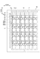
図1は、従来の有機ELパネルの一例となる有機ELパネル50の全体のレイアウトを回路構成とともに示した模式図である。有機ELパネル50は、画素ごとに表示駆動されるアクティブマトリックス型の表示装置である。各画素は、矩形形状を有する基板P上に樹脂などの隔壁によって区画され、それぞれ矩形形状の領域を有している。そして、基板Pのほぼ中央部分に互いに略直交する方向となるX方向およびY方向に規則正しく配列されて表示範囲を形成している。もとより、各画素は長円形状や円形状など矩形形状以外の形状を有する領域に区画されていてもよい。
FIG. 1 is a schematic diagram showing an entire layout of an
各画素には、有機EL素子が表示素子として、また、有機EL素子を表示(つまり発光)駆動するためのTFT(薄膜トランジスタ)54,55と保持容量56とが駆動素子として、それぞれ形成されている。なお、ここでは有機EL素子は、基板Pに対して表示素子の形成面側から光を射出するトップエミッション構造を有しているものとする。従って、駆動素子は表示素子と平面的に重なる位置であって、基板Pと表示素子との間に形成されている。もとより、有機EL素子は、トップエミッション構造でなく、基板Pに対して表示素子の形成面側と反対側から光を射出するボトムエミッション構造であっても差し支えない。
In each pixel, an organic EL element is formed as a display element, and TFTs (thin film transistors) 54 and 55 for driving (displaying light emission) the organic EL element and a
基板Pの外周部分には、走査駆動回路51とデータ駆動回路52、および給電端子53とが形成されている。走査駆動回路51からは走査線Gateが、データ駆動回路52からはデータ線Sigが、また、給電端子53からはこれに接続された電源供給線Comが、それぞれ各画素に形成された駆動素子に対して図1に示したように配線され、表示素子を発光駆動する。
On the outer peripheral portion of the substrate P, a
まず、走査線Gateは、TFT54のゲートに接続され、走査線Gateを介して供給される電流信号に応じて、TFT54をオン/オフ制御する。そしてTFT54がオンすると、TFT54のソースに接続されたデータ線Sigから供給される画像信号に応じて、電源供給線Comから供給される電源によって保持容量56に所定の電圧が保持される。すると、保持容量56に保持された電圧は、TFT55のゲートに印加され、TFT55をオン状態にする。TFT55のソースおよびドレインはそれぞれ電源供給線Comと画素電極としての陽極に接続され、保持容量56に保持された電圧に応じた、つまり画像信号に応じた電流が、電源供給線Comを介して陽極に印加される。
First, the scanning line Gate is connected to the gate of the
各画素に形成される表示素子は、陽極と対向電極としての陰極との間に電流を流すことによって発光する。つまり、陽極に印加された電流が、総ての画素の表面に渡って形成された陰極に流れることによって、画像信号に応じた明るさで発光するのである。従って、有機ELパネル50では、このように、駆動素子によるスイッチング動作を画像信号に応じて画素毎に制御することによって、種々の画像を表示することが行われている。
The display element formed in each pixel emits light by passing a current between the anode and the cathode as the counter electrode. That is, the current applied to the anode flows to the cathode formed over the surface of all the pixels, so that light is emitted with brightness according to the image signal. Therefore, in the
また、カラー画像を表示するために、各画素に形成される表示素子は、R(レッド)、G(グリーン)、B(ブルー)のうちいずれか1色を発光可能に形成され、画像や文字などの所定のカラー画像を表示するように構成される場合もある。なお、ここでは、説明を簡単にするために、図1に示すように、有機ELパネル50には、Y方向(図面縦方向)に4画素、X方向(図面横方向)に6画素の計24個の画素が配列された表示範囲が形成されているものとしたが、もとより、実際には、X,Yそれぞれの方向に数百画素といった多くの画素が配列されて表示範囲が形成されていることは言うまでもない。
In addition, in order to display a color image, a display element formed in each pixel is formed so as to be able to emit any one color of R (red), G (green), and B (blue). In some cases, a predetermined color image is displayed. Here, for simplicity of explanation, as shown in FIG. 1, the
さて、このような構成を有する従来の有機ELパネル50において、表示範囲に表示する文字や図柄や画像(これらを総称して「画像」と呼ぶ)が予め定められた画像、つまり固定画像を表示する場合がある。このような場合、表示範囲における総ての画素のうち、発光する画素を、固定画像の表示内容に応じて一意的に定めることができる。従って、固定画像を表示する場合は、画像信号に応じた駆動素子のスイッチング動作を画素毎に行うことを必ずしも必要とせず、固定画像に応じて、固定画像の表示を行う画素として定めた画素に陽極に電圧が印加されるようにすればよいことになる。
Now, in the conventional
そこで、本実施形態の有機ELパネルは、一例として2つの固定画像を、表示範囲全体に別々に表示するようにしたものであり、従って駆動素子のスイッチング動作が不要で、構造が簡単な有機ELパネルを提供するものである。また、これに加えて、表示される2つの固定画像のそれぞれについて、表示品質の低下を抑制するように工夫をしたものである。それでは、本実施形態の有機ELパネルについて、以下、図を参照して説明する。 Therefore, the organic EL panel according to the present embodiment displays two fixed images as an example separately over the entire display range, and therefore does not require a switching operation of the drive element and has a simple structure. A panel is provided. In addition to this, each of the two fixed images to be displayed is devised so as to suppress a decrease in display quality. The organic EL panel of this embodiment will be described below with reference to the drawings.
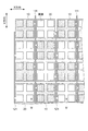
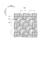
図2は、本実施形態の有機ELパネル100の全体のレイアウトを回路構成とともに示した模式図である。有機ELパネル100は、表示する固定画像に応じて各画素に形成された画素電極としての陽極を電気的に接続した表示装置である。各画素は、矩形形状を有する基板P上に樹脂などの隔壁によって区画され、それぞれ略正方形の矩形形状領域を有している。そして、基板Pのほぼ中央部分に、互いに交差する方向を有するX方向およびY方向に規則正しく配列されて表示範囲を形成している。
FIG. 2 is a schematic diagram showing the entire layout of the
本実施形態ではX方向とY方向とは略直交する方向であるものとする。もとより、これに限らず、直角以外の角度で交差しているものとしても差し支えない。また、本実施形態では、説明を簡単にするために、図2に示すように、有機ELパネル100には、Y方向(図面縦方向)に20画素、X方向(図面横方向)に16画素の計320個の画素が配列された表示範囲が形成されているものとする。もとより、実際には、X,Yそれぞれの方向に数百画素といった多くの画素が配列されて表示範囲が形成されていることは言うまでもない。また、各画素は正方形以外の矩形形状や、長円形状や円形状などの矩形形状以外の形状を有する領域に区画されていても差し支えない。
In the present embodiment, it is assumed that the X direction and the Y direction are substantially orthogonal to each other. Of course, the present invention is not limited to this, and it may be crossed at an angle other than a right angle. Further, in the present embodiment, for simplicity of explanation, as shown in FIG. 2, the
各画素には、有機EL素子が表示素子として形成されている。なお、ここでは有機EL素子は、発光時は白色光を発光するものとする。もとよりこれに限るものでないことは勿論であり、白色以外の一色を発光することとしてもよい。また、発光光を基板Pに対して表示素子の形成面側から射出するトップエミッション構造を有しているものとする。もとより、有機EL素子は、トップエミッション構造でなく、基板Pに対して表示素子の形成面側と反対側から光を射出するボトムエミッション構造であっても差し支えない。 In each pixel, an organic EL element is formed as a display element. Here, the organic EL element emits white light when emitting light. Of course, the present invention is not limited to this, and one color other than white may be emitted. Further, it is assumed that the substrate has a top emission structure that emits emitted light from the display element forming surface side with respect to the substrate P. Of course, the organic EL element may have a bottom emission structure in which light is emitted from the side opposite to the display element forming surface side with respect to the substrate P instead of the top emission structure.
また、本実施形態では、各画素には、X,Yそれぞれの方向に隣り合う2画素ずつの合計4画素を1つの纏まり(これを、以降「単位画素領域」と称す)として、互いに共通な1つの陽極が形成されている。そして、表示範囲に表示する2つの固定画像の一方(これを「画像A」とする)を表示するための単位画素領域には互いに共通な1つの陽極10(図中実線)が形成され、2つの固定画像の他方(これを「画像B」とする)を表示するための単位画素領域には互いに共通な1つの陽極20(図中破線)が形成されている。そして、陽極10と陽極20は、X,Yのそれぞれの方向において、陽極10同士、および陽極20同士が隣り合うことがないように交互に形成されている。
Further, in this embodiment, each pixel has a total of four pixels, each of two pixels adjacent in the X and Y directions, as one group (hereinafter referred to as “unit pixel region”), and is common to each other. One anode is formed. Then, one common anode 10 (solid line in the figure) is formed in the unit pixel area for displaying one of the two fixed images (this is referred to as “image A”) displayed in the display range. One common anode 20 (broken line in the figure) is formed in the unit pixel region for displaying the other of the two fixed images (hereinafter referred to as “image B”). The
基板Pの外周部分には、給電端子110と給電端子120とが形成されている。給電端子110には、電源供給線111が接続配線されている。また、給電端子120には、電源供給線121が接続配線されている。
A
電源供給線111は、表示範囲に画像Aを表示するとき、給電端子110に供給された所定の電圧を、形成された総ての陽極10に供給するように配線されている。同じく、電源供給線121は、表示範囲に画像Bを表示するとき、給電端子120に供給された所定の電圧を、形成された総ての陽極20に供給するように配線されている。そして、総ての画素の表面に渡って形成された対向電極としての陰極との間で電流が流れることによって、各画素に形成された有機EL素子が発光駆動され、画像Aあるいは画像Bを表示するように構成されている。
The
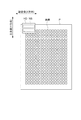
電源供給線111および電源供給線121と、陽極10および陽極20との具体的な配線の様子を、図3を用いて説明する。図3は、陽極10および陽極20と、電源供給線111および電源供給線121との電気的な接続の様子を示す模式図で、図2において円(一点鎖線)で囲んだ部分を拡大して示したものである。
A specific wiring state between the
図示するように、電源供給線111および電源供給線121は、X方向における陽極10または陽極20の端部、および陽極10と陽極20との隙間において、Y方向に延在してそれぞれ配線されている。また、電源供給線111と電源供給線121は、X方向において、陽極10と陽極20との隙間一つ置きに交互に形成されている。そして、電源供給線111は、その電源供給線111が延在するY方向に沿って存在する総ての陽極10と電気的に結線され、電源供給線121は、その電源供給線121が延在するY方向に沿って存在する総ての陽極20と電気的に結線されている。このように配線することによって、陽極10と陽極20との隙間に形成する配線を少なくすることができる。ちなみに、本実施形態では、電源供給線111もしくは電源供給線121のいずれかが配線できる隙間があればよいので、陽極の面積つまり画素の領域面積を大きくすることができる。この結果、画像Aあるいは画像Bについて明るさの減少を抑制することができる。
As shown in the figure, the
次に、本実施形態における有機ELパネル100に形成される有機EL素子について、図4を参照して詳しく説明する。図4は、本実施形態の有機ELパネル100における各画素に形成される機能層の構成を示す模式図である。図4(a)は、図3におけるM−M断面を示した模式断面図で、有機EL素子の形成が終了した状態を示した模式図である。また、図4(b)は、有機EL素子の発光層を機能液の噴射によって塗布して形成する様子を示した模式図である。なお、各寸法は、説明の都合上必要に応じて誇張しているため、実際の寸法とは必ずしも一致していないことは言うまでもない。
Next, the organic EL element formed in the
各画素は、図4(a)に示したように、エッチング等によって形成された絶縁有機材料(例えばアクリル樹脂やポリイミド樹脂)からなる隔壁によって区画された画素領域を有している。そして各画素の画素領域には、白色を発光可能な有機EL素子が形成されている。有機EL素子は、図示するように、陽極10あるいは陽極20と陰極との間に、正孔注入層と発光層とが形成されたものである。従って、各画素は、形成される発光層に依存して所定の明るさと発光色(本実施形態では白色)を発光する画素となる。
As shown in FIG. 4A, each pixel has a pixel region defined by a partition made of an insulating organic material (for example, acrylic resin or polyimide resin) formed by etching or the like. An organic EL element capable of emitting white light is formed in the pixel region of each pixel. As shown in the figure, the organic EL element has a hole injection layer and a light emitting layer formed between the
本実施形態では、正孔注入層は、PEDOT(ポリエチレンジオキシチオフェン)/PSS(ポリスチレンスルフォン酸)膜である。また、発光層は、白色を示す蛍光材料を溶質とした機能液を、各画素領域に所定量吐出し、以降真空乾燥および窒素雰囲気中での熱処理を行って、それぞれ所定の厚さの膜を形成したものである。 In the present embodiment, the hole injection layer is a PEDOT (polyethylenedioxythiophene) / PSS (polystyrene sulfonic acid) film. In addition, the light emitting layer discharges a predetermined amount of a functional liquid having a fluorescent material showing white as a solute to each pixel region, and then performs vacuum drying and heat treatment in a nitrogen atmosphere to form a film having a predetermined thickness. Formed.
隔壁の下には電源供給線111と電源供給線121が形成され、隔壁と陽極10,20との間に形成された無機絶縁膜によって、電源供給線111は陽極20に対して、電源供給線121は陽極10に対して、それぞれ絶縁されている。また、無機絶縁膜は、矩形形状の画素領域の外周に沿って所定幅が画素領域内に露出するように形成されている。これは、正孔注入層や発光層を形成する機能液との親液性を高め、正孔注入層や発光層が隔壁近傍まで形成されることによって、陽極10,20と陰極との間の短絡を防止するようにするためである。もとより、正孔注入層や発光層が隔壁近傍まできちんと形成できる場合は、無機絶縁膜は必ずしも形成する必要はない。無機絶縁膜を形成しない場合は、隔壁によって、電源供給線111と陽極20との間の絶縁、および電源供給線121と陽極10との間の絶縁を行うように構成すればよい。
A
また、本実施形態の表示素子は、トップエミッション方式の有機EL素子であることから、発光光が陰極側から射出するように、陽極10,20の基板Pと対向する面側には、Alなどによって反射層が形成されている。もとより、陽極10,20が反射層を兼ねる場合は、反射層を形成する必要はない。
Further, since the display element of this embodiment is a top emission type organic EL element, Al or the like is provided on the surface side of the
陽極10,20としては、ITO(酸化インジウムスズ)のように光透過性のある材料に限らず、酸化錫や金、銀、銅などの非光透過性の材料であっても使用可能である。また、陰極はITOなどの光透過性を有する材料で形成されている。もとより、金属材料であっても光が透過する程度に薄く形成されたものであれば陰極材料として使用してもよい。本実施形態では、陰極は電子注入層を兼ねており、例えば、LiF(フッ化リチウム)とAl(アルミニウム)をそれぞれ蒸着して形成したものである。
The
本実施形態では、上述したように、それぞれ対応する画素領域に有機発光材料を含む機能液を吐出して塗布するインクジェット方式によって発光層を形成するものである。具体的には、図4(b)に示したように、吐出ヘッドHDに設けられた不図示のノズルから、各画素に対応するそれぞれの画素領域に機能液を吐出することによって、各機能液を塗布する。その後、前述したように真空乾燥および窒素雰囲気中での熱処理を行うことによって各画素領域に発光層を形成するのである。ちなみに、図4(b)は、吐出ヘッドHDから発光層を形成する機能液を吐出する状態を示している。なお、正孔注入層も機能液を吐出して形成することとしても差し支えない。 In this embodiment, as described above, the light emitting layer is formed by an inkjet method in which a functional liquid containing an organic light emitting material is discharged and applied to each corresponding pixel region. Specifically, as shown in FIG. 4B, each functional liquid is ejected from a nozzle (not shown) provided in the ejection head HD to each pixel area corresponding to each pixel. Apply. Thereafter, as described above, a light emitting layer is formed in each pixel region by performing vacuum drying and heat treatment in a nitrogen atmosphere. Incidentally, FIG. 4B shows a state in which the functional liquid for forming the light emitting layer is ejected from the ejection head HD. The hole injection layer may also be formed by discharging a functional liquid.
ここで、本実施形態における吐出ヘッドHDに形成されたノズルについて、図5を用いて説明する。図5は、吐出ヘッドHDに穿設されたノズルの配列具合を示す模式図であり、図4(b)において図面下方向から見た状態を示したものである。 Here, the nozzles formed in the ejection head HD in the present embodiment will be described with reference to FIG. FIG. 5 is a schematic view showing the arrangement of the nozzles drilled in the ejection head HD, and shows a state seen from the lower side of the drawing in FIG.
本実施形態では、図示するように、吐出ヘッドHDは、各機能液体を吐出するノズル群NBを2つ備えている。ノズル群NBは、X方向(図面横方向)にノズルが略一直線に並んだノズル列を有し、その配列方向はX方向と一致している。もとより、ノズル列はX方向に対して傾いているなど、必ずしもX方向と一致しなくても差し支えない。 In the present embodiment, as illustrated, the ejection head HD includes two nozzle groups NB that eject each functional liquid. The nozzle group NB has a nozzle row in which nozzles are arranged in a substantially straight line in the X direction (the horizontal direction in the drawing), and the arrangement direction thereof coincides with the X direction. Of course, the nozzle row is not necessarily coincident with the X direction, for example, inclined with respect to the X direction.
穿設された各ノズルには、吐出ヘッドHD内において、前述したようにノズル毎に吐出機構がそれぞれ形成され、吐出ヘッドHD内の機能液に圧力を発生させて、所定量の機能液をノズルから吐出するように構成されている。もとより、吐出機構は、総てのノズルについて同様な構造を有している。 Each nozzle is provided with a discharge mechanism for each nozzle as described above in the discharge head HD, and a pressure is generated on the functional liquid in the discharge head HD so that a predetermined amount of the functional liquid is supplied to the nozzle. It is comprised so that it may discharge from. Of course, the discharge mechanism has the same structure for all nozzles.
吐出機構は、本実施形態では図5の吹出し部に示した構造を有し、圧電素子2を駆動体(アクチュエータ)とするものである。すなわち、圧電素子2は、その両端の電極COMとGNDとの間に所定の電圧波形が印加されると、電歪性によって収縮あるいは伸長変形して振動板3を図中矢印方向に撓ませて、流路途中に形成された加圧室4に存在する機能液を加圧する。この結果、加圧された機能液は、吐出ヘッドHDの底面部材8に穿設されたノズルから、液滴9として吐出されるのである。なお、吐出機構は、例えば、駆動体として加熱素子を用いた所謂サーマル方式などを採用することもできる。
In the present embodiment, the discharge mechanism has the structure shown in the blow-out portion of FIG. 5 and uses the
さて、このようにインクジェット方式を用いて機能液を吐出して有機EL素子を形成するとき、画像の表示範囲全体において、本実施形態では前述した各単位画素領域つまり陽極10,20に含まれる4つの画素毎に、画像Aまたは画像Bに応じて吐出すべき機能液を選択して吐出する。これを表示範囲における総ての単位画素領域について行うことによって、総ての画素に対して機能液を吐出するのである。
When forming an organic EL element by ejecting a functional liquid using the ink jet method in this way, in the present embodiment, the entire pixel display area includes the above-described unit pixel regions, that is, the
具体的には、図6に模式的に示した走査方法のように、Y方向(図面上下方向)を主走査方向とし、X方向(図面左右方向)を副走査方向として、基板Pと吐出ヘッドHDとを相対移動させる。このとき、吐出ヘッドHDに設けられた2つのノズル群NBから、各画素に応じた機能液を選択して吐出する。すなわち、吐出ヘッドHDにおける2つのノズル群NBから、有機発光材料を含む機能液と、絶縁性の有機化合物を材料として含む機能液とを、画像Aまたは画像Bに応じて吐出する。従って、各画素は、画像Aまたは画像Bに応じて、一意的に、発光材料を含む機能液によって発光層が形成された画素(つまり発光する画素)か、前記発光層に代えて、絶縁性の有機化合物を材料として含む機能液によって発光しない絶縁層が形成された画素(つまり発光しない画素)か、のいずれかになる。ここで絶縁性の有機化合物としては、遮光性を有するものを用いても良い。このようにすれば、発光しない画素から光が漏れるのを防ぐことができる。 Specifically, as in the scanning method schematically shown in FIG. 6, the substrate P and the ejection head are set with the Y direction (up and down direction in the drawing) as the main scanning direction and the X direction (left and right direction in the drawing) as the sub scanning direction. Move relative to HD. At this time, the functional liquid corresponding to each pixel is selected and discharged from the two nozzle groups NB provided in the discharge head HD. That is, a functional liquid containing an organic light emitting material and a functional liquid containing an insulating organic compound as a material are discharged from the two nozzle groups NB in the discharge head HD according to the image A or the image B. Accordingly, each pixel is uniquely a pixel in which a light emitting layer is formed with a functional liquid containing a light emitting material (that is, a light emitting pixel) according to the image A or the image B, or an insulating property instead of the light emitting layer. Or a pixel having an insulating layer that does not emit light (that is, a pixel that does not emit light). Here, as the insulating organic compound, a light-blocking compound may be used. In this way, it is possible to prevent light from leaking from pixels that do not emit light.
この一例を、図7を用いて説明する。図7(a)は、画像Aとしてローマ字の「E」を表示する場合を示し、図7(b)は、画像Bとしてローマ字の「P」を表示する場合を示した説明図である。 An example of this will be described with reference to FIG. FIG. 7A shows a case where the Roman letter “E” is displayed as the image A, and FIG. 7B is an explanatory view showing a case where the Roman letter “P” is displayed as the image B.
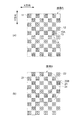
まず、図7(a)に示したように、画像Aでは、表示するローマ字「E」の大きさと形が二点鎖線に示した画像であった場合、網掛けで示した発光する画素(例えば画素11)と、白抜きで示した発光しない画素(例えば画素12)のいずれかに、それぞれ一意的に区分される。従って、画像Aの一部の画像をそれぞれ分担して表示する単位画素領域における4つの画素は、総ての画素が発光する、あるいは総ての画素が発光しない、あるいは発光する画素と発光しない画素が共存する、のいずれかになる。一例として図中破線で示した単位画素領域である陽極10Aにおいては、発光する画素14と発光しない画素13の両方が存在する。
First, as shown in FIG. 7A, in the image A, when the size and shape of the Roman letter “E” to be displayed is an image indicated by a two-dot chain line, the light emitting pixels (for example, shaded) (for example, The pixel 11) and the non-light-emitting pixel (for example, the pixel 12) shown in white are each uniquely divided. Accordingly, the four pixels in the unit pixel area for displaying a part of the image A in a shared manner are all pixels that emit light, or that all pixels do not emit light, or pixels that do not emit light and pixels that do not emit light. Will coexist. As an example, in the
同様に、図7(b)に示したように、画像Bでは、表示するローマ字「P」の大きさと形が二点鎖線に示した画像であった場合、網掛けで示した発光する画素(例えば画素21)と、白抜きで示した発光しない画素(例えば画素22)のいずれかに、それぞれ一意的に区分される。従って、画像Bの一部の画像をそれぞれ分担して表示する単位画素領域における4つの画素は、総ての画素が発光する、あるいは総ての画素が発光しない、あるいは発光する画素と発光しない画素が共存する、のいずれかになる。一例として図中破線で示した単位画素領域である陽極20Bにおいては、発光する画素24と発光しない画素23の両方が存在する。
Similarly, as shown in FIG. 7B, in the image B, when the size and shape of the Roman letter “P” to be displayed is an image indicated by a two-dot chain line, the light emitting pixel ( For example, each pixel is uniquely divided into a pixel 21) and a non-light-emitting pixel (for example, pixel 22) shown in white. Accordingly, the four pixels in the unit pixel area for displaying a part of the image B in a shared manner are all pixels that emit light, or that all pixels do not emit light, or pixels that do not emit light and pixels that do not emit light. Will coexist. As an example, in the
従って、上述の説明から容易に理解できるように、画像A,画像Bの表示をそれぞれ分担する各単位画素領域において、画像A,画像Bとして表示する画像の内容に応じて、発光する画素と発光しない画素が異なることになる。つまり、表示する画像に応じて、1つの画素が発光する画素になったり発光しない画素になったりすることになるのである。そのために、前述するように、画素毎に発光層として吐出する機能液を、有機発光材料を含む機能液とするか、絶縁性の有機化合物を材料として含む機能液とするかによって、1つの画素を、発光する画素としたり、発光しない画素としたりすることができるのである。 Therefore, as can be easily understood from the above description, in each unit pixel area that shares the display of the images A and B, the light emitting pixels and the light emission according to the contents of the images displayed as the images A and B. The pixels that do not differ. That is, depending on the image to be displayed, one pixel may become a pixel that emits light or a pixel that does not emit light. Therefore, as described above, one pixel is selected depending on whether the functional liquid discharged as a light emitting layer for each pixel is a functional liquid containing an organic light emitting material or a functional liquid containing an insulating organic compound as a material. The pixel can be a pixel that emits light or a pixel that does not emit light.
なお、本実施形態では、画像A,画像Bについて、上述したように少なくとも発光層を機能液の吐出によって形成する。そして、Y方向を主走査方向として機能液を吐出するため、Y方向に並んだ画素は同じノズルから機能液が吐出される。このため、画素がY方向において隙間無く並んでいる場合は、ノズル間で少なからず生ずる機能液の吐出量の差異に起因する縦縞の輝度ムラが視認される虞があるが、本実施形態では、Y方向において、画素が1つの単位画素領域飛び、つまり2画素置きに2画素が存在するという不連続配列になるため、縦縞の輝度ムラが視認されにくいという利点を有する。 In the present embodiment, for the images A and B, at least the light emitting layer is formed by discharging the functional liquid as described above. Since the functional liquid is discharged with the Y direction as the main scanning direction, the functional liquid is discharged from the same nozzle to the pixels arranged in the Y direction. For this reason, when the pixels are arranged without gaps in the Y direction, there is a possibility that uneven luminance of vertical stripes due to a difference in the discharge amount of the functional liquid generated between the nozzles may be visually recognized. In the Y direction, the pixels jump in one unit pixel area, that is, there is a discontinuous arrangement in which two pixels exist every two pixels. Therefore, there is an advantage that uneven luminance of vertical stripes is difficult to be visually recognized.
上述したように、本実施形態の有機ELパネルによれば、陽極と陰極との間に電圧を印加することによって、画像Aもしくは画像Bのいずれかに属するように電気的に接続された総ての単位画素領域における画素に同時に電圧を印加することができる。この結果、発光すべき画素が同時に発光することによって、画像Aもしくは画像Bを表示範囲に表示することができる。従って、画素毎に駆動素子によるスイッチング動作を制御することなく、表示範囲のほぼ全体に1つの画像を容易に表示させることができるのである。 As described above, according to the organic EL panel of the present embodiment, all the electrodes electrically connected to belong to either the image A or the image B by applying a voltage between the anode and the cathode. A voltage can be simultaneously applied to the pixels in the unit pixel region. As a result, the image A or the image B can be displayed in the display range by simultaneously emitting light to be emitted. Therefore, one image can be easily displayed on almost the entire display range without controlling the switching operation by the driving element for each pixel.
また、本実施形態では、図7に示したように、4つの画素からなる単位画素領域が、X,Y方向においてそれぞれ隣り合うことなく、ほぼ表示範囲全体に配置される。従って、単位画素領域が表示範囲全体に分散することになり、複数の画像を、それぞれ表示範囲全体に分散した単位画素領域によって表示することができるので、表示されるそれぞれの画像A,画像Bは、その表示面積がおおよそ同じ画像になる。また、単位画素領域の分散によって、表示面積に対する単位画素領域の分布密度が、表示される画像A,画像Bのそれぞれにおいて凡そ同じになる。この結果、表示されるそれぞれの画像A,画像Bは表示品質の低下が抑制された画像となる。 Further, in the present embodiment, as shown in FIG. 7, the unit pixel area composed of four pixels is arranged almost in the entire display range without being adjacent to each other in the X and Y directions. Accordingly, the unit pixel area is distributed over the entire display range, and a plurality of images can be displayed by the unit pixel area distributed over the entire display range, so that each of the displayed images A and B is The display area is approximately the same image. Further, due to the dispersion of the unit pixel regions, the distribution density of the unit pixel regions with respect to the display area is approximately the same in each of the displayed image A and image B. As a result, each of the displayed images A and B is an image in which deterioration of display quality is suppressed.
なお、画像Aおよび画像Bの表示に際して、それぞれの給電端子110および給電端子120からそれぞれの画像に属する総ての単位画素領域に流れる電流の総和は、表示される画像A,画像Bのそれぞれにおいて単位画素領域の分布密度が凡そ同じであることから、ほぼ同じになる確率が高くなる。従って、それぞれの給電端子110および給電端子120に対して、供給できる電流容量が同じ電源回路を用いて電圧を印加することができるので、複数の電源回路を設計する必要がなく、電源回路に対する設計負荷が軽減される効果も奏する。
It should be noted that when images A and B are displayed, the sum of the currents flowing from the respective
以上、本発明について、実施形態を用いて説明したが、本発明はこうした実施形態に何ら限定されるものではなく、本発明の趣旨を逸脱しない範囲内において様々な形態で実施し得ることは勿論である。以下変形例を挙げて説明する。 As mentioned above, although this invention was demonstrated using embodiment, this invention is not limited to such embodiment at all, Of course, in the range which does not deviate from the meaning of this invention, it can implement with various forms. It is. Hereinafter, a modification will be described.
(第1変形例)
上記実施形態では、表示範囲において、2つの画像(画像A、画像B)を表示することとして説明したが、これに限らずさらに多くの数の画像を表示することとしてもよい。一例として、3つの画像(画像A、画像B、画像C)を表示する場合を図8を参照して、4つの画像(画像A、画像B、画像C、画像D)を表示する場合を図9を参照して、それぞれ説明する。
(First modification)
In the embodiment described above, two images (image A and image B) are displayed in the display range. However, the present invention is not limited to this, and a larger number of images may be displayed. As an example, a case where three images (image A, image B, image C) are displayed is illustrated with reference to FIG. 8, and a case where four images (image A, image B, image C, image D) are displayed is illustrated. Each will be described with reference to FIG.
(3つの画像表示)
図8は、基板P上における配線状態の一部を示した模式図である。本変形例においても、上記実施形態と同様、各画素の陽極は4つの画素(不図示)を1つの単位画素領域とするように陽極10、陽極20、陽極30に分割形成されている。そして、X方向には陽極10、陽極20、陽極30の順で繰り返して存在し、Y方向には陽極10、陽極30、陽極20の順で繰返し存在するように配置されている。陽極10,20,30はそれぞれ斜め方向において相互に電気的に接続されている。
(3 image displays)
FIG. 8 is a schematic diagram showing a part of the wiring state on the substrate P. As shown in FIG. Also in this modification, as in the above embodiment, the anode of each pixel is divided into the
ここでは、陽極10が画像Aに、陽極20が画像Bに、陽極30が画像Cに、それぞれ属する画像を表示するように構成されている。すなわち、給電端子110には画像Aを表示するための電圧が印加され、給電端子110からX,Y両方向に延在する電源供給線111によって、総ての陽極10が給電端子110と電気的に接続される。給電端子120には画像Bを表示するための電圧が印加され、給電端子120からX,Y両方向に延在する電源供給線121によって、総ての陽極20が給電端子120と電気的に接続される。また、給電端子130には画像Cを表示するための電圧が印加され、給電端子130からX,Y両方向に延在する電源供給線131によって、総ての陽極30が給電端子130と電気的に接続される。
Here, the
このような陽極の分割形成によって、表示範囲において3つの画像を表示する際、図示するように、1つの画像を表示する単位画素領域がX方向およびY方向において隣り合うことがなく一定の間隔で表示範囲全体に分散することになる。従って、3つの画像を、それぞれ表示範囲全体に分散した単位画素領域によって表示することができる。 By displaying the three images in the display range by dividing the anode in this way, as shown in the figure, the unit pixel regions for displaying one image are not adjacent to each other in the X direction and the Y direction at regular intervals. It will be distributed over the entire display range. Accordingly, the three images can be displayed by unit pixel areas that are dispersed over the entire display range.
この結果、表示されるそれぞれの画像A,B,Cは、それぞれの単位画素領域が存在する領域範囲となる表示面積がおおよそ同じ画像になる。また、単位画素領域が一定の間隔で分散することによって、表示面積に対する単位画素領域の分布密度が、表示される画像A,B,Cのそれぞれにおいて凡そ同じになる。この結果、表示されるそれぞれの画像A,B,Cの表示品質を凡そ同じにすることができる。 As a result, the displayed images A, B, and C are images having approximately the same display area as a region range in which each unit pixel region exists. In addition, since the unit pixel regions are dispersed at regular intervals, the distribution density of the unit pixel regions with respect to the display area is approximately the same in each of the displayed images A, B, and C. As a result, the display quality of the displayed images A, B, and C can be made substantially the same.
(4つの画像表示)
図9は、図8同様、基板P上における配線状態の一部を示した模式図である。ここでも、上記実施形態と同様、各画素の陽極は、それぞれ4つの画素(不図示)を1つの単位画素領域とするように陽極10、陽極20、陽極30、陽極40に分割形成されている。そして、X方向には陽極10、陽極20の順、もしくは陽極30、陽極40の順で繰り返して存在し、Y方向には陽極10、陽極30、もしくは陽極20、陽極40の順で繰返し存在するように配置されている。
(4 image display)
FIG. 9 is a schematic diagram showing a part of the wiring state on the substrate P, as in FIG. Here, as in the above embodiment, the anode of each pixel is divided into the
ここでは、陽極10が画像Aに、陽極20が画像Bに、陽極30が画像Cに、陽極40が画像Dに、それぞれ属する画像を表示するように構成されている。すなわち、給電端子110には画像Aを表示するための電圧が印加され、給電端子110からX方向に延在する電源供給線111と、この電源供給線111に接続されY方向に延在する配線112とによって、総ての陽極10が給電端子110と電気的に接続される。同様に、給電端子120には画像Bを表示するための電圧が印加され、給電端子120からX方向に延在する電源供給線121と、この電源供給線121に接続されY方向に延在する配線122とによって、総ての陽極20が給電端子120と電気的に接続される。給電端子130には画像Cを表示するための電圧が印加され、給電端子130からX方向に延在する電源供給線131と、この電源供給線131に接続されY方向に延在する配線132とによって、総ての陽極30が給電端子130と電気的に接続される。給電端子140には画像Dを表示するための電圧が印加され、給電端子140からX方向に延在する電源供給線141と、この電源供給線141に接続されY方向に延在する配線142とによって、総ての陽極40が給電端子140と電気的に接続される。
Here, the
このような陽極の分割形成によって、表示範囲において4つの画像を表示する際、図示するように、1つの画像を表示する単位画素領域がX方向およびY方向において隣り合うことがなく一定の間隔で表示範囲全体に分散することになる。従って、4つの画像を、それぞれ表示範囲全体に分散した単位画素領域によって表示することができる。 When four images are displayed in the display range by dividing the anode in this way, unit pixel regions for displaying one image are not adjacent to each other in the X direction and the Y direction, as shown in the drawing, at a constant interval. It will be distributed over the entire display range. Therefore, the four images can be displayed by unit pixel areas distributed over the entire display range.
この結果、表示されるそれぞれの画像A,B,C,Dは、それぞれの単位画素領域が存在する領域範囲となる表示面積がおおよそ同じ画像になる。また、単位画素領域が一定の間隔で分散することによって、表示面積に対する単位画素領域の分布密度が、表示される画像A,B,C,Dのそれぞれにおいて凡そ同じになる。この結果、表示されるそれぞれの画像A,B,C,Dの表示品質を凡そ同じにすることができる。 As a result, the displayed images A, B, C, and D are images having substantially the same display area as a region range in which each unit pixel region exists. In addition, since the unit pixel regions are dispersed at regular intervals, the distribution density of the unit pixel regions with respect to the display area is approximately the same in each of the displayed images A, B, C, and D. As a result, the display quality of the displayed images A, B, C, and D can be made substantially the same.
なお、陽極10,20,30,40の配置は図9に示した配置に限るものでないことは勿論である。例えば、X,Y両方向ともに、陽極10、陽極20、陽極30、陽極40の順で繰返し存在するように配置することとしてもよい。要は、X方向およびY方向において、電気的に接続された陽極が連続しない順序の配置であれば、いずれの配置も採用することが可能である。
Of course, the arrangement of the
(第2変形例)
上記実施形態では、表示範囲に表示される複数の画像について、それぞれの画像に属する単位画素領域の分布密度が、表示範囲において凡そ同じになるようにしたが、これに限らず、表示範囲に表示される画像が3つ以上の場合は、それぞれの画像に属する単位画素領域の分布密度が異なるようにしてもよい。こうすれば、表示範囲に表示する複数の画像について、例えば、それぞれの画像の表示内容を視認するために必要となる単位画素領域の分布密度に応じて、それぞれの画像に属する単位画素領域を配置することができる。
(Second modification)
In the above embodiment, the distribution density of the unit pixel areas belonging to each image is set to be substantially the same in the display range for a plurality of images displayed in the display range. When three or more images are to be displayed, the distribution density of the unit pixel regions belonging to each image may be different. In this way, for a plurality of images displayed in the display range, for example, unit pixel areas belonging to the respective images are arranged according to the distribution density of the unit pixel areas necessary for visually recognizing the display contents of each image. can do.
本変形例の一例を、図10を用いて説明する。図10は、基板P上における配線状態の一部を示した模式図であり、図8と同様、表示範囲に3つの画像を表示する場合を示したものである。本変形例においても、上記実施形態と同様、各画素の陽極は4つの画素(不図示)を1つの単位画素領域とするように陽極10、陽極20、陽極30に分割形成されている。そして、本変形例では、各陽極10〜30は、X,Y両方向ともに、陽極10、陽極20、陽極30、陽極20の順で繰り返して存在するように配置されている。また各陽極10,20,30はそれぞれ斜め方向において相互に電気的に接続されている。
An example of this modification will be described with reference to FIG. FIG. 10 is a schematic diagram showing a part of the wiring state on the substrate P, and shows the case where three images are displayed in the display range, as in FIG. Also in this modification, as in the above embodiment, the anode of each pixel is divided into the
本変形例においても、陽極10が画像Aに、陽極20が画像Bに、陽極30が画像Cに、それぞれ属する画像を表示するように構成されている。すなわち、給電端子110には画像Aを表示するための電圧が印加され、給電端子110からX,Y両方向に延在する電源供給線111によって、総ての陽極10が給電端子110と電気的に接続される。同様に、給電端子120には画像Bを表示するための電圧が印加され、給電端子120からX,Y両方向に延在する電源供給線121によって、総ての陽極20が給電端子120と電気的に接続される。また、給電端子130には画像Cを表示するための電圧が印加され、給電端子130からX,Y両方向に延在する電源供給線131によって、総ての陽極30が給電端子130と電気的に接続される。
Also in this modification, the
このような陽極の分割形成によって、表示範囲において3つの画像を表示する際、図中網掛けで示したように、画像Bに属する単位画素領域、すなわち陽極20の表示範囲全体に対する分布密度が、画像Aあるいは画像Cに属する単位画素領域の分布密度よりも高くなる。従って、表示範囲に表示する画像A,B,Cのうち、例えば画像Bについては他の画像よりも高解像度の表示が要求される画像であった場合、画像Bに属する単位画素領域の分布密度を高くすることによって、表示される画像A,B,Cのそれぞれの画像間において、表示品質の差異を抑制することが可能となる。
When three images are displayed in the display range by dividing the anode as described above, the distribution density of the unit pixel region belonging to the image B, that is, the entire display range of the
(第3変形例)
上記実施形態では、説明を容易にするため、各画素に形成される発光層の発光色は白色であることとして説明したが、もとよりこれに限るものでないことは勿論である。例えば、表示範囲にカラー画像を表示するために、発光する各画素に形成される有機EL素子は、R(レッド)、G(グリーン)、B(ブルー)のうちいずれか1色を発光可能に形成されていることとしてもよい。
(Third Modification)
In the above embodiment, the light emission color of the light emitting layer formed in each pixel has been described as white for the sake of easy explanation, but it is needless to say that the present invention is not limited to this. For example, in order to display a color image in the display range, the organic EL element formed in each pixel that emits light can emit any one of R (red), G (green), and B (blue). It may be formed.
本変形例の一例を図11を用いて説明する。図11は、表示範囲に2つの画像を表示する場合を示した模式図である。本変形例では、X,Y両方向に3画素ずつ、合計9画素を1つの単位画領域となるように陽極が分割形成されている。そして、図中実線で示した陽極10によって、2つの画像のうちの一方の画像Aが表示され、図中破線で示した陽極20によって、2つの画像のうちの他方の画像Bが表示されるように分割形成された各陽極10,20は、給電端子と接続配線(不図示)されている。
An example of this modification will be described with reference to FIG. FIG. 11 is a schematic diagram showing a case where two images are displayed in the display range. In this modification, the anodes are divided and formed so that a total of 9 pixels constitute one unit image area, 3 pixels in both the X and Y directions. Then, one image A of the two images is displayed by the
さて、いま画像Aが、図11に示したように「R、G、黒、B」の各色が繰返し存在する図中右肩上がりの斜めストライプ模様であった場合、各陽極10における9つの画素は、ストライプ模様に応じて、R(レッド)、G(グリーン)、B(ブルー)、のうちいずれか1色を発光可能な画素か、もしくは発光しない画素に形成される。例えば、陽極10aにおける9つの画素は、図示するように、R色を発光する3つの画素、G色を発光する5つの画素、発光しない1つの画素(網掛けした画素)、にそれぞれ形成される。また陽極10bにおける9つの画素は、図示するように、B色を発光する3つの画素、R色を発光する5つの画素、G色を発光する1つの画素、にそれぞれ形成される。
Now, when the image A is an oblique stripe pattern that rises to the right in the figure in which each color of “R, G, black, and B” repeatedly exists as shown in FIG. 11, nine pixels in each
なお、本変形例において、R光、G光、B光を発光する有機EL素子の形成をインクジェット方式を用いて行う場合は、前述した吐出ヘッドHDにおいて、R,G,B各色の有機発光材料を含む機能液を吐出するノズル群NBを備えればよい。 In this modification, in the case where the organic EL element that emits R light, G light, and B light is formed using an ink jet method, the organic light emitting material of each color of R, G, and B is used in the above-described ejection head HD. The nozzle group NB that discharges the functional liquid containing the liquid may be provided.
本変形例によれば、このように表示範囲に表示するカラー画像に応じて、各単位画素領域における画素の発光色を定めることによって、複数のカラー画像を表示することができる。また、発光層の発光色を決定する有機発光材料を含む機能液、もしくは絶縁性を有する有機化合物を含む機能液のいずれかを、インクジェット方式によって各画素に吐出するようにすれば、各画素に形成する発光層を、表示する画像に応じて任意に変更することが可能となる。 According to this modification, a plurality of color images can be displayed by determining the emission color of the pixels in each unit pixel region in accordance with the color image displayed in the display range. In addition, if any one of a functional liquid containing an organic light-emitting material that determines an emission color of a light-emitting layer or a functional liquid containing an insulating organic compound is discharged to each pixel by an inkjet method, The light emitting layer to be formed can be arbitrarily changed according to the image to be displayed.
(第4変形例)
また、上記第3変形例のさらに変形例として、表示範囲にカラー画像を表示する場合、1つの単位画素領域において、R,G,Bの各色を発光する画素数が、それぞれ同じになるように陽極が分割形成されることが好ましい。こうすれば、1つの単位画素領域において、R,G,B各色の発光輝度を調節することによって、1つの単位画素領域は、カラー画像の絵素として機能することになる。この結果、1つの単位画素領域毎に、R,G,B各色の発光輝度を調節すれば、総ての単位画素領域を用いて、表示範囲にカラー画像を表示することができる。
(Fourth modification)
As a further modification of the third modification, when a color image is displayed in the display range, the number of pixels that emit light of R, G, and B is the same in one unit pixel area. It is preferable that the anode is divided and formed. By doing so, one unit pixel area functions as a picture element of a color image by adjusting the emission luminance of each color of R, G, and B in one unit pixel area. As a result, if the emission brightness of each color of R, G, and B is adjusted for each unit pixel area, a color image can be displayed in the display range using all the unit pixel areas.
本変形例の一例を図12を用いて説明する。図12は、表示範囲に3つの画像を表示する場合を示した模式図である。本変形例では、1つの画素に対してX,Y両方向にそれぞれ1画素隣接した合計3画素を1つの単位画素領域となるように陽極が分割形成されている。そして、図中濃い網掛け部分で示した陽極10同士が、また図中薄い網掛け部分で示した陽極20同士が、また、図中白抜き部分で示した陽極30同士が、それぞれ1つの画像を表示するように、それぞれ1つの給電端子と接続配線(不図示)されている。この結果、1つの単位画素領域は、R,G,Bの各色を発光する画素が1つずつ含まれる所謂絵素として機能するのである。従って、このように陽極を分割することによって、長手方向を形成することなく画素が纏まった絵素とすることができることから、表示範囲に表示されるそれぞれの画像について表示品質の低下を抑制することができる可能性がある。もとより、X方向に隣り合う3画素、もしくはY方向に隣り合う3画素を、1つの単位画素領域としても差し支えない。
An example of this modification will be described with reference to FIG. FIG. 12 is a schematic diagram showing a case where three images are displayed in the display range. In this modification, the anodes are divided and formed so that a total of three pixels adjacent to one pixel in both the X and Y directions constitute one unit pixel region. The
そして、本変形例では、各画素に、R,G,B色のいずれかを発光する有機発光材料を含む機能液を吐出して発光層を形成する。このとき、インクジェット方式によって吐出する機能液の吐出量を、表示する画像に応じてR,G,B間で変更する。こうすることで、形成される発光層の厚さを変更することができるので、R,G,Bのそれぞれの発光色の輝度を、単位画素領域毎に変更することが可能となる。従って、単位画素領域つまり絵素毎にR,G,B各色の混合色を調節することができることから、カラー画像を適切に表示範囲に表示することができる。なお、本変形例では、単位画素領域全体を発光しない画素つまり黒色とする場合は、3つの画素総ての発光層を、絶縁性を有する有機化合物によって形成するようにすればよい。 In this modification, a functional liquid containing an organic light emitting material that emits one of R, G, and B colors is discharged to each pixel to form a light emitting layer. At this time, the discharge amount of the functional liquid discharged by the ink jet method is changed between R, G, and B according to the displayed image. By doing so, the thickness of the light emitting layer to be formed can be changed, so that the luminance of each of the R, G, and B emission colors can be changed for each unit pixel region. Therefore, since the mixed color of R, G, and B colors can be adjusted for each unit pixel area, that is, for each picture element, a color image can be appropriately displayed in the display range. In this modification, in the case where the entire unit pixel region is a pixel that does not emit light, that is, black, the light emitting layer of all three pixels may be formed of an organic compound having an insulating property.
なお、本変形例において、表示範囲の端部においては、単位画素領域を形成できない端数の画素が存在することになる。このような場合は、例えば図12における陽極30aのように、表示範囲の周辺に画素が存在するものとして陽極を分割形成して単位画素領域を形成すればよい。もとより、上記実施形態や上記変形例において、表示範囲の端部において単位画素領域を形成できない端数の画素が存在する場合は、本変形例と同様にすればよいことは言うまでもない。
In this modification, there are fractional pixels that cannot form a unit pixel region at the end of the display range. In such a case, the unit pixel region may be formed by dividing the anode so that pixels exist around the display range, such as the
(その他の変形例)
上記実施形態および上記変形例では、1つの単位画素領域は3つの画素、4つの画素、あるいは9つの画素によって形成されることとして説明したが、これに限るものでなく、1つの画素を含め任意の画素数によって形成されることとしても差し支えない。またX,Yそれぞれの方向に隣り合う画素の数も、特にこれに限るものでないことは勿論である。また、単位画素領域の形状も必ずしも同一でなくてもよい。さらに、1つの単位画素領域に含まれる画素数が、単位画素領域間で必ずしも同じでなくてもよい。
(Other variations)
In the embodiment and the modification described above, one unit pixel region has been described as being formed by three pixels, four pixels, or nine pixels. However, the present invention is not limited to this, and any unit pixel area is arbitrarily included. It may be formed by the number of pixels. Of course, the number of pixels adjacent in the X and Y directions is not limited to this. Further, the shape of the unit pixel area is not necessarily the same. Furthermore, the number of pixels included in one unit pixel area may not necessarily be the same between the unit pixel areas.
また、上記実施形態では、エレクトロルミネッセンス素子として有機EL素子を形成することとし、機能液の吐出によって塗布して形成する機能層が、発光層(および正孔注入層)であることとして説明したが、必ずしもこれに限るものでないことは勿論である。例えば、陰極とは別に電子注入層を形成する場合は、この電子注入層を液滴の噴射によって形成する機能層としてもよい。あるいは発光層が正孔注入層を兼用する場合は、発光層のみが機能液の吐出によって塗布形成される機能層であることとしてもよい。 In the above embodiment, the organic EL element is formed as the electroluminescence element, and the functional layer formed by applying and discharging the functional liquid is the light emitting layer (and the hole injection layer). Of course, it is not necessarily limited to this. For example, when an electron injection layer is formed separately from the cathode, the electron injection layer may be a functional layer formed by droplet ejection. Alternatively, when the light emitting layer also serves as the hole injection layer, only the light emitting layer may be a functional layer that is formed by application of functional liquid.
また、上記実施形態では、表示素子として有機EL素子を形成することとしたが、これに限らず、無機EL素子であっても差し支えない。また、エレクトロルミネッセンス素子に限らず、表示素子として機能するものであれば、必ずしもエレクトロルミネッセンス素子に限るものでないことは勿論である。例えば、画素領域に発光ダイオードを形成する場合としてもよい。勿論この場合は、形成される機能層は上記実施形態とは異なることは言うまでもない。 In the above embodiment, the organic EL element is formed as the display element. However, the present invention is not limited to this, and an inorganic EL element may be used. Of course, the element is not limited to the electroluminescence element as long as it functions as a display element without being limited to the electroluminescence element. For example, a light emitting diode may be formed in the pixel region. Of course, in this case, it goes without saying that the functional layer to be formed is different from the above embodiment.
2…圧電素子、4…加圧室、8…底面部材、9…液滴、10,10a,10A…陽極、10b…陽極、11〜14…画素、20,20B…陽極、21〜24…画素、30…陽極、40…陽極、50…有機ELパネル、51…走査駆動回路、52…データ駆動回路、53…給電端子、54,55…TFT、56…保持容量、100…有機ELパネル、110…給電端子、111…電源供給線、112…配線、120…給電端子、121…電源供給線、122…配線、130…給電端子、131…電源供給線、132…配線、140…給電端子、141…電源供給線、142…配線。
DESCRIPTION OF
Claims (9)
前記第1の方向及び当該第2の方向に沿って配列された複数の第2画素電極と、
前記複数の第1画素電極及び前記複数の第2画素電極に対向して形成された対向電極と、
前記複数の第1画素電極を電気的に接続する第1電源供給線と、
前記複数の第2画素電極を電気的に接続する第2電源供給線と、
を有し、
前記複数の第1画素電極及び前記複数の第2画素電極の各々の画素電極に対応して1つ又は複数の画素が形成されており、
前記複数の第1画素電極のうちの1つの画素電極である第1電極と前記対向電極との間及び前記複数の第2画素電極のうちの1つの画素電極である第2電極と前記対向電極との間には、有機発光材料によって形成された発光層、または、有機化合物によって形成された絶縁層が配置されており、
第1の画像を表示する際には、前記第1電源供給線を介して前記複数の第1画素電極に電源を供給し、第2の画像を表示する際には、前記第2電源供給線を介して前記複数の第2画素電極に電源を供給することを特徴とする表示装置。 A plurality of first pixel electrodes arranged along a first direction and a second direction intersecting the first direction;
A plurality of second pixel electrodes arranged along the first direction and the second direction;
A counter electrode formed to face the plurality of first pixel electrodes and the plurality of second pixel electrodes;
A first power supply line that electrically connects the plurality of first pixel electrodes;
A second power supply line for electrically connecting the plurality of second pixel electrodes;
Have
One or a plurality of pixels are formed corresponding to each pixel electrode of the plurality of first pixel electrodes and the plurality of second pixel electrodes,
Between the first electrode which is one pixel electrode of the plurality of first pixel electrodes and the counter electrode, and the second electrode which is one pixel electrode of the plurality of second pixel electrodes and the counter electrode Between the light emitting layer formed of an organic light emitting material or an insulating layer formed of an organic compound,
When displaying the first image, power is supplied to the plurality of first pixel electrodes via the first power supply line, and when displaying the second image, the second power supply line. A power supply is supplied to the plurality of second pixel electrodes through the display.
前記表示範囲は、1画素若しくは前記第1の方向および前記第2の方向に隣り合う2画素以上の画素の纏まりを単位画素領域として区分され、
前記単位画素領域のそれぞれは、前記複数の画像のうちの1つの画像に属する一部の画像を表示するとともに、前記第1の方向および前記第2の方向において隣り合う前記単位画素領域間では、それぞれの前記単位画素領域が表示する一部の画像が属する前記1つの画像が、互いに異なるように表示することを特徴とする表示装置。 A display range of an image in which a plurality of pixels are arranged in a matrix along a first direction and a second direction intersecting the first direction is displayed, and the plurality of images are displayed in the display range of the image. A display device,
The display range is divided into one pixel or a group of two or more pixels adjacent in the first direction and the second direction as a unit pixel region,
Each of the unit pixel regions displays a partial image belonging to one image of the plurality of images, and between the unit pixel regions adjacent in the first direction and the second direction, The display device, wherein the one image to which a part of images displayed by each unit pixel region belongs is displayed differently.
前記単位画素領域は、前記表示範囲の周辺部を除いて、当該単位画素領域に含まれる画素の配列状態が、総ての前記単位画素領域について同一であることを特徴とする表示装置。 The display device according to claim 3,
The display device according to claim 1, wherein the unit pixel region has the same arrangement state of pixels included in the unit pixel region except for a peripheral portion of the display range.
前記複数の画素は、第1の電極と、第2の電極と、当該第1の電極と当該第2の電極とによって挟持された発光層を含む有機層を有し、前記第1の電極と前記第2の電極との間に電流が流れることによって前記発光層が発光する画素であって、
前記第1の電極は、前記1つの画像に属する総ての前記単位画素領域に存在する画素間で電気的に接続され、前記第2の電極は、前記表示範囲に形成された総ての画素間で電気的に接続されていることを特徴とする表示装置。 The display device according to claim 3 or 4,
The plurality of pixels include an organic layer including a first electrode, a second electrode, and a light emitting layer sandwiched between the first electrode and the second electrode, and the first electrode, A pixel in which the light emitting layer emits light when a current flows between the second electrode and the second electrode;
The first electrode is electrically connected between pixels existing in all the unit pixel regions belonging to the one image, and the second electrode is formed by all pixels formed in the display range. A display device characterized by being electrically connected to each other.
前記複数の画素は、前記1つの画像に属する前記単位画像領域のそれぞれにおいて、当該1つの画像に応じて発光する画素と発光しない画素のいずれかに区分され、
前記発光しない画素が有する前記有機層は、電気的な絶縁性を有する有機化合物からなる層を前記発光層として含むことを特徴とする表示装置。 The display device according to claim 5,
The plurality of pixels are divided into either pixels that emit light or pixels that do not emit light according to the one image in each of the unit image regions belonging to the one image,
The display device, wherein the organic layer included in the pixel that does not emit light includes a layer made of an organic compound having electrical insulation as the light emitting layer.
前記発光する画素は、前記1つの画像に属する前記単位画素領域のそれぞれにおいて、当該1つの画像に応じて定まる色を発光する画素であることを特徴とする表示装置。 The display device according to claim 5 or 6,
The display device according to claim 1, wherein the pixel that emits light is a pixel that emits light of a color determined according to the one image in each of the unit pixel regions belonging to the one image.
前記複数の画素について、少なくとも前記発光層を、当該発光層を形成する材料を含む機能液を吐出するインクジェット方式によって形成することを特徴とする表示装置の製造方法。 A manufacturing method of a display device according to any one of claims 1, 2, 5 to 7,
A method for manufacturing a display device, comprising: forming at least the light emitting layer of the plurality of pixels by an ink jet method that discharges a functional liquid including a material for forming the light emitting layer.
前記表示範囲は、1画素若しくは前記第1の方向および前記第2の方向に隣り合う2画素以上の画素の纏まりを単位画素領域とし、
前記単位画素領域のそれぞれに前記複数の画像のうちの1つの画像に属する一部の画像を表示するとき、前記第1の方向および前記第2の方向において隣り合う前記単位画素領域間で、それぞれの前記単位画素領域が表示する一部の画像が属する前記1つの画像が、互いに異なるように表示することを特徴とする表示方法。 A display method for displaying a plurality of images in a display range of an image in which a plurality of pixels are arranged in a matrix along a first direction and a second direction intersecting the first direction,
The display range is a single pixel or a group of two or more pixels adjacent in the first direction and the second direction as a unit pixel region,
When displaying some images belonging to one of the plurality of images in each of the unit pixel areas, between the unit pixel areas adjacent in the first direction and the second direction, The display method characterized in that the one image to which a part of images displayed by the unit pixel area belongs is displayed differently.
Priority Applications (2)
| Application Number | Priority Date | Filing Date | Title |
|---|---|---|---|
| JP2008165527A JP5262343B2 (en) | 2008-06-25 | 2008-06-25 | Display device and method of manufacturing display device |
| US12/472,727 US20090322216A1 (en) | 2008-06-25 | 2009-05-27 | Display device, display device manufacturing method and display method |
Applications Claiming Priority (1)
| Application Number | Priority Date | Filing Date | Title |
|---|---|---|---|
| JP2008165527A JP5262343B2 (en) | 2008-06-25 | 2008-06-25 | Display device and method of manufacturing display device |
Publications (2)
| Publication Number | Publication Date |
|---|---|
| JP2010008540A true JP2010008540A (en) | 2010-01-14 |
| JP5262343B2 JP5262343B2 (en) | 2013-08-14 |
Family
ID=41446532
Family Applications (1)
| Application Number | Title | Priority Date | Filing Date |
|---|---|---|---|
| JP2008165527A Active JP5262343B2 (en) | 2008-06-25 | 2008-06-25 | Display device and method of manufacturing display device |
Country Status (2)
| Country | Link |
|---|---|
| US (1) | US20090322216A1 (en) |
| JP (1) | JP5262343B2 (en) |
Families Citing this family (5)
| Publication number | Priority date | Publication date | Assignee | Title |
|---|---|---|---|---|
| KR101056434B1 (en) * | 2010-02-05 | 2011-08-11 | 삼성모바일디스플레이주식회사 | Display device and driving method thereof |
| GB2479120A (en) * | 2010-03-26 | 2011-10-05 | Cambridge Display Tech Ltd | Organic electrolumunescent device having conductive layer connecting metal over well defining layer and cathode |
| TWI559064B (en) | 2012-10-19 | 2016-11-21 | Japan Display Inc | Display device |
| CN108401466B (en) * | 2016-12-06 | 2020-12-04 | 华为技术有限公司 | Display panel, display device and control method of display panel |
| CN111951720B (en) * | 2020-08-10 | 2021-07-23 | Tcl华星光电技术有限公司 | Self-luminous display panel |
Citations (5)
| Publication number | Priority date | Publication date | Assignee | Title |
|---|---|---|---|---|
| JPH0990884A (en) * | 1995-09-27 | 1997-04-04 | Mk Seiko Co Ltd | Led panel and led display device using it |
| JPH0997019A (en) * | 1995-10-02 | 1997-04-08 | Mk Seiko Co Ltd | Led panel and led display device formed by using the same |
| JP3074703U (en) * | 2000-02-03 | 2001-01-26 | ▲らい▼徳科技股▲ふん▼有限公司 | Long-lasting multicolor electroluminescent display panel |
| JP2001075515A (en) * | 1999-09-01 | 2001-03-23 | Casio Comput Co Ltd | Light emitting device and display device having the light emitting device |
| JP2005122924A (en) * | 2003-10-14 | 2005-05-12 | Seiko Epson Corp | Electro-optical device, manufacturing method of the same, and electronic device |
Family Cites Families (4)
| Publication number | Priority date | Publication date | Assignee | Title |
|---|---|---|---|---|
| US5663573A (en) * | 1995-03-17 | 1997-09-02 | The Ohio State University | Bipolar electroluminescent device |
| US6034481A (en) * | 1997-08-13 | 2000-03-07 | Add-Vision, Inc. | Electroluminescent display with independently addressable picture elements |
| JP4519251B2 (en) * | 1999-10-13 | 2010-08-04 | シャープ株式会社 | Liquid crystal display device and control method thereof |
| KR100728777B1 (en) * | 2004-04-07 | 2007-06-19 | 삼성에스디아이 주식회사 | Parallax barrier and three-dimensional display device using the same |
-
2008
- 2008-06-25 JP JP2008165527A patent/JP5262343B2/en active Active
-
2009
- 2009-05-27 US US12/472,727 patent/US20090322216A1/en not_active Abandoned
Patent Citations (5)
| Publication number | Priority date | Publication date | Assignee | Title |
|---|---|---|---|---|
| JPH0990884A (en) * | 1995-09-27 | 1997-04-04 | Mk Seiko Co Ltd | Led panel and led display device using it |
| JPH0997019A (en) * | 1995-10-02 | 1997-04-08 | Mk Seiko Co Ltd | Led panel and led display device formed by using the same |
| JP2001075515A (en) * | 1999-09-01 | 2001-03-23 | Casio Comput Co Ltd | Light emitting device and display device having the light emitting device |
| JP3074703U (en) * | 2000-02-03 | 2001-01-26 | ▲らい▼徳科技股▲ふん▼有限公司 | Long-lasting multicolor electroluminescent display panel |
| JP2005122924A (en) * | 2003-10-14 | 2005-05-12 | Seiko Epson Corp | Electro-optical device, manufacturing method of the same, and electronic device |
Also Published As
| Publication number | Publication date |
|---|---|
| JP5262343B2 (en) | 2013-08-14 |
| US20090322216A1 (en) | 2009-12-31 |
Similar Documents
| Publication | Publication Date | Title |
|---|---|---|
| TWI261480B (en) | Display device, manufacturing method for display device, and electronic apparatus | |
| KR101921374B1 (en) | High resolution organic light-emitting diode devices | |
| US9214504B2 (en) | Display module | |
| US7986089B2 (en) | Light emitting device and electronic apparatus | |
| US20160013251A1 (en) | El display device | |
| KR20090066220A (en) | Light emitting device and electronic apparatus | |
| JP4226867B2 (en) | Display device | |
| JP2006338012A (en) | Organic electroluminescent device and fabrication method thereof | |
| JP2006244892A (en) | Active-matrix organic el device array | |
| JP5262343B2 (en) | Display device and method of manufacturing display device | |
| US11158681B2 (en) | OLED display device and method of manufacturing OLED display device | |
| CN111192979B (en) | Method for manufacturing display panel and functional layer forming apparatus | |
| JP6539848B2 (en) | Display panel manufacturing method | |
| JP4466115B2 (en) | ORGANIC ELECTROLUMINESCENT DEVICE, METHOD FOR PRODUCING ORGANIC ELECTROLUMINESCENT DEVICE, AND ELECTRONIC DEVICE | |
| KR102434635B1 (en) | Organic light emitting diode display device and method of manufacturing the same | |
| KR102257232B1 (en) | Orginic electroluminescent device and method for fbricating the same | |
| CN111834422A (en) | Display panel, preparation method thereof and defect repairing method of display panel | |
| JP4973438B2 (en) | Display device and electronic apparatus including the display device | |
| JP4198916B2 (en) | Image display device | |
| JP2009071019A (en) | Display unit, and electronic apparatus equipped with the display unit | |
| JP2006313657A (en) | Electro-optical device, electronic apparatus, and manufacturing method of electro-optical device | |
| CN112968038B (en) | Pixel structure, manufacturing method, display panel and driving method | |
| JP2005293915A (en) | Manufacturing method of electro-optical device, electro-optical device, droplet ejection device and electronic apparatus | |
| JP3690643B2 (en) | Passive matrix organic thin-film light-emitting display | |
| JP2004014321A (en) | Image display device and its manufacturing method |
Legal Events
| Date | Code | Title | Description |
|---|---|---|---|
| A621 | Written request for application examination |
Free format text: JAPANESE INTERMEDIATE CODE: A621 Effective date: 20110418 |
|
| A977 | Report on retrieval |
Free format text: JAPANESE INTERMEDIATE CODE: A971007 Effective date: 20120905 |
|
| A131 | Notification of reasons for refusal |
Free format text: JAPANESE INTERMEDIATE CODE: A131 Effective date: 20120911 |
|
| A521 | Request for written amendment filed |
Free format text: JAPANESE INTERMEDIATE CODE: A523 Effective date: 20121101 |
|
| A131 | Notification of reasons for refusal |
Free format text: JAPANESE INTERMEDIATE CODE: A131 Effective date: 20130122 |
|
| A521 | Request for written amendment filed |
Free format text: JAPANESE INTERMEDIATE CODE: A523 Effective date: 20130222 |
|
| TRDD | Decision of grant or rejection written | ||
| A01 | Written decision to grant a patent or to grant a registration (utility model) |
Free format text: JAPANESE INTERMEDIATE CODE: A01 Effective date: 20130402 |
|
| A61 | First payment of annual fees (during grant procedure) |
Free format text: JAPANESE INTERMEDIATE CODE: A61 Effective date: 20130415 |
|
| R150 | Certificate of patent or registration of utility model |
Free format text: JAPANESE INTERMEDIATE CODE: R150 Ref document number: 5262343 Country of ref document: JP Free format text: JAPANESE INTERMEDIATE CODE: R150 |
|
| S531 | Written request for registration of change of domicile |
Free format text: JAPANESE INTERMEDIATE CODE: R313531 |
|
| R350 | Written notification of registration of transfer |
Free format text: JAPANESE INTERMEDIATE CODE: R350 |