JP2010004440A - 固体撮像装置 - Google Patents
固体撮像装置 Download PDFInfo
- Publication number
- JP2010004440A JP2010004440A JP2008163007A JP2008163007A JP2010004440A JP 2010004440 A JP2010004440 A JP 2010004440A JP 2008163007 A JP2008163007 A JP 2008163007A JP 2008163007 A JP2008163007 A JP 2008163007A JP 2010004440 A JP2010004440 A JP 2010004440A
- Authority
- JP
- Japan
- Prior art keywords
- column
- conversion
- row
- pixel signal
- unit
- Prior art date
- Legal status (The legal status is an assumption and is not a legal conclusion. Google has not performed a legal analysis and makes no representation as to the accuracy of the status listed.)
- Granted
Links
Images


Classifications
-
- H—ELECTRICITY
- H04—ELECTRIC COMMUNICATION TECHNIQUE
- H04N—PICTORIAL COMMUNICATION, e.g. TELEVISION
- H04N25/00—Circuitry of solid-state image sensors [SSIS]; Control thereof
- H04N25/70—SSIS architectures; Circuits associated therewith
- H04N25/76—Addressed sensors, e.g. MOS or CMOS sensors
-
- H—ELECTRICITY
- H04—ELECTRIC COMMUNICATION TECHNIQUE
- H04N—PICTORIAL COMMUNICATION, e.g. TELEVISION
- H04N25/00—Circuitry of solid-state image sensors [SSIS]; Control thereof
- H04N25/70—SSIS architectures; Circuits associated therewith
- H04N25/76—Addressed sensors, e.g. MOS or CMOS sensors
- H04N25/78—Readout circuits for addressed sensors, e.g. output amplifiers or A/D converters
Landscapes
- Engineering & Computer Science (AREA)
- Multimedia (AREA)
- Signal Processing (AREA)
- Transforming Light Signals Into Electric Signals (AREA)
Abstract
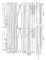
【解決手段】カラムAD変換部3は、カラムAD変換要素AとカラムAD変換要素Bとを備えている。カラムAD変換要素A,Bは、それぞれ、画素アレイ1から読み出した画素信号を上位2ビットの上位ブロックと下位2ビットの下位ブロックとの2つのブロックに分け、各ブロックを1水平走査期間単位で順次にAD変換する。制御部5は、カラムAD変換要素A,Bにそれぞれ異なる行の画素信号の異なるブロックのAD変換をオーバーラップして実行させ、ある1水平走査期間において、カラムAD変換要素j(j=A,B)に、第i(i=1〜8)行目の画素信号を読み出させた後、第i行目の画素信号の上位ブロックをAD変換させ、カラムAD変換要素k(k≠jかつ、k=A,B)に、第i−1行目の画素信号の下位ブロックをAD変換させる。
【選択図】図2
Description
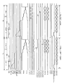
処理(1):Pixel readout(i行目):第i行目の画素信号を読み出し、CDS処理を行い、画素信号からノイズ信号を除去する。
処理(2):Upper bit A/D conversion(i行目):第i行目の画素信号の上位2ビットのAD変換を行う。
処理(3):Lower bit A/D conversion(i行目):第i行目の画素信号の下位2ビットのAD変換を行う。
処理(4):Column readout(i−1行目):AD変換された第i−1行目の画素信号を出力する。
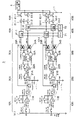
図1は、本発明の実施の形態1による固体撮像装置の全体構成図である。図1に示すように固体撮像装置は、列並列型AD変換方式のCMOSイメージセンサによる固体撮像装置であって、画素アレイ1、垂直走査回路2、カラムAD変換部(ADC)3、水平走査回路4、制御部5、画像処理部6、及び画像メモリ7を備えている。
次に、本発明の実施の形態2による固体撮像装置について説明する。実施の形態2による固体撮像装置は、カラムAD変換要素A,Bにラッチ回路41−1,41−2と、GCA部10Aとを共用させることを特徴とする。なお、本実施の形態において、実施の形態1と同一のものは同一の符号を用いて説明を省略する。
2 垂直走査回路
3 カラムAD変換部
4 水平走査回路
5 制御部
7 画像処理部
8 画像メモリ
10A,10B GCA部
20A,20B コンパレータ部
30A,30B ロジック回路
40A,40B ラッチ部
50A,50B スイッチ部
80A スイッチ部
Claims (7)
- 列並列型AD変換方式の固体撮像装置であって、
所定行×所定列のマトリックス状に配列された複数の画素から構成される画素アレイと、
前記画素アレイの各行をサイクリックに選択する垂直走査回路と、
前記画素アレイの各列に対応して設けられ、前記垂直走査回路により選択された行の画素信号を読み出し、AD変換するカラムAD変換部と、
制御部とを備え、
各列のカラムAD変換部は、第1〜第n(nは2以上の整数)のカラムAD変換要素を備え、
前記第1〜第nのカラムAD変換要素は、前記画素アレイから読み出した画素信号を最上位ビットから最下位ビットに向けて第1〜第nのブロックに分け、各ブロックを1水平走査期間単位で順次にAD変換し、
前記制御部は、前記第1〜第nのカラムAD変換要素に、それぞれ異なる行の画素信号の異なるブロックのAD変換をオーバーラップして実行させ、ある1水平走査期間において、第j(j=1〜n)のカラムAD変換要素に第i行目の画素信号を読み出させた後、前記第i行目の画素信号の第1のブロックをAD変換させることを特徴とする固体撮像装置。 - 前記制御部は、前記第jのカラムAD変換要素に、前記第i行目の画素信号を読み出させると同時に、前記第i行目よりもn行前に読み取った画素信号のAD変換後のデジタルデータを出力させることを特徴とする請求項1記載の固体撮像装置。
- 各カラムAD変換要素は、積分型のAD変換回路であることを特徴とする請求項1又は2記載の固体撮像装置。
- 前記第1〜第nのカラムAD変換要素は、
AD変換されたデジタルデータをラッチするラッチ部と、
前記ラッチ部によりラッチされたデジタルデータを伝送する水平信号線と前記ラッチ部との間に接続されたスイッチ部とを備え、
前記ラッチ部は、前記第1〜第nのブロックのデジタルデータをラッチするn個のラッチ回路を備え、
前記スイッチ部は、前記第1〜第nのブロックに対応するスイッチを備えることを特徴とする請求項3記載の固体撮像装置。 - 前記第1〜第nのカラムAD変換要素は、AD変換された画素信号をラッチするラッチ部を備え、
前記ラッチ部は、前記第1〜第nのブロックのデジタルデータをラッチし、前記第1〜第nのカラムAD変換要素に共用されるn個のラッチ回路を備えることを特徴とする請求項3記載の固体撮像装置。 - 各カラムAD変換要素は、
前記ラッチ部の前段に設けられたコンパレータと、
各カラムAD変換要素のコンパレータのうちいずれか1つのコンパレータと、n個のラッチ回路のうちいずれか1つのラッチ回路とを接続するスイッチ部とを備えることを特徴とする請求項5記載の固体撮像装置。 - 前記第1〜第nのカラムAD変換要素は、1つのGCA部を共用することを特徴とする請求項1〜6のいずれかに記載の固体撮像装置。
Priority Applications (2)
| Application Number | Priority Date | Filing Date | Title |
|---|---|---|---|
| JP2008163007A JP5077091B2 (ja) | 2008-06-23 | 2008-06-23 | 固体撮像装置 |
| US12/486,871 US8072527B2 (en) | 2008-06-23 | 2009-06-18 | Solid state image sensing device |
Applications Claiming Priority (1)
| Application Number | Priority Date | Filing Date | Title |
|---|---|---|---|
| JP2008163007A JP5077091B2 (ja) | 2008-06-23 | 2008-06-23 | 固体撮像装置 |
Publications (2)
| Publication Number | Publication Date |
|---|---|
| JP2010004440A true JP2010004440A (ja) | 2010-01-07 |
| JP5077091B2 JP5077091B2 (ja) | 2012-11-21 |
Family
ID=41430841
Family Applications (1)
| Application Number | Title | Priority Date | Filing Date |
|---|---|---|---|
| JP2008163007A Expired - Fee Related JP5077091B2 (ja) | 2008-06-23 | 2008-06-23 | 固体撮像装置 |
Country Status (2)
| Country | Link |
|---|---|
| US (1) | US8072527B2 (ja) |
| JP (1) | JP5077091B2 (ja) |
Families Citing this family (10)
| Publication number | Priority date | Publication date | Assignee | Title |
|---|---|---|---|---|
| JP5094498B2 (ja) * | 2008-03-27 | 2012-12-12 | キヤノン株式会社 | 固体撮像装置及び撮像システム |
| JP5332041B2 (ja) | 2009-03-13 | 2013-11-06 | ルネサスエレクトロニクス株式会社 | 固体撮像装置 |
| JP5762199B2 (ja) * | 2011-07-28 | 2015-08-12 | キヤノン株式会社 | 固体撮像装置 |
| JP2013090305A (ja) * | 2011-10-21 | 2013-05-13 | Sony Corp | 比較器、ad変換器、固体撮像装置、およびカメラシステム |
| US9843756B2 (en) | 2015-05-27 | 2017-12-12 | Samsung Electronics Co., Ltd. | Imaging devices, arrays of pixels receiving photocharges in bulk of select transistor, and methods |
| JP6727771B2 (ja) * | 2015-08-13 | 2020-07-22 | キヤノン株式会社 | 撮像装置 |
| KR101679598B1 (ko) * | 2016-01-04 | 2016-11-25 | 주식회사 동부하이텍 | 이미지 센서 |
| CN110771157B (zh) * | 2017-03-31 | 2022-02-08 | 普里露尼库斯新加坡私人有限公司 | 固态摄像装置、固态摄像装置的驱动方法、以及电子机器 |
| KR20190020408A (ko) * | 2017-08-21 | 2019-03-04 | 에스케이하이닉스 주식회사 | 고 선형성의 투-스텝 싱글-슬롭 비교 장치 및 그에 따른 씨모스 이미지 센서 |
| JP6929750B2 (ja) * | 2017-09-29 | 2021-09-01 | キヤノン株式会社 | 撮像装置、撮像システム、移動体 |
Citations (9)
| Publication number | Priority date | Publication date | Assignee | Title |
|---|---|---|---|---|
| JPH0548460A (ja) * | 1991-06-05 | 1993-02-26 | Matsushita Electric Ind Co Ltd | A/d変換器とこれを用いたセンサ及び3次元集積回路 |
| JP2002027331A (ja) * | 2000-07-03 | 2002-01-25 | Canon Inc | 信号処理装置、撮像装置及び撮像システム |
| JP2002232291A (ja) * | 2001-02-02 | 2002-08-16 | Riniaseru Design:Kk | アナログ−デジタル変換器及びこれを用いたイメージセンサ |
| JP2005347932A (ja) * | 2004-06-01 | 2005-12-15 | Canon Inc | 固体撮像装置および撮像システム |
| JP2007060401A (ja) * | 2005-08-25 | 2007-03-08 | Matsushita Electric Ind Co Ltd | イメージセンサー用アナログフロントエンド |
| JP2007336374A (ja) * | 2006-06-16 | 2007-12-27 | Canon Inc | 撮像装置及びその処理方法 |
| JP2008141610A (ja) * | 2006-12-04 | 2008-06-19 | Matsushita Electric Ind Co Ltd | 固体撮像装置及び撮像システム |
| JP2008167004A (ja) * | 2006-12-27 | 2008-07-17 | Sony Corp | 固体撮像装置、固体撮像装置の駆動方法および撮像装置 |
| JP2008236462A (ja) * | 2007-03-22 | 2008-10-02 | Seiko Epson Corp | 固体撮像素子用ad変換装置 |
Family Cites Families (6)
| Publication number | Priority date | Publication date | Assignee | Title |
|---|---|---|---|---|
| US4954897A (en) * | 1987-05-22 | 1990-09-04 | Nikon Corporation | Electronic still camera system with automatic gain control of image signal amplifier before image signal recording |
| US6873364B1 (en) * | 2000-06-08 | 2005-03-29 | Micron Technology, Inc. | Low-power signal chain for image sensors |
| US7129883B2 (en) * | 2004-02-23 | 2006-10-31 | Sony Corporation | Method and apparatus for AD conversion, semiconductor device for detecting distribution of physical quantity, and electronic apparatus |
| JP2006197393A (ja) * | 2005-01-14 | 2006-07-27 | Canon Inc | 固体撮像装置、カメラ、及び固体撮像装置の駆動方法 |
| US20060187329A1 (en) * | 2005-02-24 | 2006-08-24 | Micron Technology, Inc. | Clamped capacitor readout noise rejection circuit for imagers |
| US7825975B2 (en) * | 2008-02-25 | 2010-11-02 | Fairchild Imaging, Inc. | Imaging array with improved dynamic range |
-
2008
- 2008-06-23 JP JP2008163007A patent/JP5077091B2/ja not_active Expired - Fee Related
-
2009
- 2009-06-18 US US12/486,871 patent/US8072527B2/en not_active Expired - Fee Related
Patent Citations (9)
| Publication number | Priority date | Publication date | Assignee | Title |
|---|---|---|---|---|
| JPH0548460A (ja) * | 1991-06-05 | 1993-02-26 | Matsushita Electric Ind Co Ltd | A/d変換器とこれを用いたセンサ及び3次元集積回路 |
| JP2002027331A (ja) * | 2000-07-03 | 2002-01-25 | Canon Inc | 信号処理装置、撮像装置及び撮像システム |
| JP2002232291A (ja) * | 2001-02-02 | 2002-08-16 | Riniaseru Design:Kk | アナログ−デジタル変換器及びこれを用いたイメージセンサ |
| JP2005347932A (ja) * | 2004-06-01 | 2005-12-15 | Canon Inc | 固体撮像装置および撮像システム |
| JP2007060401A (ja) * | 2005-08-25 | 2007-03-08 | Matsushita Electric Ind Co Ltd | イメージセンサー用アナログフロントエンド |
| JP2007336374A (ja) * | 2006-06-16 | 2007-12-27 | Canon Inc | 撮像装置及びその処理方法 |
| JP2008141610A (ja) * | 2006-12-04 | 2008-06-19 | Matsushita Electric Ind Co Ltd | 固体撮像装置及び撮像システム |
| JP2008167004A (ja) * | 2006-12-27 | 2008-07-17 | Sony Corp | 固体撮像装置、固体撮像装置の駆動方法および撮像装置 |
| JP2008236462A (ja) * | 2007-03-22 | 2008-10-02 | Seiko Epson Corp | 固体撮像素子用ad変換装置 |
Also Published As
| Publication number | Publication date |
|---|---|
| US20090316034A1 (en) | 2009-12-24 |
| US8072527B2 (en) | 2011-12-06 |
| JP5077091B2 (ja) | 2012-11-21 |
Similar Documents
| Publication | Publication Date | Title |
|---|---|---|
| JP5077091B2 (ja) | 固体撮像装置 | |
| EP1655840B1 (en) | Analog-to-digital conversion method, analog-to-digital converter, semiconductor device for detecting distribution of physical quantity, and electronic apparatus | |
| US8462246B2 (en) | Apparatus and method for CDS and ADC with multiple samplings in image sensor | |
| US6885331B2 (en) | Ramp generation with capacitors | |
| US9450596B2 (en) | Ramp and successive approximation register analog to digital conversion methods, systems and apparatus | |
| CN104115211B (zh) | 高动态范围成像系统 | |
| US8665354B2 (en) | Solid-state image pickup device | |
| KR20190020408A (ko) | 고 선형성의 투-스텝 싱글-슬롭 비교 장치 및 그에 따른 씨모스 이미지 센서 | |
| JP2011526088A (ja) | 改善されたダイナミックレンジを有するイメージング配列 | |
| US10097781B2 (en) | Analog-to-digital converter and operating method thereof | |
| US9848154B2 (en) | Comparator with correlated double sampling scheme and operating method thereof | |
| US20190158772A1 (en) | Single-slope comparison device with low-noise, and analog-to-digital conversion device and cmos image sensor including the same | |
| US20090295453A1 (en) | Signal reading method, signal reading circuit, and image sensor | |
| US8558729B2 (en) | Solid-state imaging apparatus | |
| US10715757B2 (en) | A/D converter | |
| KR20160145217A (ko) | 카운팅 회로, 그 카운팅 회로를 포함하는 이미지 센싱 장치 및 그 이미지 센싱 장치의 리드아웃 방법 | |
| JP5749579B2 (ja) | Ad変換回路および固体撮像装置 | |
| JP2010004439A (ja) | 固体撮像装置 | |
| KR20120053456A (ko) | 엑스선 이미지 센서 시스템용 병렬 처리 독출 회로 및 독출 방법 | |
| WO2019092805A1 (ja) | 増幅回路及びそれを備えるアナログデジタル変換システム | |
| JP3576073B2 (ja) | 固体撮像装置 | |
| JP4478798B2 (ja) | オフセット低減機能をもつ巡回型a/d変換器、およびオフセット電圧を低減する方法 | |
| JP6012829B2 (ja) | 固体撮像装置 | |
| CN116419086B (zh) | 比较器、图像传感器读出电路及读出方法 | |
| JP2014120987A (ja) | A/d変換回路および固体撮像装置 |
Legal Events
| Date | Code | Title | Description |
|---|---|---|---|
| A621 | Written request for application examination |
Free format text: JAPANESE INTERMEDIATE CODE: A621 Effective date: 20110215 |
|
| A977 | Report on retrieval |
Free format text: JAPANESE INTERMEDIATE CODE: A971007 Effective date: 20120724 |
|
| TRDD | Decision of grant or rejection written | ||
| A01 | Written decision to grant a patent or to grant a registration (utility model) |
Free format text: JAPANESE INTERMEDIATE CODE: A01 Effective date: 20120731 |
|
| A01 | Written decision to grant a patent or to grant a registration (utility model) |
Free format text: JAPANESE INTERMEDIATE CODE: A01 |
|
| A61 | First payment of annual fees (during grant procedure) |
Free format text: JAPANESE INTERMEDIATE CODE: A61 Effective date: 20120813 |
|
| FPAY | Renewal fee payment (event date is renewal date of database) |
Free format text: PAYMENT UNTIL: 20150907 Year of fee payment: 3 |
|
| R150 | Certificate of patent or registration of utility model |
Free format text: JAPANESE INTERMEDIATE CODE: R150 |
|
| S111 | Request for change of ownership or part of ownership |
Free format text: JAPANESE INTERMEDIATE CODE: R313111 |
|
| R350 | Written notification of registration of transfer |
Free format text: JAPANESE INTERMEDIATE CODE: R350 |
|
| LAPS | Cancellation because of no payment of annual fees |