JP2010004440A - Solid-state image pickup device - Google Patents
Solid-state image pickup device Download PDFInfo
- Publication number
- JP2010004440A JP2010004440A JP2008163007A JP2008163007A JP2010004440A JP 2010004440 A JP2010004440 A JP 2010004440A JP 2008163007 A JP2008163007 A JP 2008163007A JP 2008163007 A JP2008163007 A JP 2008163007A JP 2010004440 A JP2010004440 A JP 2010004440A
- Authority
- JP
- Japan
- Prior art keywords
- column
- conversion
- row
- pixel signal
- unit
- Prior art date
- Legal status (The legal status is an assumption and is not a legal conclusion. Google has not performed a legal analysis and makes no representation as to the accuracy of the status listed.)
- Granted
Links
Images


Classifications
-
- H—ELECTRICITY
- H04—ELECTRIC COMMUNICATION TECHNIQUE
- H04N—PICTORIAL COMMUNICATION, e.g. TELEVISION
- H04N25/00—Circuitry of solid-state image sensors [SSIS]; Control thereof
- H04N25/70—SSIS architectures; Circuits associated therewith
- H04N25/71—Charge-coupled device [CCD] sensors; Charge-transfer registers specially adapted for CCD sensors
- H04N25/75—Circuitry for providing, modifying or processing image signals from the pixel array
-
- H—ELECTRICITY
- H04—ELECTRIC COMMUNICATION TECHNIQUE
- H04N—PICTORIAL COMMUNICATION, e.g. TELEVISION
- H04N25/00—Circuitry of solid-state image sensors [SSIS]; Control thereof
- H04N25/70—SSIS architectures; Circuits associated therewith
- H04N25/76—Addressed sensors, e.g. MOS or CMOS sensors
Abstract
Description
本発明は、列並列型AD変換方式の固体撮像装置に関するものである。 The present invention relates to a column parallel AD conversion type solid-state imaging device.
近年、列並列型AD変換方式のCMOSイメージセンサによる固体撮像装置が広く普及している。この固体撮像装置は、例えば、所定行×所定列のマトリックス状に配列された複数の画素から構成される画素アレイと、画素アレイの各列に対応して設けられ、画素アレイから画素信号を読み出してAD変換するカラムAD変換回路とを備えている。そして、カラムAD変換回路として、画素信号を2つのブロックに分けてAD変換する2回積分型のAD変換回路を採用する固体撮像装置が知られている(特許文献1)。 In recent years, solid-state imaging devices using column parallel AD conversion type CMOS image sensors have been widely used. This solid-state imaging device is provided corresponding to each column of the pixel array, for example, which includes a plurality of pixels arranged in a matrix of predetermined rows × predetermined columns, and reads out pixel signals from the pixel array And a column AD conversion circuit for AD conversion. As a column AD conversion circuit, there is known a solid-state imaging device that employs a double integration type AD conversion circuit that performs AD conversion by dividing a pixel signal into two blocks (Patent Document 1).
図9は、従来の固体撮像装置に採用されるカラムAD変換回路の1列分の回路図を示している。図9に示すカラムAD変換回路は、シングルスロープ積分型のカラムAD変換回路であり、画素アレイからの画素信号が入力される上段から順に、GCA(Gain Control Amp)部100、コンパレータ部200、ロジック回路300、ラッチ部400、及びスイッチ部500を備えている。
FIG. 9 shows a circuit diagram for one column of a column AD conversion circuit employed in a conventional solid-state imaging device. The column AD conversion circuit shown in FIG. 9 is a single slope integration type column AD conversion circuit, and in order from the upper stage to which a pixel signal from the pixel array is input, a GCA (Gain Control Amp)
GCA部100は、画素アレイから出力された画素信号に対して、CDS(Correlated Double Sampling:相関2重サンプリング)処理を行いながら増幅し、画像信号からノイズ信号を除去する。
The
コンパレータ部200は、2段のコンパレータを備え、GCA部100から出力された画素信号を2つのランプ信号(以下、Ramp1,Ramp2と称する。)と比較する。ここで、Ramp1は、時間が経過するにつれて4段階で段階的に減少し、Ramp2は、時間が経過するにつれて4段階で段階的に増大する。
The
そして、コンパレータ部200は、GCA部100から出力された画素信号の上位2ビット分をAD変換するために、当該画素信号とRamp1とを比較し、Ramp1のレベルが画素信号のレベルを下回ったとき、出力信号を反転させる。Ramp1と画素信号との比較が終了すると、コンパレータ部200は、GCA部100から出力された画素信号の下位2ビット分をAD変換するために、当該画素信号とRamp2とを比較し、Ramp2のレベルが当該画素信号のレベルを上回ったとき、出力信号を反転させる。
Then, the
ロジック回路300は、画素信号とRamp1との比較によりコンパレータ部200の出力信号が反転されたとき、COMPOUT1=L(ローレベル)にしてラッチ回路410に出力する。また、ロジック回路300は、画素信号とRamp2との比較によりコンパレータ部200の出力信号が反転されたとき、COMPOUT2=Lにしてラッチ回路420に出力する。
When the output signal of the
カウンタ710は、カラムAD変換回路の外に設けられた2ビットのカウンタから構成され、Ramp1がコンパレータ部200に入力されたとき、カウント動作を開始する。また、カウンタ720は、カラムAD変換回路の外に設けられた2ビットのカウンタから構成され、Ramp2がコンパレータ部200に入力されたとき、カウント動作を開始する。
The
ラッチ部400は、ラッチ回路410及びラッチ回路420を備える。ラッチ回路410は、COMPOUT1=Lとなったとき、カウンタ710の現在のカウント値をラッチする。これにより、ラッチ回路410は、AD変換された画素信号の上位2ビットのデジタルデータをラッチする。
The
また、ラッチ回路420は、COMPOUT2=Lになったとき、カウンタ720のカウント値をラッチする。これにより、ラッチ回路420は、AD変換された画素信号の下位2ビットのデジタルデータをラッチする。
The
水平走査回路600は、画素信号の上位2ビットと下位2ビットとのAD変換が終了すると、各列を順次選択するための列選択信号をスイッチ510,520に出力して、スイッチ510,520をオンさせて、ラッチ回路410にラッチされた上位2ビットのデジタルデータと、ラッチ回路420にラッチされた下位2ビットのデジタルデータとを水平信号線に出力させる。
When the AD conversion of the upper 2 bits and the lower 2 bits of the pixel signal is completed, the
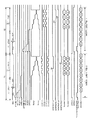
図10は、図9に示すカラムAD変換回路のタイミングチャートを示している。このタイミングチャートは、ある1水平走査期間(1H Period)において、画素アレイの第i行目の画素信号に対する処理が示されている。 FIG. 10 shows a timing chart of the column AD conversion circuit shown in FIG. This timing chart shows processing for a pixel signal in the i-th row of the pixel array in a certain horizontal scanning period (1H period).
また、図10に示すvpixelはGCA部100に入力される画素信号を示し、φPRSTはGCA部100のスイッチをオン・オフする信号を示し、φS1はコンパレータ部200の前段のコンパレータのスイッチをオン・オフする信号を示し、φS2はコンパレータ部200の後段のコンパレータのスイッチをオン・オフする信号を示し、φSHはGCA部100とコンパレータ部200との間に接続されたスイッチをオン・オフする信号を示し、φCK1はロジック回路300の1段目の上側のNANDゲートに入力される信号を示し、φCK2はロジック回路300の1段目の下側のNANDゲートに入力される信号を示し、Counter1はカウンタ710のカウント値を示し、Counter2はカウンタ720のカウント値を示し、Horizontal Shift Resister Start Pulseは1水平走査期間の開始を示す水平同期信号を示し、DATAOUTはラッチ回路410,420から出力されるデジタルデータを示している。
Further, vpixel shown in FIG. 10 indicates a pixel signal input to the
図10に示すように、1水平走査期間において、以下の処理(1)〜処理(3)の3つの処理が実行され、また、処理(1)〜処理(3)と並行して以下の処理(4)が実行される。
処理(1):Pixel readout(i行目):第i行目の画素信号を読み出し、CDS処理を行い、画素信号からノイズ信号を除去する。
処理(2):Upper bit A/D conversion(i行目):第i行目の画素信号の上位2ビットのAD変換を行う。
処理(3):Lower bit A/D conversion(i行目):第i行目の画素信号の下位2ビットのAD変換を行う。
処理(4):Column readout(i−1行目):AD変換された第i−1行目の画素信号を出力する。
As shown in FIG. 10, the following three processes (1) to (3) are executed in one horizontal scanning period, and the following processes are performed in parallel with the processes (1) to (3). (4) is executed.
Process (1): Pixel readout (i-th row): The pixel signal on the i-th row is read out, CDS processing is performed, and a noise signal is removed from the pixel signal.
Process (2): Upper bit A / D conversion (i-th row): AD conversion of the upper 2 bits of the pixel signal on the i-th row is performed.
Process (3): Lower bit A / D conversion (i-th row): AD conversion of lower 2 bits of the pixel signal of the i-th row is performed.
Process (4): Column readout (i-1 line): The pixel signal of the i-1th line after AD conversion is output.
図9に示すようにラッチ部400がラッチ回路410,420による2段構成となっているため、上記処理(1)〜処理(3)と、処理(4)とを並行して行うことができる。すなわち第i行目の画像信号をAD変換しながら、第i−1行目の画素信号のデジタルデータを読み出すことができる。
As shown in FIG. 9, since the
処理(2)の期間のタイミングTM1において、ランプ信号Ramp1のレベルが画素信号のレベルを下回ったとき、COMPOUT1=Lとなる。そして、COMPOUT1=LとなったときのCounter1のカウント値が「01」であるため、ラッチ回路410は「01」をラッチする。また、処理(3)の期間のタイミングTM2において、ランプ信号Ramp2のレベルが画素信号のレベルを上回ったとき、COMPOUT2=Lとなる。そして、COMPOUT2=LとなったときのCounter2のカウント値が「10」であるため、ラッチ回路420は「10」をラッチする。
When the level of the ramp signal Ramp1 falls below the level of the pixel signal at the timing TM1 in the period of the process (2), COMPOUT1 = L. Since the count value of Counter1 when COMPOUT1 = L is “01”, the
そして、次の1水平走査期間において、ラッチ回路410にラッチされた「01」とラッチ回路420にラッチされた「10」とが、水平信号線に出力される。
In the next horizontal scanning period, “01” latched by the
このような2回積分型のAD変換回路は少ないクロック数でAD変換をすることができ、1回積分型のAD変換回路に比べてAD変換に必要な時間が少なくなって1水平走査期間を短縮し、フレームレートを上げ、より高速な撮影が可能になるという特徴を持っている。 Such a double integration type AD converter circuit can perform AD conversion with a small number of clocks, and the time required for AD conversion is reduced as compared with the single integration type AD conversion circuit. It has the characteristics of shortening, increasing the frame rate, and enabling higher-speed shooting.
図11は、図9に示す第i行目と第i+1行目との画素信号に対するAD変換回路のシーケンス図を示している。1段目の1水平走査期間において、処理(1)〜処理(3)が実行され、第i行目の画素信号がA/D変換され、ラッチ回路410,420にラッチされる。
FIG. 11 shows a sequence diagram of the AD conversion circuit for the pixel signals of the i-th row and the (i + 1) -th row shown in FIG. In the first horizontal scanning period of the first stage, processing (1) to processing (3) are executed, and the pixel signal of the i-th row is A / D converted and latched in the
2段目の1水平走査期間において、処理(1)〜処理(3)が実行され、第i+1行目の画素信号がA/D変換され、ラッチ回路410,420にラッチされ、かつ、処理(4)が実行され、ラッチされた第i行目のデジタルデータがラッチ回路410,420から出力される。
In the second horizontal scanning period, the processing (1) to processing (3) are executed, the pixel signals in the (i + 1) th row are A / D converted, latched in the
3段目の1水平走査期間において、処理(4)が実行され、ラッチされた第i+1行目のデジタルデータがラッチ回路410,420から出力される。
In the third horizontal scanning period, the process (4) is executed, and the latched digital data in the (i + 1) th row are output from the
すなわち、各1水平走査期間において、第i+1行目の画素信号のAD変換処理と、第i−1行目の画素信号の出力処理とがオーバーラップして実行される。 That is, in each horizontal scanning period, the AD conversion processing of the pixel signal of the (i + 1) th row and the output processing of the pixel signal of the (i-1) th row are executed in an overlapping manner.
ところで、図9に示すAD変換回路のように、画素信号を上位2ビットと下位2ビットとに分割してAD変換する場合、上位2ビットのデジタルデータの結果が重要となる。上位2ビットのAD変換は、Ramp1と画素信号とを比較することで実行されるが、Ramp1が完全にセトリングするためにはある程度の時間が必要となる。そのため、上位2ビットのAD変換を高精度に行うためには、上位2ビットのAD変換の期間を一定時間以上確保する必要がある。
しかしながら、図9に示すAD変換回路では、図11に示すように1水平走査期間内において処理(1)〜処理(3)が実行されている。一方、上位2ビットをAD変換する処理(2)の時間を短くすることは困難である。そのため、1水平走査期間を短縮することができず、フレームレートを上げることができないという問題があった。 However, in the AD conversion circuit shown in FIG. 9, the processes (1) to (3) are executed within one horizontal scanning period as shown in FIG. On the other hand, it is difficult to shorten the time of the process (2) for AD converting the upper 2 bits. Therefore, there is a problem that one horizontal scanning period cannot be shortened and the frame rate cannot be increased.
本発明の目的は、1水平走査期間を短縮してフレームレートの高速化を図っても、高精度なAD変換を実現することができる固体撮像装置を提供することである。 An object of the present invention is to provide a solid-state imaging device capable of realizing highly accurate AD conversion even if the frame rate is increased by shortening one horizontal scanning period.
(1)本発明による固体撮像装置は、列並列型AD変換方式の固体撮像装置であって、所定行×所定列のマトリックス状に配列された複数の画素から構成される画素アレイと、前記画素アレイの各行をサイクリックに選択する垂直走査回路と、前記画素アレイの各列に対応して設けられ、前記垂直走査回路により選択された行の画素信号を読み出し、AD変換するカラムAD変換部と、制御部とを備え、各列のカラムAD変換部は、第1〜第n(nは2以上の整数)のカラムAD変換要素を備え、前記第1〜第nのカラムAD変換要素は、前記画素アレイから読み出した画素信号を最上位ビットから最下位ビットに向けて第1〜第nのブロックに分け、各ブロックを1水平走査期間単位で順次にAD変換し、前記制御部は、前記第1〜第nのカラムAD変換要素に、それぞれ異なる行の画素信号の異なるブロックのAD変換をオーバーラップして実行させ、ある1水平走査期間において、第j(j=1〜n)のカラムAD変換要素に第i行目の画素信号を読み出させた後、前記第i行目の画素信号の第1のブロックをAD変換させることを特徴とする。 (1) A solid-state imaging device according to the present invention is a column-parallel AD conversion type solid-state imaging device, and includes a pixel array composed of a plurality of pixels arranged in a matrix of predetermined rows × predetermined columns, and the pixels A vertical scanning circuit that cyclically selects each row of the array, and a column AD conversion unit that is provided corresponding to each column of the pixel array and that reads a pixel signal of the row selected by the vertical scanning circuit and performs AD conversion; , A column AD conversion unit for each column includes first to nth (n is an integer of 2 or more) column AD conversion elements, and the first to nth column AD conversion elements are: The pixel signal read from the pixel array is divided into first to n-th blocks from the most significant bit to the least significant bit, and each block is sequentially AD converted in units of one horizontal scanning period. 1st to nth The ram AD conversion element causes the AD conversion of different blocks of pixel signals in different rows to overlap each other, and in a certain horizontal scanning period, the jth (j = 1 to n) column AD conversion elements are After the pixel signal of the row is read out, the first block of the pixel signal of the i-th row is AD converted.
この構成によれば、第1〜第nのカラムAD変換要素は、画素信号を最上位ビットから最下位ビットに向けて第1〜第nのブロックに分け、各ブロックの画素信号を1水平走査期間単位で順次にAD変換する。 According to this configuration, the first to nth column AD conversion elements divide the pixel signal into the first to nth blocks from the most significant bit to the least significant bit, and perform one horizontal scan on the pixel signal of each block. AD conversion is sequentially performed in units of periods.
また、制御部は、第1〜第nのカラムAD変換要素に、それぞれ異なる行の画素信号の異なるブロックのAD変換をオーバーラップして実行させる。このとき、制御部は、ある1水平走査期間において、第j(j=1〜n)のカラムAD変換要素に第i行目の画素信号を読み出させた後、第i行目の画素信号の第1のブロックをAD変換させる。 Further, the control unit causes the first to nth column AD conversion elements to overlap and execute AD conversion of different blocks of pixel signals in different rows. At this time, in a certain horizontal scanning period, the control unit causes the j-th (j = 1 to n) column AD conversion element to read the pixel signal of the i-th row, and then the pixel signal of the i-th row. AD conversion is performed on the first block.
したがって、1水平走査期間において、第i行目の画素信号の読み取り処理と、第i行目の画素信号の第1のブロックのAD変換処理との2つの処理のみが行われ、従来のように画素信号を読み出す処理と、読み出した画素信号の上位2ビットをAD変換する処理と、読み出した画素信号の下位2ビットをAD変換する処理とが同時に実行されないため、第1のブロックの画素信号のAD変換処理の期間を一定時間以上確保することが可能となり、第1のブロックの画素信号を高精度にAD変換することができ、かつ、1水平走査期間を短縮化することができる。 Therefore, in one horizontal scanning period, only two processes of the reading process of the pixel signal of the i-th row and the AD conversion process of the first block of the pixel signal of the i-th row are performed. Since the process of reading the pixel signal, the process of AD converting the upper 2 bits of the read pixel signal, and the process of AD converting the lower 2 bits of the read pixel signal are not performed simultaneously, the pixel signal of the first block A period of AD conversion processing can be secured for a certain time or more, the pixel signal of the first block can be AD converted with high accuracy, and one horizontal scanning period can be shortened.
よって、1水平走査期間を短縮してフレームレートの高速化を図っても、高精度なAD変換を実現することができる。 Therefore, even if the horizontal scanning period is shortened to increase the frame rate, highly accurate AD conversion can be realized.
(2)前記制御部は、前記第jのカラムAD変換要素に、前記第i行目の画素信号を読み出させると同時に、前記第i行目よりもn行前に読み取った画素信号のAD変換後のデジタルデータを出力させることが好ましい。 (2) The control unit causes the j-th column AD conversion element to read the pixel signal of the i-th row, and at the same time, the AD of the pixel signal read n rows before the i-th row It is preferable to output the converted digital data.
この構成によれば、AD変換された1行のデジタルデータを、1水平走査期間単位で出力することができる。 According to this configuration, one row of digital data subjected to AD conversion can be output in units of one horizontal scanning period.
(3)各カラムAD変換要素は、積分型のAD変換回路であることが好ましい。 (3) Each column AD conversion element is preferably an integral AD conversion circuit.
この構成によれば、各AD変換要素が積分型のAD変換回路により構成されているため、高精度なAD変換を実現することができる。 According to this configuration, since each AD conversion element is configured by an integral AD conversion circuit, highly accurate AD conversion can be realized.
(4)前記第1〜第nのカラムAD変換要素は、AD変換されたデジタルデータをラッチするラッチ部と、前記ラッチ部によりラッチされたデジタルデータを伝送する水平信号線と前記ラッチ部との間に接続されたスイッチ部とを備え、前記ラッチ部は、前記第1〜第nのブロックのデジタルデータをラッチするn個のラッチ回路を備え、前記スイッチ部は、前記第1〜第nのブロックに対応するスイッチを備えることが好ましい。 (4) The first to nth column AD conversion elements include: a latch unit that latches AD-converted digital data; a horizontal signal line that transmits the digital data latched by the latch unit; and the latch unit A switch unit connected in between, wherein the latch unit includes n latch circuits that latch digital data of the first to n-th blocks, and the switch unit includes the first to n-th blocks. It is preferable to provide a switch corresponding to the block.
この構成によれば、スイッチ部は、第1〜第nのブロックのデジタルデータを、ラッチ部から水平信号線に順次に出力することができる。 According to this configuration, the switch unit can sequentially output the digital data of the first to nth blocks from the latch unit to the horizontal signal line.
(5)前記第1〜第nのカラムAD変換要素は、AD変換された画素信号をラッチするラッチ部を備え、前記ラッチ部は、前記第1〜第nのブロックのデジタルデータをラッチし、前記第1〜第nのカラムAD変換要素に共用されるn個のラッチ回路を備えることが好ましい。 (5) The first to n-th column AD conversion elements include a latch unit that latches AD-converted pixel signals, and the latch unit latches the digital data of the first to n-th blocks, It is preferable that n latch circuits shared by the first to nth column AD conversion elements are provided.
この構成によれば、第1〜第nのブロックに対応するn個のラッチ回路が、第1〜第nのカラムAD変換要素に共用されるため、回路規模の縮小を図ることができる。 According to this configuration, since the n latch circuits corresponding to the first to nth blocks are shared by the first to nth column AD conversion elements, the circuit scale can be reduced.
(6)各カラムAD変換要素は、前記ラッチ部の前段に設けられたコンパレータと、各カラムAD変換要素のコンパレータのうちいずれか1つのコンパレータと、n個のラッチ回路のうちいずれか1つのラッチ回路とを接続するスイッチ部とを備えることが好ましい。 (6) Each column AD conversion element includes any one of the comparators provided in the preceding stage of the latch unit, the comparator of each column AD conversion element, and any one of the n latch circuits. It is preferable to include a switch unit that connects the circuit.
この構成によれば、コンパレータとラッチ回路との間にスイッチ部が設けられているため、第1〜第nのカラムAD変換要素にラッチ回路を共用させた場合であっても、各ラッチ回路に、対応するブロックのデジタルデータをラッチさせることができる。 According to this configuration, since the switch unit is provided between the comparator and the latch circuit, each latch circuit can be used even when the first to nth column AD conversion elements share the latch circuit. The digital data of the corresponding block can be latched.
(7)前記第1〜第nのカラムAD変換要素は、1つのGCA部を共用することが好ましい。 (7) It is preferable that the first to nth column AD conversion elements share one GCA unit.
この構成によれば、第1〜第nのカラムAD変換要素は1つのGCA部を共用するため、回路規模の縮小を図ることができる。 According to this configuration, since the first to nth column AD conversion elements share one GCA unit, the circuit scale can be reduced.
本発明によれば、1水平走査期間を短縮してフレームレートの高速化を図っても、高精度なAD変換を実現することができる。 According to the present invention, highly accurate AD conversion can be realized even if the frame rate is increased by shortening one horizontal scanning period.
(実施の形態1)
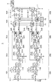
図1は、本発明の実施の形態1による固体撮像装置の全体構成図である。図1に示すように固体撮像装置は、列並列型AD変換方式のCMOSイメージセンサによる固体撮像装置であって、画素アレイ1、垂直走査回路2、カラムAD変換部(ADC)3、水平走査回路4、制御部5、画像処理部6、及び画像メモリ7を備えている。
(Embodiment 1)
FIG. 1 is an overall configuration diagram of a solid-state imaging device according to
画素アレイ1は、複数の画素が8行×8列でマトリックス状に配列されている。なお、8行×8列は一例であり、M(Mは2以上の正の整数)行×N(Nは2以上の正の整数)列に配列してもよい。
In the
垂直走査回路2は、例えば、シフトレジスタを含み、画素アレイ1の第1行目〜第8行目の各行に対応する8本の画素制御線HL1を介して画素アレイ1と接続されている。そして、垂直走査回路2は、垂直同期信号VDに同期して、第1行目〜第8行目の画素制御線HL1をサイクリックに選択することで、画素アレイ1を垂直走査する。
The
カラムAD変換部3は、画素アレイ1の各列に対応して8個設けられている。各カラムAD変換部3は、画素アレイ1の第1列目〜第8列目の各列に対応する8本の垂直信号線VL1を介して画素アレイ1と接続され、垂直走査回路2の垂直走査により選択された行において、対応する各列の画素から画素信号を読み出し、CDS処理及びAD変換を施す。
Eight
本実施の形態では、カラムAD変換部3は、カラムAD変換要素AとカラムAD変換要素Bとの2つのカラムAD変換要素を備えている。そして、カラムAD変換要素A,Bは、それぞれ、画素信号を最上位ビットから最下位ビットに向けて2つのブロックに分け、各ブロックを1水平走査期間単位で順次にAD変換する2回積分型のAD変換回路により構成されている。
In the present embodiment, the column
水平走査回路4は、シフトレジスタを備え、水平同期信号HDに同期して列選択信号線を出力することで、1水平走査期間において、第1列目〜第8列目のカラムAD変換部3をサイクリックに選択してカラムAD変換部3を水平走査し、カラムAD変換部3が保持する第1列目〜第8列目の画素信号を順次に出力させる。
The
制御部5は、CPU(中央演算処理装置)、ROM(リードオンリーメモリ)、及びRAM(ランダムアクセスメモリ)等かなるマイコンから構成され、固体撮像装置全体制御を司る。 The control unit 5 includes a microcomputer including a CPU (Central Processing Unit), a ROM (Read Only Memory), and a RAM (Random Access Memory), and controls the entire solid-state imaging device.
ここで、制御部5は、カラムAD変換要素A,Bにそれぞれ異なる行の画素信号の異なるブロックのAD変換をオーバーラップして実行させ、ある1水平走査期間において、カラムAD変換要素j(j=A,B)に、第i(i=1〜8)行目の画素信号を読み出させた後、第i行目の画素信号の上位ブロックをAD変換させ、カラムAD変換要素k(k≠jかつ、k=A,B)に、第i−1行目の画素信号の下位ブロックをAD変換させる。 Here, the control unit 5 causes the column AD conversion elements A and B to execute the AD conversion of the different blocks of the pixel signals in different rows so as to overlap each other, and in a certain horizontal scanning period, the column AD conversion element j (j = A, B), after reading out the pixel signals of the i-th (i = 1 to 8) rows, the upper block of the pixel signals of the i-th row is AD-converted, and the column AD conversion element k (k ≠ j and k = A, B), the lower block of the pixel signal in the (i−1) th row is AD converted.
また、制御部5は、カラムAD変換要素jに、第i行目の画素信号を読み出させると同時に、第n−2行目の画素信号のデジタルデータを出力させる。 In addition, the control unit 5 causes the column AD conversion element j to read out the pixel signal of the i-th row and simultaneously output the digital data of the pixel signal of the n-2th row.
画像処理部6は、各カラムAD変換部3から出力されたデジタルデータからなる画像データに種々の画像処理を施す。画像メモリ7は、ハードディスク等の記憶装置から構成され、画像処理部6により所定の画像処理が行われた画像データを記憶する。
The
図2は、カラムAD変換部3の回路図を示している。図2において、カラムAD変換要素Aに示されるφCOL_A,φPRST_A,φSH_A,φS1_A,φS2_A,φCK1_A,φCK2_A,XφPRST_A,φRD_Aは制御信号を示し、それぞれ、制御部5から出力される。また、カラムAD変換要素Bに示されるφCOL_B,φPRST_B,φSH_B,φS1_B,φS2_B,φCK1_B,φCK2_B,XφPRST_B,φRD_Bは、制御信号を示し、それぞれ、制御部5から出力される。また、Ramp1,Ramp2はランプ信号を示し、それぞれ制御部5から出力される。
FIG. 2 shows a circuit diagram of the column
カラムAD変換要素Aは、GCA(Gain Control Amp)部10A、コンパレータ部20A、ロジック回路30A、ラッチ部40A、及びスイッチ部50Aを備えている。
The column AD conversion element A includes a GCA (Gain Control Amp)
GCA部10Aは、画素アレイ1から出力された画素信号に対して、CDS処理を行いながら増幅処理を行い、画素信号からノイズ信号を除去する。
The
具体的にはGCA部10Aは、GCAアンプ11Aと、GCAアンプ11Aの−端子に接続されたコンデンサC1Aと、GCAアンプ11Aの出力端子と−端子との間に接続されたコンデンサC2Aと、コンデンサC2Aに並列接続されたスイッチSW11Aと、コンデンサC2Aと垂直信号線VL1との間に接続されたスイッチSW12Aとを備えている。
Specifically, the
ここで、コンデンサC1A,C2Aの容量比で定められるゲインにより画素信号は増幅される。また、コンデンサC2Aは、スイッチSW11Aがオン・オフによりリセットされる。スイッチSW12A,SW11Aは、それぞれ、φCOL_A,φPRST_Aによって、オン・オフされる。 Here, the pixel signal is amplified by a gain determined by the capacitance ratio of the capacitors C1A and C2A. The capacitor C2A is reset when the switch SW11A is turned on / off. The switches SW12A and SW11A are turned on / off by φCOL_A and φPRST_A, respectively.
コンパレータ部20Aは、2段のコンパレータ21A及び22Aを備え、GCA部10Aから出力された画素信号をRamp1,Ramp2と比較する。本実施の形態では、画素信号は、上位2ビットの上位ブロックと下位2ビットの下位ブロックとの2つのブロックに分けてAD変換される。そのため、Ramp1は上位ブロックをAD変換するために、4(=22)段階で段階的に減少するランプ信号が採用され、Ramp2は下位ブロックをAD変換するために、4(=22)段階で段階的に増大するランプ信号が採用される。
The
そして、コンパレータ部20Aは、GCA部10Aから出力された画素信号の上位ブロックをAD変換するために、当該画素信号とRamp1とを比較し、Ramp1のレベルが画素信号のレベルを下回ったとき、出力信号を反転させる。
Then, the
また、コンパレータ部20Aは、Ramp1と画素信号との比較が終了すると、GCA部10Aから出力された画素信号の下位ブロックをAD変換するために、当該画素信号とRamp2とを比較し、Ramp2のレベルが当該画素信号のレベルを上回ったとき、出力信号を反転させる。
When the comparison between Ramp1 and the pixel signal is completed, the
具体的には、コンパレータ部20Aは、コンパレータ21Aの−端子に接続されたコンデンサC3Aと、コンデンサC3AとGCAアンプ11Aとの間に接続されたスイッチSW21Aと、コンパレータ21Aの+端子に接続されたスイッチSW22Aと、コンパレータ21Aの+端子に接続され、Ramp2が入力されるコンデンサC4Aと、一端がコンパレータ21Aの+端子に接続され、他端が接地されたたコンデンサC5Aと、コンパレータ21Aの−端子と出力端子との間に接続されたスイッチSW23Aと、コンパレータ21Aとコンパレータ22Aとの間に接続されたコンデンサC6Aと、コンパレータ22Aの入力端子と出力端子との間に接続されたスイッチSW24Aとを備えている。
Specifically, the
コンパレータ21Aは、差動コンパレータにより構成され、+端子に入力されるRamp1又はRamp2と画素信号とを比較する。コンパレータ22Aは、シングルエンドコンパレータにより構成され、コンパレータ21Aからの出力信号を所定の値と比較する。
The
スイッチSW21A,SW23A,SW24Aは、φSH_A,φS1_A,φS2_Aに従って、オン・オフする。また、スイッチSW22Aは、ロジック回路30Aから出力されるCOMPOUT1_Aに従って、オン・オフする。
The switches SW21A, SW23A, and SW24A are turned on / off according to φSH_A, φS1_A, and φS2_A. The switch SW22A is turned on / off according to COMPOUT1_A output from the
ロジック回路30Aは、画素信号とRamp1との比較によりコンパレータ部20Aからの出力信号が反転されたとき、COMPOUT1_A=Lとし、ラッチ回路41−1にカウンタ71の現在のカウント値をラッチさせる。これにより、上位ブロックのデジタルデータが得られる。また、ロジック回路30Aは、画素信号とRamp2との比較によりコンパレータ22Aからの出力信号が反転されたとき、COMPOUT2_A=Lとし、ラッチ回路41−2に出力し、ラッチ回路41−2にカウンタ72の現在のカウント値をラッチさせる。これにより下位ブロックのデジタルデータが得られる。
When the output signal from the
具体的には、ロジック回路30Aは、一方の入力端子がコンパレータ22Aに接続され、他方の入力端子にφCK1_Aが入力されるNANDゲート31Aと、一方の入力端子がNOTゲート37Aを介してコンパレータ22Aに接続され、他方の入力端子にφCK2_Aが入力されるNANDゲート32Aと、NANDゲート31Aとラッチ回路41−1との間に接続されたR−Sフリップフロップ33Aと、NANDゲート32Aとラッチ回路41−2との間に接続されたR−Sフリップフロップ34Aとを備えている。
Specifically, in the
ラッチ部40Aは、AD変換された画素信号の上位ブロックのデジタルデータをラッチするラッチ回路41−1と、下位ブロックのデジタルデータをラッチするラッチ回路41−2とを備える。ラッチ回路41−1,41−2は、2ビットのラッチ回路により構成されている。
The
スイッチ部50Aは、水平信号線L1とラッチ部40Aとの間に接続され、ラッチ回路41−1に接続されたスイッチ51−1と、スイッチ51−1と水平信号線L1との間に接続されたスイッチ61−1と、ラッチ回路41−2に接続されたスイッチ51−2と、スイッチ51−2と水平信号線L1との間に接続されたスイッチ61−2とを備えている。
The
スイッチ51−1,51−2は、それぞれ、φRD_Aに従ってオン・オフする。スイッチ61−1,61−2は、水平走査回路4から出力される水平選択信号に従ってオン・オフする。
The switches 51-1 and 51-2 are turned on / off according to φRD_A, respectively. The switches 61-1 and 61-2 are turned on / off according to a horizontal selection signal output from the
カラムAD変換要素Bは、カラムAD変換要素Aと同一構成であるため、詳細な説明は省略する。なお、カラムAD変換要素Bにおいて、カラムAD変換要素Aに対応するものにはAに代えてBの符号を付けて表している。 Since the column AD conversion element B has the same configuration as the column AD conversion element A, a detailed description thereof is omitted. In addition, in the column AD conversion element B, the thing corresponding to the column AD conversion element A is represented by adding the symbol B instead of A.
また、カラムAD変換要素Bにおけるスイッチ52−1,52−2,62−1,62−2は、それぞれ、カラムAD変換要素Aにおけるスイッチ51−1,51−2,61−1,61−2に対応している。 Further, the switches 52-1, 52-2, 62-1, and 62-2 in the column AD conversion element B are respectively switches 51-1, 51-2, 61-1, and 61-2 in the column AD conversion element A. It corresponds to.
また、カラムAD変換要素Bにおけるラッチ回路42−1,42−2は、それぞれ、カラムAD変換要素Aにおけるラッチ回路41−1,41−2に対応している。 The latch circuits 42-1 and 42-2 in the column AD conversion element B correspond to the latch circuits 41-1 and 41-2 in the column AD conversion element A, respectively.
カウンタ71は、カラムAD変換要素A,Bの外に設けられた2ビットのカウンタから構成され、画素信号の上位ブロックをAD変換するためにカウント動作を行い、カウント値をラッチ回路41−1,42−1に出力する。カウンタ72は、カラムAD変換要素A,Bの外に設けられた2ビットのカウンタから構成され、画素信号の下位ブロックをAD変換するためにカウンタ動作を行い、カウント値をラッチ回路41−2,42−2に出力する。
The
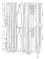
図3は、図2に示すカラムAD変換要素AとカラムAD変換要素Bとのタイミングチャートを示している。図3に示すタイミングチャートにおいては、画素アレイ1の第i(i=1〜8)行目の画素信号を読み出す水平走査期間T1と、第i+1行目の画素信号を読み出す水平走査期間T2とを示し、水平走査期間T1では、カラムAD変換要素Aが第i行目の画素信号を画素アレイ1から読み出し、水平走査期間T2では、カラムAD変換要素Bが第i+1行目の画素信号を画素アレイ1から読み出しているものとする。なお、n=8の場合、第i+1行目は第1行目を示す。
FIG. 3 shows a timing chart of the column AD conversion element A and the column AD conversion element B shown in FIG. In the timing chart shown in FIG. 3, a horizontal scanning period T1 for reading out pixel signals in the i-th (i = 1 to 8) rows of the
水平走査期間T1は、期間T11と期間T12とに分けられる。期間T11においては、第i行目の画素信号を画素アレイ1から読み出す処理(1)が実行される。
The horizontal scanning period T1 is divided into a period T11 and a period T12. In the period T11, a process (1) for reading out the pixel signal of the i-th row from the
具体的には、φCOL_A=H(ハイレベル)により、スイッチSW12Aがオンされ、垂直信号線VL1とGCA部10Aとが接続され、画素アレイ1からノイズ信号、画素信号が順次読み出され、GCA部10AによりCDS処理が行われ、画素信号からノイズ信号が除去される。
Specifically, by φCOL_A = H (high level), the switch SW12A is turned on, the vertical signal line VL1 and the
また、φPRST_A=H・Lにより、スイッチSW11Aがオン・オフされ、コンデンサC2Aがリセットされる。また、φS1_A=H・L,φS2_A=H・Lにより、スイッチSW23A,SW24Aがオン・オフされ、コンパレータ部20Aがリセットされる。
Further, by φPRST_A = H · L, the switch SW11A is turned on / off, and the capacitor C2A is reset. Further, by φS1_A = H · L and φS2_A = H · L, the switches SW23A and SW24A are turned on / off, and the
期間T12においては、第i行目の画素信号の上位ブロックをAD変換する処理(2)と、第i−1行目の画素信号の下位ブロックをAD変換する処理(3)とがオーバーラップして実行される。なお、n=1の場合、第i−1行目は第8行目を示す。以下の説明では、カラムAD変換要素Aが処理(2)を実行し、カラムAD変換要素Bが処理(3)を実行しているものとする。 In the period T12, the process (2) for AD conversion of the upper block of the pixel signal in the i-th row overlaps the process (3) for AD conversion of the lower block of the pixel signal in the i-1th row. Executed. When n = 1, the (i−1) -th line indicates the eighth line. In the following description, it is assumed that the column AD conversion element A executes the process (2) and the column AD conversion element B executes the process (3).
期間T12においては、まず、φSH_A=L(ローレベル)により、スイッチSW21Aがオフされ、コンデンサC3Aによりノイズ信号の除去された画素信号がサンプルホールドされる。このとき、制御部5は、Ramp1の出力を開始する。また、このとき、COMPOUT1_A=Hであるため、スイッチSW22Aがオンされており、Ramp1は、スイッチSW22Aを介してコンパレータ21Aに入力される。また、このとき、カウンタ71はカウント動作を開始する。
In the period T12, first, the switch SW21A is turned off by φSH_A = L (low level), and the pixel signal from which the noise signal is removed is sampled and held by the capacitor C3A. At this time, the control unit 5 starts outputting Ramp1. At this time, since COMPOUT1_A = H, the switch SW22A is turned on, and Ramp1 is input to the
そして、コンパレータ21Aにより画素信号とRamp1とのレベルが比較され、Ramp1のレベルが画素信号のレベルを下回ると(タイミングTM1)、コンパレータ21Aは出力信号を反転させる。コンパレータ21Aからにより反転された出力信号は、コンデンサC6A、コンパレータ22Aを介してロジック回路30Aに入力される。これにより、COMPOUT_1=Lとなり、ラッチ回路41−1によりカウンタ71の現在のカウント値「10」がラッチされ、かつ、スイッチSW22Aがオフされる。
Then, the level of the pixel signal and Ramp1 is compared by the
また、期間T12において、φSH_A=Lにされると、制御部5は、Ramp2の出力を開始する。そして、コンパレータ21BによりRamp2とコンデンサC3Bにより保持された画素信号とが比較され、Ramp2のレベルが画素信号のレベルを上回ると(タイミングTM2)、コンパレータ21Bは、出力信号を反転させる。これにより、COMPOUT2_B=Lとなり、ラッチ回路42−2により、カウンタ72の現在のカウント値「01」がラッチされる。なお、カウンタ72が「00」ではなく「11」からカウント動作を開始しているのは、Ramp2のレベルが経時的に増大するからである。
Further, when φSH_A = L is set in the period T12, the control unit 5 starts outputting Ramp2. The
また、水平走査期間T1においては、φRD_A=Hとされ、スイッチ51−1,51−2がオンされている。これにより、ラッチ回路41−1,41−2にラッチされた第i−2行目のデジタルデータを水平信号線L1に出力する処理(4)が処理(1)〜(3)とオーバーラップして実行される。 In the horizontal scanning period T1, φRD_A = H is set, and the switches 51-1 and 51-2 are turned on. Thereby, the process (4) for outputting the digital data of the (i-2) th row latched by the latch circuits 41-1 and 41-2 to the horizontal signal line L1 overlaps the processes (1) to (3). Executed.
水平走査期間T2は、期間T21と期間T22とに分けられる。期間T21では、第i+1行目の画素信号を画素アレイ1から読み出す処理(1)が実行される。また、期間T22では、第i+1行目の画素信号の上位ブロックをAD変換する処理(2)と、第i行目の画素信号の下位ブロックをAD変換する処理(3)とが実行される。また、水平走査期間T2においては、第i−1行目のデジタルデータをラッチ回路42−1,42−2から出力する処理(4)が、処理(1)〜(3)とオーバーラップして実行される。
The horizontal scanning period T2 is divided into a period T21 and a period T22. In the period T21, a process (1) for reading out the pixel signal of the (i + 1) th row from the
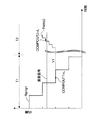
図4は、コンパレータ部20Aの処理を説明するグラフである。図4において、縦軸は電圧を示し、横軸は時間を示している。
FIG. 4 is a graph illustrating the processing of the
水平走査期間T1において、φSH_A=Lとなると、コンパレータ21Aは、Ramp1が入力される。そして、Ramp1のレベルが、コンデンサC3Aにより保持された画素信号のレベルを下回ると、コンパレータ21Aは出力信号を反転させる。これにより、COMPOUT1=Lとなり、ラッチ回路41−1にカウンタ71によるカウント値がラッチされる。このとき、コンパレータ21Aの出力信号が反転したときのRamp1の電圧V1がコンデンサC5Aに保持される。以上により第i行目の画素信号の上位ブロックのAD変換が終了する。
When φSH_A = L in the horizontal scanning period T1, Ramp1 is input to the
水平走査期間T2において、φSH_A=Lになると、コンパレータ21Aは、Ramp2が入力される。そして、Ramp2のレベルがコンデンサC3Aに保持された画素信号のレベルを上回ると、コンパレータ21Aは出力信号を反転させる。この場合、コンデンサC5Aに電圧V1が保持されているため、Ramp2の初期の電圧はV1となる。また、コンデンサC4A,C5Aの容量比によって、Ramp2の1段の電圧値がRamp1の1段の電圧値の1/4とされる。そのため、Ramp2を用いることで、少ないクロック数でありながら、画素信号を高い分解能によりAD変換することができる。
When φSH_A = L in the horizontal scanning period T2, Ramp2 is input to the
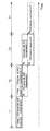
図5は、図2に示すカラムAD変換部3のシーケンス図を示している。なお、図3のシーケンス図では、第i行目と第i+1行目の2行分の画素信号に対する処理が示されている。まず、水平走査期間T1において、処理(1)が実行され、カラムAD変換要素Aにより第i行目の画素信号が読み出される。また、水平走査期間T1において、処理(1)に引き続いて、処理(2)が実行され、カラムAD変換要素Aにより第i行目の画素信号の上位ブロックがAD変換される。
FIG. 5 shows a sequence diagram of the
次に、水平走査期間T2において、カラムAD変換要素Aにより第i行目の画素信号の下位ブロックがAD変換される。ここで、水平走査期間T2においては、処理(3)とオーバーラップして処理(1)、(2)が実行され、カラムAD変換要素Bにより第i+1行目の画素信号が読み出され、読み出された第i+1行目の画素信号の上位ブロックがカラムAD変換要素BによりAD変換される。 Next, in the horizontal scanning period T2, the column AD conversion element A performs AD conversion on the lower block of the pixel signal in the i-th row. Here, in the horizontal scanning period T2, the processing (1) and (2) are executed so as to overlap with the processing (3), and the pixel signal of the (i + 1) -th row is read by the column AD conversion element B and read. The upper block of the pixel signal in the (i + 1) th row thus output is AD converted by the column AD conversion element B.
次に、水平走査期間T3において、カラムAD変換要素Aにより、第i行目のデジタルデータがラッチ回路41−1、41−2から出力される処理(4)が実行される。また、水平走査期間T3において、カラムAD変換要素Bにより、処理(4)とオーバーラップして第i+1行目の画素信号の下位ブロックをAD変換する処理(3)が実行される。 Next, in the horizontal scanning period T3, the column AD conversion element A performs processing (4) in which the i-th row digital data is output from the latch circuits 41-1 and 41-2. Further, in the horizontal scanning period T3, the column AD conversion element B executes a process (3) for performing A / D conversion on the lower block of the pixel signal on the (i + 1) th row, overlapping with the process (4).
次に、水平走査期間T4において、カラムAD変換要素Bにより、処理(4)が実行され、第i+1行目のデジタルデータがラッチ回路42−1,42−2から出力される。 Next, in the horizontal scanning period T4, the process (4) is executed by the column AD conversion element B, and the digital data of the (i + 1) th row is output from the latch circuits 42-1 and 42-2.
このように、本固体撮像装置によれば、制御部5は、カラムAD変換要素A,Bに、それぞれ異なる行の画素信号の異なるブロックのAD変換をオーバーラップして実行させる。このとき、制御部5は、ある1水平走査期間において、カラムAD変換要素j(j=A,B)に第i行目の画素信号を読み出させた後、第i行目の画素信号の上位ブロックをAD変換させる。 As described above, according to the present solid-state imaging device, the control unit 5 causes the column AD conversion elements A and B to execute AD conversion of different blocks of pixel signals in different rows in an overlapping manner. At this time, the control unit 5 causes the column AD conversion element j (j = A, B) to read out the pixel signal of the i-th row and then the pixel signal of the i-th row in one horizontal scanning period. AD conversion is performed on the upper block.
したがって、1水平走査期間において、第i行目の画素信号を読み取る処理(1)と、第i行目の画素信号の上位ブロックをAD変換する処理(2)との2つの処理のみが行われ、従来のように画素信号を読み出す処理と、読み出した画素信号の上位ブロックをAD変換する処理と、読み出した画素信号の下位ブロックをAD変換する処理とが同時に実行されないため、上位ブロックの画素信号のAD変換処理の期間を一定時間以上確保することが可能となり、上位ブロックの画素信号を高精度にAD変換することができ、かつ、1水平走査期間を短縮化することができる。 Therefore, in one horizontal scanning period, only two processes of the process (1) for reading the pixel signal in the i-th row and the process (2) for AD-converting the upper block of the pixel signal in the i-th row are performed. Since the processing for reading out the pixel signal, the processing for AD conversion of the upper block of the read pixel signal, and the processing for AD conversion of the lower block of the read pixel signal are not performed at the same time, the pixel signal of the upper block The AD conversion processing period can be ensured for a certain time or more, the pixel signals of the upper block can be AD-converted with high accuracy, and one horizontal scanning period can be shortened.
(実施の形態2)
次に、本発明の実施の形態2による固体撮像装置について説明する。実施の形態2による固体撮像装置は、カラムAD変換要素A,Bにラッチ回路41−1,41−2と、GCA部10Aとを共用させることを特徴とする。なお、本実施の形態において、実施の形態1と同一のものは同一の符号を用いて説明を省略する。
(Embodiment 2)
Next, a solid-state imaging device according to
図6は、実施の形態2によるカラムAD変換部3の回路図を示している。GCA部10Aは、出力側がコンパレータ部20Aに接続されると共にコンパレータ部20Bに接続され、カラムAD変換要素A,Bに共用されている。
FIG. 6 shows a circuit diagram of the column
また、ラッチ部40Aは、スイッチ部80Aを介してロジック回路30Aの出力側とロジック回路30Bの出力側とに接続され、カラムAD変換要素A,Bに共用されている。
The
本実施の形態においては、図2に示すGCA部10Bが省かれたため、GCA部10Aと垂直信号線VL1との間のスイッチSW12Aが省かれている。また、ラッチ部40Bが省かれたため、ラッチ部40Bを選択するためのスイッチ52−1,52−2,62−1,62−2が省かれている。また、ロジック回路30A,30Bとラッチ部40Aとの間には、ロジック回路30Aとロジック回路30Bとを選択するためのスイッチ81,82が接続されている。
In the present embodiment, since the
スイッチ81は、R−Sフリップフロップ33AとR−Sフリップフロップ33Bとを選択する。スイッチ82は、R−Sフリップフロップ34AとR−Sフリップフロップ34Bとを選択する。よって、ラッチ回路41−1は、カラムAD変換要素A又はカラムAD変換要素BでAD変換される上位ブロックのデジタルデータをラッチし、ラッチ回路41−2は、カラムAD変換要素A又はカラムAD変換要素BでAD変換される下位ブロックのデジタルデータをラッチする。
The
図7は、図6に示すカラムAD変換部3のタイミングチャートを示している。水平走査期間T1において、φSH_A=Lにより第i行目の画素信号がコンデンサC3Aによりサンプルホールドされる。
FIG. 7 shows a timing chart of the
また、水平走査期間T1においては、φSEL_A=Hとされている。そのため、スイッチ81にはCOMPOUT1_Aが入力され、COMPOUT1_A=Lとなると(タイミングTM1)、ラッチ回路41−1はカウンタ71の現在のカウント値をラッチする。
In the horizontal scanning period T1, φSEL_A = H. Therefore, COMPOUT1_A is input to the
また、水平走査期間T1においては、φSEL_B=Lとされている。そのため、スイッチ82には、COMPOUT2_Bが入力され、COMPOUT2_B=Lとなると(タイミングTM2)、ラッチ回路41−2はカウンタ72の現在のカウント値をラッチする。
In the horizontal scanning period T1, φSEL_B = L. Therefore, COMPOUT2_B is input to the
以上により、第i行目の画素信号の上位ブロックをAD変換する処理(2)と、第i−1行目の画素信号の下位ブロックをAD変換する処理(3)とがオーバーラップして実行される。 As described above, the process (2) for AD-converting the upper block of the pixel signal in the i-th row and the process (3) for AD-converting the lower block of the pixel signal in the (i-1) -th row are executed in an overlapping manner. Is done.
また、水平走査期間T2において、φSH_B=Lにより第i+1行目の画素信号がコンデンサC3Bによりサンプルホールドされる。 In the horizontal scanning period T2, the pixel signal in the (i + 1) th row is sampled and held by the capacitor C3B due to φSH_B = L.
水平走査期間T2においては、φSEL_B=Hとされている。そのため、スイッチ82にはCOMPOUT2_Aが入力され、COMPOUT2_A=Lとなると(タイミングTM3)、ラッチ回路41−2はカウンタ72の現在のカウント値をラッチする。
In the horizontal scanning period T2, φSEL_B = H. Therefore, COMPOUT2_A is input to the
また、水平走査期間T2においては、φSEL_A=Lとされている。そのため、スイッチ81には、COMPOUT1_Bが入力され、COMPOUT1_B=Lとなると(タイミングTM4)、ラッチ回路41−1はカウンタ71の現在のカウント値をラッチする。
In the horizontal scanning period T2, φSEL_A = L. Therefore, COMPOUT1_B is input to the
以上により、第i+1行目の画素信号の上位ブロックをAD変換する処理(2)と、第i行目の画素信号の下位ブロックをAD変換する処理(3)とがオーバーラップして実行される。 As described above, the process (2) for AD-converting the upper block of the pixel signal in the i + 1-th row and the process (3) for AD-converting the lower block of the pixel signal in the i-th row are executed in an overlapping manner. .
実施の形態2の固体撮像装置では、ラッチ部40Aを共有させているため、ラッチ回路41−1とラッチ回路41−2とは、第i行目のデジタルデータの上位ブロックと下位ブロックとを同時にラッチすることができない。すなわち、第i行目のデジタルデータの下位ブロックは、第i行目のデジタルデータの上位ブロックに対して1水平走査期間だけ遅延して出力される。したがって、画像処理部6は、第i行目のデジタルデータの上位ブロックを保持して1水平走査期間遅延させ、第i行目のデジタルデータの下位ブロックと同期させる。
In the solid-state imaging device of the second embodiment, since the
このように、実施の形態2の固体撮像装置によれば、GCA部10A及びラッチ部40AがカラムAD変換要素A,Bにより共用されるため、回路規模の縮小を図ることができる。
Thus, according to the solid-state imaging device of the second embodiment, since the
なお、実施の形態1,2においては、上位ブロックを2ビット、下位ブロックを2ビットとしたが、本発明はこれに限定されず、例えば上位ブロックを4ビット、下位ブロックを10ビットというようにして、他のビットを採用してもよい。 In the first and second embodiments, the upper block is 2 bits and the lower block is 2 bits. However, the present invention is not limited to this. For example, the upper block is 4 bits and the lower block is 10 bits. Other bits may be employed.
また、実施の形態1,2においては、画素信号を上位ブロックと下位ブロックとの2つのブロックに分けたが、これに限定されず、3個以上の第1〜第nのブロックに分けても良い。 In the first and second embodiments, the pixel signal is divided into two blocks, an upper block and a lower block. However, the present invention is not limited to this, and the pixel signal may be divided into three or more first to nth blocks. good.
図8は、画素信号を第1〜第nのブロックに分けた場合のシーケンス図を示している。図8において、かぎ括弧内の数値は行番号を示し、かぎ括弧の下付で示す丸括弧内の数値はブロック番号を示し、丸印内の数値はカラムAD変換要素の要素番号を示している。 FIG. 8 shows a sequence diagram when the pixel signal is divided into first to nth blocks. In FIG. 8, the numerical value in the brackets indicates the line number, the numerical value in the parentheses indicated by the parentheses indicates the block number, and the numerical value in the circle indicates the element number of the column AD conversion element. .
この場合、以下の構成を採用する。カラムAD変換部3を第1〜第nのカラムAD変換要素により構成する。また、第1〜第nのカラムAD変換要素は、画素アレイ1から読み出した画素信号を最上位ビットから最下位ビットに向けて第1〜第nのブロックに分け、各ブロックを1水平走査期間単位で順次にAD変換する。
In this case, the following configuration is adopted. The column
そして、図8に示すように、ある1水平走査期間において、制御部5は、第jのカラムAD変換要素に、第i行目の読み出させた後、第i行目の第1のブロックの画素信号をAD変換させる処理と、第k(k=j+1〜n)のカラムAD変換要素に第(i−(k−j))行目の第(k−j+1)ブロックの画素信号をAD変換させ、かつ、第k(k=1〜j−1)のカラムAD変換要素に第(i−(n+k−j))行目の第(n+k−j+1)のブロックの画素信号をAD変換させる処理と、第jのカラムAD変換要素に第i−n行目のデジタルデータ出力させる処理とをオーバーラップして実行させればよい。 Then, as shown in FIG. 8, in one horizontal scanning period, the control unit 5 causes the j-th column AD conversion element to read the i-th row and then the first block on the i-th row. And AD conversion of the pixel signal of the (k−j + 1) th row in the (i− (k−j)) th row to the kth (k = j + 1 to n) column AD conversion elements. The pixel signal of the (n + k−j + 1) th block in the (i− (n + k−j)) th row is AD converted to the kth (k = 1 to j−1) column AD conversion element. The processing and the processing for outputting the digital data in the ith row to the jth column AD conversion element may be executed in an overlapping manner.
実施の形態1,2では、カラムAD変換部3を2回積分型のAD変換回路により構成したが、本発明はこれに限定されず、他のAD変換回路を採用してもよい。この場合、上位ブロックを逐次比較型のAD変換回路によりAD変換させ、下位ブロックを積分型のAD変換回路を採用することが好ましい。
In the first and second embodiments, the column
1 画素アレイ
2 垂直走査回路
3 カラムAD変換部
4 水平走査回路
5 制御部
7 画像処理部
8 画像メモリ
10A,10B GCA部
20A,20B コンパレータ部
30A,30B ロジック回路
40A,40B ラッチ部
50A,50B スイッチ部
80A スイッチ部
DESCRIPTION OF
Claims (7)
所定行×所定列のマトリックス状に配列された複数の画素から構成される画素アレイと、
前記画素アレイの各行をサイクリックに選択する垂直走査回路と、
前記画素アレイの各列に対応して設けられ、前記垂直走査回路により選択された行の画素信号を読み出し、AD変換するカラムAD変換部と、
制御部とを備え、
各列のカラムAD変換部は、第1〜第n(nは2以上の整数)のカラムAD変換要素を備え、
前記第1〜第nのカラムAD変換要素は、前記画素アレイから読み出した画素信号を最上位ビットから最下位ビットに向けて第1〜第nのブロックに分け、各ブロックを1水平走査期間単位で順次にAD変換し、
前記制御部は、前記第1〜第nのカラムAD変換要素に、それぞれ異なる行の画素信号の異なるブロックのAD変換をオーバーラップして実行させ、ある1水平走査期間において、第j(j=1〜n)のカラムAD変換要素に第i行目の画素信号を読み出させた後、前記第i行目の画素信号の第1のブロックをAD変換させることを特徴とする固体撮像装置。 A column parallel AD conversion type solid-state imaging device,
A pixel array composed of a plurality of pixels arranged in a matrix of predetermined rows x predetermined columns;
A vertical scanning circuit that cyclically selects each row of the pixel array;
A column AD conversion unit that is provided corresponding to each column of the pixel array, reads a pixel signal of a row selected by the vertical scanning circuit, and performs AD conversion;
A control unit,
The column AD conversion unit of each row includes first to n-th (n is an integer of 2 or more) column AD conversion elements,
The first to nth column AD conversion elements divide a pixel signal read from the pixel array into first to nth blocks from the most significant bit to the least significant bit, and each block is in units of one horizontal scanning period. AD conversion in order,
The control unit causes the first to nth column AD conversion elements to perform AD conversion of different blocks of pixel signals in different rows in an overlapping manner, and in a certain horizontal scanning period, the jth (j = j = 1 to n), after the column AD conversion element of the i-th row reads out the pixel signal of the i-th row, the first block of the pixel signal of the i-th row is AD-converted.
AD変換されたデジタルデータをラッチするラッチ部と、
前記ラッチ部によりラッチされたデジタルデータを伝送する水平信号線と前記ラッチ部との間に接続されたスイッチ部とを備え、
前記ラッチ部は、前記第1〜第nのブロックのデジタルデータをラッチするn個のラッチ回路を備え、
前記スイッチ部は、前記第1〜第nのブロックに対応するスイッチを備えることを特徴とする請求項3記載の固体撮像装置。 The first to nth column AD conversion elements are:
A latch unit for latching the AD converted digital data;
A horizontal signal line for transmitting digital data latched by the latch unit and a switch unit connected between the latch unit;
The latch unit includes n latch circuits for latching digital data of the first to nth blocks,
The solid-state imaging device according to claim 3, wherein the switch unit includes switches corresponding to the first to n-th blocks.
前記ラッチ部は、前記第1〜第nのブロックのデジタルデータをラッチし、前記第1〜第nのカラムAD変換要素に共用されるn個のラッチ回路を備えることを特徴とする請求項3記載の固体撮像装置。 The first to n-th column AD conversion elements include a latch unit that latches AD-converted pixel signals,
The latch unit includes n latch circuits that latch digital data of the first to n-th blocks and are shared by the first to n-th column AD conversion elements. The solid-state imaging device described.
前記ラッチ部の前段に設けられたコンパレータと、
各カラムAD変換要素のコンパレータのうちいずれか1つのコンパレータと、n個のラッチ回路のうちいずれか1つのラッチ回路とを接続するスイッチ部とを備えることを特徴とする請求項5記載の固体撮像装置。 Each column AD conversion element is
A comparator provided in a preceding stage of the latch unit;
6. The solid-state imaging according to claim 5, further comprising a switch unit that connects any one of the comparators of the column AD conversion elements and any one of the n latch circuits. apparatus.
Priority Applications (2)
| Application Number | Priority Date | Filing Date | Title |
|---|---|---|---|
| JP2008163007A JP5077091B2 (en) | 2008-06-23 | 2008-06-23 | Solid-state imaging device |
| US12/486,871 US8072527B2 (en) | 2008-06-23 | 2009-06-18 | Solid state image sensing device |
Applications Claiming Priority (1)
| Application Number | Priority Date | Filing Date | Title |
|---|---|---|---|
| JP2008163007A JP5077091B2 (en) | 2008-06-23 | 2008-06-23 | Solid-state imaging device |
Publications (2)
| Publication Number | Publication Date |
|---|---|
| JP2010004440A true JP2010004440A (en) | 2010-01-07 |
| JP5077091B2 JP5077091B2 (en) | 2012-11-21 |
Family
ID=41430841
Family Applications (1)
| Application Number | Title | Priority Date | Filing Date |
|---|---|---|---|
| JP2008163007A Expired - Fee Related JP5077091B2 (en) | 2008-06-23 | 2008-06-23 | Solid-state imaging device |
Country Status (2)
| Country | Link |
|---|---|
| US (1) | US8072527B2 (en) |
| JP (1) | JP5077091B2 (en) |
Families Citing this family (10)
| Publication number | Priority date | Publication date | Assignee | Title |
|---|---|---|---|---|
| JP5094498B2 (en) * | 2008-03-27 | 2012-12-12 | キヤノン株式会社 | Solid-state imaging device and imaging system |
| JP5332041B2 (en) | 2009-03-13 | 2013-11-06 | ルネサスエレクトロニクス株式会社 | Solid-state imaging device |
| JP5762199B2 (en) | 2011-07-28 | 2015-08-12 | キヤノン株式会社 | Solid-state imaging device |
| JP2013090305A (en) * | 2011-10-21 | 2013-05-13 | Sony Corp | Comparator, ad converter, solid state image pickup device and camera system |
| US9843756B2 (en) | 2015-05-27 | 2017-12-12 | Samsung Electronics Co., Ltd. | Imaging devices, arrays of pixels receiving photocharges in bulk of select transistor, and methods |
| JP6727771B2 (en) * | 2015-08-13 | 2020-07-22 | キヤノン株式会社 | Imaging device |
| KR101679598B1 (en) * | 2016-01-04 | 2016-11-25 | 주식회사 동부하이텍 | Image sensor |
| CN110771157B (en) * | 2017-03-31 | 2022-02-08 | 普里露尼库斯新加坡私人有限公司 | Solid-state imaging device, method for driving solid-state imaging device, and electronic apparatus |
| KR20190020408A (en) * | 2017-08-21 | 2019-03-04 | 에스케이하이닉스 주식회사 | Two-step single-slope comparator with high linearity and cmos image sensor thereof |
| JP6929750B2 (en) * | 2017-09-29 | 2021-09-01 | キヤノン株式会社 | Imaging device, imaging system, moving object |
Citations (9)
| Publication number | Priority date | Publication date | Assignee | Title |
|---|---|---|---|---|
| JPH0548460A (en) * | 1991-06-05 | 1993-02-26 | Matsushita Electric Ind Co Ltd | A/d converter and sensor using the same and three-dimensional integrated circuit |
| JP2002027331A (en) * | 2000-07-03 | 2002-01-25 | Canon Inc | Signal processing device, image pickup device and image pickup system |
| JP2002232291A (en) * | 2001-02-02 | 2002-08-16 | Riniaseru Design:Kk | Analog/digital converter and image sensor provided with the same |
| JP2005347932A (en) * | 2004-06-01 | 2005-12-15 | Canon Inc | Solid-state imaging unit and imaging system |
| JP2007060401A (en) * | 2005-08-25 | 2007-03-08 | Matsushita Electric Ind Co Ltd | Analog front end for image sensor |
| JP2007336374A (en) * | 2006-06-16 | 2007-12-27 | Canon Inc | Imaging device and its processing method |
| JP2008141610A (en) * | 2006-12-04 | 2008-06-19 | Matsushita Electric Ind Co Ltd | Solid-state imaging apparatus, and imaging system |
| JP2008167004A (en) * | 2006-12-27 | 2008-07-17 | Sony Corp | Solid state imaging apparatus, method for driving the same, and imaging apparatus |
| JP2008236462A (en) * | 2007-03-22 | 2008-10-02 | Seiko Epson Corp | Ad conversion apparatus for solid-state image pickup element |
Family Cites Families (6)
| Publication number | Priority date | Publication date | Assignee | Title |
|---|---|---|---|---|
| US4954897A (en) * | 1987-05-22 | 1990-09-04 | Nikon Corporation | Electronic still camera system with automatic gain control of image signal amplifier before image signal recording |
| US6873364B1 (en) * | 2000-06-08 | 2005-03-29 | Micron Technology, Inc. | Low-power signal chain for image sensors |
| US7129883B2 (en) * | 2004-02-23 | 2006-10-31 | Sony Corporation | Method and apparatus for AD conversion, semiconductor device for detecting distribution of physical quantity, and electronic apparatus |
| JP2006197393A (en) * | 2005-01-14 | 2006-07-27 | Canon Inc | Solid-state imaging device, driving method thereof and camera |
| US20060187329A1 (en) * | 2005-02-24 | 2006-08-24 | Micron Technology, Inc. | Clamped capacitor readout noise rejection circuit for imagers |
| US7825975B2 (en) * | 2008-02-25 | 2010-11-02 | Fairchild Imaging, Inc. | Imaging array with improved dynamic range |
-
2008
- 2008-06-23 JP JP2008163007A patent/JP5077091B2/en not_active Expired - Fee Related
-
2009
- 2009-06-18 US US12/486,871 patent/US8072527B2/en not_active Expired - Fee Related
Patent Citations (9)
| Publication number | Priority date | Publication date | Assignee | Title |
|---|---|---|---|---|
| JPH0548460A (en) * | 1991-06-05 | 1993-02-26 | Matsushita Electric Ind Co Ltd | A/d converter and sensor using the same and three-dimensional integrated circuit |
| JP2002027331A (en) * | 2000-07-03 | 2002-01-25 | Canon Inc | Signal processing device, image pickup device and image pickup system |
| JP2002232291A (en) * | 2001-02-02 | 2002-08-16 | Riniaseru Design:Kk | Analog/digital converter and image sensor provided with the same |
| JP2005347932A (en) * | 2004-06-01 | 2005-12-15 | Canon Inc | Solid-state imaging unit and imaging system |
| JP2007060401A (en) * | 2005-08-25 | 2007-03-08 | Matsushita Electric Ind Co Ltd | Analog front end for image sensor |
| JP2007336374A (en) * | 2006-06-16 | 2007-12-27 | Canon Inc | Imaging device and its processing method |
| JP2008141610A (en) * | 2006-12-04 | 2008-06-19 | Matsushita Electric Ind Co Ltd | Solid-state imaging apparatus, and imaging system |
| JP2008167004A (en) * | 2006-12-27 | 2008-07-17 | Sony Corp | Solid state imaging apparatus, method for driving the same, and imaging apparatus |
| JP2008236462A (en) * | 2007-03-22 | 2008-10-02 | Seiko Epson Corp | Ad conversion apparatus for solid-state image pickup element |
Also Published As
| Publication number | Publication date |
|---|---|
| US8072527B2 (en) | 2011-12-06 |
| US20090316034A1 (en) | 2009-12-24 |
| JP5077091B2 (en) | 2012-11-21 |
Similar Documents
| Publication | Publication Date | Title |
|---|---|---|
| JP5077091B2 (en) | Solid-state imaging device | |
| EP1655840B1 (en) | Analog-to-digital conversion method, analog-to-digital converter, semiconductor device for detecting distribution of physical quantity, and electronic apparatus | |
| US9450596B2 (en) | Ramp and successive approximation register analog to digital conversion methods, systems and apparatus | |
| US7518539B2 (en) | Concurrent correlated double sampling and analog-to-digital conversion | |
| TWI578711B (en) | Method and system for implementing correlated multi-sampling with improved analog-to-digital converter linearity | |
| US8665354B2 (en) | Solid-state image pickup device | |
| JP2010063055A (en) | Successive approximation type a/d converter, successive approximation type a/d converter controlling method, solid-state imaging device, and image capturing apparatus | |
| JP2011526088A (en) | Imaging array with improved dynamic range | |
| KR20190020408A (en) | Two-step single-slope comparator with high linearity and cmos image sensor thereof | |
| US10715757B2 (en) | A/D converter | |
| US20120242877A1 (en) | Solid-state imaging apparatus | |
| US10498992B2 (en) | Single-slope comparison device with low-noise, and analog-to-digital conversion device and CMOS image sensor including the same | |
| KR20160145217A (en) | Counting circuit, image sensing device with the counting circuit and read-out method of the mage sensing device | |
| JP4423111B2 (en) | Imaging device and imaging system | |
| JP5749579B2 (en) | AD conversion circuit and solid-state imaging device | |
| US9160318B2 (en) | Data processing circuit and solid-state imaging device | |
| JP2010004439A (en) | Solid-state image pickup device | |
| JP4478798B2 (en) | Cyclic A / D converter with offset reduction function and method for reducing offset voltage | |
| US20100188542A1 (en) | Imaging device and image sensor chip | |
| KR101738694B1 (en) | Parallel mode readout ic for x-ray image sensor and method thereof | |
| JP6903154B2 (en) | Amplifier circuit and analog-to-digital conversion system equipped with it | |
| JP2011055535A (en) | Sequential comparison type a/d converter and imaging device | |
| JP2014120987A (en) | A/d conversion circuit and solid-state imaging device | |
| JP3576073B2 (en) | Solid-state imaging device | |
| JP7198835B2 (en) | AD conversion device, imaging device, endoscope system, and AD conversion method |
Legal Events
| Date | Code | Title | Description |
|---|---|---|---|
| A621 | Written request for application examination |
Free format text: JAPANESE INTERMEDIATE CODE: A621 Effective date: 20110215 |
|
| A977 | Report on retrieval |
Free format text: JAPANESE INTERMEDIATE CODE: A971007 Effective date: 20120724 |
|
| TRDD | Decision of grant or rejection written | ||
| A01 | Written decision to grant a patent or to grant a registration (utility model) |
Free format text: JAPANESE INTERMEDIATE CODE: A01 Effective date: 20120731 |
|
| A01 | Written decision to grant a patent or to grant a registration (utility model) |
Free format text: JAPANESE INTERMEDIATE CODE: A01 |
|
| A61 | First payment of annual fees (during grant procedure) |
Free format text: JAPANESE INTERMEDIATE CODE: A61 Effective date: 20120813 |
|
| FPAY | Renewal fee payment (event date is renewal date of database) |
Free format text: PAYMENT UNTIL: 20150907 Year of fee payment: 3 |
|
| R150 | Certificate of patent or registration of utility model |
Free format text: JAPANESE INTERMEDIATE CODE: R150 |
|
| S111 | Request for change of ownership or part of ownership |
Free format text: JAPANESE INTERMEDIATE CODE: R313111 |
|
| R350 | Written notification of registration of transfer |
Free format text: JAPANESE INTERMEDIATE CODE: R350 |
|
| LAPS | Cancellation because of no payment of annual fees |