JP2010003901A - Photoelectric converting element and solid-state imaging element - Google Patents
Photoelectric converting element and solid-state imaging element Download PDFInfo
- Publication number
- JP2010003901A JP2010003901A JP2008161770A JP2008161770A JP2010003901A JP 2010003901 A JP2010003901 A JP 2010003901A JP 2008161770 A JP2008161770 A JP 2008161770A JP 2008161770 A JP2008161770 A JP 2008161770A JP 2010003901 A JP2010003901 A JP 2010003901A
- Authority
- JP
- Japan
- Prior art keywords
- photoelectric conversion
- layer
- conversion element
- region
- light
- Prior art date
- Legal status (The legal status is an assumption and is not a legal conclusion. Google has not performed a legal analysis and makes no representation as to the accuracy of the status listed.)
- Granted
Links
- 238000003384 imaging method Methods 0.000 title claims abstract description 25
- 239000013078 crystal Substances 0.000 claims abstract description 29
- 238000006243 chemical reaction Methods 0.000 claims description 226
- 239000000758 substrate Substances 0.000 claims description 86
- 230000000903 blocking effect Effects 0.000 claims description 77
- 239000004065 semiconductor Substances 0.000 claims description 26
- 238000002347 injection Methods 0.000 claims description 7
- 239000007924 injection Substances 0.000 claims description 7
- 239000003086 colorant Substances 0.000 claims description 5
- 238000003860 storage Methods 0.000 claims description 4
- 238000009825 accumulation Methods 0.000 claims description 3
- 238000010030 laminating Methods 0.000 claims description 3
- 230000002542 deteriorative effect Effects 0.000 abstract 1
- 239000010410 layer Substances 0.000 description 253
- 239000010408 film Substances 0.000 description 49
- XUIMIQQOPSSXEZ-UHFFFAOYSA-N Silicon Chemical compound [Si] XUIMIQQOPSSXEZ-UHFFFAOYSA-N 0.000 description 42
- 229910052710 silicon Inorganic materials 0.000 description 42
- 239000010703 silicon Substances 0.000 description 42
- 239000000975 dye Substances 0.000 description 35
- 239000003446 ligand Substances 0.000 description 29
- 239000000463 material Substances 0.000 description 24
- 125000004432 carbon atom Chemical group C* 0.000 description 21
- -1 hydrazone compounds Chemical class 0.000 description 19
- 150000002894 organic compounds Chemical class 0.000 description 18
- 239000011368 organic material Substances 0.000 description 15
- 238000007740 vapor deposition Methods 0.000 description 15
- 229910000480 nickel oxide Inorganic materials 0.000 description 12
- 150000001875 compounds Chemical class 0.000 description 11
- 238000000151 deposition Methods 0.000 description 10
- 230000008021 deposition Effects 0.000 description 10
- KFZMGEQAYNKOFK-UHFFFAOYSA-N Isopropanol Chemical compound CC(C)O KFZMGEQAYNKOFK-UHFFFAOYSA-N 0.000 description 9
- DZVCFNFOPIZQKX-LTHRDKTGSA-M merocyanine Chemical class [Na+].O=C1N(CCCC)C(=O)N(CCCC)C(=O)C1=C\C=C\C=C/1N(CCCS([O-])(=O)=O)C2=CC=CC=C2O\1 DZVCFNFOPIZQKX-LTHRDKTGSA-M 0.000 description 7
- 229910052782 aluminium Inorganic materials 0.000 description 6
- 238000010586 diagram Methods 0.000 description 6
- GVEPBJHOBDJJJI-UHFFFAOYSA-N fluoranthene Chemical class C1=CC(C2=CC=CC=C22)=C3C2=CC=CC3=C1 GVEPBJHOBDJJJI-UHFFFAOYSA-N 0.000 description 6
- 238000010438 heat treatment Methods 0.000 description 6
- RAXXELZNTBOGNW-UHFFFAOYSA-N imidazole Natural products C1=CNC=N1 RAXXELZNTBOGNW-UHFFFAOYSA-N 0.000 description 6
- WFKWXMTUELFFGS-UHFFFAOYSA-N tungsten Chemical compound [W] WFKWXMTUELFFGS-UHFFFAOYSA-N 0.000 description 6
- 229910052721 tungsten Inorganic materials 0.000 description 6
- 239000010937 tungsten Substances 0.000 description 6
- YLYPIBBGWLKELC-UHFFFAOYSA-N 4-(dicyanomethylene)-2-methyl-6-(4-(dimethylamino)styryl)-4H-pyran Chemical compound C1=CC(N(C)C)=CC=C1C=CC1=CC(=C(C#N)C#N)C=C(C)O1 YLYPIBBGWLKELC-UHFFFAOYSA-N 0.000 description 5
- 229910010272 inorganic material Inorganic materials 0.000 description 5
- 239000011147 inorganic material Substances 0.000 description 5
- 229910052751 metal Inorganic materials 0.000 description 5
- 239000002184 metal Substances 0.000 description 5
- 125000002080 perylenyl group Chemical group C1(=CC=C2C=CC=C3C4=CC=CC5=CC=CC(C1=C23)=C45)* 0.000 description 5
- JUJWROOIHBZHMG-UHFFFAOYSA-N Pyridine Chemical compound C1=CC=NC=C1 JUJWROOIHBZHMG-UHFFFAOYSA-N 0.000 description 4
- NRCMAYZCPIVABH-UHFFFAOYSA-N Quinacridone Chemical group N1C2=CC=CC=C2C(=O)C2=C1C=C1C(=O)C3=CC=CC=C3NC1=C2 NRCMAYZCPIVABH-UHFFFAOYSA-N 0.000 description 4
- 150000001454 anthracenes Chemical class 0.000 description 4
- QVGXLLKOCUKJST-UHFFFAOYSA-N atomic oxygen Chemical compound [O] QVGXLLKOCUKJST-UHFFFAOYSA-N 0.000 description 4
- 230000000052 comparative effect Effects 0.000 description 4
- 239000004020 conductor Substances 0.000 description 4
- 150000004696 coordination complex Chemical class 0.000 description 4
- 230000005684 electric field Effects 0.000 description 4
- 239000012535 impurity Substances 0.000 description 4
- 150000002790 naphthalenes Chemical class 0.000 description 4
- 229910052760 oxygen Inorganic materials 0.000 description 4
- 239000001301 oxygen Substances 0.000 description 4
- 150000002987 phenanthrenes Chemical class 0.000 description 4
- IEQIEDJGQAUEQZ-UHFFFAOYSA-N phthalocyanine Chemical group N1C(N=C2C3=CC=CC=C3C(N=C3C4=CC=CC=C4C(=N4)N3)=N2)=C(C=CC=C2)C2=C1N=C1C2=CC=CC=C2C4=N1 IEQIEDJGQAUEQZ-UHFFFAOYSA-N 0.000 description 4
- 238000000746 purification Methods 0.000 description 4
- 150000003220 pyrenes Chemical class 0.000 description 4
- 238000000859 sublimation Methods 0.000 description 4
- 230000008022 sublimation Effects 0.000 description 4
- 150000003518 tetracenes Chemical class 0.000 description 4
- QGKMIGUHVLGJBR-UHFFFAOYSA-M (4z)-1-(3-methylbutyl)-4-[[1-(3-methylbutyl)quinolin-1-ium-4-yl]methylidene]quinoline;iodide Chemical class [I-].C12=CC=CC=C2N(CCC(C)C)C=CC1=CC1=CC=[N+](CCC(C)C)C2=CC=CC=C12 QGKMIGUHVLGJBR-UHFFFAOYSA-M 0.000 description 3
- PCNDJXKNXGMECE-UHFFFAOYSA-N Phenazine Natural products C1=CC=CC2=NC3=CC=CC=C3N=C21 PCNDJXKNXGMECE-UHFFFAOYSA-N 0.000 description 3
- PTFCDOFLOPIGGS-UHFFFAOYSA-N Zinc dication Chemical compound [Zn+2] PTFCDOFLOPIGGS-UHFFFAOYSA-N 0.000 description 3
- 238000010521 absorption reaction Methods 0.000 description 3
- XAGFODPZIPBFFR-UHFFFAOYSA-N aluminium Chemical compound [Al] XAGFODPZIPBFFR-UHFFFAOYSA-N 0.000 description 3
- 125000004104 aryloxy group Chemical group 0.000 description 3
- 230000004888 barrier function Effects 0.000 description 3
- 230000015572 biosynthetic process Effects 0.000 description 3
- 239000011521 glass Substances 0.000 description 3
- YTVNOVQHSGMMOV-UHFFFAOYSA-N naphthalenetetracarboxylic dianhydride Chemical compound C1=CC(C(=O)OC2=O)=C3C2=CC=C2C(=O)OC(=O)C1=C32 YTVNOVQHSGMMOV-UHFFFAOYSA-N 0.000 description 3
- XSCHRSMBECNVNS-UHFFFAOYSA-N quinoxaline Chemical compound N1=CC=NC2=CC=CC=C21 XSCHRSMBECNVNS-UHFFFAOYSA-N 0.000 description 3
- 230000004044 response Effects 0.000 description 3
- 238000000926 separation method Methods 0.000 description 3
- 125000004469 siloxy group Chemical group [SiH3]O* 0.000 description 3
- 238000004544 sputter deposition Methods 0.000 description 3
- 230000009466 transformation Effects 0.000 description 3
- AZQWKYJCGOJGHM-UHFFFAOYSA-N 1,4-benzoquinone Chemical compound O=C1C=CC(=O)C=C1 AZQWKYJCGOJGHM-UHFFFAOYSA-N 0.000 description 2
- VEPOHXYIFQMVHW-XOZOLZJESA-N 2,3-dihydroxybutanedioic acid (2S,3S)-3,4-dimethyl-2-phenylmorpholine Chemical compound OC(C(O)C(O)=O)C(O)=O.C[C@H]1[C@@H](OCCN1C)c1ccccc1 VEPOHXYIFQMVHW-XOZOLZJESA-N 0.000 description 2
- KDCGOANMDULRCW-UHFFFAOYSA-N 7H-purine Chemical compound N1=CNC2=NC=NC2=C1 KDCGOANMDULRCW-UHFFFAOYSA-N 0.000 description 2
- UJOBWOGCFQCDNV-UHFFFAOYSA-N 9H-carbazole Chemical compound C1=CC=C2C3=CC=CC=C3NC2=C1 UJOBWOGCFQCDNV-UHFFFAOYSA-N 0.000 description 2
- CSCPPACGZOOCGX-UHFFFAOYSA-N Acetone Chemical compound CC(C)=O CSCPPACGZOOCGX-UHFFFAOYSA-N 0.000 description 2
- IJGRMHOSHXDMSA-UHFFFAOYSA-N Atomic nitrogen Chemical compound N#N IJGRMHOSHXDMSA-UHFFFAOYSA-N 0.000 description 2
- OKTJSMMVPCPJKN-UHFFFAOYSA-N Carbon Chemical compound [C] OKTJSMMVPCPJKN-UHFFFAOYSA-N 0.000 description 2
- RYGMFSIKBFXOCR-UHFFFAOYSA-N Copper Chemical compound [Cu] RYGMFSIKBFXOCR-UHFFFAOYSA-N 0.000 description 2
- KYQCOXFCLRTKLS-UHFFFAOYSA-N Pyrazine Chemical compound C1=CN=CC=N1 KYQCOXFCLRTKLS-UHFFFAOYSA-N 0.000 description 2
- SMWDFEZZVXVKRB-UHFFFAOYSA-N Quinoline Chemical compound N1=CC=CC2=CC=CC=C21 SMWDFEZZVXVKRB-UHFFFAOYSA-N 0.000 description 2
- DZBUGLKDJFMEHC-UHFFFAOYSA-N acridine Chemical compound C1=CC=CC2=CC3=CC=CC=C3N=C21 DZBUGLKDJFMEHC-UHFFFAOYSA-N 0.000 description 2
- 150000001601 aromatic carbocyclic compounds Chemical class 0.000 description 2
- 230000008901 benefit Effects 0.000 description 2
- IOJUPLGTWVMSFF-UHFFFAOYSA-N benzothiazole Chemical compound C1=CC=C2SC=NC2=C1 IOJUPLGTWVMSFF-UHFFFAOYSA-N 0.000 description 2
- 229910001423 beryllium ion Inorganic materials 0.000 description 2
- PWOSZCQLSAMRQW-UHFFFAOYSA-N beryllium(2+) Chemical compound [Be+2] PWOSZCQLSAMRQW-UHFFFAOYSA-N 0.000 description 2
- 229910052799 carbon Inorganic materials 0.000 description 2
- 239000003795 chemical substances by application Substances 0.000 description 2
- 238000005229 chemical vapour deposition Methods 0.000 description 2
- 238000004140 cleaning Methods 0.000 description 2
- 229910052802 copper Inorganic materials 0.000 description 2
- 239000010949 copper Substances 0.000 description 2
- ZYGHJZDHTFUPRJ-UHFFFAOYSA-N coumarin Chemical compound C1=CC=C2OC(=O)C=CC2=C1 ZYGHJZDHTFUPRJ-UHFFFAOYSA-N 0.000 description 2
- DMBHHRLKUKUOEG-UHFFFAOYSA-N diphenylamine Chemical compound C=1C=CC=CC=1NC1=CC=CC=C1 DMBHHRLKUKUOEG-UHFFFAOYSA-N 0.000 description 2
- CKHJYUSOUQDYEN-UHFFFAOYSA-N gallium(3+) Chemical compound [Ga+3] CKHJYUSOUQDYEN-UHFFFAOYSA-N 0.000 description 2
- 125000005553 heteroaryloxy group Chemical group 0.000 description 2
- AWJUIBRHMBBTKR-UHFFFAOYSA-N isoquinoline Chemical compound C1=NC=CC2=CC=CC=C21 AWJUIBRHMBBTKR-UHFFFAOYSA-N 0.000 description 2
- 238000005259 measurement Methods 0.000 description 2
- 230000004048 modification Effects 0.000 description 2
- 238000012986 modification Methods 0.000 description 2
- 229910052757 nitrogen Inorganic materials 0.000 description 2
- 125000004433 nitrogen atom Chemical group N* 0.000 description 2
- 125000004430 oxygen atom Chemical group O* 0.000 description 2
- 229920000412 polyarylene Chemical class 0.000 description 2
- 239000000843 powder Substances 0.000 description 2
- UMJSCPRVCHMLSP-UHFFFAOYSA-N pyridine Natural products COC1=CC=CN=C1 UMJSCPRVCHMLSP-UHFFFAOYSA-N 0.000 description 2
- 239000011347 resin Substances 0.000 description 2
- 229920005989 resin Polymers 0.000 description 2
- 125000004434 sulfur atom Chemical group 0.000 description 2
- XLYOFNOQVPJJNP-UHFFFAOYSA-N water Substances O XLYOFNOQVPJJNP-UHFFFAOYSA-N 0.000 description 2
- UWRZIZXBOLBCON-VOTSOKGWSA-N (e)-2-phenylethenamine Chemical class N\C=C\C1=CC=CC=C1 UWRZIZXBOLBCON-VOTSOKGWSA-N 0.000 description 1
- JYEUMXHLPRZUAT-UHFFFAOYSA-N 1,2,3-triazine Chemical compound C1=CN=NN=C1 JYEUMXHLPRZUAT-UHFFFAOYSA-N 0.000 description 1
- BCMCBBGGLRIHSE-UHFFFAOYSA-N 1,3-benzoxazole Chemical compound C1=CC=C2OC=NC2=C1 BCMCBBGGLRIHSE-UHFFFAOYSA-N 0.000 description 1
- WJFKNYWRSNBZNX-UHFFFAOYSA-N 10H-phenothiazine Chemical compound C1=CC=C2NC3=CC=CC=C3SC2=C1 WJFKNYWRSNBZNX-UHFFFAOYSA-N 0.000 description 1
- TZMSYXZUNZXBOL-UHFFFAOYSA-N 10H-phenoxazine Chemical compound C1=CC=C2NC3=CC=CC=C3OC2=C1 TZMSYXZUNZXBOL-UHFFFAOYSA-N 0.000 description 1
- HYZJCKYKOHLVJF-UHFFFAOYSA-N 1H-benzimidazole Chemical compound C1=CC=C2NC=NC2=C1 HYZJCKYKOHLVJF-UHFFFAOYSA-N 0.000 description 1
- BAXOFTOLAUCFNW-UHFFFAOYSA-N 1H-indazole Chemical compound C1=CC=C2C=NNC2=C1 BAXOFTOLAUCFNW-UHFFFAOYSA-N 0.000 description 1
- XWIYUCRMWCHYJR-UHFFFAOYSA-N 1h-pyrrolo[3,2-b]pyridine Chemical compound C1=CC=C2NC=CC2=N1 XWIYUCRMWCHYJR-UHFFFAOYSA-N 0.000 description 1
- JDGRKGBUVQASCJ-UHFFFAOYSA-N 2-phenyl-1,3-benzoxazol-4-ol Chemical compound N=1C=2C(O)=CC=CC=2OC=1C1=CC=CC=C1 JDGRKGBUVQASCJ-UHFFFAOYSA-N 0.000 description 1
- CEPQKEJONUPZGD-UHFFFAOYSA-N 2-phenyl-1h-imidazol-5-ol Chemical compound N1C(O)=CN=C1C1=CC=CC=C1 CEPQKEJONUPZGD-UHFFFAOYSA-N 0.000 description 1
- VVGHUTIRZIAMAI-UHFFFAOYSA-N 2-phenyl-1h-pyrrol-3-ol Chemical compound C1=CNC(C=2C=CC=CC=2)=C1O VVGHUTIRZIAMAI-UHFFFAOYSA-N 0.000 description 1
- IPFDTWHBEBJTLE-UHFFFAOYSA-N 2h-acridin-1-one Chemical compound C1=CC=C2C=C3C(=O)CC=CC3=NC2=C1 IPFDTWHBEBJTLE-UHFFFAOYSA-N 0.000 description 1
- CBHTTYDJRXOHHL-UHFFFAOYSA-N 2h-triazolo[4,5-c]pyridazine Chemical compound N1=NC=CC2=C1N=NN2 CBHTTYDJRXOHHL-UHFFFAOYSA-N 0.000 description 1
- GAMYYCRTACQSBR-UHFFFAOYSA-N 4-azabenzimidazole Chemical compound C1=CC=C2NC=NC2=N1 GAMYYCRTACQSBR-UHFFFAOYSA-N 0.000 description 1
- LCGTWRLJTMHIQZ-UHFFFAOYSA-N 5H-dibenzo[b,f]azepine Chemical compound C1=CC2=CC=CC=C2NC2=CC=CC=C21 LCGTWRLJTMHIQZ-UHFFFAOYSA-N 0.000 description 1
- 150000000660 7-membered heterocyclic compounds Chemical class 0.000 description 1
- ROFVEXUMMXZLPA-UHFFFAOYSA-N Bipyridyl Chemical group N1=CC=CC=C1C1=CC=CC=N1 ROFVEXUMMXZLPA-UHFFFAOYSA-N 0.000 description 1
- 108010007702 G-substrate Proteins 0.000 description 1
- JLVVSXFLKOJNIY-UHFFFAOYSA-N Magnesium ion Chemical compound [Mg+2] JLVVSXFLKOJNIY-UHFFFAOYSA-N 0.000 description 1
- 101000574352 Mus musculus Protein phosphatase 1 regulatory subunit 17 Proteins 0.000 description 1
- ZCQWOFVYLHDMMC-UHFFFAOYSA-N Oxazole Chemical compound C1=COC=N1 ZCQWOFVYLHDMMC-UHFFFAOYSA-N 0.000 description 1
- 102100025780 Protein phosphatase 1 regulatory subunit 17 Human genes 0.000 description 1
- WTKZEGDFNFYCGP-UHFFFAOYSA-N Pyrazole Chemical compound C=1C=NNC=1 WTKZEGDFNFYCGP-UHFFFAOYSA-N 0.000 description 1
- CZPWVGJYEJSRLH-UHFFFAOYSA-N Pyrimidine Chemical compound C1=CN=CN=C1 CZPWVGJYEJSRLH-UHFFFAOYSA-N 0.000 description 1
- FZWLAAWBMGSTSO-UHFFFAOYSA-N Thiazole Chemical compound C1=CSC=N1 FZWLAAWBMGSTSO-UHFFFAOYSA-N 0.000 description 1
- HCHKCACWOHOZIP-UHFFFAOYSA-N Zinc Chemical compound [Zn] HCHKCACWOHOZIP-UHFFFAOYSA-N 0.000 description 1
- DGEZNRSVGBDHLK-UHFFFAOYSA-N [1,10]phenanthroline Chemical compound C1=CN=C2C3=NC=CC=C3C=CC2=C1 DGEZNRSVGBDHLK-UHFFFAOYSA-N 0.000 description 1
- 238000000862 absorption spectrum Methods 0.000 description 1
- GTDPSWPPOUPBNX-UHFFFAOYSA-N ac1mqpva Chemical compound CC12C(=O)OC(=O)C1(C)C1(C)C2(C)C(=O)OC1=O GTDPSWPPOUPBNX-UHFFFAOYSA-N 0.000 description 1
- 239000000999 acridine dye Substances 0.000 description 1
- 230000009471 action Effects 0.000 description 1
- 125000003545 alkoxy group Chemical group 0.000 description 1
- 125000004414 alkyl thio group Chemical group 0.000 description 1
- 239000001000 anthraquinone dye Substances 0.000 description 1
- 125000005110 aryl thio group Chemical group 0.000 description 1
- 150000004646 arylidenes Chemical group 0.000 description 1
- 239000000987 azo dye Substances 0.000 description 1
- HFACYLZERDEVSX-UHFFFAOYSA-N benzidine Chemical class C1=CC(N)=CC=C1C1=CC=C(N)C=C1 HFACYLZERDEVSX-UHFFFAOYSA-N 0.000 description 1
- QRUDEWIWKLJBPS-UHFFFAOYSA-N benzotriazole Chemical compound C1=CC=C2N[N][N]C2=C1 QRUDEWIWKLJBPS-UHFFFAOYSA-N 0.000 description 1
- 239000012964 benzotriazole Substances 0.000 description 1
- 238000009835 boiling Methods 0.000 description 1
- 150000001716 carbazoles Chemical class 0.000 description 1
- 229910000420 cerium oxide Inorganic materials 0.000 description 1
- 229930002875 chlorophyll Natural products 0.000 description 1
- 235000019804 chlorophyll Nutrition 0.000 description 1
- ATNHDLDRLWWWCB-AENOIHSZSA-M chlorophyll a Chemical compound C1([C@@H](C(=O)OC)C(=O)C2=C3C)=C2N2C3=CC(C(CC)=C3C)=[N+]4C3=CC3=C(C=C)C(C)=C5N3[Mg-2]42[N+]2=C1[C@@H](CCC(=O)OC\C=C(/C)CCC[C@H](C)CCC[C@H](C)CCCC(C)C)[C@H](C)C2=C5 ATNHDLDRLWWWCB-AENOIHSZSA-M 0.000 description 1
- WCZVZNOTHYJIEI-UHFFFAOYSA-N cinnoline Chemical compound N1=NC=CC2=CC=CC=C21 WCZVZNOTHYJIEI-UHFFFAOYSA-N 0.000 description 1
- 239000011248 coating agent Substances 0.000 description 1
- 238000000576 coating method Methods 0.000 description 1
- 238000001816 cooling Methods 0.000 description 1
- 229960000956 coumarin Drugs 0.000 description 1
- 235000001671 coumarin Nutrition 0.000 description 1
- 238000005336 cracking Methods 0.000 description 1
- 238000002425 crystallisation Methods 0.000 description 1
- 230000008025 crystallization Effects 0.000 description 1
- ZSWFCLXCOIISFI-UHFFFAOYSA-N cyclopentadiene Chemical class C1C=CC=C1 ZSWFCLXCOIISFI-UHFFFAOYSA-N 0.000 description 1
- 230000006866 deterioration Effects 0.000 description 1
- CZZYITDELCSZES-UHFFFAOYSA-N diphenylmethane Chemical compound C=1C=CC=CC=1CC1=CC=CC=C1 CZZYITDELCSZES-UHFFFAOYSA-N 0.000 description 1
- 238000010894 electron beam technology Methods 0.000 description 1
- 238000000605 extraction Methods 0.000 description 1
- 150000002219 fluoranthenes Chemical class 0.000 description 1
- YLQWCDOCJODRMT-UHFFFAOYSA-N fluoren-9-one Chemical compound C1=CC=C2C(=O)C3=CC=CC=C3C2=C1 YLQWCDOCJODRMT-UHFFFAOYSA-N 0.000 description 1
- 150000002220 fluorenes Chemical class 0.000 description 1
- 125000000623 heterocyclic group Chemical group 0.000 description 1
- 230000006872 improvement Effects 0.000 description 1
- COHYTHOBJLSHDF-BUHFOSPRSA-N indigo dye Chemical compound N\1C2=CC=CC=C2C(=O)C/1=C1/C(=O)C2=CC=CC=C2N1 COHYTHOBJLSHDF-BUHFOSPRSA-N 0.000 description 1
- COHYTHOBJLSHDF-UHFFFAOYSA-N indigo powder Natural products N1C2=CC=CC=C2C(=O)C1=C1C(=O)C2=CC=CC=C2N1 COHYTHOBJLSHDF-UHFFFAOYSA-N 0.000 description 1
- 229910052738 indium Inorganic materials 0.000 description 1
- APFVFJFRJDLVQX-UHFFFAOYSA-N indium atom Chemical compound [In] APFVFJFRJDLVQX-UHFFFAOYSA-N 0.000 description 1
- 229910001449 indium ion Inorganic materials 0.000 description 1
- AMGQUBHHOARCQH-UHFFFAOYSA-N indium;oxotin Chemical compound [In].[Sn]=O AMGQUBHHOARCQH-UHFFFAOYSA-N 0.000 description 1
- 150000002475 indoles Chemical class 0.000 description 1
- 229910052809 inorganic oxide Inorganic materials 0.000 description 1
- 239000002346 layers by function Substances 0.000 description 1
- 239000007788 liquid Substances 0.000 description 1
- 229910001425 magnesium ion Inorganic materials 0.000 description 1
- 239000000434 metal complex dye Substances 0.000 description 1
- 229910021645 metal ion Inorganic materials 0.000 description 1
- 125000001434 methanylylidene group Chemical group [H]C#[*] 0.000 description 1
- 238000000034 method Methods 0.000 description 1
- 239000013081 microcrystal Substances 0.000 description 1
- LKKPNUDVOYAOBB-UHFFFAOYSA-N naphthalocyanine Chemical compound N1C(N=C2C3=CC4=CC=CC=C4C=C3C(N=C3C4=CC5=CC=CC=C5C=C4C(=N4)N3)=N2)=C(C=C2C(C=CC=C2)=C2)C2=C1N=C1C2=CC3=CC=CC=C3C=C2C4=N1 LKKPNUDVOYAOBB-UHFFFAOYSA-N 0.000 description 1
- 230000003287 optical effect Effects 0.000 description 1
- 239000012860 organic pigment Substances 0.000 description 1
- 125000002524 organometallic group Chemical group 0.000 description 1
- BMMGVYCKOGBVEV-UHFFFAOYSA-N oxo(oxoceriooxy)cerium Chemical compound [Ce]=O.O=[Ce]=O BMMGVYCKOGBVEV-UHFFFAOYSA-N 0.000 description 1
- GNRSAWUEBMWBQH-UHFFFAOYSA-N oxonickel Chemical compound [Ni]=O GNRSAWUEBMWBQH-UHFFFAOYSA-N 0.000 description 1
- CSHWQDPOILHKBI-UHFFFAOYSA-N peryrene Natural products C1=CC(C2=CC=CC=3C2=C2C=CC=3)=C3C2=CC=CC3=C1 CSHWQDPOILHKBI-UHFFFAOYSA-N 0.000 description 1
- 229950000688 phenothiazine Drugs 0.000 description 1
- 125000003356 phenylsulfanyl group Chemical group [*]SC1=C([H])C([H])=C([H])C([H])=C1[H] 0.000 description 1
- LFSXCDWNBUNEEM-UHFFFAOYSA-N phthalazine Chemical compound C1=NN=CC2=CC=CC=C21 LFSXCDWNBUNEEM-UHFFFAOYSA-N 0.000 description 1
- 239000001007 phthalocyanine dye Substances 0.000 description 1
- 229920000548 poly(silane) polymer Chemical class 0.000 description 1
- 229920000768 polyamine Chemical class 0.000 description 1
- 150000004291 polyenes Chemical class 0.000 description 1
- 150000004032 porphyrins Chemical class 0.000 description 1
- 230000002265 prevention Effects 0.000 description 1
- CPNGPNLZQNNVQM-UHFFFAOYSA-N pteridine Chemical compound N1=CN=CC2=NC=CN=C21 CPNGPNLZQNNVQM-UHFFFAOYSA-N 0.000 description 1
- 150000003217 pyrazoles Chemical class 0.000 description 1
- 150000003219 pyrazolines Chemical class 0.000 description 1
- PBMFSQRYOILNGV-UHFFFAOYSA-N pyridazine Chemical compound C1=CC=NN=C1 PBMFSQRYOILNGV-UHFFFAOYSA-N 0.000 description 1
- 125000004076 pyridyl group Chemical group 0.000 description 1
- 125000005030 pyridylthio group Chemical group N1=C(C=CC=C1)S* 0.000 description 1
- 150000003233 pyrroles Chemical class 0.000 description 1
- JWVCLYRUEFBMGU-UHFFFAOYSA-N quinazoline Chemical compound N1=CN=CC2=CC=CC=C21 JWVCLYRUEFBMGU-UHFFFAOYSA-N 0.000 description 1
- LISFMEBWQUVKPJ-UHFFFAOYSA-N quinolin-2-ol Chemical compound C1=CC=C2NC(=O)C=CC2=C1 LISFMEBWQUVKPJ-UHFFFAOYSA-N 0.000 description 1
- IZMJMCDDWKSTTK-UHFFFAOYSA-N quinoline yellow Chemical compound C1=CC=CC2=NC(C3C(C4=CC=CC=C4C3=O)=O)=CC=C21 IZMJMCDDWKSTTK-UHFFFAOYSA-N 0.000 description 1
- 125000003808 silyl group Chemical group [H][Si]([H])([H])[*] 0.000 description 1
- 238000004611 spectroscopical analysis Methods 0.000 description 1
- 150000003413 spiro compounds Chemical class 0.000 description 1
- 125000005504 styryl group Chemical group 0.000 description 1
- 239000000126 substance Substances 0.000 description 1
- 125000000446 sulfanediyl group Chemical group *S* 0.000 description 1
- 229910052717 sulfur Inorganic materials 0.000 description 1
- 230000001629 suppression Effects 0.000 description 1
- 125000006158 tetracarboxylic acid group Chemical group 0.000 description 1
- 150000003536 tetrazoles Chemical class 0.000 description 1
- QKTRRACPJVYJNU-UHFFFAOYSA-N thiadiazolo[5,4-b]pyridine Chemical compound C1=CN=C2SN=NC2=C1 QKTRRACPJVYJNU-UHFFFAOYSA-N 0.000 description 1
- 239000010409 thin film Substances 0.000 description 1
- 150000003577 thiophenes Chemical class 0.000 description 1
- 229910001432 tin ion Inorganic materials 0.000 description 1
- 125000005259 triarylamine group Chemical class 0.000 description 1
- YWBFPKPWMSWWEA-UHFFFAOYSA-O triazolopyrimidine Chemical compound BrC1=CC=CC(C=2N=C3N=CN[N+]3=C(NCC=3C=CN=CC=3)C=2)=C1 YWBFPKPWMSWWEA-UHFFFAOYSA-O 0.000 description 1
- AAAQKTZKLRYKHR-UHFFFAOYSA-N triphenylmethane Chemical compound C1=CC=CC=C1C(C=1C=CC=CC=1)C1=CC=CC=C1 AAAQKTZKLRYKHR-UHFFFAOYSA-N 0.000 description 1
- 150000004961 triphenylmethanes Chemical class 0.000 description 1
- 238000001771 vacuum deposition Methods 0.000 description 1
- 230000037303 wrinkles Effects 0.000 description 1
- 229910052725 zinc Inorganic materials 0.000 description 1
- 239000011701 zinc Substances 0.000 description 1
Images


Classifications
-
- H—ELECTRICITY
- H01—ELECTRIC ELEMENTS
- H01L—SEMICONDUCTOR DEVICES NOT COVERED BY CLASS H10
- H01L27/00—Devices consisting of a plurality of semiconductor or other solid-state components formed in or on a common substrate
- H01L27/14—Devices consisting of a plurality of semiconductor or other solid-state components formed in or on a common substrate including semiconductor components sensitive to infrared radiation, light, electromagnetic radiation of shorter wavelength or corpuscular radiation and specially adapted either for the conversion of the energy of such radiation into electrical energy or for the control of electrical energy by such radiation
- H01L27/144—Devices controlled by radiation
- H01L27/146—Imager structures
- H01L27/14683—Processes or apparatus peculiar to the manufacture or treatment of these devices or parts thereof
- H01L27/14692—Thin film technologies, e.g. amorphous, poly, micro- or nanocrystalline silicon
-
- H—ELECTRICITY
- H01—ELECTRIC ELEMENTS
- H01L—SEMICONDUCTOR DEVICES NOT COVERED BY CLASS H10
- H01L27/00—Devices consisting of a plurality of semiconductor or other solid-state components formed in or on a common substrate
- H01L27/14—Devices consisting of a plurality of semiconductor or other solid-state components formed in or on a common substrate including semiconductor components sensitive to infrared radiation, light, electromagnetic radiation of shorter wavelength or corpuscular radiation and specially adapted either for the conversion of the energy of such radiation into electrical energy or for the control of electrical energy by such radiation
- H01L27/144—Devices controlled by radiation
- H01L27/146—Imager structures
- H01L27/14643—Photodiode arrays; MOS imagers
- H01L27/14645—Colour imagers
- H01L27/14647—Multicolour imagers having a stacked pixel-element structure, e.g. npn, npnpn or MQW elements
-
- H—ELECTRICITY
- H10—SEMICONDUCTOR DEVICES; ELECTRIC SOLID-STATE DEVICES NOT OTHERWISE PROVIDED FOR
- H10K—ORGANIC ELECTRIC SOLID-STATE DEVICES
- H10K30/00—Organic devices sensitive to infrared radiation, light, electromagnetic radiation of shorter wavelength or corpuscular radiation
- H10K30/10—Organic devices sensitive to infrared radiation, light, electromagnetic radiation of shorter wavelength or corpuscular radiation comprising heterojunctions between organic semiconductors and inorganic semiconductors
-
- H—ELECTRICITY
- H10—SEMICONDUCTOR DEVICES; ELECTRIC SOLID-STATE DEVICES NOT OTHERWISE PROVIDED FOR
- H10K—ORGANIC ELECTRIC SOLID-STATE DEVICES
- H10K39/00—Integrated devices, or assemblies of multiple devices, comprising at least one organic radiation-sensitive element covered by group H10K30/00
- H10K39/30—Devices controlled by radiation
- H10K39/32—Organic image sensors
-
- H—ELECTRICITY
- H01—ELECTRIC ELEMENTS
- H01L—SEMICONDUCTOR DEVICES NOT COVERED BY CLASS H10
- H01L27/00—Devices consisting of a plurality of semiconductor or other solid-state components formed in or on a common substrate
- H01L27/14—Devices consisting of a plurality of semiconductor or other solid-state components formed in or on a common substrate including semiconductor components sensitive to infrared radiation, light, electromagnetic radiation of shorter wavelength or corpuscular radiation and specially adapted either for the conversion of the energy of such radiation into electrical energy or for the control of electrical energy by such radiation
- H01L27/144—Devices controlled by radiation
- H01L27/146—Imager structures
- H01L27/14601—Structural or functional details thereof
- H01L27/1462—Coatings
- H01L27/14623—Optical shielding
-
- H—ELECTRICITY
- H10—SEMICONDUCTOR DEVICES; ELECTRIC SOLID-STATE DEVICES NOT OTHERWISE PROVIDED FOR
- H10K—ORGANIC ELECTRIC SOLID-STATE DEVICES
- H10K2102/00—Constructional details relating to the organic devices covered by this subclass
- H10K2102/10—Transparent electrodes, e.g. using graphene
- H10K2102/101—Transparent electrodes, e.g. using graphene comprising transparent conductive oxides [TCO]
- H10K2102/103—Transparent electrodes, e.g. using graphene comprising transparent conductive oxides [TCO] comprising indium oxides, e.g. ITO
-
- H—ELECTRICITY
- H10—SEMICONDUCTOR DEVICES; ELECTRIC SOLID-STATE DEVICES NOT OTHERWISE PROVIDED FOR
- H10K—ORGANIC ELECTRIC SOLID-STATE DEVICES
- H10K85/00—Organic materials used in the body or electrodes of devices covered by this subclass
- H10K85/60—Organic compounds having low molecular weight
- H10K85/615—Polycyclic condensed aromatic hydrocarbons, e.g. anthracene
- H10K85/621—Aromatic anhydride or imide compounds, e.g. perylene tetra-carboxylic dianhydride or perylene tetracarboxylic di-imide
-
- H—ELECTRICITY
- H10—SEMICONDUCTOR DEVICES; ELECTRIC SOLID-STATE DEVICES NOT OTHERWISE PROVIDED FOR
- H10K—ORGANIC ELECTRIC SOLID-STATE DEVICES
- H10K85/00—Organic materials used in the body or electrodes of devices covered by this subclass
- H10K85/60—Organic compounds having low molecular weight
- H10K85/631—Amine compounds having at least two aryl rest on at least one amine-nitrogen atom, e.g. triphenylamine
- H10K85/633—Amine compounds having at least two aryl rest on at least one amine-nitrogen atom, e.g. triphenylamine comprising polycyclic condensed aromatic hydrocarbons as substituents on the nitrogen atom
-
- H—ELECTRICITY
- H10—SEMICONDUCTOR DEVICES; ELECTRIC SOLID-STATE DEVICES NOT OTHERWISE PROVIDED FOR
- H10K—ORGANIC ELECTRIC SOLID-STATE DEVICES
- H10K85/00—Organic materials used in the body or electrodes of devices covered by this subclass
- H10K85/60—Organic compounds having low molecular weight
- H10K85/649—Aromatic compounds comprising a hetero atom
- H10K85/653—Aromatic compounds comprising a hetero atom comprising only oxygen as heteroatom
-
- Y—GENERAL TAGGING OF NEW TECHNOLOGICAL DEVELOPMENTS; GENERAL TAGGING OF CROSS-SECTIONAL TECHNOLOGIES SPANNING OVER SEVERAL SECTIONS OF THE IPC; TECHNICAL SUBJECTS COVERED BY FORMER USPC CROSS-REFERENCE ART COLLECTIONS [XRACs] AND DIGESTS
- Y02—TECHNOLOGIES OR APPLICATIONS FOR MITIGATION OR ADAPTATION AGAINST CLIMATE CHANGE
- Y02E—REDUCTION OF GREENHOUSE GAS [GHG] EMISSIONS, RELATED TO ENERGY GENERATION, TRANSMISSION OR DISTRIBUTION
- Y02E10/00—Energy generation through renewable energy sources
- Y02E10/50—Photovoltaic [PV] energy
- Y02E10/549—Organic PV cells
Abstract
Description
本発明は、一対の電極間に光電変換層を備えた光電変換素子、及び該光電変換素子をアレイ状に多数配置した固体撮像素子に関する。 The present invention relates to a photoelectric conversion element including a photoelectric conversion layer between a pair of electrodes, and a solid-state imaging element in which a large number of the photoelectric conversion elements are arranged in an array.
一対の電極と、該一対の電極間に、有機材料や無機材料からなる光電変換層とを有する光電変換素子を多数配置した構成を有する固体撮像素子が知られている。
また、光電変換素子には、電極からのキャリア注入(暗電流)に対して障壁となるブロッキング層や結晶化防止層などの機能層を、該電極と光電変換層との間に設けた構成のものも知られている。一対の電極間に光電変換層が設けられた構成の光電変換素子としては、例えば下記特許文献に示すものがある。
There is known a solid-state imaging device having a configuration in which a large number of photoelectric conversion elements each having a pair of electrodes and a photoelectric conversion layer made of an organic material or an inorganic material are arranged between the pair of electrodes.
Moreover, the photoelectric conversion element has a structure in which a functional layer such as a blocking layer or a crystallization prevention layer serving as a barrier against carrier injection (dark current) from the electrode is provided between the electrode and the photoelectric conversion layer. Things are also known. As a photoelectric conversion element having a configuration in which a photoelectric conversion layer is provided between a pair of electrodes, for example, there are those shown in the following patent documents.
ところで、電極で発生する応力に起因して、該電極と光電変換層との界面、又は、電極とブロッキング層との界面で亀裂、剥れ、変形などが生じることがあり、光電変換素子の性能を悪化させることが懸念されている。特に、有機材料からなる光電変換層の上に対向電極としてITOなどの透明電極が成膜された構成の場合には、透明電極の応力により、光電変換層に亀裂やしわが発生し、暗電流が増大するなどの光電変換素子の性能の低下を引き起こしてしまう虞がある。透明電極の応力を下げるために透明電極の膜厚を薄くするという対策が考えられるが、透明電極の抵抗値が大きくなってしまい、特に光電変換素子の面積が大きい場合には電圧降下や応答速度の低下が顕著に現れ、この結果、光電変換素子の性能の低下を引き起こしてしまう。 By the way, due to the stress generated in the electrode, the interface between the electrode and the photoelectric conversion layer or the interface between the electrode and the blocking layer may cause cracking, peeling, deformation, etc. There is a concern that it will worsen. In particular, when a transparent electrode such as ITO is formed as a counter electrode on a photoelectric conversion layer made of an organic material, cracks and wrinkles occur in the photoelectric conversion layer due to the stress of the transparent electrode, resulting in dark current. There is a concern that the performance of the photoelectric conversion element may be deteriorated, such as increase in the number. To reduce the stress of the transparent electrode, it is conceivable to reduce the thickness of the transparent electrode, but the resistance value of the transparent electrode increases, especially when the area of the photoelectric conversion element is large, the voltage drop and response speed As a result, a decrease in the performance of the photoelectric conversion element is caused.
特許文献1には、電極の厚さを薄くすることで、該電極で生じる応力を下げて光電変換素子の性能の低下を防ぐことが記載されているが、この方法では、光電変換素子の面積が大きい場合や、電極の厚さを薄くしても応力が大きい電極の場合などでは、光電変換素子の性能の低下を避けることができない。 Patent Document 1 describes that by reducing the thickness of the electrode, the stress generated in the electrode is reduced to prevent a decrease in the performance of the photoelectric conversion element. In this method, the area of the photoelectric conversion element is described. In the case where the thickness of the electrode is large or in the case of an electrode having a large stress even if the electrode is thinned, the performance of the photoelectric conversion element cannot be avoided.
特許文献2は、一対の電極と光電変換層との間に、複数層構造の電荷ブロッキング層を設ける構成が記載されているが、電極で生じる応力による素子性能の低下と、その対策については何ら記載されていない。
本発明は、上記事情に鑑みてなされたもので、その目的は、電極で生じる応力に起因する光電変換素子の性能の低下を防止することができる光電変換素子及び固体撮像素子を提供することにある。 The present invention has been made in view of the above circumstances, and an object of the present invention is to provide a photoelectric conversion element and a solid-state imaging element capable of preventing the deterioration of the performance of the photoelectric conversion element due to the stress generated in the electrode. is there.
本発明の上記目的は、下記構成によって達成される。
(1)一対の電極と、
前記一対の電極の間に配置された光電変換層と、
前記一対の電極のうち一方と前記光電変換層とに挟まれた少なくとも一つの応力緩衝層を備えた光電変換素子であって、
前記応力緩衝層の少なくとも一部が結晶層を含む積層構造である光電変換素子。
(2)上記(1)に記載の光電変換素子であって、
前記応力緩衝層が結晶層とアモルファス層が交互に配置された構成である光電変換素子。
(3)上記(2)に記載の光電変換素子であって、
前記応力緩衝層が結晶層とアモルファス層とを交互に2つづつ積層した構造を含む光電変換素子。
(4)上記(2)又は(3)に記載の光電変換素子であって、
前記応力緩衝層の前記結晶層と前記アモルファス層の厚みがそれぞれ0.5〜200nmである光電変換素子。
(5)上記(1)から(4)のいずれか1つに記載の光電変換素子であって、
前記応力緩衝層が、前記一対の電極への電圧印加時に前記一対の電極の一方から前記光電変換層に電荷が注入されるのを抑制する電荷ブロッキング層を兼ねる光電変換素子。
(6)上記(1)から(5)のいずれか1つに記載の光電変換素子であって、
前記一対の電極に外部から印加される電圧を前記一対の電極間の距離で割った値が1.0×10⁵V/cm〜1.0×107V/cmである光電変換素子。
(7)上記(1)から(6)のいずれか1つに記載の光電変換素子であって、
少なくとも1つの前記光電変換層が上方に積層された半導体基板と、
前記半導体基板内に形成され、前記光電変換層で発生した電荷を蓄積するための電荷蓄積部と、
前記一対の電極のうちの前記電荷を取り出すための電極と、前記電荷蓄積部とを電気的に接続する接続部とを備える光電変換素子。
(8)上記(7)に記載の光電変換素子であって、
前記半導体基板内に、前記光電変換層を透過した光を吸収し、該光に応じた電荷を発生してこれを蓄積する基板内光電変換部を備える光電変換素子。
(9)上記(8)に記載の光電変換素子であって、
前記基板内光電変換部が、前記半導体基板内に積層されたそれぞれ異なる色の光を吸収する複数のフォトダイオードである光電変換素子。
(10)上記(8)に記載の光電変換素子であって、
前記基板内光電変換部が、前記半導体基板内の入射光の入射方向に対して垂直な方向に配列されたそれぞれ異なる色の光を吸収する複数のフォトダイオードである光電変換素子。
(11)上記(9)記載の光電変換素子であって、
前記半導体基板上方に積層された前記光電変換層が1つであり、
前記複数のフォトダイオードが、青色の光を吸収可能な位置にpn接合部が形成された青色用フォトダイオードと、赤色の光を吸収可能な位置にpn接合部が形成された赤色用フォトダイオードであり、
前記光電変換層が緑色の光を吸収するものである光電変換素子。
(12)上記(7)から(11)のいずれか1つに記載の光電変換素子をアレイ状に多数配置した固体撮像素子であって、
前記多数の光電変換素子の各々の前記電荷蓄積部に蓄積された前記電荷に応じた信号を読み出す信号読み出し部を備える固体撮像素子。
The above object of the present invention is achieved by the following configurations.
(1) a pair of electrodes;
A photoelectric conversion layer disposed between the pair of electrodes;
A photoelectric conversion element comprising at least one stress buffer layer sandwiched between one of the pair of electrodes and the photoelectric conversion layer,
A photoelectric conversion element having a laminated structure in which at least a part of the stress buffer layer includes a crystal layer.
(2) The photoelectric conversion element according to (1) above,
A photoelectric conversion element in which the stress buffer layer has a configuration in which crystal layers and amorphous layers are alternately arranged.
(3) The photoelectric conversion element according to (2) above,
A photoelectric conversion element comprising a structure in which the stress buffer layer is formed by alternately laminating crystal layers and amorphous layers.
(4) The photoelectric conversion element according to (2) or (3) above,
The photoelectric conversion element in which the thickness of the crystal layer and the amorphous layer of the stress buffer layer is 0.5 to 200 nm, respectively.
(5) The photoelectric conversion element according to any one of (1) to (4) above,
The photoelectric conversion element in which the stress buffer layer also serves as a charge blocking layer that suppresses charge injection from one of the pair of electrodes to the photoelectric conversion layer when a voltage is applied to the pair of electrodes.
(6) The photoelectric conversion element according to any one of (1) to (5) above,
A photoelectric conversion element in which a value obtained by dividing a voltage applied from the outside to the pair of electrodes by a distance between the pair of electrodes is 1.0 × 10 5 V / cm to 1.0 × 10 7 V / cm.
(7) The photoelectric conversion element according to any one of (1) to (6) above,
A semiconductor substrate having at least one photoelectric conversion layer laminated thereon;
A charge storage unit formed in the semiconductor substrate for storing the charge generated in the photoelectric conversion layer;
A photoelectric conversion element comprising: an electrode for taking out the electric charge from the pair of electrodes; and a connection part for electrically connecting the charge storage part.
(8) The photoelectric conversion element according to (7) above,
A photoelectric conversion element comprising an in-substrate photoelectric conversion unit that absorbs light transmitted through the photoelectric conversion layer in the semiconductor substrate, generates a charge corresponding to the light, and accumulates the charge.
(9) The photoelectric conversion element according to (8) above,
The photoelectric conversion element in which the photoelectric conversion part in the substrate is a plurality of photodiodes that absorb light of different colors stacked in the semiconductor substrate.
(10) The photoelectric conversion element according to (8) above,
A photoelectric conversion element in which the in-substrate photoelectric conversion unit is a plurality of photodiodes that absorb light of different colors arranged in a direction perpendicular to an incident direction of incident light in the semiconductor substrate.
(11) The photoelectric conversion element according to (9) above,
The photoelectric conversion layer laminated on the semiconductor substrate is one,
The plurality of photodiodes are a blue photodiode having a pn junction formed at a position capable of absorbing blue light, and a red photodiode having a pn junction formed at a position capable of absorbing red light. Yes,
A photoelectric conversion element in which the photoelectric conversion layer absorbs green light.
(12) A solid-state imaging device in which a large number of photoelectric conversion devices according to any one of (7) to (11) are arranged in an array,
A solid-state imaging device including a signal reading unit that reads a signal corresponding to the charge accumulated in the charge accumulation unit of each of the multiple photoelectric conversion elements.
本発明は、電極と光電変換層との間に、少なくとも一部が結晶層を含む積層構造である応力緩衝層を備えおり、電極で生じた応力を応力緩衝層によって緩衝することができる。このため、電極と光電変換層との界面や、電極とブロッキング層との界面で亀裂、剥れ、変形などが生じることを防止することができる。また、応力緩衝層を設けることで、電極の厚さを薄くする構成とする必要がなく、電極の抵抗値の増加による電圧降下や応答速度の低下などの不具合が生じることを回避できる。 In the present invention, a stress buffer layer having a laminated structure including at least a part of a crystal layer is provided between the electrode and the photoelectric conversion layer, and the stress generated in the electrode can be buffered by the stress buffer layer. For this reason, it can prevent that a crack, peeling, a deformation | transformation, etc. arise in the interface of an electrode and a photoelectric converting layer, and the interface of an electrode and a blocking layer. In addition, by providing the stress buffer layer, it is not necessary to reduce the thickness of the electrode, and it is possible to avoid problems such as a voltage drop and a decrease in response speed due to an increase in the resistance value of the electrode.
本発明によれば、電極で生じる応力に起因する光電変換素子の性能の低下を防止することが可能な光電変換素子及び固体撮像素子を提供することができる。 ADVANTAGE OF THE INVENTION According to this invention, the photoelectric conversion element and solid-state image sensor which can prevent the fall of the performance of the photoelectric conversion element resulting from the stress which arises with an electrode can be provided.
以下、本発明の実施形態を図面に基づいて詳しく説明する。 Hereinafter, embodiments of the present invention will be described in detail with reference to the drawings.
(第1実施形態)
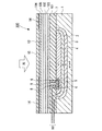
図1は、本発明の光電変換素子の第1実施形態を示す断面模式図である。また、図2は、第1実施形態の光電変換素子の変形例を示す断面模式図である。
図1に示す光電変換素子は、基板Sと、該基板S上に形成された下部電極(画素電極)101と、下部電極101上に形成された光電変換層102と、光電変換層102上に形成された電子ブロッキング層105と、電子ブロッキング層105上に形成された上部電極(対向電極)104とを備える。
(First embodiment)
FIG. 1 is a schematic cross-sectional view showing a first embodiment of the photoelectric conversion element of the present invention. FIG. 2 is a schematic cross-sectional view showing a modification of the photoelectric conversion element of the first embodiment.
The photoelectric conversion element shown in FIG. 1 includes a substrate S, a lower electrode (pixel electrode) 101 formed on the substrate S, a
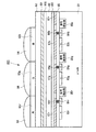
図2に示す光電変換素子は、基板Sと、該基板S上に形成された下部電極(画素電極)101と、下部電極101上に形成された正孔ブロッキング層103と、正孔ブロッキング層103上に形成された光電変換層102上に形成された上部電極(対向電極)104とを備える。なお、以下の説明においては、正孔ブロッキング層105と電子ブロッキング層103とを総称して、電荷ブロッキング層ともいう。
The photoelectric conversion element shown in FIG. 2 includes a substrate S, a lower electrode (pixel electrode) 101 formed on the substrate S, a
図1に示す光電変換素子は、上部電極104上方から光が入射するものとしている。また、光電変換素子は、光電変換層102で発生した電荷(正孔及び電子)のうち、電子を上部電極104に移動させ、正孔を下部電極101に移動させるように、下部電極101及び上部電極104間にバイアス電圧が印加されるものとしている。つまり、上部電極104を電子捕集電極とし、下部電極101を正孔捕集電極としている。
In the photoelectric conversion element shown in FIG. 1, light enters from above the
上部電極104は、光電変換層102に光を入射させる必要があるため、透明な導電性材料で構成されている。ここで、透明とは、例えば波長が約420nm〜約660nmの範囲の可視光を約80%以上透過することを言う。透明な導電性材料としてはITOを用いることが好ましい。
The
下部電極101は、導電性材料であればよく、透明である必要はない。しかし、図1に示す光電変換素子は、後述するが、下部電極101の下方にも光を透過させることが必要になる場合もあるため、下部電極101も透明な導電性材料で構成することが好ましい。上部電極104と同様に、下部電極101においてもITOを用いることが好ましい。
The
図1に示す光電変換素子は、光電変換層102と上部電極104との間に、一対の電極に電圧を印加した際に、電極からの電荷(ここでは、電子)注入に対して障壁となる電子ブロッキング層105が設けられている。電子ブロッキング層105は、上部電極104側から光電変換層102の方向にアモルファス層106と結晶層108とが交互に設けられてなる積層構造を有している。この光電変換素子においては、電子ブロッキング層105が応力緩衝層として機能する。
The photoelectric conversion element illustrated in FIG. 1 serves as a barrier against charge (here, electron) injection from the electrodes when a voltage is applied to the pair of electrodes between the
図2に示す光電変換素子は、画素電極101と光電変換層102との間に、一対の電極に電圧を印加した際に、電極からの電荷(ここでは正孔)注入に対して障壁となる正孔ブロッキング層103が設けられている。正孔ブロッキング層103は、画素電極101側から光電変換層102の方向にアモルファス層106と結晶層108とが交互に設けられてなる積層構造を有している。この光電変換素子においては、正孔ブロッキング層103が応力緩衝層として機能する。
The photoelectric conversion element illustrated in FIG. 2 becomes a barrier against charge (here, hole) injection from the electrodes when a voltage is applied to the pair of electrodes between the
光電変換層102は、光電変換機能を有する有機材料を含んで構成される。有機材料としては、例えば電子写真の感光材料に用いられているような、様々な有機半導体材料を用いることができる。その中でも、高い光電変換性能を有すること、分光する際の色分離に優れていること、長時間の光照射に対する耐久性が高いこと、真空蒸着を行いやすいこと、等の観点から、キナクリドン骨格を含む材料やフタロシアニン骨格を含む有機材料が特に好ましい。
The
光電変換層102として以下式で示されるキナクリドンを用いた場合には、光電変換層102にて緑色の波長域の光を吸収してこれに応じた電荷を発生することが可能となる。
When quinacridone represented by the following formula is used as the

光電変換層102として以下式で示される亜鉛フタロシアニンを用いた場合には、光電変換層102にて赤色の波長域の光を吸収してこれに応じた電荷を発生することが可能となる。
When zinc phthalocyanine represented by the following formula is used as the
また、光電変換層102を構成する有機材料は、有機p型半導体及び有機n型半導体の少なくとも一方を含んでいることが好ましい。有機p型半導体及び有機n型半導体として、それぞれキナクリドン誘導体、ナフタレン誘導体、アントラセン誘導体、フェナントレン誘導体、テトラセン誘導体、ピレン誘導体、ペリレン誘導体、及びフルオランテン誘導体のいずれかを特に好ましく用いることができる。
Moreover, it is preferable that the organic material which comprises the photoelectric converting
有機p型半導体(化合物)は、ドナー性有機半導体(化合物)であり、主に正孔輸送性有機化合物に代表され、電子を供与しやすい性質がある有機化合物をいう。さらに詳しくは2つの有機材料を接触させて用いたときにイオン化ポテンシャルの小さい方の有機化合物をいう。したがって、ドナー性有機化合物は、電子供与性のある有機化合物であればいずれの有機化合物も使用可能である。例えば、トリアリールアミン化合物、ベンジジン化合物、ピラゾリン化合物、スチリルアミン化合物、ヒドラゾン化合物、トリフェニルメタン化合物、カルバゾール化合物、ポリシラン化合物、チオフェン化合物、フタロシアニン化合物、シアニン化合物、メロシアニン化合物、オキソノール化合物、ポリアミン化合物、インドール化合物、ピロール化合物、ピラゾール化合物、ポリアリーレン化合物、縮合芳香族炭素環化合物(ナフタレン誘導体、アントラセン誘導体、フェナントレン誘導体、テトラセン誘導体、ピレン誘導体、ペリレン誘導体、フルオランテン誘導体)、含窒素ヘテロ環化合物を配位子として有する金属錯体等を用いることができる。なお、これに限らず、上記したように、n型(アクセプター性)化合物として用いた有機化合物よりもイオン化ポテンシャルの小さい有機化合物であればドナー性有機半導体として用いてよい。 The organic p-type semiconductor (compound) is a donor-type organic semiconductor (compound), which is mainly represented by a hole-transporting organic compound and refers to an organic compound having a property of easily donating electrons. More specifically, an organic compound having a smaller ionization potential when two organic materials are used in contact with each other. Therefore, any organic compound can be used as the donor organic compound as long as it is an electron-donating organic compound. For example, triarylamine compounds, benzidine compounds, pyrazoline compounds, styrylamine compounds, hydrazone compounds, triphenylmethane compounds, carbazole compounds, polysilane compounds, thiophene compounds, phthalocyanine compounds, cyanine compounds, merocyanine compounds, oxonol compounds, polyamine compounds, indoles Compounds, pyrrole compounds, pyrazole compounds, polyarylene compounds, condensed aromatic carbocyclic compounds (naphthalene derivatives, anthracene derivatives, phenanthrene derivatives, tetracene derivatives, pyrene derivatives, perylene derivatives, fluoranthene derivatives), nitrogen-containing heterocyclic compounds The metal complex etc. which it has as can be used. Not limited to this, as described above, any organic compound having an ionization potential smaller than that of the organic compound used as the n-type (acceptor property) compound may be used as the donor organic semiconductor.
有機n型半導体(化合物)は、アクセプター性有機半導体(化合物)であり、主に電子輸送性有機化合物に代表され、電子を受容しやすい性質がある有機化合物をいう。さらに詳しくは2つの有機化合物を接触させて用いたときに電子親和力の大きい方の有機化合物をいう。したがって、アクセプター性有機化合物は、電子受容性のある有機化合物であればいずれの有機化合物も使用可能である。例えば、縮合芳香族炭素環化合物(ナフタレン誘導体、アントラセン誘導体、フェナントレン誘導体、テトラセン誘導体、ピレン誘導体、ペリレン誘導体、フルオランテン誘導体)、窒素原子、酸素原子、硫黄原子を含有する5ないし7員のヘテロ環化合物(例えばピリジン、ピラジン、ピリミジン、ピリダジン、トリアジン、キノリン、キノキサリン、キナゾリン、フタラジン、シンノリン、イソキノリン、プテリジン、アクリジン、フェナジン、フェナントロリン、テトラゾール、ピラゾール、イミダゾール、チアゾール、オキサゾール、インダゾール、ベンズイミダゾール、ベンゾトリアゾール、ベンゾオキサゾール、ベンゾチアゾール、カルバゾール、プリン、トリアゾロピリダジン、トリアゾロピリミジン、テトラザインデン、オキサジアゾール、イミダゾピリジン、ピラリジン、ピロロピリジン、チアジアゾロピリジン、ジベンズアゼピン、トリベンズアゼピン等)、ポリアリーレン化合物、フルオレン化合物、シクロペンタジエン化合物、シリル化合物、含窒素ヘテロ環化合物を配位子として有する金属錯体などが挙げられる。なお、これに限らず、上記したように、ドナー性有機化合物として用いた有機化合物よりも電子親和力の大きな有機化合物であればアクセプター性有機半導体として用いてよい。 Organic n-type semiconductors (compounds) are acceptor organic semiconductors (compounds), which are mainly represented by electron-transporting organic compounds and refer to organic compounds that easily accept electrons. More specifically, the organic compound having the higher electron affinity when two organic compounds are used in contact with each other. Therefore, as the acceptor organic compound, any organic compound can be used as long as it is an electron-accepting organic compound. For example, condensed aromatic carbocyclic compounds (naphthalene derivatives, anthracene derivatives, phenanthrene derivatives, tetracene derivatives, pyrene derivatives, perylene derivatives, fluoranthene derivatives), 5- to 7-membered heterocyclic compounds containing nitrogen atoms, oxygen atoms, and sulfur atoms (E.g. pyridine, pyrazine, pyrimidine, pyridazine, triazine, quinoline, quinoxaline, quinazoline, phthalazine, cinnoline, isoquinoline, pteridine, acridine, phenazine, phenanthroline, tetrazole, pyrazole, imidazole, thiazole, oxazole, indazole, benzimidazole, benzotriazole, Benzoxazole, benzothiazole, carbazole, purine, triazolopyridazine, triazolopyrimidine, tetrazaindene, o Metal complexes having as ligands, such as sadiazole, imidazopyridine, pyralidine, pyrrolopyridine, thiadiazolopyridine, dibenzazepine, tribenzazepine), polyarylene compounds, fluorene compounds, cyclopentadiene compounds, silyl compounds, and nitrogen-containing heterocyclic compounds. Etc. Note that the present invention is not limited thereto, and as described above, any organic compound having an electron affinity higher than that of the organic compound used as the donor organic compound may be used as the acceptor organic semiconductor.
p型有機色素、又はn型有機色素としては、いかなるものを用いても良いが、好ましくは、シアニン色素、スチリル色素、ヘミシアニン色素、メロシアニン色素(ゼロメチンメロシアニン(シンプルメロシアニン)を含む)、3核メロシアニン色素、4核メロシアニン色素、ロダシアニン色素、コンプレックスシアニン色素、コンプレックスメロシアニン色素、アロポーラー色素、オキソノール色素、ヘミオキソノール色素、スクアリウム色素、クロコニウム色素、アザメチン色素、クマリン色素、アリーリデン色素、アントラキノン色素、トリフェニルメタン色素、アゾ色素、アゾメチン色素、スピロ化合物、メタロセン色素、フルオレノン色素、フルギド色素、ペリレン色素、フェナジン色素、フェノチアジン色素、キノン色素、インジゴ色素、ジフェニルメタン色素、ポリエン色素、アクリジン色素、アクリジノン色素、ジフェニルアミン色素、キナクリドン色素、キノフタロン色素、フェノキサジン色素、フタロペリレン色素、ポルフィリン色素、クロロフィル色素、フタロシアニン色素、金属錯体色素、縮合芳香族炭素環系色素(ナフタレン誘導体、アントラセン誘導体、フェナントレン誘導体、テトラセン誘導体、ピレン誘導体、ペリレン誘導体、フルオランテン誘導体)が挙げられる。 Any p-type organic dye or n-type organic dye may be used, but preferably a cyanine dye, a styryl dye, a hemicyanine dye, a merocyanine dye (including zero methine merocyanine (simple merocyanine)), three nuclei Merocyanine dye, 4-nuclear merocyanine dye, rhodacyanine dye, complex cyanine dye, complex merocyanine dye, allopolar dye, oxonol dye, hemioxonol dye, squalium dye, croconium dye, azamethine dye, coumarin dye, arylidene dye, anthraquinone dye, triphenyl Methane dye, azo dye, azomethine dye, spiro compound, metallocene dye, fluorenone dye, fulgide dye, perylene dye, phenazine dye, phenothiazine dye, quinone dye, indigo Dye, diphenylmethane dye, polyene dye, acridine dye, acridinone dye, diphenylamine dye, quinacridone dye, quinophthalone dye, phenoxazine dye, phthaloperylene dye, porphyrin dye, chlorophyll dye, phthalocyanine dye, metal complex dye, condensed aromatic carbocyclic dye (Naphthalene derivatives, anthracene derivatives, phenanthrene derivatives, tetracene derivatives, pyrene derivatives, perylene derivatives, fluoranthene derivatives).
次に金属錯体化合物について説明する。金属錯体化合物は金属に配位する少なくとも1つの窒素原子または酸素原子または硫黄原子を有する配位子をもつ金属錯体であり、金属錯体中の金属イオンは特に限定されないが、好ましくはベリリウムイオン、マグネシウムイオン、アルミニウムイオン、ガリウムイオン、亜鉛イオン、インジウムイオン、または錫イオンであり、より好ましくはベリリウムイオン、アルミニウムイオン、ガリウムイオン、または亜鉛イオンであり、更に好ましくはアルミニウムイオン、または亜鉛イオンである。前記金属錯体中に含まれる配位子としては種々の公知の配位子が有るが、例えば、「Photochemistry and Photophysics of Coordination Compounds」 Springer-Verlag社 H.Yersin著1987年発行、「有機金属化学−基礎と応用−」裳華房社山本明夫著1982年発行等に記載の配位子が挙げられる。 Next, the metal complex compound will be described. The metal complex compound is a metal complex having a ligand having at least one nitrogen atom or oxygen atom or sulfur atom coordinated to the metal, and the metal ion in the metal complex is not particularly limited, but preferably beryllium ion, magnesium Ion, aluminum ion, gallium ion, zinc ion, indium ion, or tin ion, more preferably beryllium ion, aluminum ion, gallium ion, or zinc ion, and still more preferably aluminum ion or zinc ion. As the ligand contained in the metal complex, there are various known ligands. For example, “Photochemistry and Photophysics of Coordination Compounds” published by Springer-Verlag H. Yersin in 1987, “Organometallic Chemistry— Examples of the ligands described in “Basics and Applications—” published by Akio Yamamoto, 1982, etc.
配位子として、好ましくは含窒素ヘテロ環配位子(好ましくは炭素数1〜30、より好ましくは炭素数2〜20、特に好ましくは炭素数3〜15であり、単座配位子であっても2座以上の配位子であってもよい。好ましくは2座配位子である。例えばピリジン配位子、ビピリジル配位子、キノリノール配位子、ヒドロキシフェニルアゾール配位子(ヒドロキシフェニルベンズイミダゾール、ヒドロキシフェニルベンズオキサゾール配位子、ヒドロキシフェニルイミダゾール配位子)などが挙げられる)、アルコキシ配位子(好ましくは炭素数1〜30、より好ましくは炭素数1〜20、特に好ましくは炭素数1〜10であり、例えばメトキシ、エトキシ、ブトキシ、2−エチルヘキシロキシなどが挙げられる。)、アリールオキシ配位子(好ましくは炭素数6〜30、より好ましくは炭素数6〜20、特に好ましくは炭素数6〜12であり、例えばフェニルオキシ、1−ナフチルオキシ、2−ナフチルオキシ、2,4,6−トリメチルフェニルオキシ、4−ビフェニルオキシなどが挙げられる。)、ヘテロアリールオキシ配位子(好ましくは炭素数1〜30、より好ましくは炭素数1〜20、特に好ましくは炭素数1〜12であり、例えばピリジルオキシ、ピラジルオキシ、ピリミジルオキシ、キノリルオキシなどが挙げられる。)、アルキルチオ配位子(好ましくは炭素数1〜30、より好ましくは炭素数1〜20、特に好ましくは炭素数1〜12であり、例えばメチルチオ、エチルチオなどが挙げられる。)、アリールチオ配位子(好ましくは炭素数6〜30、より好ましくは炭素数6〜20、特に好ましくは炭素数6〜12であり、例えばフェニルチオなどが挙げられる。)、ヘテロ環置換チオ配位子(好ましくは炭素数1〜30、より好ましくは炭素数1〜20、特に好ましくは炭素数1〜12であり、例えばピリジルチオ、2−ベンズイミゾリルチオ、2−ベンズオキサゾリルチオ、2−ベンズチアゾリルチオなどが挙げられる。)、またはシロキシ配位子(好ましくは炭素数1〜30、より好ましくは炭素数3〜25、特に好ましくは炭素数6〜20であり、例えば、トリフェニルシロキシ基、トリエトキシシロキシ基、トリイソプロピルシロキシ基などが挙げられる)であり、より好ましくは含窒素ヘテロ環配位子、アリールオキシ配位子、ヘテロアリールオキシ基、またはシロキシ配位子であり、更に好ましくは含窒素ヘテロ環配位子、アリールオキシ配位子、またはシロキシ配位子が挙げられる。 The ligand is preferably a nitrogen-containing heterocyclic ligand (preferably having 1 to 30 carbon atoms, more preferably 2 to 20 carbon atoms, particularly preferably 3 to 15 carbon atoms, and a monodentate ligand. May also be a bidentate or higher ligand, preferably a bidentate ligand, such as a pyridine ligand, a bipyridyl ligand, a quinolinol ligand, a hydroxyphenylazole ligand (hydroxyphenylbenz). Imidazole, hydroxyphenylbenzoxazole ligand, hydroxyphenylimidazole ligand)), alkoxy ligand (preferably having 1 to 30 carbon atoms, more preferably 1 to 20 carbon atoms, and particularly preferably carbon number). 1 to 10, for example, methoxy, ethoxy, butoxy, 2-ethylhexyloxy, etc.), aryloxy ligand (preferably Alternatively, it has 6 to 30 carbon atoms, more preferably 6 to 20 carbon atoms, and particularly preferably 6 to 12 carbon atoms. For example, phenyloxy, 1-naphthyloxy, 2-naphthyloxy, 2,4,6-trimethylphenyl Oxy, 4-biphenyloxy, etc.), heteroaryloxy ligands (preferably having 1 to 30 carbon atoms, more preferably 1 to 20 carbon atoms, particularly preferably 1 to 12 carbon atoms, such as pyridyl. Oxy, pyrazyloxy, pyrimidyloxy, quinolyloxy, etc.), alkylthio ligands (preferably having 1 to 30 carbon atoms, more preferably 1 to 20 carbon atoms, particularly preferably 1 to 12 carbon atoms, such as methylthio, Ethylthio etc.), an arylthio ligand (preferably having 6 to 30 carbon atoms, more preferably A prime number of 6 to 20, particularly preferably 6 to 12 carbon atoms, such as phenylthio, and the like, a heterocyclic substituted thio ligand (preferably 1 to 30 carbon atoms, more preferably 1 to 20 carbon atoms, Particularly preferably, it has 1 to 12 carbon atoms, and examples thereof include pyridylthio, 2-benzimidazolylthio, 2-benzoxazolylthio, 2-benzthiazolylthio and the like, or siloxy ligand (preferably carbon 1-30, more preferably 3-25 carbon atoms, particularly preferably 6-20 carbon atoms, and examples thereof include triphenylsiloxy group, triethoxysiloxy group, triisopropylsiloxy group, and the like. Preferred are nitrogen-containing heterocyclic ligands, aryloxy ligands, heteroaryloxy groups, or siloxy ligands, and more preferred. Examples thereof include a nitrogen-containing heterocyclic ligand, an aryloxy ligand, and a siloxy ligand.
応力緩衝層は、その少なくとも一部に結晶層を含む積層構造とすることができる。図1及び図2に示す光電変換素子では、電子ブロッキング層105又は正孔ブロッキング層103の一部を結晶層を含む積層構造として応力緩衝層としてもよい。応力緩衝層は、一対の電極101,104のうち一方と光電変換層102とに挟まれた部位に少なくとも一つ設けられればよく、電子ブロッキング層105又は正孔ブロッキング層103に限定されず、それ以外の層や該層の一部に設けてもよい。また、応力緩衝層は、画素電極101と光電変換層102との間、及び、光電変換層102と上部電極104との間にそれぞれ設けられていてよい。
The stress buffer layer can have a laminated structure including a crystal layer in at least a part thereof. In the photoelectric conversion element shown in FIGS. 1 and 2, a part of the
応力緩衝層に用いる結晶層は、単結晶より粒界や隙間をもつ微結晶性であることが好ましい。結晶層は、アモルファス層との界面において、結晶の粒界や隙間により応力を吸収できるのではないかと考えられる。ここで、微結晶とは、有機材料や無機材料を抵抗加熱蒸着や電子ビーム蒸着、スパッタ、CVD(Chemical Vapor Deposition)、塗布などで作製した薄膜において、アモルファス層を構成するアモルファス成分に対して結晶体積分率が数%から100%であり、また結晶粒径が数オングストロームから数μmとなるもの指す。応力緩衝層に含まれる結晶層とアモルファス層の厚みがそれぞれ0.5〜200nmであることが好ましい。 The crystal layer used for the stress buffer layer is preferably microcrystalline with grain boundaries and gaps rather than single crystals. The crystal layer is considered to be able to absorb stress at the interface with the amorphous layer due to crystal grain boundaries and gaps. Here, the microcrystal is a crystal formed with respect to an amorphous component constituting an amorphous layer in a thin film produced by resistance heating vapor deposition, electron beam vapor deposition, sputtering, CVD (Chemical Vapor Deposition), coating, or the like of an organic material or an inorganic material. The volume fraction is from several% to 100%, and the crystal grain size is from several angstroms to several micrometers. The thickness of the crystal layer and the amorphous layer included in the stress buffer layer is preferably 0.5 to 200 nm, respectively.
結晶層を構成する材料は、電荷輸送性を有し微結晶性となる材料が好ましい。有機材料では平面性が高く分子間力が大きい材料は結晶性を発現しやすく、たとえば有機顔料などがあげられる。また、室温で成膜した場合にアモルファス層を構成する材料であっても、基板加熱等の加熱成膜により微結晶性となる材料であれば用いることができる。無機材料は成膜時に微結晶性となるものが多く、必要な電荷輸送性があればさまざまな材料を用いることができ、特に、電荷輸送性とブロッキング性を有する無機酸化物などが好ましい。 The material constituting the crystal layer is preferably a material that has charge transportability and becomes microcrystalline. Among organic materials, a material having high planarity and a large intermolecular force tends to exhibit crystallinity, and examples thereof include organic pigments. Moreover, even if it is a material which comprises an amorphous layer when it forms into a film at room temperature, if it becomes a material which becomes microcrystallinity by heating film-forming, such as a substrate heating, it can be used. Many inorganic materials become microcrystalline at the time of film formation, and various materials can be used as long as they have necessary charge transport properties. In particular, inorganic oxides having charge transport properties and blocking properties are preferable.
アモルファス層を構成するアモルファス材料としては、電荷輸送性があれば一般的に知られている有機材料と無機材料いずれも用いることができる。また、室温での成膜で微結晶性となる材料でも、基板冷却などによりアモルファス層を形成することが可能であれば、用いることが可能である。また、結晶層と積層構造を構成する層としては、アモルファス層に限定されず、該結晶層との界面で結晶の粒界や隙間により応力を吸収できる層であれば、他の材料からなる層を適用することができる。 As the amorphous material constituting the amorphous layer, any generally known organic material and inorganic material can be used as long as they have charge transport properties. A material that becomes microcrystalline when deposited at room temperature can be used as long as the amorphous layer can be formed by cooling the substrate or the like. Further, the layer constituting the laminated structure with the crystal layer is not limited to an amorphous layer, and a layer made of another material as long as stress can be absorbed by crystal grain boundaries and gaps at the interface with the crystal layer. Can be applied.
図1及び図2に示す光電変換素子において、電子ブロッキング層105と正孔ブロッキング層103の両方を備えた構成としてもよい。電圧を印加する方向に応じて電子ブロッキング層105と正孔ブロッキング層103を入れ替えた構成としてもよい。
The photoelectric conversion element illustrated in FIGS. 1 and 2 may be configured to include both the
光電変換の効率を良くするために、上部電極104と下部電極101との間に外部から印加される電圧を、電極101,104間の距離で割った値が1.0×10⁵V/cm〜1.0×107V/cmであることが好ましい。
In order to improve the efficiency of photoelectric conversion, a value obtained by dividing an externally applied voltage between the
電荷ブロッキング層の膜厚は、薄すぎると十分なブロッキング性を確保することができず、逆に厚すぎると光電変換層にかかる電界が小さくなるため効率の低下を招いてしまうので、0.01〜15μmであることが好ましい。より好ましくは、0.03〜1μm、さらに好ましくは、0.05〜0.2μmである。 If the film thickness of the charge blocking layer is too thin, sufficient blocking properties cannot be ensured. Conversely, if the film is too thick, the electric field applied to the photoelectric conversion layer is reduced, resulting in a decrease in efficiency. It is preferable that it is ˜15 μm. More preferably, it is 0.03-1 micrometer, More preferably, it is 0.05-0.2 micrometer.
本実施形態の光電変換素子によれば、電極101,104と光電変換層102との間に、結晶層108を含む積層構造である応力緩衝層を備えおり、電極で生じた応力を応力緩衝層によって緩衝することができる。このため、電極101,104と光電変換層102との界面で亀裂、剥れ、変形などが生じることを防止することができる。また、応力緩衝層を設けることで、電極の厚さを薄くする構成とする必要がなく、電極の抵抗値の増加による電圧降下や応答速度の低下などの不具合が生じることを回避できる。
According to the photoelectric conversion element of this embodiment, the stress buffer layer having a laminated structure including the crystal layer 108 is provided between the
電極と電荷ブロッキング層との間に応力緩衝層を設ける構成とすれば、電極と電荷ブロッキング層との界面で亀裂、剥れ、変形などが生じることを防止することができる。 If a stress buffer layer is provided between the electrode and the charge blocking layer, it is possible to prevent cracks, peeling, deformation, and the like from occurring at the interface between the electrode and the charge blocking layer.
以下の第2実施形態〜第5実施形態では、上述したような光電変換素子を半導体基板上方に積層した構成のセンサとしてあげられる構成例を説明する。なお、以下に説明する実施形態において、すでに説明した部材などと同等な構成・作用を有する部材等については、図中に同一符号又は相当符号を付すことにより、説明を簡略化或いは省略する。 In the following second to fifth embodiments, description will be given of configuration examples that can be cited as sensors having a configuration in which the photoelectric conversion elements as described above are stacked above a semiconductor substrate. In the embodiments described below, members having the same configuration / action as those already described are denoted by the same or corresponding reference numerals in the drawings, and description thereof is simplified or omitted.
(第2実施形態)
図3は、本発明の第2実施形態を説明するための固体撮像素子の1画素分の断面模式図である。図3において図1及び図2と同等の構成には同一符号を付してある。
固体撮像素子100は、図3に示す1画素が同一平面上でアレイ状に多数配置されたものであり、この1画素から得られる信号によって画像データの1つの画素データを生成することができる。
(Second Embodiment)
FIG. 3 is a schematic cross-sectional view of one pixel of a solid-state image sensor for explaining the second embodiment of the present invention. 3, the same components as those in FIGS. 1 and 2 are denoted by the same reference numerals.
The solid-
図3に示す固体撮像素子の1画素は、p型シリコン基板1と、p型シリコン基板1上に形成された透明な絶縁膜7と、絶縁膜7上に形成された下部電極101、下部電極101上に形成された正孔ブロッキング層103と、正孔ブロッキング層103上に形成された光電変換層102と、光電変換層102上に形成された電子ブロッキング層105と、電子ブロッキング層105上に形成された上部電極104からなる構成の光電変換素子とを含んで構成され、光電変換素子上には開口の設けられた遮光膜14が形成されている。上部電極104上には透明な絶縁膜15が形成されている。ここで、電子ブロッキング層105及び正孔ブロッキング層103のうち少なくとも一方に、結晶層を含む積層構造である応力緩衝層が設けられている。
One pixel of the solid-state imaging device shown in FIG. 3 includes a p-type silicon substrate 1, a transparent
p型シリコン基板1内には、その浅い方からn型不純物領域(以下、n領域と略す)4と、p型不純物領域(以下、p領域と略す)3と、n領域2がこの順に形成されている。n領域4の遮光膜14によって遮光されている部分の表面部には、高濃度のn領域(n+領域という)6が形成され、n+領域6の周りはp領域5によって囲まれている。
In the p-type silicon substrate 1, an n-type impurity region (hereinafter abbreviated as n region) 4, a p-type impurity region (hereinafter abbreviated as p region) 3, and an
n領域4とp領域3とのpn接合面のp型シリコン基板1表面からの深さは、青色光を吸収する深さ(約0.2μm)となっている。したがって、n領域4とp領域3は、青色光を吸収してそれに応じた電荷を蓄積するフォトダイオード(Bフォトダイオード)を形成する。
The depth of the pn junction surface between the
n領域2とp型シリコン基板1とのpn接合面のp型シリコン基板1表面からの深さは、赤色光を吸収する深さ(約2μm)となっている。したがって、n領域2とp型シリコン基板1は、赤色光を吸収してそれに応じた電荷を蓄積するフォトダイオード(Rフォトダイオード)を形成する。
The depth of the pn junction surface between the
n+領域6は、絶縁膜7に開けられた開口に形成された接続部9を介して下部電極101と電気的に接続されている。下部電極101で捕集された正孔は、n+領域6の電子と再結合するため、捕集した正孔の数に応じ、n+領域6にリセット時に蓄積された電子が減少することとなる。接続部9は、下部電極101とn+領域6以外とは絶縁膜8によって電気的に絶縁される。
The n + region 6 is electrically connected to the
n領域2に蓄積された電子は、p型シリコン基板1内に形成されたnチャネルMOSトランジスタからなるMOS回路(不図示)によってその電荷量に応じた信号に変換され、n領域4に蓄積された電子は、p領域3内に形成されたnチャネルMOSトランジスタからなるMOS回路(不図示)によってその電荷量に応じた信号に変換され、n+領域6に蓄積されている電子は、p領域5内に形成されたnチャネルMOSトランジスタからなるMOS回路(不図示)によってその電荷量に応じた信号に変換されて、固体撮像素子100外部へと出力される。各MOS回路は配線10によって図示しない信号読み出しパッドに接続される。なお、n領域2、n領域4に引き出し電極を設け、所定のリセット電位をかけると、各領域が空乏化し、各pn接合部の容量は限りなく小さい値になる。これにより、接合面に生じる容量を極めて小さくすることができる。
The electrons accumulated in the
このような構成により、光電変換層102でG光を光電変換し、p型シリコン基板1中のBフォトダイオードとRフォトダイオードでB光およびR光を光電変換することができる。また上部でG光がまず吸収されるため、B−G間およびG−R間の色分離は優れている。これが、シリコン基板内に3つのPDを積層し、シリコン基板内でBGR光を全て分離する形式の固体撮像素子に比べ、大きく優れた点である。
With such a configuration, G light can be photoelectrically converted by the
本実施形態の固体撮像素子100は、画素電極101及び上部電極104と光電変換層102との間に少なくとも1つの応力緩衝層を備えた構成である。このため、電極101,104で生じた応力を応力緩衝層によって緩衝することができ、電極101,104と光電変換層102との界面で亀裂、剥れ、変形などが生じることを防止できる。
The solid-
(第3実施形態)
本実施形態では、図3のシリコン基板1内に2つのフォトダイオードを積層するのではなく、入射光の入射方向に対して垂直な方向に2つのフォトダイオードを配列して、p型シリコン基板内で2色の光を検出するようにしたものである。
(Third embodiment)
In the present embodiment, two photodiodes are not stacked in the silicon substrate 1 of FIG. 3, but two photodiodes are arranged in a direction perpendicular to the incident direction of incident light, and the p-type silicon substrate Thus, two colors of light are detected.
図4は、本発明の第3実施形態を説明するための固体撮像素子の1画素分の断面模式図である。図4において図1と同等の構成には同一符号を付してある。
図4に示す固体撮像素子200の1画素は、p型シリコン基板17と、p型シリコン基板17上方に形成された下部電極101、下部電極101上に形成された正孔ブロッキング層103と、該正孔ブロッキング層103上に形成された光電変換層102と、該光電変換層102上に形成された電子ブロッキング層105と、電子ブロッキング層105上に形成された上部電極104とを備えた構成の光電変換素子とを含んで構成され、光電変換素子上には開口の設けられた遮光膜34が形成されている。また、上部電極104上には透明な絶縁膜33が形成されている。ここで、電子ブロッキング層105及び正孔ブロッキング層103のうち少なくとも一方に、結晶層を含む積層構造である応力緩衝層が設けられている。
FIG. 4 is a schematic cross-sectional view of one pixel of a solid-state image sensor for explaining the third embodiment of the present invention. In FIG. 4, the same components as those in FIG.
One pixel of the solid-
遮光膜34の開口下方のp型シリコン基板17表面には、p領域19とn領域18からなるフォトダイオードと、p領域21とn領域20からなるフォトダイオードとが、p型シリコン基板17表面に並んで形成されている。p型シリコン基板17表面上の任意の面方向が、入射光の入射方向に対して垂直な方向となる。
On the surface of the p-
p領域19とn領域18からなるフォトダイオードの上方には、透明な絶縁膜24を介してB光を透過するカラーフィルタ28が形成され、その上に下部電極101が形成されている。p領域21とn領域20からなるフォトダイオードの上方には、透明な絶縁膜24を介してR光を透過するカラーフィルタ29が形成され、その上に下部電極101が形成されている。カラーフィルタ28,29の周囲は、透明な絶縁膜25で覆われている。
Above the photodiode composed of the
p領域19とn領域18からなるフォトダイオードは、カラーフィルタ28を透過したB光を吸収してそれに応じた電子を発生し、発生した電子をn領域18に蓄積する基板内光電変換部として機能する。p領域21とn領域20からなるフォトダイオードは、カラーフィルタ29を透過したR光を吸収してそれに応じた電子を発生し、発生した電子をn領域20に蓄積する基板内光電変換部として機能する。
The photodiode composed of the
n型シリコン基板17表面の遮光膜34によって遮光されている部分には、n+領域23が形成され、n+領域23の周りはp領域22によって囲まれている。
An n +
n+領域23は、絶縁膜24,25に開けられた開口に形成された接続部27を介して下部電極101と電気的に接続されている。下部電極101で捕集された正孔は、n+領域23の電子と再結合するため、捕集した正孔の数に応じ、n+領域23にリセット時に蓄積された電子が減少することとなる。接続部27は、下部電極101とn+領域23以外とは絶縁膜26によって電気的に絶縁される。
The n +
n領域18に蓄積された電子は、p型シリコン基板17内に形成されたnチャネルMOSトランジスタからなるMOS回路(不図示)によってその電荷量に応じた信号に変換され、n領域20に蓄積された電子は、p型シリコン基板17内に形成されたnチャネルMOSトランジスタからなるMOS回路(不図示)によってその電荷量に応じた信号に変換され、n+領域23に蓄積されている電子は、p領域22内に形成されたnチャネルMOSトランジスタからなるMOS回路(不図示)によってその電荷量に応じた信号に変換されて、固体撮像素子200外部へと出力される。各MOS回路は配線35によって図示しない信号読み出しパッドに接続される。
なお、信号読出し部は、MOS回路ではなくCCDとアンプによって構成してもよい。つまり、n領域18、n領域20、及びn+領域23に蓄積された電子をp型シリコン基板17内に形成したCCDに読み出し、これをCCDでアンプまで転送して、アンプからその電子に応じた信号を出力させるような信号読出し部であってもよい。
The electrons accumulated in the
The signal reading unit may be constituted by a CCD and an amplifier instead of the MOS circuit. That is, the electrons accumulated in the
このように、信号読み出し部は、CCDおよびCMOS構造が挙げられるが、消費電力、高速読出し、画素加算、部分読出し等の点からは、CMOSの方が好ましい。 As described above, the signal reading unit includes a CCD and a CMOS structure, but CMOS is preferable in terms of power consumption, high-speed reading, pixel addition, partial reading, and the like.
なお、図4では、カラーフィルタ28,29によってR光とB光の色分離を行っているが、カラーフィルタ28,29を設けず、n領域20とp領域21のpn接合面の深さと、n領域18とp領域19のpn接合面の深さを各々調整して、それぞれのフォトダイオードでR光とB光を吸収するようにしてもよい。
In FIG. 4, the
p型シリコン基板17と下部電極101との間(例えば絶縁膜24とp型シリコン基板17との間)に、光電変換層102を透過した光を吸収して、該光に応じた電荷を発生しこれを蓄積する無機材料からなる無機光電変換部を形成することも可能である。この場合、p型シリコン基板17内に、この無機光電変換部の電荷蓄積領域に蓄積された電荷に応じた信号を読み出すためのMOS回路を設け、このMOS回路にも配線35を接続しておけばよい。
Light that has passed through the
また、p型シリコン基板17内に設けるフォトダイオードを1つとし、p型シリコン基板17上方に光電変換部を複数積層した構成としてもよい。更に、p型シリコン基板17内に設けるフォトダイオードを複数とし、p型シリコン基板17上方に光電変換部を複数積層した構成としてもよい。また、カラー画像を作る必要がないのであれば、p型シリコン基板17内に設けるフォトダイオードを1つとし、光電変換部を1つだけ積層した構成としてもよい。
Alternatively, a single photodiode may be provided in the p-
本実施形態の固体撮像素子200は、画素電極101及び上部電極104と光電変換層102との間に少なくとも1つの応力緩衝層を備えた構成である。このため、電極101,104で生じた応力を応力緩衝層によって緩衝することができ、電極101,104と光電変換層102との界面で亀裂、剥れ、変形などが生じることを防止できる。
The solid-
(第4実施形態)
本実施形態の固体撮像素子は、シリコン基板内にフォトダイオードを設けず、シリコン基板上方に複数(ここでは3つ)の光電変換素子を積層した構成である。
図5は、本発明の第4実施形態を説明するための固体撮像素子の1画素分の断面模式図である。
図5に示す固体撮像素子300は、R光電変換素子と、B光電変換素子と、G光電変換素子とをシリコン基板41の上方に順に積層した構成である。
R光電変換素子は、シリコン基板41上方に、下部電極101r、下部電極101r上に形成された正孔ブロッキング層103r,該正孔ブロッキング層103上に積層された光電変換層102r、該光電変換層102r上に形成された電子ブロッキング層105r、該電子ブロッキング層105r上に積層された上部電極104rを含む。正孔ブロッキング層103r及び電子ブロッキング層105rのうち少なくとも一方を応力緩衝層とする。
(Fourth embodiment)
The solid-state imaging device of this embodiment has a configuration in which a photodiode is not provided in a silicon substrate, and a plurality of (here, three) photoelectric conversion elements are stacked above the silicon substrate.
FIG. 5 is a schematic cross-sectional view of one pixel of a solid-state image sensor for explaining a fourth embodiment of the present invention.
A solid-
The R photoelectric conversion element has a
B光電変換素子は、下部電極101b、下部電極101b上に形成された正孔ブロッキング層103b,該正孔ブロッキング層103b上に積層された光電変換層102b、該光電変換層102b上に形成された電子ブロッキング層105b、該電子ブロッキング層105b上に積層された上部電極104bを含む。正孔ブロッキング層103b及び電子ブロッキング層105bのうち少なくとも一方を応力緩衝層とする。
The B photoelectric conversion element was formed on the
G光電変換素子は、下部電極101g、下部電極101g上に形成された正孔ブロッキング層103g,該正孔ブロッキング層103g上に積層された光電変換層102g、該光電変換層102g上に形成された電子ブロッキング層105g、該電子ブロッキング層105g上に積層された上部電極104gを含む。R光電変換素子とB光電変換素子とG光電変換素子とが、それぞれに含まれる下部電極をシリコン基板41側に向けた状態で、この順に積層された構成となっている。正孔ブロッキング層103g及び電子ブロッキング層105gのうち少なくとも一方を応力緩衝層とする。
The G photoelectric conversion element was formed on the
R光電変換素子の上部電極104rとB光電変換素子の下部電極101bとの間に透明な絶縁膜59が形成され、B光電変換素子の上部電極104bとG光電変換素子の下部電極101gとの間に透明な絶縁膜63が形成されている。G光電変換素子の上部電極104g上には、開口を除く領域に遮光膜68が形成され、該上部電極104gと遮光膜68を覆うように透明な絶縁膜67が形成されている。
A transparent insulating
R,G,Bの各光電変換素子に含まれる下部電極、光電変換層、正孔ブロッキング層、電子ブロッキング層、及び上部電極は、それぞれ、図1に示す光電変換素子のものと同じ構成とすることができる。ただし、光電変換層102gは、緑色光を吸収してこれに応じた電子及び正孔を発生する有機材料を含むものとし、光電変換層102bは、青色光を吸収してこれに応じた電子及び正孔を発生する有機材料を含むものとし、光電変換層102rは、赤色光を吸収してこれに応じた電子及び正孔を発生する有機材料を含むものとする。
The lower electrode, the photoelectric conversion layer, the hole blocking layer, the electron blocking layer, and the upper electrode included in each of the R, G, and B photoelectric conversion elements have the same configuration as that of the photoelectric conversion element shown in FIG. be able to. However, the
シリコン基板41表面の遮光膜68によって遮光されている部分には、n+領域43,45,47が形成され、それぞれの周りはp領域42,44,46によって囲まれている。
N +
n+領域43は、絶縁膜48に開けられた開口に形成された接続部54を介して下部電極101rと電気的に接続されている。下部電極101rで捕集された正孔は、n+領域43の電子と再結合するため、捕集した正孔の数に応じ、n+領域43にリセット時に蓄積された電子が減少することとなる。接続部54は、下部電極101rとn+領域43以外とは絶縁膜51によって電気的に絶縁される。
The n +
n+領域45は、絶縁膜48、R光電変換素子、及び絶縁膜59に開けられた開口に形成された接続部53を介して下部電極101bと電気的に接続されている。下部電極101bで捕集された正孔は、n+領域45の電子と再結合するため、捕集した正孔の数に応じ、n+領域45にリセット時に蓄積された電子が減少することとなる。接続部53は、下部電極101bとn+領域45以外とは絶縁膜50によって電気的に絶縁される。
The n +
n+領域47は、絶縁膜48、R光電変換素子、絶縁膜59、B光電変換素子、及び絶縁膜63に開けられた開口に形成された接続部52を介して下部電極101gと電気的に接続されている。下部電極101gで捕集された正孔は、n+領域47の電子と再結合するため、捕集した正孔の数に応じ、n+領域47にリセット時に蓄積された電子が減少することとなる。接続部52は、下部電極101gとn+領域47以外とは絶縁膜49によって電気的に絶縁される。
The n +
n+領域43に蓄積されている電子は、p領域42内に形成されたnチャネルMOSトランジスタからなるMOS回路(不図示)によってその電荷量に応じた信号に変換され、n+領域45に蓄積されている電子は、p領域44内に形成されたnチャネルMOSトランジスタからなるMOS回路(不図示)によってその電荷量に応じた信号に変換され、n+領域47に蓄積されている電子は、p領域46内に形成されたnチャネルMOSトランジスタからなるMOS回路(不図示)によってその電荷量に応じた信号に変換されて、固体撮像素子300外部へと出力される。各MOS回路は配線55によって図示しない信号読み出しパッドに接続される。なお、信号読出し部は、MOS回路ではなくCCDとアンプによって構成してもよい。つまり、n+領域43,45,47に蓄積された電子をシリコン基板41内に形成したCCDに読み出し、これをCCDでアンプまで転送して、アンプからその正孔に応じた信号を出力させるような信号読出し部であってもよい。
The electrons accumulated in the n +
以上の説明において、B光を吸収する光電変換層とは、例えば、少なくとも400〜500nmの光を吸収することができ、好ましくはその波長域でのピ−ク波長の吸収率が50%以上であるものを意味する。G光を吸収する光電変換層とは、例えば、少なくとも500〜600nmの光を吸収することができ、好ましくはその波長域でのピ−ク波長の吸収率が50%以上であることを意味する。R光を吸収する光電変換層とは、例えば、少なくとも600〜700nmの光を吸収することができ、好ましくはその波長域でのピ−ク波長の吸収率が50%以上であることを意味する。 In the above description, the photoelectric conversion layer that absorbs B light can, for example, absorb light of at least 400 to 500 nm, and preferably has a peak wavelength absorptance of 50% or more in that wavelength region. It means something. The photoelectric conversion layer that absorbs G light means, for example, that it can absorb light of at least 500 to 600 nm, and preferably has a peak wavelength absorptance of 50% or more in that wavelength region. . The photoelectric conversion layer that absorbs R light means, for example, that it can absorb light of at least 600 to 700 nm, and preferably has a peak wavelength absorptance of 50% or more in that wavelength region. .
本実施形態の固体撮像素子300は、積層された各光電変換素子の画素電極101r,101g,101b及び上部電極104r,104g,104bと光電変換層102r,102g,102bとの間に応力緩衝層を備えた構成である。このため、画素電極101r,101g,101b及び上部電極104r,104g,104bで生じた応力を応力緩衝層によって緩衝することができ、画素電極101r,101g,101b及び上部電極104r,104g,104bと光電変換層102r,102g,102bと間のそれぞれの界面で亀裂、剥れ、変形などが生じることを防止できる。
In the solid-
(第5実施形態)
図6は、本発明の第5実施形態を説明するための固体撮像素子の断面模式図である。
p型シリコン基板81上方の同一面上の行方向とこれに直交する列方向には、主としてRの波長域の光を透過するカラーフィルタ93rと、主としてGの波長域の光を透過するカラーフィルタ93gと、主としてBの波長域の光を透過するカラーフィルタ93bとの3種類のカラーフィルタがそれぞれ多数配列されている。
(Fifth embodiment)
FIG. 6 is a schematic cross-sectional view of a solid-state imaging device for explaining a fifth embodiment of the present invention.
In the row direction on the same plane above the p-
カラーフィルタ93rは、公知の材料を用いることができるが、このような材料は、Rの波長域の光の他に、赤外域の光の一部も透過する。カラーフィルタ93gは、公知の材料を用いることができるが、このような材料は、Gの波長域の光の他に、赤外域の光の一部も透過する。カラーフィルタ93bは、公知の材料を用いることができるが、このような材料は、Bの波長域の光の他に、赤外域の光の一部も透過する。
A known material can be used for the
カラーフィルタ93r,93g,93bの配列は、公知の単板式固体撮像素子に用いられているカラーフィルタ配列(ベイヤー配列や縦ストライプ、横ストライプ等)を採用することができる。
As the arrangement of the
カラーフィルタ93r下方には、カラーフィルタ93rに対応させてn型不純物領域(以下、n領域という)83rが形成されており、n領域83rとp型シリコン基板81とのpn接合によって、カラーフィルタ93rに対応するR光電変換素子が構成されている。
Below the
カラーフィルタ93g下方には、カラーフィルタ93gに対応させてn領域83gが形成されており、n領域83gとp型シリコン基板81とのpn接合によって、カラーフィルタ93gに対応するG光電変換素子が構成されている。
Below the
カラーフィルタ93b下方には、カラーフィルタ93bに対応させてn領域83bが形成されており、n領域83bとp型シリコン基板81とのpn接合によって、カラーフィルタ93bに対応するB光電変換素子が構成されている。
An
n領域83r上方には下部電極87r(図1の下部電極101と同じ機能を持つ)が形成され、n領域83g上方には下部電極87g(図1の下部電極101と同じ機能を持つ)が形成され、n領域83b上方には下部電極87b(図1の下部電極101と同じ機能を持つ)が形成されている。下部電極87r,87g,87bは、それぞれカラーフィルタ93r,93g,93bの各々に対応して分割されている。下部電極87r,87g,87bは、それぞれ、可視光及び赤外光に対して透明な材料で構成され、例えばITO(Indium Tin Oxide)やIZO(Indium Zico Oxide)等を用いることができる。下部電極87r,87g,87bは、それぞれ、絶縁層内に埋設されている。
A
下部電極87r,87g,87bの各々の上には、主として波長580nm以上の赤外域の光を吸収してこれに応じた電荷を発生し、赤外域以外の可視域(例えば波長約380nm〜約580nm)の光を透過する、カラーフィルタ93r,93g,93bの各々で共通の一枚構成である光電変換層89(図1の光電変換層102と同じ機能を持つ)が形成されている。光電変換層89を構成する材料は、例えば、フタロシアニン系有機材料やナフタロシアニン系有機材料を用いる。
On each of the
光電変換層89上には、カラーフィルタ93r,93g,93bの各々で共通の一枚構成である上部電極80(図1の上部電極104と同じ機能を持つ)が形成されている。上部電極80は、可視光及び赤外光に対して透明な材料で構成され、例えばITOやIZO等を用いることができる。光電変換層89と上部電極80との間には、図1の電子ブロッキング層105と同じ機能を持つ電子ブロッキング層が形成されている。下部電極87r,87g,87bと、光電変換層89との間にはそれぞれ、図示しない正孔ブロッキング層103が形成されている。正孔ブロッキング層103及び電子ブロッキング層105のうち少なくとも一方を応力緩衝層とする。
On the
下部電極87rと、それに対向する上部電極80と、これらに挟まれる光電変換層89の一部とにより、カラーフィルタ93rに対応する光電変換素子が形成される。以下では、この光電変換素子を、半導体基板上に形成されたものであるため、R基板上光電変換素子という。下部電極87gと、それに対向する上部電極80と、これらに挟まれる光電変換層89の一部とにより、カラーフィルタ93gに対応する光電変換素子が形成される。以下では、この光電変換素子をG基板上光電変換素子という。下部電極87bと、それに対向する上部電極80と、これらに挟まれる光電変換層89の一部とにより、カラーフィルタ93bに対応する光電変換素子が形成される。以下では、この光電変換素子をB基板上光電変換素子という。
A photoelectric conversion element corresponding to the
n領域83rの隣には、R基板上光電変換素子の下部電極87rと接続された高濃度のn型不純物領域(以下、n+領域という)84rが形成されている。尚、n+領域84rに光が入るのを防ぐために、n+領域84r上には遮光膜を設けておくことが好ましい。
Next to the
n領域83gの隣には、G基板上光電変換素子の下部電極87gと接続されたn+領域84gが形成されている。なお、n+領域84gに光が入るのを防ぐために、n+領域84g上には遮光膜を設けておくことが好ましい。
Next to the
n領域83bの隣には、B基板上光電変換素子の下部電極87bと接続されたn+領域84bが形成されている。なお、n+領域84bに光が入るのを防ぐために、n+領域84b上には遮光膜を設けておくことが好ましい。
Next to the
n+領域84r上にはタングステン、アルミニウム等の金属からなるコンタクト部86rが形成され、コンタクト部86r上に下部電極87rが形成されており、n+領域84rと下部電極87rはコンタクト部86rによって電気的に接続されている。コンタクト部86rは、可視光及び赤外光に対して透明な絶縁層85内に埋設されている。
A
n+領域84g上にはタングステン、アルミニウム等の金属からなるコンタクト部86gが形成され、コンタクト部86g上に下部電極87gが形成されており、n+領域84gと下部電極87gはコンタクト部86gによって電気的に接続されている。コンタクト部86gは絶縁層85内に埋設されている。
A
n+領域84b上にはタングステン、アルミニウム等の金属からなるコンタクト部86bが形成され、コンタクト部86b上に下部電極87bが形成されており、n+領域84bと下部電極87bはコンタクト部86bによって電気的に接続されている。コンタクト部86bは絶縁層85内に埋設されている。
A
n領域83r,83g,83b、n+領域84r,84g,84bが形成されている以外の領域には、n領域83r及びn+領域84rに蓄積されている電子に応じた信号をそれぞれ読み出すためのnチャネルMOSトランジスタからなる信号読み出し部85rと、n領域83g及びn+領域84gに蓄積されている電子に応じた信号をそれぞれ読み出すためのnチャネルMOSトランジスタからなる信号読み出し部85gと、n領域83b及びn+領域84bに蓄積されている電子に応じた信号をそれぞれ読み出すためのnチャネルMOSトランジスタからなる信号読み出し部85bとが形成されている。信号読み出し部85r,85g,85bは、それぞれ、CCDによって構成してもよい。尚、信号読み出し部85r,85g,85bに光が入るのを防ぐために、信号読み出し部85r,85g,85b上には遮光膜を設けておくことが好ましい。
In the regions other than the
このような構成によれば、RGBカラー画像と、赤外画像とを同一解像度で同時に得ることができる。このため、この固体撮像素子を電子内視鏡等に応用すること等が可能となる。 According to such a configuration, an RGB color image and an infrared image can be obtained simultaneously with the same resolution. For this reason, this solid-state imaging device can be applied to an electronic endoscope or the like.
本実施形態の固体撮像素子400は、下部電極87r,87g,87b及び上部電極80内の内部応力を応力緩衝層によって緩衝することができ、下部電極87r,87g,87b及び上部電極80と光電変換層89と間のそれぞれの界面で亀裂、剥れ、変形などが生じることを防止できる。
In the solid-
上記実施形態の光電変換部のうち、のいずれかの光電変換材料が近赤外域に吸収スペクトルの最大ピークをもつ有機半導体とすることができる。このとき、光電変換材料が可視域の光に対して透明とすることが好ましい。さらに、光電変換材料がSnPcもしくはシリコンナフタロシアニン類であることが好ましい。 Any one of the photoelectric conversion materials in the photoelectric conversion part of the above embodiment can be an organic semiconductor having a maximum absorption spectrum peak in the near infrared region. At this time, the photoelectric conversion material is preferably transparent to visible light. Further, the photoelectric conversion material is preferably SnPc or silicon naphthalocyanines.
次に、本発明にかかる実施例を説明する。 Next, examples according to the present invention will be described.
(実施例1)
25mm角のITO電極付ガラス基板を、アセトン、セミコクリーン、イソプロピルアルコール(IPA)でそれぞれ15分超音波洗浄した。最後にIPA煮沸洗浄を行った後、UV/O3洗浄を行った。その基板を蒸着装置の無機成膜室に搬送し、1×10−4Pa以下に真空引きした後、基板ホルダーを回転させながら、ITO電極上に正孔ブロッキング層として、純度99.99%(フルウチ化学)のCeO2(酸化セリウム)を蒸着速度1.0Å/secに保ちながら、500Åとなるように蒸着した。このとき、CeO2の蒸着には高温が必要となるため、ルツボ中のCeO2粉末を直接タングステンフィラメントで加熱することにより蒸着を行った。この基板ホルダーを、真空中で有機成膜室に移動し、十分な昇華精製を施した4-dicyanomethylene-2-methyl-6-(p-dimethylaminostyryl)-4H-pyran(DCM)を蒸着速度3.0Å/secに保ちながら、1000Åとなるように蒸着して光電変換層を形成した。
Example 1
A 25 mm square glass substrate with an ITO electrode was ultrasonically cleaned with acetone, semicoclean, and isopropyl alcohol (IPA) for 15 minutes. Finally, after IPA boiling cleaning, UV / O 3 cleaning was performed. The substrate was transported to an inorganic film forming chamber of a vapor deposition apparatus, evacuated to 1 × 10 −4 Pa or less, and rotated as a hole blocking layer on the ITO electrode while rotating the substrate holder, with a purity of 99.99% ( While maintaining a vapor deposition rate of 1.0 Å / sec, CeO 2 (cerium oxide) of Furuuchi Chemical Co., Ltd. was deposited to 500 Å. At this time, since high temperature is required for the vapor deposition of CeO 2, the vapor deposition was performed by directly heating the CeO 2 powder in the crucible with a tungsten filament. The substrate holder was moved to an organic film formation chamber in vacuum, and 4-dicyanomethylene-2-methyl-6- (p-dimethylaminostyryl) -4H-pyran (DCM), which had been subjected to sufficient sublimation purification, was deposited at a deposition rate of 3. A photoelectric conversion layer was formed by vapor deposition to 1000 Å while maintaining 0 保 ち / sec.
続いて電子ブロッキング機能を有する応力緩衝層として、純度99.99%(フルウチ化学)のNiO(酸化ニッケル)と昇華精製を十分施したEBM−1を交互にそれぞれ2回ずつ蒸着により積層した。蒸着中の蒸着速度は1.0Å/secに保ち、各層の膜厚は50nmとし、合計200nmの応力緩衝層を成膜した。このとき、NiOの蒸着には高温が必要となるため、ルツボ中のNiO粉末を直接タングステンフィラメントで加熱することにより蒸着を行った。また、NiO膜の酸素比率を制御するためにNiO膜の蒸着中に成膜室に10sccmの酸素をフローした。これらの条件において、NiOは微結晶層、EBM−1はアモルファス層となった。 Subsequently, as a stress buffer layer having an electron blocking function, NiO (nickel oxide) having a purity of 99.99% (Furuuchi Chemical) and EBM-1 sufficiently subjected to sublimation purification were alternately laminated by vapor deposition twice each. The deposition rate during deposition was kept at 1.0 Å / sec, the thickness of each layer was 50 nm, and a total of 200 nm of stress buffer layers was formed. At this time, since high temperature is required for the deposition of NiO, the deposition was performed by directly heating the NiO powder in the crucible with a tungsten filament. In order to control the oxygen ratio of the NiO film, 10 sccm of oxygen was flowed into the deposition chamber during the deposition of the NiO film. Under these conditions, NiO became a microcrystalline layer and EBM-1 became an amorphous layer.
この基板ホルダーを、真空中でスパッタ室に搬送し、応力緩衝層上に、対向電極としてITOを厚み500Åとなるように成膜した。
このとき、最下層のITO電極と、ITO対向電極とが形成する光電変換領域の面積は2mm×2mmとした。この基板を大気に曝すことなく、水分、酸素をそれぞれ1ppm以下に保ったグローブボックスに搬送し、UV硬化性樹脂を用いて、吸湿剤を張ったガラスで封止を行った。
This substrate holder was transferred to a sputtering chamber in a vacuum, and ITO was deposited as a counter electrode on the stress buffer layer to a thickness of 500 mm.
At this time, the area of the photoelectric conversion region formed by the lowermost ITO electrode and the ITO counter electrode was 2 mm × 2 mm. Without exposing this board | substrate to air | atmosphere, it conveyed to the glove box which kept the water | moisture content and oxygen each 1 ppm or less, and sealed with the glass which put the moisture absorption agent using UV curable resin.
このようにして作製した素子を、オプテル製定エネルギー量子効率測定装置(ソースメータはケースレー6430を使用)を用いて、素子に対して5.0×10⁵ V/cm2の外部電界を与えた場合において、光非照射時に流れる暗電流値と光照射時に流れる光電流値を測定し外部量子効率を算出した。光電変換領域の面積は2mm×2mmのうち1.5mmφの領域に対して光照射を行った。照射した光量は50μW/cm2とした。波長は光電変換層DCMの最大吸収波長である480nmで測定を行った。また、光照射時に得られた外部量子効率を光非照射時に得られた暗電流密度で割った値をS/N比とした。 In the case of applying an external electric field of 5.0 × 10 5 V / cm 2 to the device manufactured in this way using an optical constant energy quantum efficiency measurement device (source meter uses Keithley 6430). The external quantum efficiency was calculated by measuring the dark current value flowing when light was not irradiated and the photocurrent value flowing when light was irradiated. The area of the photoelectric conversion region was irradiated with light to a 1.5 mmφ region out of 2 mm × 2 mm. The amount of light irradiated was 50 μW / cm 2 . The wavelength was measured at 480 nm, which is the maximum absorption wavelength of the photoelectric conversion layer DCM. Moreover, the value which divided the external quantum efficiency obtained at the time of light irradiation by the dark current density obtained at the time of no light irradiation was made into S / N ratio.
(実施例2)
実施例1において、応力緩衝層として、NiOとEBM−1を交互にそれぞれ5回ずつ蒸着により積層し、各層の膜厚は20nmとし、合計200nmの応力緩衝層を成膜したこと以外は実施例1と同様にしてS/N比等を算出した。
(Example 2)
In Example 1, as the stress buffer layer, NiO and EBM-1 were alternately laminated by
(実施例3)
実施例1において、応力緩衝層として、NiOとEBM−1を交互にそれぞれ10回ずつ蒸着により積層し、各層の膜厚は10nmとし、合計200nmの応力緩衝層を成膜したこと以外は実施例1と同様にしてS/N比等を算出した。
(Example 3)
In Example 1, as the stress buffer layer, NiO and EBM-1 were alternately laminated by
(実施例4)
実施例1と同様に洗浄した基板を蒸着装置の有機成膜室に移動し1×10⁻⁴Pa以下に真空引きした後、基板ホルダーを回転させながら、電子ブロッキング層として、昇華精製を施したEBM−1を蒸着速度1.0Å/secに保ちながら、1000Åとなるように蒸着した。続いて十分な昇華精製を施した4-dicyanomethylene-2-methyl-6-(p-dimethylaminostyryl)-4H-pyran(DCM)を蒸着速度3.0Å/secに保ちながら、1000Åとなるように蒸着して光電変換層を形成した。
Example 4
The substrate washed in the same manner as in Example 1 was moved to the organic film formation chamber of the vapor deposition apparatus and evacuated to 1 × 10 −4 Pa or less, and then subjected to sublimation purification as an electron blocking layer while rotating the substrate holder. EBM-1 was vapor-deposited so as to be 1000 Å while maintaining the vapor deposition rate at 1.0 Å / sec. Subsequently, 4-dicyanomethylene-2-methyl-6- (p-dimethylaminostyryl) -4H-pyran (DCM), which has been subjected to sufficient sublimation purification, was deposited to 1000 liters while maintaining a deposition rate of 3.0 liters / sec. Thus, a photoelectric conversion layer was formed.
続いて正孔ブロッキング機能を有する応力緩衝層として、NTCDA (tetracarboxylic dianhydride) (アルドリッチ社より購入)とCeO2を交互にそれぞれ5回ずつ蒸着により積層し、各層の膜厚は20nmとし、合計200nmの応力緩衝層を成膜した。CeO2の蒸着中は、基板の上面に銅ブロックを強く押し当て、該銅ブロック中に−180℃の液体窒素を循環させることにより基板温度を−50℃以下に冷却した。この状態で、CeO2を蒸着速度1.0Å/secに保ちながら、蒸着した。このとき、CeO2の蒸着には高温が必要となるため、ルツボ中のCeO2を直接タングステンフィラメントで加熱することにより蒸着を行った。NTCDAは基板温度を室温まで戻してから蒸着を行った。これらの条件において、CeO2はアモルファス性膜、NTCDAは微結晶性膜となった。
Subsequently, NTCDA (tetracarboxylic dianhydride) (purchased from Aldrich) and CeO 2 were alternately laminated by
この基板ホルダーを、真空中でスパッタ室に搬送し、応力緩衝層上に、対向電極としてITOを厚み500Åとなるように成膜した。また、最下層のITO電極と、ITO対向電極とが形成する光電変換領域の面積は2mm×2mmとした。この基板を大気に曝すことなく、水分、酸素をそれぞれ1ppm以下に保ったグローブボックスに搬送し、UV硬化性樹脂を用いて、吸湿剤を張ったガラスで封止を行った。
このようにして作製した素子について、実施例1と同様にしてS/N比等を算出した。
This substrate holder was transferred to a sputtering chamber in a vacuum, and ITO was deposited as a counter electrode on the stress buffer layer to a thickness of 500 mm. The area of the photoelectric conversion region formed by the lowermost ITO electrode and the ITO counter electrode was 2 mm × 2 mm. Without exposing this board | substrate to air | atmosphere, it conveyed to the glove box which kept the water | moisture content and oxygen each 1 ppm or less, and sealed with the glass which put the moisture absorption agent using UV curable resin.
For the device thus fabricated, the S / N ratio and the like were calculated in the same manner as in Example 1.
(比較例1)
実施例1において、応力緩衝層の代わりに電子ブロッキング層としてEBM−1を200nm成膜したこと以外は実施例1と同様にしてS/N比等を算出した。
(Comparative Example 1)
In Example 1, the S / N ratio and the like were calculated in the same manner as in Example 1 except that 200 nm of EBM-1 was formed as an electron blocking layer instead of the stress buffer layer.
(比較例2)
実施例1において、応力緩衝層の代わりに電子ブロッキング層としてNiOを200nm成膜したこと以外は実施例1と同様にしてS/N比等を算出した。
(Comparative Example 2)
In Example 1, the S / N ratio and the like were calculated in the same manner as in Example 1 except that 200 nm of NiO was formed as an electron blocking layer instead of the stress buffer layer.
測定の結果、比較例1のように応力緩衝層となるNiOの微結晶層をもたない場合は、対向電極ITOによる膜はがれや層間の部分的剥離などがおきやすくなり、対向電極と下部電極の近接によるリーク電流や部分的な不均一接触が生じて電界が集中し電極からの注入などにより暗電流が大きくなってしまった。また、比較例2のようにNiOだけを用いた場合は、微結晶層の上に直接対向電極を蒸着したことにより電極と微結晶層の接触が不均一になり電界集中などが起こりやすく、その部分で電極からの電荷の注入などが生じ暗電流が大きくなってしまう。しかし、実施例1から4のように、微結晶層とアモルファス層を複数回交互に積層することにより劇的な暗電流抑制効果が得られ、対向電極としてITOを厚く成膜した場合も光電変換効率を低下されることなく、暗電流を抑えることができた。また、アモルファス層を交互に挟むことによって平坦性も得られ、対向電極との不均一な接触も起こりにくく、暗電流が低くおされられることがわかった。 As a result of the measurement, when there is no NiO microcrystalline layer serving as a stress buffer layer as in Comparative Example 1, film peeling by the counter electrode ITO or partial peeling between layers is likely to occur, and the counter electrode and the lower electrode Leakage current due to proximity and partial non-uniform contact occurred, the electric field concentrated, and dark current increased due to injection from the electrode. Further, when only NiO is used as in Comparative Example 2, the counter electrode is directly deposited on the microcrystalline layer, so that the contact between the electrode and the microcrystalline layer becomes non-uniform, and electric field concentration is likely to occur. The dark current is increased due to the injection of charges from the electrode at the portion. However, as in Examples 1 to 4, a dramatic dark current suppression effect can be obtained by alternately laminating the microcrystalline layer and the amorphous layer multiple times, and even when ITO is formed thick as a counter electrode, photoelectric conversion is possible. The dark current could be suppressed without reducing the efficiency. In addition, it was found that flatness was obtained by alternately sandwiching amorphous layers, non-uniform contact with the counter electrode hardly occurred, and dark current was reduced.
なお、本発明は、前述した実施形態に限定されるものではなく、適宜な変形、改良などが可能である。 In addition, this invention is not limited to embodiment mentioned above, A suitable deformation | transformation, improvement, etc. are possible.
101 画素電極(下部電極)
102 光電変換層
103 正孔ブロッキング層
104 対向電極(上部電極)
105 電子ブロッキング層
106 アモルファス層
108 結晶層
101 Pixel electrode (lower electrode)
102
105 Electron blocking layer 106 Amorphous layer 108 Crystal layer
Claims (12)
前記一対の電極の間に配置された光電変換層と、
前記一対の電極のうち一方と前記光電変換層とに挟まれた少なくとも一つの応力緩衝層を備えた光電変換素子であって、
前記応力緩衝層が結晶層を含む積層構造である光電変換素子。 A pair of electrodes;
A photoelectric conversion layer disposed between the pair of electrodes;
A photoelectric conversion element comprising at least one stress buffer layer sandwiched between one of the pair of electrodes and the photoelectric conversion layer,
A photoelectric conversion element in which the stress buffer layer has a laminated structure including a crystal layer.
前記応力緩衝層の少なくとも一部が結晶層とアモルファス層が交互に配置された構成である光電変換素子。 The photoelectric conversion device according to claim 1,
A photoelectric conversion element in which at least a part of the stress buffer layer has a configuration in which crystal layers and amorphous layers are alternately arranged.
前記応力緩衝層が結晶層とアモルファス層とを交互に2つづつ積層した構造を含む光電変換素子。 The photoelectric conversion element according to claim 2,
A photoelectric conversion element comprising a structure in which the stress buffer layer is formed by alternately laminating crystal layers and amorphous layers.
前記応力緩衝層の前記結晶層と前記アモルファス層の厚みがそれぞれ0.5〜200nmである光電変換素子。 The photoelectric conversion element according to claim 2, wherein
The photoelectric conversion element in which the thickness of the crystal layer and the amorphous layer of the stress buffer layer is 0.5 to 200 nm, respectively.
前記応力緩衝層が、前記一対の電極への電圧印加時に前記一対の電極の一方から前記光電変換層に電荷が注入されるのを抑制する電荷ブロッキング層を兼ねる光電変換素子。 The photoelectric conversion device according to claim 1, wherein
The photoelectric conversion element in which the stress buffer layer also serves as a charge blocking layer that suppresses charge injection from one of the pair of electrodes to the photoelectric conversion layer when a voltage is applied to the pair of electrodes.
前記一対の電極に外部から印加される電圧を前記一対の電極間の距離で割った値が1.0×10⁵V/cm〜1.0×107V/cmである光電変換素子。 The photoelectric conversion element according to any one of claims 1 to 5,
A photoelectric conversion element in which a value obtained by dividing a voltage applied from the outside to the pair of electrodes by a distance between the pair of electrodes is 1.0 × 10 5 V / cm to 1.0 × 10 7 V / cm.
少なくとも1つの前記光電変換層が上方に積層された半導体基板と、
前記半導体基板内に形成され、前記光電変換層で発生した電荷を蓄積するための電荷蓄積部と、
前記一対の電極のうちの前記電荷を取り出すための電極と、前記電荷蓄積部とを電気的に接続する接続部とを備える光電変換素子。 The photoelectric conversion device according to claim 1, wherein
A semiconductor substrate having at least one photoelectric conversion layer laminated thereon;
A charge storage unit formed in the semiconductor substrate for storing the charge generated in the photoelectric conversion layer;
A photoelectric conversion element comprising: an electrode for taking out the electric charge from the pair of electrodes; and a connection part for electrically connecting the charge storage part.
前記半導体基板内に、前記光電変換層を透過した光を吸収し、該光に応じた電荷を発生してこれを蓄積する基板内光電変換部を備える光電変換素子。 The photoelectric conversion element according to claim 7,
A photoelectric conversion element comprising an in-substrate photoelectric conversion unit that absorbs light transmitted through the photoelectric conversion layer in the semiconductor substrate, generates a charge corresponding to the light, and accumulates the charge.
前記基板内光電変換部が、前記半導体基板内に積層されたそれぞれ異なる色の光を吸収する複数のフォトダイオードである光電変換素子。 The photoelectric conversion element according to claim 8,
The photoelectric conversion element in which the photoelectric conversion part in the substrate is a plurality of photodiodes that absorb light of different colors stacked in the semiconductor substrate.
前記基板内光電変換部が、前記半導体基板内の入射光の入射方向に対して垂直な方向に配列されたそれぞれ異なる色の光を吸収する複数のフォトダイオードである光電変換素子。 The photoelectric conversion element according to claim 8,
A photoelectric conversion element in which the in-substrate photoelectric conversion unit is a plurality of photodiodes that absorb light of different colors arranged in a direction perpendicular to an incident direction of incident light in the semiconductor substrate.
前記半導体基板上方に積層された前記光電変換層が1つであり、
前記複数のフォトダイオードが、青色の光を吸収可能な位置にpn接合部が形成された青色用フォトダイオードと、赤色の光を吸収可能な位置にpn接合部が形成された赤色用フォトダイオードであり、
前記光電変換層が緑色の光を吸収するものである光電変換素子。 The photoelectric conversion element according to claim 9,
The photoelectric conversion layer laminated on the semiconductor substrate is one,
The plurality of photodiodes are a blue photodiode having a pn junction formed at a position capable of absorbing blue light, and a red photodiode having a pn junction formed at a position capable of absorbing red light. Yes,
A photoelectric conversion element in which the photoelectric conversion layer absorbs green light.
前記多数の光電変換素子の各々の前記電荷蓄積部に蓄積された前記電荷に応じた信号を読み出す信号読み出し部を備える固体撮像素子。 A solid-state imaging device in which a large number of photoelectric conversion devices according to any one of claims 7 to 11 are arranged in an array,
A solid-state imaging device including a signal reading unit that reads a signal corresponding to the charge accumulated in the charge accumulation unit of each of the multiple photoelectric conversion elements.
Priority Applications (2)
| Application Number | Priority Date | Filing Date | Title |
|---|---|---|---|
| JP2008161770A JP5325473B2 (en) | 2008-06-20 | 2008-06-20 | Photoelectric conversion device and solid-state imaging device |
| US12/487,704 US20090315136A1 (en) | 2008-06-20 | 2009-06-19 | Photoelectric conversion element and solid-state imaging device |
Applications Claiming Priority (1)
| Application Number | Priority Date | Filing Date | Title |
|---|---|---|---|
| JP2008161770A JP5325473B2 (en) | 2008-06-20 | 2008-06-20 | Photoelectric conversion device and solid-state imaging device |
Publications (2)
| Publication Number | Publication Date |
|---|---|
| JP2010003901A true JP2010003901A (en) | 2010-01-07 |
| JP5325473B2 JP5325473B2 (en) | 2013-10-23 |
Family
ID=41430341
Family Applications (1)
| Application Number | Title | Priority Date | Filing Date |
|---|---|---|---|
| JP2008161770A Active JP5325473B2 (en) | 2008-06-20 | 2008-06-20 | Photoelectric conversion device and solid-state imaging device |
Country Status (2)
| Country | Link |
|---|---|
| US (1) | US20090315136A1 (en) |
| JP (1) | JP5325473B2 (en) |
Cited By (15)
| Publication number | Priority date | Publication date | Assignee | Title |
|---|---|---|---|---|
| JP2011176305A (en) * | 2010-01-29 | 2011-09-08 | Mitsubishi Chemicals Corp | Photoelectric conversion element, solar cell, and solar cell module |
| WO2011111589A1 (en) * | 2010-03-08 | 2011-09-15 | Fujifilm Corporation | Photoelectric conversion device and imaging device |
| JP2011181608A (en) * | 2010-02-26 | 2011-09-15 | Mitsubishi Electric Corp | Photoelectric converter and manufacturing method of photoelectric converter |
| WO2013099509A1 (en) * | 2011-12-29 | 2013-07-04 | ソニー株式会社 | Signal processing device and signal processing method |
| US8809847B2 (en) | 2010-03-24 | 2014-08-19 | Fujifilm Corporation | Photoelectric conversion device and imaging device |
| JP2015056554A (en) * | 2013-09-12 | 2015-03-23 | ソニー株式会社 | Solid imager and manufacturing method, and electronic apparatus |
| KR101777534B1 (en) | 2014-01-31 | 2017-09-11 | 후지필름 가부시키가이샤 | Photoelectric conversion element, imaging element and photosensor |
| WO2018084047A1 (en) | 2016-11-02 | 2018-05-11 | Sony Corporation | Imaging element, solid state imaging device, and electronic device |
| JP2020523784A (en) * | 2017-06-06 | 2020-08-06 | フラウンホーファー−ゲゼルシャフト・ツール・フェルデルング・デル・アンゲヴァンテン・フォルシュング・アインゲトラーゲネル・フェライン | Sensor device and manufacturing method thereof |
| JP2020127033A (en) * | 2014-08-21 | 2020-08-20 | ソニー株式会社 | Imaging element and solid-state imaging device |
| WO2020184016A1 (en) * | 2019-03-12 | 2020-09-17 | パナソニックIpマネジメント株式会社 | Imaging element, imaging element manufacturing method, and imaging device |
| WO2020184015A1 (en) * | 2019-03-12 | 2020-09-17 | パナソニックIpマネジメント株式会社 | Image sensor, method for producing image sensor, and imaging device |
| JP2020191471A (en) * | 2014-10-24 | 2020-11-26 | 株式会社半導体エネルギー研究所 | Imaging device |
| JP2021093534A (en) * | 2021-02-03 | 2021-06-17 | ソニーグループ株式会社 | Imaging element, laminated type imaging element, imaging apparatus, and electronic apparatus |
| WO2021200509A1 (en) * | 2020-03-31 | 2021-10-07 | ソニーセミコンダクタソリューションズ株式会社 | Imaging element and imaging device |
Families Citing this family (7)
| Publication number | Priority date | Publication date | Assignee | Title |
|---|---|---|---|---|
| US9123653B2 (en) * | 2009-07-23 | 2015-09-01 | Sony Corporation | Solid-state imaging device, method of manufacturing the same, and electronic apparatus |
| KR20140147376A (en) * | 2013-06-19 | 2014-12-30 | 삼성전자주식회사 | Layered type color-depth sensor and 3D image acquisition apparatus employing the sensor |
| US10020331B1 (en) * | 2016-07-21 | 2018-07-10 | Hrl Laboratories, Llc | Dual-band lateral-effect position sensor |
| US20180315788A1 (en) * | 2017-05-01 | 2018-11-01 | Visera Technologies Company Limited | Image sensor |
| EP3425670A1 (en) * | 2017-07-04 | 2019-01-09 | Samsung Electronics Co., Ltd. | Near-infrared light organic sensors, embedded organic light emitting diode panels, and display devices including the same |
| KR102656300B1 (en) | 2017-12-05 | 2024-04-11 | 소니그룹주식회사 | Imaging devices, stacked imaging devices, and solid-state imaging devices |
| JP7259849B2 (en) * | 2018-04-20 | 2023-04-18 | ソニーグループ株式会社 | Imaging device, stacked imaging device and solid-state imaging device |
Citations (6)
| Publication number | Priority date | Publication date | Assignee | Title |
|---|---|---|---|---|
| JPH03112175A (en) * | 1989-09-26 | 1991-05-13 | Canon Inc | Photosensor |
| JPH04261071A (en) * | 1991-01-11 | 1992-09-17 | Canon Inc | Photoelectric converter |
| JPH05291607A (en) * | 1992-04-14 | 1993-11-05 | Nippon Steel Corp | Pin diode and contact image sensor using it |
| JPH0936406A (en) * | 1995-07-21 | 1997-02-07 | Fuji Electric Co Ltd | Photoelectric converter and production thereof |
| JP2003338382A (en) * | 2002-03-13 | 2003-11-28 | Denso Corp | Organic el element |
| JP2008072090A (en) * | 2006-08-14 | 2008-03-27 | Fujifilm Corp | Photoelectric conversion element, and solid-state imaging element |
Family Cites Families (5)
| Publication number | Priority date | Publication date | Assignee | Title |
|---|---|---|---|---|
| JPH0794431A (en) * | 1993-04-23 | 1995-04-07 | Canon Inc | Substrate for amorphous semiconductor, amorphous semiconductor substrate having the same, and manufacture of amorphous semiconductor substrate |
| EP0864182B1 (en) * | 1995-11-28 | 2003-08-13 | International Business Machines Corporation | Organic/inorganic alloys used to improve organic electroluminescent devices |
| US6639249B2 (en) * | 2001-08-06 | 2003-10-28 | Motorola, Inc. | Structure and method for fabrication for a solid-state lighting device |
| JP3859155B2 (en) * | 2003-03-06 | 2006-12-20 | 富士電機ホールディングス株式会社 | Organic EL device and method for manufacturing the same |
| JP2007227574A (en) * | 2006-02-22 | 2007-09-06 | Fujifilm Corp | Photoelectric conversion element, and solid-state imaging element |
-
2008
- 2008-06-20 JP JP2008161770A patent/JP5325473B2/en active Active
-
2009
- 2009-06-19 US US12/487,704 patent/US20090315136A1/en not_active Abandoned
Patent Citations (6)
| Publication number | Priority date | Publication date | Assignee | Title |
|---|---|---|---|---|
| JPH03112175A (en) * | 1989-09-26 | 1991-05-13 | Canon Inc | Photosensor |
| JPH04261071A (en) * | 1991-01-11 | 1992-09-17 | Canon Inc | Photoelectric converter |
| JPH05291607A (en) * | 1992-04-14 | 1993-11-05 | Nippon Steel Corp | Pin diode and contact image sensor using it |
| JPH0936406A (en) * | 1995-07-21 | 1997-02-07 | Fuji Electric Co Ltd | Photoelectric converter and production thereof |
| JP2003338382A (en) * | 2002-03-13 | 2003-11-28 | Denso Corp | Organic el element |
| JP2008072090A (en) * | 2006-08-14 | 2008-03-27 | Fujifilm Corp | Photoelectric conversion element, and solid-state imaging element |
Cited By (22)
| Publication number | Priority date | Publication date | Assignee | Title |
|---|---|---|---|---|
| JP2011176305A (en) * | 2010-01-29 | 2011-09-08 | Mitsubishi Chemicals Corp | Photoelectric conversion element, solar cell, and solar cell module |
| JP2011181608A (en) * | 2010-02-26 | 2011-09-15 | Mitsubishi Electric Corp | Photoelectric converter and manufacturing method of photoelectric converter |
| WO2011111589A1 (en) * | 2010-03-08 | 2011-09-15 | Fujifilm Corporation | Photoelectric conversion device and imaging device |
| JP2011187663A (en) * | 2010-03-08 | 2011-09-22 | Fujifilm Corp | Photoelectric conversion element and image pickup element |
| US8809847B2 (en) | 2010-03-24 | 2014-08-19 | Fujifilm Corporation | Photoelectric conversion device and imaging device |
| WO2013099509A1 (en) * | 2011-12-29 | 2013-07-04 | ソニー株式会社 | Signal processing device and signal processing method |
| JP2015056554A (en) * | 2013-09-12 | 2015-03-23 | ソニー株式会社 | Solid imager and manufacturing method, and electronic apparatus |
| US9666643B2 (en) | 2013-09-12 | 2017-05-30 | Sony Semiconductor Solutions Corporation | Solid state image sensor, production method thereof and electronic device |
| KR101777534B1 (en) | 2014-01-31 | 2017-09-11 | 후지필름 가부시키가이샤 | Photoelectric conversion element, imaging element and photosensor |
| JP2020127033A (en) * | 2014-08-21 | 2020-08-20 | ソニー株式会社 | Imaging element and solid-state imaging device |
| JP7163938B2 (en) | 2014-08-21 | 2022-11-01 | ソニーグループ株式会社 | Imaging element and solid-state imaging device |
| JP2020191471A (en) * | 2014-10-24 | 2020-11-26 | 株式会社半導体エネルギー研究所 | Imaging device |
| KR20190076965A (en) | 2016-11-02 | 2019-07-02 | 소니 주식회사 | Image pickup device, solid-state image pickup device and electronic device |
| US10937913B2 (en) | 2016-11-02 | 2021-03-02 | Sony Corporation | Imaging element, solid state imaging device, and electronic device |
| WO2018084047A1 (en) | 2016-11-02 | 2018-05-11 | Sony Corporation | Imaging element, solid state imaging device, and electronic device |
| JP2020523784A (en) * | 2017-06-06 | 2020-08-06 | フラウンホーファー−ゲゼルシャフト・ツール・フェルデルング・デル・アンゲヴァンテン・フォルシュング・アインゲトラーゲネル・フェライン | Sensor device and manufacturing method thereof |
| JP7058291B2 (en) | 2017-06-06 | 2022-04-21 | フラウンホーファー-ゲゼルシャフト・ツール・フェルデルング・デル・アンゲヴァンテン・フォルシュング・アインゲトラーゲネル・フェライン | Sensor device and its manufacturing method |
| WO2020184016A1 (en) * | 2019-03-12 | 2020-09-17 | パナソニックIpマネジメント株式会社 | Imaging element, imaging element manufacturing method, and imaging device |
| WO2020184015A1 (en) * | 2019-03-12 | 2020-09-17 | パナソニックIpマネジメント株式会社 | Image sensor, method for producing image sensor, and imaging device |
| WO2021200509A1 (en) * | 2020-03-31 | 2021-10-07 | ソニーセミコンダクタソリューションズ株式会社 | Imaging element and imaging device |
| JP2021093534A (en) * | 2021-02-03 | 2021-06-17 | ソニーグループ株式会社 | Imaging element, laminated type imaging element, imaging apparatus, and electronic apparatus |
| JP7264182B2 (en) | 2021-02-03 | 2023-04-25 | ソニーグループ株式会社 | Imaging device, stacked imaging device, imaging device and electronic device |
Also Published As
| Publication number | Publication date |
|---|---|
| US20090315136A1 (en) | 2009-12-24 |
| JP5325473B2 (en) | 2013-10-23 |
Similar Documents
| Publication | Publication Date | Title |
|---|---|---|
| JP5325473B2 (en) | Photoelectric conversion device and solid-state imaging device | |
| JP5427349B2 (en) | Solid-state image sensor | |
| JP2009049278A (en) | Photoelectric conversion element, manufacturing method of photoelectric conversion element, and solid-state imaging element | |
| JP5087304B2 (en) | Manufacturing method of solid-state imaging device | |
| JP5108339B2 (en) | Solid-state image sensor | |
| JP4905762B2 (en) | Photoelectric conversion element, imaging element, and method for manufacturing the photoelectric conversion element | |
| JP4911445B2 (en) | Organic and inorganic hybrid photoelectric conversion elements | |
| JP4802286B2 (en) | Photoelectric conversion element and imaging element | |
| JP2009272528A (en) | Photoelectric conversion element, method of manufacturing photoelectric conversion element, and solid-state image sensor | |
| JP4719597B2 (en) | Photoelectric conversion device and solid-state imaging device | |
| JP2005303266A (en) | Imaging element, method of applying electric field thereto and electric field-applied element | |
| JP2009182095A (en) | Photoelectric converting element and solid-state image pickup element | |
| JP5244287B2 (en) | Image sensor and method for applying electric field to image sensor | |
| JP2008072090A (en) | Photoelectric conversion element, and solid-state imaging element | |
| JP2007067194A (en) | Organic photoelectric conversion device and stacked photoelectric conversion device | |
| JP2007081137A (en) | Photoelectric conversion device and solid-state imaging device | |
| JP2007088033A (en) | Organic photoelectric conversion device and imaging device | |
| JP2007227574A (en) | Photoelectric conversion element, and solid-state imaging element | |
| JP2012169676A (en) | Solid state imaging device | |
| JP2012019235A (en) | Solid-state imaging device | |
| JP5525890B2 (en) | Photoelectric conversion element and imaging element | |
| JP2011233908A (en) | Photoelectric conversion element and imaging device | |
| JP5492939B2 (en) | Manufacturing method of solid-state imaging device | |
| JP2008258421A (en) | Organic photoelectric conversion element, and manufacturing method thereof | |
| JP2009267169A (en) | Photoelectric converting element and solid-state imaging device |
Legal Events
| Date | Code | Title | Description |
|---|---|---|---|
| A621 | Written request for application examination |
Free format text: JAPANESE INTERMEDIATE CODE: A621 Effective date: 20110208 |
|
| RD04 | Notification of resignation of power of attorney |
Free format text: JAPANESE INTERMEDIATE CODE: A7424 Effective date: 20111216 |
|
| A977 | Report on retrieval |
Free format text: JAPANESE INTERMEDIATE CODE: A971007 Effective date: 20120531 |
|
| RD03 | Notification of appointment of power of attorney |
Free format text: JAPANESE INTERMEDIATE CODE: A7423 Effective date: 20120914 |
|
| RD04 | Notification of resignation of power of attorney |
Free format text: JAPANESE INTERMEDIATE CODE: A7424 Effective date: 20121004 |
|
| A131 | Notification of reasons for refusal |
Free format text: JAPANESE INTERMEDIATE CODE: A131 Effective date: 20130305 |
|
| A521 | Request for written amendment filed |
Free format text: JAPANESE INTERMEDIATE CODE: A523 Effective date: 20130426 |
|
| TRDD | Decision of grant or rejection written | ||
| A01 | Written decision to grant a patent or to grant a registration (utility model) |
Free format text: JAPANESE INTERMEDIATE CODE: A01 Effective date: 20130625 |
|
| A61 | First payment of annual fees (during grant procedure) |
Free format text: JAPANESE INTERMEDIATE CODE: A61 Effective date: 20130722 |
|
| R150 | Certificate of patent or registration of utility model |
Ref document number: 5325473 Country of ref document: JP Free format text: JAPANESE INTERMEDIATE CODE: R150 Free format text: JAPANESE INTERMEDIATE CODE: R150 |
|
| R250 | Receipt of annual fees |
Free format text: JAPANESE INTERMEDIATE CODE: R250 |
|
| R250 | Receipt of annual fees |
Free format text: JAPANESE INTERMEDIATE CODE: R250 |
|
| R250 | Receipt of annual fees |
Free format text: JAPANESE INTERMEDIATE CODE: R250 |
|
| R250 | Receipt of annual fees |
Free format text: JAPANESE INTERMEDIATE CODE: R250 |
|
| R250 | Receipt of annual fees |
Free format text: JAPANESE INTERMEDIATE CODE: R250 |
|
| R250 | Receipt of annual fees |
Free format text: JAPANESE INTERMEDIATE CODE: R250 |
|
| R250 | Receipt of annual fees |
Free format text: JAPANESE INTERMEDIATE CODE: R250 |
|
| R250 | Receipt of annual fees |
Free format text: JAPANESE INTERMEDIATE CODE: R250 |