JP2010003878A - Circuit board and its method of manufacturing - Google Patents
Circuit board and its method of manufacturing Download PDFInfo
- Publication number
- JP2010003878A JP2010003878A JP2008161409A JP2008161409A JP2010003878A JP 2010003878 A JP2010003878 A JP 2010003878A JP 2008161409 A JP2008161409 A JP 2008161409A JP 2008161409 A JP2008161409 A JP 2008161409A JP 2010003878 A JP2010003878 A JP 2010003878A
- Authority
- JP
- Japan
- Prior art keywords
- layer
- circuit board
- electrode
- bonding
- bump
- Prior art date
- Legal status (The legal status is an assumption and is not a legal conclusion. Google has not performed a legal analysis and makes no representation as to the accuracy of the status listed.)
- Granted
Links
Images


Classifications
-
- H—ELECTRICITY
- H01—ELECTRIC ELEMENTS
- H01L—SEMICONDUCTOR DEVICES NOT COVERED BY CLASS H10
- H01L2224/00—Indexing scheme for arrangements for connecting or disconnecting semiconductor or solid-state bodies and methods related thereto as covered by H01L24/00
- H01L2224/01—Means for bonding being attached to, or being formed on, the surface to be connected, e.g. chip-to-package, die-attach, "first-level" interconnects; Manufacturing methods related thereto
- H01L2224/10—Bump connectors; Manufacturing methods related thereto
- H01L2224/15—Structure, shape, material or disposition of the bump connectors after the connecting process
- H01L2224/16—Structure, shape, material or disposition of the bump connectors after the connecting process of an individual bump connector
-
- H—ELECTRICITY
- H01—ELECTRIC ELEMENTS
- H01L—SEMICONDUCTOR DEVICES NOT COVERED BY CLASS H10
- H01L2224/00—Indexing scheme for arrangements for connecting or disconnecting semiconductor or solid-state bodies and methods related thereto as covered by H01L24/00
- H01L2224/73—Means for bonding being of different types provided for in two or more of groups H01L2224/10, H01L2224/18, H01L2224/26, H01L2224/34, H01L2224/42, H01L2224/50, H01L2224/63, H01L2224/71
- H01L2224/732—Location after the connecting process
- H01L2224/73201—Location after the connecting process on the same surface
- H01L2224/73203—Bump and layer connectors
- H01L2224/73204—Bump and layer connectors the bump connector being embedded into the layer connector
-
- H—ELECTRICITY
- H01—ELECTRIC ELEMENTS
- H01L—SEMICONDUCTOR DEVICES NOT COVERED BY CLASS H10
- H01L2924/00—Indexing scheme for arrangements or methods for connecting or disconnecting semiconductor or solid-state bodies as covered by H01L24/00
- H01L2924/15—Details of package parts other than the semiconductor or other solid state devices to be connected
- H01L2924/151—Die mounting substrate
- H01L2924/153—Connection portion
- H01L2924/1531—Connection portion the connection portion being formed only on the surface of the substrate opposite to the die mounting surface
- H01L2924/15311—Connection portion the connection portion being formed only on the surface of the substrate opposite to the die mounting surface being a ball array, e.g. BGA
Abstract
Description
本発明は回路基板及びその製造方法に関するものであり、例えば、半導体装置等の電子部品をSnとBiを主要成分とする鉛フリーハンダを用いて実装回路基板等へ実装する際における接合強度を向上するための構成に関するものである。 The present invention relates to a circuit board and a method for manufacturing the circuit board. For example, the bonding strength when an electronic component such as a semiconductor device is mounted on a mounting circuit board or the like using lead-free solder containing Sn and Bi as main components is improved. It is related with the structure for doing.
近年、携帯電話、デジカメなどの電子機器における高速処理化の要求が高まっている。このような要請に応えるため、半導体集積回路装置として、寄生容量を低減させ高速伝送を可能にするために層間絶縁膜としてLow−k(低誘電率)材を用いたLow−kデバイスが用いられる。このLow−k材は機械的に脆弱なため、低温で接続して熱歪みによる接続ストレスを低減させることが求められている。 In recent years, there is an increasing demand for high-speed processing in electronic devices such as mobile phones and digital cameras. In order to meet such a demand, a low-k device using a low-k (low dielectric constant) material as an interlayer insulating film is used as a semiconductor integrated circuit device in order to reduce parasitic capacitance and enable high-speed transmission. . Since this Low-k material is mechanically fragile, it is required to be connected at a low temperature to reduce connection stress due to thermal strain.
一方、小型・高密度化の要求も高く、このため半導体集積回路装置と回路基板との接続において接続端子の微細ピッチ化が要求される。現在、微細接続には金ワイヤ電極、金または銅メッキ電極を用いた固相接続が用いられているが220℃以上の高い接合温度と高い接合荷重が必要である。 On the other hand, there is a high demand for miniaturization and high density. For this reason, a fine pitch of connection terminals is required in connection between a semiconductor integrated circuit device and a circuit board. Currently, solid wire connection using a gold wire electrode, gold or copper plating electrode is used for fine connection, but a high bonding temperature of 220 ° C. or higher and a high bonding load are required.
このような中で、SnとBiの共晶反応を利用して低温・低荷重で接続させる方法が提案されている(例えば、特許文献1参照)。この場合、回路基板に設けたCu等の表面金属層上に、表面金属層と液相拡散するSn等の第一の接合用金属層と、液相拡散温度を下げるBi等の第2の接合用金属とを形成し、SnとBiの共晶反応を利用して139℃の低温で溶融し、半導体集積回路装置と回路基板とを低温・低荷重で接合する。 Under such circumstances, a method of connecting at a low temperature and a low load using a eutectic reaction of Sn and Bi has been proposed (for example, see Patent Document 1). In this case, on the surface metal layer such as Cu provided on the circuit board, a first bonding metal layer such as Sn that performs liquid phase diffusion with the surface metal layer, and a second bonding such as Bi that reduces the liquid phase diffusion temperature. The metal is formed and melted at a low temperature of 139 ° C. using the eutectic reaction of Sn and Bi, and the semiconductor integrated circuit device and the circuit board are bonded at a low temperature and with a low load.
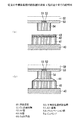
ここで、図7及び図8を参照して従来の半導体集積回路装置の実装工程を説明する。
まず、図7(a)に示すように、回路基板40の表面に設けたCu表面電極41の表面にCuと液相拡散するSn層42と、液相拡散温度を下げるBi層43を順次堆積する。一方、Cuバンプ54を設けた半導体集積回路装置50を、ボンディングツールを例えば、150℃に加熱した状態でCuバンプ54とCu表面電極41とが当接するように押圧する。なお、図における符号51,52は電極層であり、53はパッシベーション膜である。
Here, a conventional semiconductor integrated circuit device mounting process will be described with reference to FIGS.
First, as shown in FIG. 7A, an
この時、図7(b)に示すように、Bi層43とSn層42は、150℃に加熱されたCuバンプ54と当接することによって溶融してSnBi共晶44を形成し、室温まで降温することによって接合が形成される。
At this time, as shown in FIG. 7B, the
次いで、図8(c)に示すように、接合形成後に、リフローやアンダーフィル硬化のためのアニール等で150℃を超える、例えば、180℃程度の熱が加わると、Cuバンプ54或いはCu表面電極41とSnBi共晶44中のSnが反応してCuSn金属間化合物45を形成する。これは、BiはSnと比較してCuとの反応性が低いため、SnがCu中に液相拡散していくためである。
Next, as shown in FIG. 8 (c), after bonding, when heat exceeding 150 ° C., for example, about 180 ° C. is applied by annealing for reflow or underfill curing, the
ついで、図8(d)に示すように、室温まで降温して固化させると、接合界面においては、CuSn金属間化合物45の間にBi単体46が残存した状態となる。
上述のように、SnとBiの共晶反応を利用した接合方法においては、溶融接合後にリフローやアニールなどで熱が加わると接合界面にBi単体が取り残される。このBi単体は非常に脆いため、このBi単体を起点にクラックが生じやすくなり接合信頼性を大幅に低下させるという問題があった. As described above, in the bonding method using the eutectic reaction of Sn and Bi, when heat is applied by reflow or annealing after melt bonding, Bi alone is left behind at the bonding interface. Since this Bi alone is very fragile, there is a problem that cracks are likely to occur starting from this Bi alone and the joint reliability is greatly reduced.
したがって、本発明は、接合界面におけるBi濃度を低減して接合信頼性を高めることを目的とする。 Accordingly, an object of the present invention is to increase the reliability of bonding by reducing the Bi concentration at the bonding interface.
本発明の一観点からは、電極を表面に備えた配線基板と、前記電極に対向するバンプを表面に備えた電子部品とを有し、前記電極と前記バンプとの間の領域にSn及びBiを含む接合層が形成され、前記接合層における第1の領域のBi含有率が、前記接合層における第2の領域のBi含有率よりも低い回路基板が提供される。 From one aspect of the present invention, a wiring board having electrodes on its surface and an electronic component having bumps on its surface facing the electrodes are provided, and Sn and Bi are provided in a region between the electrodes and the bumps. And a circuit board is provided in which the Bi content of the first region in the bonding layer is lower than the Bi content of the second region in the bonding layer.
また、本発明の別の観点からは、配線基板の表面に設けた電極上にSnを含む第1の層とBiを含む第2の層を形成する工程と、電子部品の表面に設けた前記電極に対向するバンプ上にSn含有金属層を形成する工程と、前記バンプを加熱する工程と、前記加熱の後に或いは前記加熱しながら、前記バンプを前記電極に押し付けて、前記電極と前記バンプを接合する工程とを有する回路基板の製造方法が提供される。 From another viewpoint of the present invention, a step of forming a first layer containing Sn and a second layer containing Bi on an electrode provided on the surface of the wiring board; Forming a Sn-containing metal layer on the bump facing the electrode; heating the bump; pressing the bump against the electrode after or while heating; There is provided a method of manufacturing a circuit board having a bonding step.
開示の回路基板によれば、SnBi共晶におけるBiを周辺部に押し出して、接合界面におけるBi濃度を低減しているので、Biの欠点である脆性による影響を排除した確実な電気的接点を形成することができる。 According to the disclosed circuit board, Bi in the SnBi eutectic is extruded to the peripheral part to reduce the Bi concentration at the bonding interface, thereby forming a reliable electrical contact that eliminates the influence of brittleness, which is a disadvantage of Bi. can do.
ここで、図1を参照して、本発明の実施の形態を説明する。図1は、本発明の実施の形態のフローチャートであり、まず、
A.コンタクト前の工程として、回路基板の表面に設けたCuまたはAg、或いは、これらを主成分とする合金からなる表面電極の上に、CuやAgに対して液相拡散しやすいSn層及び液相温度を下げるためのBi層を電解めっき法或いは無電解めっき法によって順次堆積させる。この時、Sn層及びBi層は重量比で1:1になるように膜厚を制御する。なお、Sn層とBi層の積層順序は反対でも良く、或いは、SnとBiとの重量比が1:1のSnBi合金ペーストを印刷法によって形成しても良い。
Here, an embodiment of the present invention will be described with reference to FIG. FIG. 1 is a flowchart of an embodiment of the present invention.
A. As a pre-contact process, an Sn layer and a liquid phase that are liable to liquid phase diffuse with respect to Cu or Ag on Cu or Ag provided on the surface of the circuit board or a surface electrode made of an alloy containing these as a main component. Bi layers for lowering the temperature are sequentially deposited by electrolytic plating or electroless plating. At this time, the film thickness is controlled so that the Sn layer and the Bi layer have a weight ratio of 1: 1. The order of stacking the Sn layer and Bi layer may be reversed, or an SnBi alloy paste having a 1: 1 weight ratio of Sn to Bi may be formed by a printing method.
一方、半導体集積回路装置に設けたCu、Au等からなるバンプの表面にSn層を電解めっき法、無電解めっき法、或いは、マスクスパッタ法等により形成する。なお、電解めっき法でSn層を形成する場合には、メッキシード層とレジストフレームを用いて電解めっきを行い、Sn層を形成したのち、メッキシード層とレジストフレームを除去する。 On the other hand, an Sn layer is formed on the surface of a bump made of Cu, Au or the like provided in the semiconductor integrated circuit device by an electrolytic plating method, an electroless plating method, a mask sputtering method, or the like. In the case of forming the Sn layer by electrolytic plating, electrolytic plating is performed using a plating seed layer and a resist frame to form the Sn layer, and then the plating seed layer and the resist frame are removed.
次いで、蟻酸雰囲気中で加熱してリフローを行うことによって、Sn層を溶融して半球状Sn層に成形する。この場合、蟻酸は還元性が強いので、熱処理によりSnが酸化されることはない。なお、このようなリフロー工程は、フラックスを用いてN2 雰囲気下で行っても良いし、或いは、真空下でリフローしても良い。 Next, the Sn layer is melted and formed into a hemispherical Sn layer by performing reflow by heating in a formic acid atmosphere. In this case, since formic acid is highly reducible, Sn is not oxidized by the heat treatment. Such a reflow process may be performed under N 2 atmosphere using a flux, or may be reflowed under vacuum.
次いで、
B.フリップチップ接合の第1段階として、回路基板を搭載するステージの温度をSnとBiとの共晶形成温度より低い温度まで昇温した状態で、ボンディングツールに保持した半導体集積回路装置を、パッドと表面電極が当接するように押圧した状態で、ボンディングツールをSnとBiとの共晶形成温度より高温に昇温する。なお、半球状Sn層のSnの酸化膜除去のためにフラックスを予め塗布しておくか、またはフラックス機能を有するアンダーフィルと同時に接合する。或いは、接合前にArプラズマ、水素プラズマによって酸化膜を除去しておくことも可能である。
Then
B. As a first stage of flip chip bonding, a semiconductor integrated circuit device held in a bonding tool in a state where the temperature of a stage on which a circuit board is mounted is raised to a temperature lower than the eutectic formation temperature of Sn and Bi, The temperature of the bonding tool is raised to a temperature higher than the eutectic formation temperature of Sn and Bi with the surface electrode pressed so as to come into contact. In addition, in order to remove the Sn oxide film of the hemispherical Sn layer, a flux is applied in advance or it is joined simultaneously with an underfill having a flux function. Alternatively, the oxide film can be removed by Ar plasma or hydrogen plasma before bonding.
この時、Bi層とSn層は、当接した半球状Sn層がSnとBiとの共晶形成温度より高温に昇温することにより溶融してSnBi共晶を形成する。この溶融したSnBi共晶は、固相(Snの融点:232℃)のままである半球状Sn層が押し付けられることによって、周囲に押し出される。 At this time, the Bi layer and the Sn layer are melted when the abutting hemispherical Sn layer is heated to a temperature higher than the eutectic formation temperature of Sn and Bi to form a SnBi eutectic. The melted SnBi eutectic is pushed out by pressing the hemispherical Sn layer that remains in the solid phase (Sn melting point: 232 ° C.).
次いで、
C.フリップチップ接合の第2段階として、半球状Sn層の最表層は溶融したSnBi共晶へ溶け出すため、この部分で金属接合が生じ、半導体集積回路装置と回路基板の電極同士が電気的に接続されることになる。
Then
C. As the second stage of flip chip bonding, the outermost layer of the hemispherical Sn layer melts into the molten SnBi eutectic, so that metal bonding occurs at this part, and the semiconductor integrated circuit device and the circuit board electrodes are electrically connected to each other Will be.
次いで、
D.フリップチップ接合の第3段階として、加圧した状態でボンディングツールをSnとBiとの共晶形成温度より低い温度まで降温して溶融したSnBi共晶を固化して固相SnBi共晶とする。この時、接合界面にBi単体が一部取り残されるが、従来に比べて非常に低濃度になる。
Then
D. As a third stage of the flip chip bonding, the SnBi eutectic melted by lowering the temperature of the bonding tool to a temperature lower than the eutectic formation temperature of Sn and Bi in a pressurized state is solidified into a solid-phase SnBi eutectic. At this time, a part of Bi is left behind at the bonding interface, but the concentration is very low compared to the conventional case.
次いで、
E.ポストアニール工程として、例えば、アンダーフィル樹脂を硬化するため熱処理を行う。この時の熱処理温度は、接合工程における温度より高温であるので、固相SnBi共晶が再び溶融し、SnがCuへ液相拡散して高融点金属のCuSn金属間化合物層を形成する。
Then
E. As the post-annealing step, for example, heat treatment is performed to cure the underfill resin. Since the heat treatment temperature at this time is higher than the temperature in the bonding step, the solid-phase SnBi eutectic is melted again, and Sn is liquid phase diffused into Cu to form a CuSn intermetallic compound layer of a refractory metal.
また、溶融したSnBi共晶中のSnが拡散してCuと反応することにより、溶融したSnBi共晶中のBi濃度が高まり、最後には、Bi比率の非常に高いBi層がCuSn金属間化合物層の表面を覆うことになる。 Further, Sn in the melted SnBi eutectic diffuses and reacts with Cu, so that the Bi concentration in the melted SnBi eutectic increases, and finally, a Bi layer having a very high Bi ratio becomes a CuSn intermetallic compound. It will cover the surface of the layer.
なお、工程Eのポストアニール工程において、CuSn金属間化合物層を形成するアニール工程を兼ねて行っているが、ポストアニール工程の前に、上記の工程Cのフリップチップ接合の第2段階の直後に行うようにしても良い。 In the post-annealing process of process E, the annealing process for forming the CuSn intermetallic compound layer is also performed, but immediately after the second stage of the flip-chip bonding in the above-mentioned process C before the post-annealing process. You may make it do.
このように、本発明の実施の形態においては、SnBi共晶を利用して接合する際に、半導体集積回路装置側のバンプの表面に半球状Sn層を設けているので、接合界面近傍のBi濃度が低減し、さらに、ポストアニールで高融点金属のCuSn金属間化合物層を形成しているので、熱的に安定な接合を形成することができる。 As described above, in the embodiment of the present invention, when bonding using SnBi eutectic, the hemispherical Sn layer is provided on the surface of the bump on the semiconductor integrated circuit device side. Since the concentration is reduced and the CuSn intermetallic compound layer of a refractory metal is formed by post-annealing, a thermally stable bond can be formed.
以上を前提として、次に、図2乃至図6を参照して、本発明の実施例1のフリップチップ接合工程を説明する。まず、図2(a)に示すように、回路基板(図示は省略)の表面に設けた例えば、Cuからなる表面電極12の上に、Sn層13及びBi層14を電解めっき法によって順次堆積させる。この時、Sn層13及びBi層14は重量比で1:1になるように膜厚を各1μmにする。
Based on the above, next, the flip chip bonding process of the first embodiment of the present invention will be described with reference to FIGS. First, as shown in FIG. 2A, an
一方、図2(b)に示すように、半導体集積回路装置(図示は省略)に電解めっき法を用いて、厚さが、例えば、12μmのCuからなるバンプ24及び厚さが、例えば、3μmのSn層25を順次形成する。この場合、メッキシード層とレジストフレーム(いずれも図示を省略)を用いて電解めっきを行い、バンプ24及びSn層25を形成したのち、メッキシード層とレジストフレームを除去する。
On the other hand, as shown in FIG. 2B, a
次いで、図2(c)に示すように、ウェハ用フラックスレスリフロー装置(アユミ工業社製)を用いて、蟻酸雰囲気中で、例えば、245℃に加熱してリフローを行うことによって、Sn層25を溶融して半球状Sn層26に成形する。
Next, as shown in FIG. 2 (c), by using a wafer fluxless reflow apparatus (manufactured by Ayumi Kogyo Co., Ltd.) and performing reflow by heating to 245 ° C. in a formic acid atmosphere, the
次いで、これらの半導体集積回路装置と回路基板とをフリップチップボンダーによって位置合わせし、フリップチップ接合を行う。まず、図2(d)に示すように、回路基板を搭載するステージの温度をSnとBiとの共晶形成温度より低い135℃まで昇温した状態で、パッド24と表面電極12が当接するように押圧しながら、半導体集積回路装置を吸着したボンディングツールの温度を50℃からSnとBiとの共晶形成温度より高い150℃まで、例えば、1秒で昇温する。この時の押圧力は、100〜200Paであり、1バンプ当たりにすると、例えば、5gfの力を加える。
Next, the semiconductor integrated circuit device and the circuit board are aligned by a flip chip bonder to perform flip chip bonding. First, as shown in FIG. 2D, the
次いで、図2(e)に示すように、Bi層13とSn層14は、SnとBiとの共晶形成温度より高い150℃に加熱された半球状Sn26が当接することにより溶融してSnBi共晶15を形成する。この溶融したSnBi共晶15は、固相(Snの融点:232℃)のままである半球状Sn層26が押し付けられることによって、徐々に周囲に押し出される。
Next, as shown in FIG. 2 (e), the
この時、図3(f)に示すように、半球状Sn層26の最表層は溶融したSnBi共晶15へ溶け出すため、この部分で金属接合が生じ、半導体集積回路装置と回路基板の電極同士が電気的に接続されることになる。表面の溶出により半球状半田26はSn層27となる。
At this time, as shown in FIG. 3 (f), the outermost layer of the
次いで、例えば、150℃に昇温してから9秒経過したのち、図3(g)に示すように、加圧した状態でボンディングツールをSnとBiとの共晶形成温度より低い温度まで降温して溶融したSnBi共晶15を固化して固相SnBi共晶16とする。この時、接合界面にBi単体17が一部取り残されるが、従来に比べて非常に低濃度になる。次いで、ボンディングツールの温度が例えば、5秒間で100℃まで降温した時に、押圧を解除して、以降は室温まで自然冷却する。
Next, for example, after 9 seconds have passed since the temperature was raised to 150 ° C., the temperature of the bonding tool was lowered to a temperature lower than the eutectic formation temperature of Sn and Bi as shown in FIG. The melted
次いで、図3(h)に示すように、ポストアニール工程として、例えば、アンダーフィル樹脂を硬化するため熱処理を行う。この時の熱処理温度は、接合工程における温度より高温、例えば、165℃で1.5時間の熱処理工程であるので、固相SnBi共晶16が再び溶融するとともに、Sn層27からSnがCuへ液相拡散して高融点金属のCuSn金属間化合物層18を形成する。また、溶融したSnBi共晶中のSnが拡散してCuと反応することにより、溶融したSnBi共晶中のBi濃度が高まり、最後には、Bi比率の非常に高いBi層19がCu6 Sn5 からなるCuSn金属間化合物層18の表面を覆うことになる。
Next, as shown in FIG. 3H, as the post-annealing step, for example, heat treatment is performed to cure the underfill resin. Since the heat treatment temperature at this time is a heat treatment step higher than the temperature in the bonding step, for example, 165 ° C. for 1.5 hours, the solid-
図4は、本発明の実施例1の半導体実装装置の概念的構成図であり、上述の方法で形成された接合部を有するとともに、半導体集積回路装置20と回路基板10との間にアンダーフィル樹脂28が充填されるとともに、エポキシ樹脂29でモールドされた半導体実装装置が得られる。なお、図における符号21,22,23,11,30,31は、それぞれ半導体基体、電極、パッシベーション膜、ベース層、ソルダーレジスト及び半田ボールを表す。
FIG. 4 is a conceptual configuration diagram of the semiconductor mounting apparatus according to the first embodiment of the present invention. The semiconductor mounting apparatus includes a joint formed by the above-described method and an underfill between the semiconductor integrated
図5は、上記の本発明の実施例1のフリップチップ接合工程における各条件を纏めた図であり、また、図6は、本発明の実施例1のフリップチップ接合工程における各条件をグラフ化したプロファイルである。 FIG. 5 is a diagram summarizing the conditions in the flip-chip bonding process of the first embodiment of the present invention, and FIG. 6 is a graph showing the conditions in the flip-chip bonding process of the first embodiment of the present invention. Profile.
以上、本発明の実施の形態及び実施例を説明してきたが、上記の実施の形態及び実施例に示した構成は一例であり、各種の変更が可能である。例えば、上記の実施例1においては、実装する側を回路基板としているが、回路基板に限られるものではなく、所定の配線を形成したパッケージ基板でも良い。 Although the embodiments and examples of the present invention have been described above, the configurations shown in the above embodiments and examples are merely examples, and various modifications can be made. For example, in the first embodiment, the circuit board is used as the mounting side. However, the circuit board is not limited to the circuit board, and a package board on which predetermined wiring is formed may be used.
また、上記の実施例1においては、実装される部品を半導体集積回路装置としているが、半導体集積回路装置に限られるものではなく、例えば、強誘電体を用いた光偏向装置等の光デバイスの実装にも用いられるものである。 In the first embodiment, the component to be mounted is a semiconductor integrated circuit device. However, the component is not limited to the semiconductor integrated circuit device. For example, an optical device such as an optical deflection device using a ferroelectric is used. It is also used for implementation.
ここで、実施例1を含む本発明の実施の形態に関して、以下の付記を開示する。
(付記1) 電極を表面に備えた配線基板と、
前記電極に対向するバンプを表面に備えた電子部品と
を有し、
前記電極と前記バンプとの間の領域にSn及びBiを含む接合層が形成され、前記接合層における第1の領域のBi含有率が、前記接合層における第2の領域のBi含有率よりも低い回路基板。
(付記2) 前記第1の領域は、前記バンプと前記電極によって挟まれた領域である付記1記載の回路基板。
(付記3) 前記電極及び前記バンプは、前記Snの融点よりも高い融点を有する金属である付記1または2に記載の回路基板。
(付記4) 配線基板の表面に設けた電極上にSnを含む第1の層とBiを含む第2の層を形成する工程と、
電子部品の表面に設けた前記電極に対向するバンプ上にSn含有金属層を形成する工程と、
前記バンプを加熱する工程と、
前記加熱の後に或いは前記加熱しながら、前記バンプを前記電極に押し付けて、前記電極と前記バンプを接合する工程と
を有する回路基板の製造方法。
(付記5) 前記Snを含む第1の層と前記Biを含む第2の層の重量比が1:1である付記4記載の回路基板の製造方法。
(付記6) 前記加熱する温度は、SnとBiの共晶温度以上且つ前記Sn含有金属層の融点未満の温度である付記4または5に記載の回路基板の製造方法。
(付記7) 前記Sn含有金属層の形状が半球状である付記4乃至6のいずれか1に記載の記載の回路基板の製造方法。
(付記8) 前記加熱の前に、前記第1の層及び前記第2の層を前記Snと前記Biの共晶温度より低い温度で予備加熱する工程をさらに有する付記4乃至7のいずれか1に記載の回路基板の製造方法。
Here, regarding the embodiment of the present invention including Example 1, the following additional notes are disclosed.
(Supplementary note 1) a wiring board having electrodes on its surface;
An electronic component provided with bumps facing the electrodes on the surface;
A bonding layer containing Sn and Bi is formed in a region between the electrode and the bump, and the Bi content of the first region in the bonding layer is higher than the Bi content of the second region in the bonding layer. Low circuit board.
(Supplementary note 2) The circuit board according to supplementary note 1, wherein the first region is a region sandwiched between the bump and the electrode.
(Additional remark 3) The said electrode and the said bump are the circuit boards of
(Additional remark 4) The process of forming the 1st layer containing Sn and the 2nd layer containing Bi on the electrode provided in the surface of the wiring board,
Forming a Sn-containing metal layer on a bump facing the electrode provided on the surface of the electronic component;
Heating the bump;
A method of manufacturing a circuit board, comprising the step of pressing the bump against the electrode after the heating or while heating, and bonding the electrode and the bump.
(Additional remark 5) The manufacturing method of the circuit board of
(Supplementary note 6) The circuit board manufacturing method according to
(Additional remark 7) The manufacturing method of the circuit board of any one of
(Supplementary note 8) Any one of
10 回路基板
11 ベース層
12 表面電極
13 Sn層
14 Bi層
15 SnBi共晶
16 固相SnBi共晶
17 Bi単体
18 CuSn金属間化合物層
19 Bi層
20 半導体集積回路装置
21 半導体基体
22 電極
23 パッシベーション膜
24 バンプ
25 Sn層
26 半球状Sn層
27 Sn層
28 アンダーフィル樹脂
29 エポキシ樹脂
30 ソルダーレジスト
31 半田ボール
40 回路基板
41 Cu表面電極
42 Sn層
43 Bi層
44 SnBi共晶
45 CuSn金属間化合物
46 Bi単体
50 半導体集積回路装置
51,52 電極層
53 パッシベーション膜
54 Cuバンプ
DESCRIPTION OF
Claims (5)
前記電極に対向するバンプを表面に備えた電子部品と
を有し、
前記電極と前記バンプとの間の領域にSn及びBiを含む接合層が形成され、前記接合層における第1の領域のBi含有率が、前記接合層における第2の領域のBi含有率よりも低い回路基板。 A wiring board with electrodes on the surface;
An electronic component provided with bumps facing the electrodes on the surface;
A bonding layer containing Sn and Bi is formed in a region between the electrode and the bump, and the Bi content of the first region in the bonding layer is higher than the Bi content of the second region in the bonding layer. Low circuit board.
電子部品の表面に設けた前記電極に対向するバンプ上にSn含有金属層を形成する工程と、
前記バンプを加熱する工程と、
前記加熱の後に或いは前記加熱しながら、前記バンプを前記電極に押し付けて、前記電極と前記バンプを接合する工程と
を有する回路基板の製造方法。 Forming a first layer containing Sn and a second layer containing Bi on an electrode provided on the surface of the wiring board;
Forming a Sn-containing metal layer on a bump facing the electrode provided on the surface of the electronic component;
Heating the bump;
A method of manufacturing a circuit board, comprising the step of pressing the bump against the electrode after the heating or while heating, and bonding the electrode and the bump.
Priority Applications (1)
| Application Number | Priority Date | Filing Date | Title |
|---|---|---|---|
| JP2008161409A JP5035134B2 (en) | 2008-06-20 | 2008-06-20 | Electronic component mounting apparatus and manufacturing method thereof |
Applications Claiming Priority (1)
| Application Number | Priority Date | Filing Date | Title |
|---|---|---|---|
| JP2008161409A JP5035134B2 (en) | 2008-06-20 | 2008-06-20 | Electronic component mounting apparatus and manufacturing method thereof |
Publications (2)
| Publication Number | Publication Date |
|---|---|
| JP2010003878A true JP2010003878A (en) | 2010-01-07 |
| JP5035134B2 JP5035134B2 (en) | 2012-09-26 |
Family
ID=41585352
Family Applications (1)
| Application Number | Title | Priority Date | Filing Date |
|---|---|---|---|
| JP2008161409A Expired - Fee Related JP5035134B2 (en) | 2008-06-20 | 2008-06-20 | Electronic component mounting apparatus and manufacturing method thereof |
Country Status (1)
| Country | Link |
|---|---|
| JP (1) | JP5035134B2 (en) |
Cited By (7)
| Publication number | Priority date | Publication date | Assignee | Title |
|---|---|---|---|---|
| JP2011216813A (en) * | 2010-04-02 | 2011-10-27 | Fujitsu Ltd | Solder joint method, semiconductor device and method of manufacturing the same |
| JP2012227438A (en) * | 2011-04-21 | 2012-11-15 | Panasonic Corp | Semiconductor device manufacturing method and semiconductor device |
| JP2013093547A (en) * | 2011-10-05 | 2013-05-16 | Fujitsu Ltd | Semiconductor device, electronic apparatus and semiconductor device manufacturing method |
| JP2015072996A (en) * | 2013-10-02 | 2015-04-16 | 新光電気工業株式会社 | Semiconductor device |
| JP2017175044A (en) * | 2016-03-25 | 2017-09-28 | 富士通株式会社 | Wiring board, manufacturing method of wiring board, and electronic device |
| US11088308B2 (en) | 2019-02-25 | 2021-08-10 | Tdk Corporation | Junction structure |
| EP4090141A1 (en) | 2021-05-10 | 2022-11-16 | Shinko Electric Industries Co., Ltd. | Composite wiring substrate, semiconductor device, and method of manufacturing composite wiring substrate |
Citations (4)
| Publication number | Priority date | Publication date | Assignee | Title |
|---|---|---|---|---|
| JPH0831835A (en) * | 1994-07-20 | 1996-02-02 | Fujitsu Ltd | Semiconductor device, electronic circuit device, and production thereof |
| JPH1174415A (en) * | 1997-06-23 | 1999-03-16 | Ford Motor Co | Method for forming interconnection of electronic module |
| JP2007324447A (en) * | 2006-06-02 | 2007-12-13 | Hitachi Kyowa Engineering Co Ltd | Electronic component mounting substrate, and electronic component and device |
| JP2008109009A (en) * | 2006-10-27 | 2008-05-08 | Sony Corp | Method of manufacturing semiconductor device |
-
2008
- 2008-06-20 JP JP2008161409A patent/JP5035134B2/en not_active Expired - Fee Related
Patent Citations (4)
| Publication number | Priority date | Publication date | Assignee | Title |
|---|---|---|---|---|
| JPH0831835A (en) * | 1994-07-20 | 1996-02-02 | Fujitsu Ltd | Semiconductor device, electronic circuit device, and production thereof |
| JPH1174415A (en) * | 1997-06-23 | 1999-03-16 | Ford Motor Co | Method for forming interconnection of electronic module |
| JP2007324447A (en) * | 2006-06-02 | 2007-12-13 | Hitachi Kyowa Engineering Co Ltd | Electronic component mounting substrate, and electronic component and device |
| JP2008109009A (en) * | 2006-10-27 | 2008-05-08 | Sony Corp | Method of manufacturing semiconductor device |
Cited By (9)
| Publication number | Priority date | Publication date | Assignee | Title |
|---|---|---|---|---|
| JP2011216813A (en) * | 2010-04-02 | 2011-10-27 | Fujitsu Ltd | Solder joint method, semiconductor device and method of manufacturing the same |
| JP2012227438A (en) * | 2011-04-21 | 2012-11-15 | Panasonic Corp | Semiconductor device manufacturing method and semiconductor device |
| JP2013093547A (en) * | 2011-10-05 | 2013-05-16 | Fujitsu Ltd | Semiconductor device, electronic apparatus and semiconductor device manufacturing method |
| JP2015072996A (en) * | 2013-10-02 | 2015-04-16 | 新光電気工業株式会社 | Semiconductor device |
| JP2017175044A (en) * | 2016-03-25 | 2017-09-28 | 富士通株式会社 | Wiring board, manufacturing method of wiring board, and electronic device |
| US11088308B2 (en) | 2019-02-25 | 2021-08-10 | Tdk Corporation | Junction structure |
| EP4090141A1 (en) | 2021-05-10 | 2022-11-16 | Shinko Electric Industries Co., Ltd. | Composite wiring substrate, semiconductor device, and method of manufacturing composite wiring substrate |
| KR20220152937A (en) | 2021-05-10 | 2022-11-17 | 신꼬오덴기 고교 가부시키가이샤 | Composite wiring substrate, semiconductor device and method of manufacturing composite wiring substrate |
| US11706877B2 (en) | 2021-05-10 | 2023-07-18 | Shinko Electric Industries Co., Ltd. | Composite wiring substrate and semiconductor device |
Also Published As
| Publication number | Publication date |
|---|---|
| JP5035134B2 (en) | 2012-09-26 |
Similar Documents
| Publication | Publication Date | Title |
|---|---|---|
| KR100719905B1 (en) | Sn-bi alloy solder and semiconductor using the same | |
| JP5378078B2 (en) | Manufacturing method of semiconductor device | |
| JP5035134B2 (en) | Electronic component mounting apparatus and manufacturing method thereof | |
| US7534715B2 (en) | Methods including fluxless chip attach processes | |
| US8409919B2 (en) | Method for manufacturing semiconductor device | |
| TW200829361A (en) | Connecting material, method for manufacturing connecting material, and semiconductor device | |
| TWI414049B (en) | Semiconductor device manufacturing method | |
| KR102121176B1 (en) | Method for producing semiconductor package | |
| JP2009060101A (en) | Electronic device | |
| CN103123916B (en) | Semiconductor device, electronic device and method, semi-conductor device manufacturing method | |
| JP2007287712A (en) | Semiconductor device, packaging structure thereof, and manufacturing method of semiconductor device and packaging structure | |
| JP4961165B2 (en) | Electronic component mounting substrate, electronic component and electronic device | |
| JP2007059485A (en) | Semiconductor device, substrate and method of manufacturing semiconductor device | |
| US8701281B2 (en) | Substrate metallization and ball attach metallurgy with a novel dopant element | |
| JP6398499B2 (en) | Electronic device and method of manufacturing electronic device | |
| JP2015115363A (en) | Electronic device and method of manufacturing electronic device | |
| TWI723424B (en) | Manufacturing method of semiconductor device | |
| Baggerman et al. | Reliable Au-Sn flip-chip bonding on flexible prints | |
| WO2011030517A1 (en) | Connecting material, semiconductor device and method for manufacturing semiconductor device | |
| JP4175858B2 (en) | Method for producing solder-coated balls | |
| KR102181706B1 (en) | Method for producing semiconductor chip | |
| JP5401996B2 (en) | Manufacturing method of semiconductor device | |
| JP2012129482A (en) | Method for manufacturing semiconductor device | |
| JP2009194357A (en) | Semiconductor device and method of manufacturing the same | |
| JP2008071792A (en) | Method of manufacturing semiconductor device |
Legal Events
| Date | Code | Title | Description |
|---|---|---|---|
| A621 | Written request for application examination |
Free format text: JAPANESE INTERMEDIATE CODE: A621 Effective date: 20110315 |
|
| RD03 | Notification of appointment of power of attorney |
Free format text: JAPANESE INTERMEDIATE CODE: A7423 Effective date: 20110915 |
|
| A977 | Report on retrieval |
Free format text: JAPANESE INTERMEDIATE CODE: A971007 Effective date: 20120319 |
|
| A131 | Notification of reasons for refusal |
Free format text: JAPANESE INTERMEDIATE CODE: A131 Effective date: 20120327 |
|
| A521 | Written amendment |
Free format text: JAPANESE INTERMEDIATE CODE: A523 Effective date: 20120521 |
|
| TRDD | Decision of grant or rejection written | ||
| A01 | Written decision to grant a patent or to grant a registration (utility model) |
Free format text: JAPANESE INTERMEDIATE CODE: A01 Effective date: 20120605 |
|
| A01 | Written decision to grant a patent or to grant a registration (utility model) |
Free format text: JAPANESE INTERMEDIATE CODE: A01 |
|
| A61 | First payment of annual fees (during grant procedure) |
Free format text: JAPANESE INTERMEDIATE CODE: A61 Effective date: 20120618 |
|
| FPAY | Renewal fee payment (event date is renewal date of database) |
Free format text: PAYMENT UNTIL: 20150713 Year of fee payment: 3 |
|
| R150 | Certificate of patent or registration of utility model |
Free format text: JAPANESE INTERMEDIATE CODE: R150 |
|
| LAPS | Cancellation because of no payment of annual fees |