JP2010002926A - 光偏向器の製造方法 - Google Patents
光偏向器の製造方法 Download PDFInfo
- Publication number
- JP2010002926A JP2010002926A JP2009223313A JP2009223313A JP2010002926A JP 2010002926 A JP2010002926 A JP 2010002926A JP 2009223313 A JP2009223313 A JP 2009223313A JP 2009223313 A JP2009223313 A JP 2009223313A JP 2010002926 A JP2010002926 A JP 2010002926A
- Authority
- JP
- Japan
- Prior art keywords
- movable plate
- optical deflector
- drive coil
- support
- magnetic
- Prior art date
- Legal status (The legal status is an assumption and is not a legal conclusion. Google has not performed a legal analysis and makes no representation as to the accuracy of the status listed.)
- Granted
Links
- 230000003287 optical effect Effects 0.000 title claims abstract description 143
- 238000004519 manufacturing process Methods 0.000 title claims description 27
- 230000005489 elastic deformation Effects 0.000 claims description 6
- 239000004642 Polyimide Substances 0.000 description 57
- 229920001721 polyimide Polymers 0.000 description 57
- 230000004907 flux Effects 0.000 description 27
- 239000000758 substrate Substances 0.000 description 27
- XUIMIQQOPSSXEZ-UHFFFAOYSA-N Silicon Chemical compound [Si] XUIMIQQOPSSXEZ-UHFFFAOYSA-N 0.000 description 25
- 229910052710 silicon Inorganic materials 0.000 description 25
- 239000010703 silicon Substances 0.000 description 25
- 239000010408 film Substances 0.000 description 23
- 238000000034 method Methods 0.000 description 17
- 229910052581 Si3N4 Inorganic materials 0.000 description 10
- HQVNEWCFYHHQES-UHFFFAOYSA-N silicon nitride Chemical compound N12[Si]34N5[Si]62N3[Si]51N64 HQVNEWCFYHHQES-UHFFFAOYSA-N 0.000 description 10
- 238000005530 etching Methods 0.000 description 9
- 230000004048 modification Effects 0.000 description 9
- 238000012986 modification Methods 0.000 description 9
- 229910052782 aluminium Inorganic materials 0.000 description 8
- XAGFODPZIPBFFR-UHFFFAOYSA-N aluminium Chemical compound [Al] XAGFODPZIPBFFR-UHFFFAOYSA-N 0.000 description 8
- 230000005415 magnetization Effects 0.000 description 8
- 239000000463 material Substances 0.000 description 8
- 230000008569 process Effects 0.000 description 6
- 230000000694 effects Effects 0.000 description 5
- 230000005484 gravity Effects 0.000 description 5
- 238000004544 sputter deposition Methods 0.000 description 5
- 238000001312 dry etching Methods 0.000 description 4
- 239000011810 insulating material Substances 0.000 description 4
- 238000000059 patterning Methods 0.000 description 4
- 238000007639 printing Methods 0.000 description 4
- 238000006073 displacement reaction Methods 0.000 description 3
- 238000001035 drying Methods 0.000 description 3
- 239000007788 liquid Substances 0.000 description 3
- 230000007935 neutral effect Effects 0.000 description 3
- 239000004065 semiconductor Substances 0.000 description 3
- 239000000243 solution Substances 0.000 description 3
- 239000010409 thin film Substances 0.000 description 3
- 239000000853 adhesive Substances 0.000 description 2
- 230000001070 adhesive effect Effects 0.000 description 2
- 230000008859 change Effects 0.000 description 2
- 239000012787 coverlay film Substances 0.000 description 2
- 239000013078 crystal Substances 0.000 description 2
- 238000000151 deposition Methods 0.000 description 2
- 238000005516 engineering process Methods 0.000 description 2
- 230000003993 interaction Effects 0.000 description 2
- 230000001678 irradiating effect Effects 0.000 description 2
- 210000003041 ligament Anatomy 0.000 description 2
- 230000007246 mechanism Effects 0.000 description 2
- 229910052751 metal Inorganic materials 0.000 description 2
- 239000002184 metal Substances 0.000 description 2
- 238000005459 micromachining Methods 0.000 description 2
- 150000004767 nitrides Chemical class 0.000 description 2
- 238000007747 plating Methods 0.000 description 2
- 238000004528 spin coating Methods 0.000 description 2
- 238000007738 vacuum evaporation Methods 0.000 description 2
- VYZAMTAEIAYCRO-UHFFFAOYSA-N Chromium Chemical compound [Cr] VYZAMTAEIAYCRO-UHFFFAOYSA-N 0.000 description 1
- RYGMFSIKBFXOCR-UHFFFAOYSA-N Copper Chemical compound [Cu] RYGMFSIKBFXOCR-UHFFFAOYSA-N 0.000 description 1
- 229910017116 Fe—Mo Inorganic materials 0.000 description 1
- 229910003271 Ni-Fe Inorganic materials 0.000 description 1
- 239000012670 alkaline solution Substances 0.000 description 1
- 229910045601 alloy Inorganic materials 0.000 description 1
- 239000000956 alloy Substances 0.000 description 1
- 238000013459 approach Methods 0.000 description 1
- QVGXLLKOCUKJST-UHFFFAOYSA-N atomic oxygen Chemical compound [O] QVGXLLKOCUKJST-UHFFFAOYSA-N 0.000 description 1
- 238000005452 bending Methods 0.000 description 1
- 229910052804 chromium Inorganic materials 0.000 description 1
- 239000011651 chromium Substances 0.000 description 1
- 229910052802 copper Inorganic materials 0.000 description 1
- 239000010949 copper Substances 0.000 description 1
- 230000007423 decrease Effects 0.000 description 1
- 238000010586 diagram Methods 0.000 description 1
- 230000005284 excitation Effects 0.000 description 1
- PCHJSUWPFVWCPO-UHFFFAOYSA-N gold Chemical compound [Au] PCHJSUWPFVWCPO-UHFFFAOYSA-N 0.000 description 1
- 239000010931 gold Substances 0.000 description 1
- 229910052737 gold Inorganic materials 0.000 description 1
- 238000009413 insulation Methods 0.000 description 1
- 238000010030 laminating Methods 0.000 description 1
- 238000000608 laser ablation Methods 0.000 description 1
- 230000007774 longterm Effects 0.000 description 1
- 238000004518 low pressure chemical vapour deposition Methods 0.000 description 1
- 229910052759 nickel Inorganic materials 0.000 description 1
- 239000011368 organic material Substances 0.000 description 1
- 230000003647 oxidation Effects 0.000 description 1
- 238000007254 oxidation reaction Methods 0.000 description 1
- 229910052760 oxygen Inorganic materials 0.000 description 1
- 239000001301 oxygen Substances 0.000 description 1
- 230000002093 peripheral effect Effects 0.000 description 1
- 229910000889 permalloy Inorganic materials 0.000 description 1
- 238000000206 photolithography Methods 0.000 description 1
- 230000000704 physical effect Effects 0.000 description 1
- 238000005498 polishing Methods 0.000 description 1
- 238000002310 reflectometry Methods 0.000 description 1
- 239000011347 resin Substances 0.000 description 1
- 229920005989 resin Polymers 0.000 description 1
- 238000007789 sealing Methods 0.000 description 1
- 230000001568 sexual effect Effects 0.000 description 1
- 238000004088 simulation Methods 0.000 description 1
- 238000000992 sputter etching Methods 0.000 description 1
- 230000003068 static effect Effects 0.000 description 1
- 229920001169 thermoplastic Polymers 0.000 description 1
- 239000004416 thermosoftening plastic Substances 0.000 description 1
- 230000009466 transformation Effects 0.000 description 1
- 238000001771 vacuum deposition Methods 0.000 description 1
- 238000007740 vapor deposition Methods 0.000 description 1
- 239000013585 weight reducing agent Substances 0.000 description 1
Images


Landscapes
- Mechanical Optical Scanning Systems (AREA)
Abstract
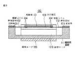
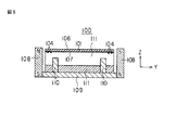
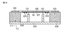
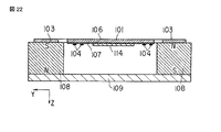
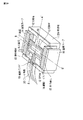
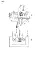
【解決手段】支持体103 と、光を反射するための鏡面が形成された可動板101 と、可動板101 と支持体103 との間を連結し、可動板101 を偏向可能に保持する弾性部材102 と、可動板101 が偏向運動する際の運動端近傍を通るよう可動板101上にリング状に形成された駆動コイル104 と、駆動コイル104 に対して可動板101 平面と略平行な方向に磁界を印加するための閉磁気回路を生成する磁石108 及び磁気ヨーク109,110 とを有する光偏向器において、閉磁気回路を生成する磁石108 又は磁気ヨーク109,110 を、駆動コイル104 の外側において可動板101 の運動端に対向する位置及び駆動コイル104 の内側において可動板101 に近接する位置に配置して磁気ギャップを形成する。
【選択図】 図2
Description
本発明はこのような課題に着目してなされたものであり、その第1の目的とするところは、可動部の剛性を向上させることによって高周波で駆動させたときでも不要な共振を発生せず、かつ駆動コイルにおける磁束密度を強めた閉磁気回路により可動部の駆動力を大きくして、少ない消費電力で大きな偏向角のとれる光偏向器及びその製造方法を提供することにある。
光を反射するための鏡面が形成された可動板と、
この可動板と前記支持体との間を連結し、前記可動板を偏向可能に保持する弾性部材と、
前記可動板が偏向運動する際の運動端近傍を通るよう前記可動板上にリング状に形成された駆動コイルと、
前記駆動コイルに対して前記可動板平面と略平行な方向に磁界を印加するための閉磁気回路を生成する磁石及び磁気ヨークとを有し、
前記閉磁気回路の磁気ギャップに位置する前記駆動コイルに交流電流を印加することで駆動力を発生させ、前記弾性部材の弾性変形により可動板の偏向運動を行う光偏向器において、
前記閉磁気回路を生成する前記磁石又は前記磁気ヨークを、前記駆動コイルの外側において前記可動板の運動端に対向する位置及び前記駆動コイルの内側において前記可動板に近接する位置に配置して前記磁気ギャップを形成したことを特徴とする光偏向器。
光を反射するための鏡面が形成された可動板と、
この可動板と前記支持体との間を連結し、前記可動板を偏向可能に保持する弾性部材と、
前記可動板が偏向運動する際の運動端近傍を通るよう前記可動板上にリング状に形成された駆動コイルと、
前記駆動コイルに対して前記可動板平面と略平行な方向に磁界を印加するための閉磁気回路を生成する磁石及び磁気ヨークとを有し、
前記閉磁気回路の磁気ギャップに位置する前記駆動コイルに交流電流を印加することで駆動力を発生させ、前記弾性部材の弾性変形により可動板の偏向運動を行う光偏向器において、
前記可動板上に前記閉磁気回路を生成する磁性部材をさらに設け、
前記閉磁気回路を生成する前記磁石又は前記磁気ヨークを、前記磁性部材に対向する位置に配置して前記磁気ギャップを形成したことを特徴とする光偏向器。
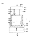
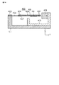
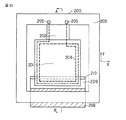
101…可動板、
102…弾性部材、
103…支持体、
104…駆動コイル、
105…電極パッド、
106…鏡面、
107…駆動コイル面、
108…永久磁石、
109、110…磁気ヨーク、
111…ベースフレーム。
Claims (8)
- 支持体と、
光を反射するための鏡面が形成された可動板と、
この可動板と前記支持体との間を連結し、前記可動板を偏向可能に保持する弾性部材と、
前記可動板が偏向運動する際の運動端近傍を通るよう前記可動板上にリング状に形成された駆動コイルと、
前記駆動コイルに対して前記可動板平面と略平行な方向に磁界を印加するための閉磁気回路を生成する磁石及び磁気ヨークとを有し、
前記閉磁気回路の磁気ギャップに位置する前記駆動コイルに交流電流を印加することで駆動力を発生させ、前記弾性部材の弾性変形により可動板の偏向運動を行う光偏向器において、
前記閉磁気回路を生成する前記磁石又は前記磁気ヨークを、前記駆動コイルの外側において前記可動板の運動端に対向する位置及び前記駆動コイルの内側において前記可動板に近接する位置に配置して前記磁気ギャップを形成したことを特徴とする光偏向器。 - 支持体と、
光を反射するための鏡面が形成された可動板と、
この可動板と前記支持体との間を連結し、前記可動板を偏向可能に保持する弾性部材と、
前記可動板が偏向運動する際の運動端近傍を通るよう前記可動板上にリング状に形成された駆動コイルと、
前記駆動コイルに対して前記可動板平面と略平行な方向に磁界を印加するための閉磁気回路を生成する磁石及び磁気ヨークとを有し、
前記閉磁気回路の磁気ギャップに位置する前記駆動コイルに交流電流を印加することで駆動力を発生させ、前記弾性部材の弾性変形により可動板の偏向運動を行う光偏向器において、
前記可動板上に前記閉磁気回路を生成する磁性部材をさらに設け、
前記閉磁気回路を生成する前記磁石又は前記磁気ヨークを、前記磁性部材に対向する位置に配置して前記磁気ギャップを形成したことを特徴とする光偏向器。 - 前記閉磁気回路を生成する前記磁石又は前記磁気ヨークを、前記駆動コイルの外側において前記可動板の運動端に対向する位置及び前記駆動コイルの内側において前記可動板に近接する位置に配置することを特徴とする請求項2記載の光偏向器。
- 前記閉磁気回路を生成する前記磁石又は前記磁気ヨークを、前記駆動コイルの外側において前記可動板の運動端に対向する位置に配置することを特徴とする請求項2記載の光偏向器。
- 前記支持体、前記弾性部材、前記可動板及び前記駆動コイルがモノリシックに一体形成されていることを特徴とする請求項1から4のいずれか1つに記載の光偏向器。
- 前記磁石は、前記可動板の駆動モーメントが最大となる位置に設けられていることを特徴とする請求項1から5のいずれか1つに記載の光偏向器。
- 固定用部材と、
互いに分離するように設けられ、前記固定用部材に固定するための支持体と、
光を反射するための鏡面を有する可動板と、
前記可動板と前記支持体との間を連結する弾性部材と、
前記弾性部材を弾性変形させて前記可動板を前記支持体に対して相対的に変位させる駆動手段と、を具備し、
少なくとも前記可動板と前記支持体と前記弾性部材とがモノリシックに一体成形されていることを特徴とする光偏向器。 - 固定用部材と、
互いに分離するように設けられ、前記固定用部材に固定するための支持体と、
光を反射するための鏡面を有する可動板と、
前記可動板と前記支持体との間を連結する弾性部材と、
前記弾性部材を弾性変形させて前記可動板を前記支持体に対して相対的に変位させる駆動手段と、
前記固定用部材に前記支持体を固定した後、除去可能なように前記支持体間を連結する連結部と、を具備する光偏向器を、
少なくとも前記可動板と前記支持体と前記弾性部材と前記連結部とをモノリシックに一体成形し、
前記ユニットを前記固定用部材に固定した後、前記連結部を除去し、
当該連結部を除去した前記固定用部材に対して前記駆動手段の一部を固定配置して製造することを特徴とする光偏向器の製造方法。
Priority Applications (1)
| Application Number | Priority Date | Filing Date | Title |
|---|---|---|---|
| JP2009223313A JP5143102B2 (ja) | 1997-12-09 | 2009-09-28 | 光偏向器の製造方法 |
Applications Claiming Priority (3)
| Application Number | Priority Date | Filing Date | Title |
|---|---|---|---|
| JP33882797 | 1997-12-09 | ||
| JP1997338827 | 1997-12-09 | ||
| JP2009223313A JP5143102B2 (ja) | 1997-12-09 | 2009-09-28 | 光偏向器の製造方法 |
Related Parent Applications (1)
| Application Number | Title | Priority Date | Filing Date |
|---|---|---|---|
| JP31348898A Division JP4414498B2 (ja) | 1997-12-09 | 1998-11-04 | 光偏向器 |
Publications (2)
| Publication Number | Publication Date |
|---|---|
| JP2010002926A true JP2010002926A (ja) | 2010-01-07 |
| JP5143102B2 JP5143102B2 (ja) | 2013-02-13 |
Family
ID=41584648
Family Applications (1)
| Application Number | Title | Priority Date | Filing Date |
|---|---|---|---|
| JP2009223313A Expired - Fee Related JP5143102B2 (ja) | 1997-12-09 | 2009-09-28 | 光偏向器の製造方法 |
Country Status (1)
| Country | Link |
|---|---|
| JP (1) | JP5143102B2 (ja) |
Cited By (7)
| Publication number | Priority date | Publication date | Assignee | Title |
|---|---|---|---|---|
| EP2216171A2 (en) | 2009-02-05 | 2010-08-11 | Nitto Denko Corporation | Reinforcing Material for Outer Panel and Method for Reinforcing Outer Panel |
| WO2013076844A1 (ja) * | 2011-11-24 | 2013-05-30 | パイオニア株式会社 | アクチュエータ |
| JP2014126626A (ja) * | 2012-12-26 | 2014-07-07 | Mitsubishi Electric Corp | レーザ加工装置 |
| CN103984091A (zh) * | 2013-11-21 | 2014-08-13 | 苏州浩创信息科技有限公司 | 一种扫描器摆镜装置 |
| JP2014200140A (ja) * | 2013-03-29 | 2014-10-23 | 日本信号株式会社 | プレーナ型アクチュエータ |
| US10114212B2 (en) | 2012-05-29 | 2018-10-30 | Kabushiki Kaisha Toyota Chuo Kenkyusho | Deflector |
| JP2023050829A (ja) * | 2021-09-30 | 2023-04-11 | 日本信号株式会社 | 磁気回路式ミラー駆動装置 |
Families Citing this family (1)
| Publication number | Priority date | Publication date | Assignee | Title |
|---|---|---|---|---|
| CN113514951B (zh) * | 2021-06-22 | 2024-01-30 | 歌尔光学科技有限公司 | 一种振镜系统、投影设备及投影方法 |
Citations (6)
| Publication number | Priority date | Publication date | Assignee | Title |
|---|---|---|---|---|
| JPS59191148A (ja) * | 1983-04-14 | 1984-10-30 | Mitsubishi Electric Corp | 偏向ミラ−装置 |
| JPS62210418A (ja) * | 1986-03-12 | 1987-09-16 | Hitachi Ltd | 光ビ−ム偏向ミラ− |
| JPH01195414A (ja) * | 1988-01-30 | 1989-08-07 | Konica Corp | ミラー振動子 |
| JPH03205623A (ja) * | 1989-10-31 | 1991-09-09 | Ricoh Co Ltd | 光情報記録再生装置のトラッキングミラーアクチュエーター装置 |
| JPH06175060A (ja) * | 1992-10-08 | 1994-06-24 | Fuji Electric Co Ltd | ねじり振動子および光偏向子 |
| JPH0719391B2 (ja) * | 1985-12-02 | 1995-03-06 | セイコーエプソン株式会社 | 光学式記録再生装置 |
-
2009
- 2009-09-28 JP JP2009223313A patent/JP5143102B2/ja not_active Expired - Fee Related
Patent Citations (6)
| Publication number | Priority date | Publication date | Assignee | Title |
|---|---|---|---|---|
| JPS59191148A (ja) * | 1983-04-14 | 1984-10-30 | Mitsubishi Electric Corp | 偏向ミラ−装置 |
| JPH0719391B2 (ja) * | 1985-12-02 | 1995-03-06 | セイコーエプソン株式会社 | 光学式記録再生装置 |
| JPS62210418A (ja) * | 1986-03-12 | 1987-09-16 | Hitachi Ltd | 光ビ−ム偏向ミラ− |
| JPH01195414A (ja) * | 1988-01-30 | 1989-08-07 | Konica Corp | ミラー振動子 |
| JPH03205623A (ja) * | 1989-10-31 | 1991-09-09 | Ricoh Co Ltd | 光情報記録再生装置のトラッキングミラーアクチュエーター装置 |
| JPH06175060A (ja) * | 1992-10-08 | 1994-06-24 | Fuji Electric Co Ltd | ねじり振動子および光偏向子 |
Cited By (8)
| Publication number | Priority date | Publication date | Assignee | Title |
|---|---|---|---|---|
| EP2216171A2 (en) | 2009-02-05 | 2010-08-11 | Nitto Denko Corporation | Reinforcing Material for Outer Panel and Method for Reinforcing Outer Panel |
| WO2013076844A1 (ja) * | 2011-11-24 | 2013-05-30 | パイオニア株式会社 | アクチュエータ |
| US10114212B2 (en) | 2012-05-29 | 2018-10-30 | Kabushiki Kaisha Toyota Chuo Kenkyusho | Deflector |
| JP2014126626A (ja) * | 2012-12-26 | 2014-07-07 | Mitsubishi Electric Corp | レーザ加工装置 |
| JP2014200140A (ja) * | 2013-03-29 | 2014-10-23 | 日本信号株式会社 | プレーナ型アクチュエータ |
| CN103984091A (zh) * | 2013-11-21 | 2014-08-13 | 苏州浩创信息科技有限公司 | 一种扫描器摆镜装置 |
| JP2023050829A (ja) * | 2021-09-30 | 2023-04-11 | 日本信号株式会社 | 磁気回路式ミラー駆動装置 |
| JP7760314B2 (ja) | 2021-09-30 | 2025-10-27 | 日本信号株式会社 | 磁気回路式ミラー駆動装置 |
Also Published As
| Publication number | Publication date |
|---|---|
| JP5143102B2 (ja) | 2013-02-13 |
Similar Documents
| Publication | Publication Date | Title |
|---|---|---|
| JP4414498B2 (ja) | 光偏向器 | |
| JP5143102B2 (ja) | 光偏向器の製造方法 | |
| US6188504B1 (en) | Optical scanner | |
| US6201629B1 (en) | Torsional micro-mechanical mirror system | |
| KR100236608B1 (ko) | 헤드액츄에이터 | |
| US6369400B2 (en) | Magnetic scanning or positioning system with at least two degrees of freedom | |
| US20080100898A1 (en) | Electromagnetic micro-actuator | |
| US20050018322A1 (en) | Magnetically actuated fast MEMS mirrors and microscanners | |
| US20020113675A1 (en) | Movable-body apparatus, optical deflector, and method of fabricating the same | |
| CN103282819B (zh) | 可磁驱动的微镜 | |
| JP2002361174A (ja) | 振動アクチュエータ装置 | |
| JP2004126503A (ja) | マイクロアクチュエータ及びこれを用いた光スイッチ | |
| JPH08334723A (ja) | 光偏向素子 | |
| JP4197776B2 (ja) | 光スキャナ | |
| US6813049B2 (en) | Torsional rocking structural component | |
| JP3684003B2 (ja) | 光スキャナ | |
| JP4036643B2 (ja) | 光偏向器及び光偏向器アレイ | |
| JPH10123449A5 (ja) | ||
| JP6180074B2 (ja) | プレーナ型電磁アクチュエータ | |
| JP2002350457A (ja) | 揺動体 | |
| US20240387086A1 (en) | Driving element and driving device | |
| JP3776521B2 (ja) | 光スキャナ | |
| JP2002090684A (ja) | 光走査装置及びその製造方法 | |
| JPH1090625A5 (ja) | ||
| JP4882595B2 (ja) | 光スキャナおよび画像形成装置 |
Legal Events
| Date | Code | Title | Description |
|---|---|---|---|
| A521 | Written amendment |
Free format text: JAPANESE INTERMEDIATE CODE: A523 Effective date: 20091028 |
|
| A621 | Written request for application examination |
Free format text: JAPANESE INTERMEDIATE CODE: A621 Effective date: 20091028 |
|
| A131 | Notification of reasons for refusal |
Free format text: JAPANESE INTERMEDIATE CODE: A131 Effective date: 20121002 |
|
| A521 | Written amendment |
Free format text: JAPANESE INTERMEDIATE CODE: A523 Effective date: 20121029 |
|
| TRDD | Decision of grant or rejection written | ||
| A01 | Written decision to grant a patent or to grant a registration (utility model) |
Free format text: JAPANESE INTERMEDIATE CODE: A01 Effective date: 20121113 |
|
| A01 | Written decision to grant a patent or to grant a registration (utility model) |
Free format text: JAPANESE INTERMEDIATE CODE: A01 |
|
| A61 | First payment of annual fees (during grant procedure) |
Free format text: JAPANESE INTERMEDIATE CODE: A61 Effective date: 20121120 |
|
| FPAY | Renewal fee payment (event date is renewal date of database) |
Free format text: PAYMENT UNTIL: 20151130 Year of fee payment: 3 |
|
| S531 | Written request for registration of change of domicile |
Free format text: JAPANESE INTERMEDIATE CODE: R313531 |
|
| R350 | Written notification of registration of transfer |
Free format text: JAPANESE INTERMEDIATE CODE: R350 |
|
| LAPS | Cancellation because of no payment of annual fees |