JP2009544040A - High speed signal testing system with oscilloscope functionality - Google Patents
High speed signal testing system with oscilloscope functionality Download PDFInfo
- Publication number
- JP2009544040A JP2009544040A JP2009520920A JP2009520920A JP2009544040A JP 2009544040 A JP2009544040 A JP 2009544040A JP 2009520920 A JP2009520920 A JP 2009520920A JP 2009520920 A JP2009520920 A JP 2009520920A JP 2009544040 A JP2009544040 A JP 2009544040A
- Authority
- JP
- Japan
- Prior art keywords
- signal
- time reference
- high speed
- bit
- clock signal
- Prior art date
- Legal status (The legal status is an assumption and is not a legal conclusion. Google has not performed a legal analysis and makes no representation as to the accuracy of the status listed.)
- Pending
Links
Images


Classifications
-
- G—PHYSICS
- G01—MEASURING; TESTING
- G01R—MEASURING ELECTRIC VARIABLES; MEASURING MAGNETIC VARIABLES
- G01R31/00—Arrangements for testing electric properties; Arrangements for locating electric faults; Arrangements for electrical testing characterised by what is being tested not provided for elsewhere
- G01R31/28—Testing of electronic circuits, e.g. by signal tracer
- G01R31/317—Testing of digital circuits
- G01R31/3181—Functional testing
- G01R31/319—Tester hardware, i.e. output processing circuits
- G01R31/3193—Tester hardware, i.e. output processing circuits with comparison between actual response and known fault free response
- G01R31/31932—Comparators
-
- G—PHYSICS
- G01—MEASURING; TESTING
- G01R—MEASURING ELECTRIC VARIABLES; MEASURING MAGNETIC VARIABLES
- G01R31/00—Arrangements for testing electric properties; Arrangements for locating electric faults; Arrangements for electrical testing characterised by what is being tested not provided for elsewhere
- G01R31/28—Testing of electronic circuits, e.g. by signal tracer
- G01R31/317—Testing of digital circuits
- G01R31/3181—Functional testing
- G01R31/319—Tester hardware, i.e. output processing circuits
- G01R31/3193—Tester hardware, i.e. output processing circuits with comparison between actual response and known fault free response
-
- G—PHYSICS
- G01—MEASURING; TESTING
- G01R—MEASURING ELECTRIC VARIABLES; MEASURING MAGNETIC VARIABLES
- G01R13/00—Arrangements for displaying electric variables or waveforms
- G01R13/02—Arrangements for displaying electric variables or waveforms for displaying measured electric variables in digital form
Landscapes
- Engineering & Computer Science (AREA)
- General Engineering & Computer Science (AREA)
- Physics & Mathematics (AREA)
- General Physics & Mathematics (AREA)
- Tests Of Electronic Circuits (AREA)
Abstract
ハイスピード信号テスティング・システムであって、オシロスコープの機能性を有するパターン・テスタを、極小の実現コストで提供するためのデジタル回路を備えたものである。このデジタル回路は、ハイスピード繰り返し時間基準信号を供給する時間基準発生器を備えている。この時間基準信号は、サブサンプラ及び蓄積メモリと共に、本システムが1以上の関心のビットを拡大し、その部分を分析することを可能なようにするものであり、該1以上の関心のビットは、被テスト信号上に存在する繰り返しパターン内のものである。そのような関心の部分は、立ち上がり及び立ち下がりのエッジ、並びに一定の高いビット値及び低いビット値を含んでいる。
【選択図】図2A high-speed signal testing system comprising a digital circuit for providing a pattern tester having oscilloscope functionality at a minimal realization cost. The digital circuit includes a time reference generator that provides a high speed repeat time reference signal. This time reference signal, together with the subsampler and storage memory, allows the system to expand one or more bits of interest and analyze that portion of the one or more bits of interest, It is in a repetitive pattern existing on the signal under test. Such portions of interest include rising and falling edges, as well as certain high and low bit values.
[Selection] Figure 2
Description
この出願は、米国仮特許出願第60/830,797号の優先権の利益を主張しており、この米国仮特許出願第60/830,797号は、2006年7月14日に提出され、「主にデジタルな時間基準発生器を使用する信号完全性測定のシステム及び方法」という発明の名称であり、ここに、その全体を参照によって組み込むものとする。 This application claims the benefit of priority of US Provisional Patent Application No. 60 / 830,797, which was filed on July 14, 2006, It is the title of the invention, "Signal integrity measurement system and method using primarily digital time reference generator", which is hereby incorporated by reference in its entirety.
本発明は、一般的に、ハイスピード・デジタル・データの測定に関する。より詳細には、本発明は、オシロスコープの機能性を有するハイスピード信号テスティング・システムに向けられている。 The present invention generally relates to the measurement of high speed digital data. More particularly, the present invention is directed to a high speed signal testing system having oscilloscope functionality.
半導体部品内部、半導体部品間、及びボードとキャビネット間のデジタル通信のスピードは、増大を続けている。スピードが増大するにつれ、デジタル信号をテストすることは、ロジック(パターン)のテスティングを必要とするだけでなく、アナログ・パラメータのテスティングも要求している。スピードが増大すると、バイナリのデジタル・データを表す電圧波形のアナログ形状は、重要である。貧弱なアナログ・パラメータ、例えば、余りにも長い立ち上がり時間又は余りにも小さな電圧の幅は、長期的な課題を招いている可能性があり、これらは、クイック・パターン・テストを使用して明らかにできない。逆に、また、アナログ・パラメータのテスティングは、ロジック又はパターンのテストにおいて、不具合をデバックするときに有用である。そのような不具合は、波形の形状又はタイミングのジッタに自ずと現れるシステマチックな現象によって引き起こされている可能性がある。 The speed of digital communication within semiconductor components, between semiconductor components, and between boards and cabinets continues to increase. As speed increases, testing digital signals not only requires logic (pattern) testing, but also requires analog parameter testing. As speed increases, the analog shape of the voltage waveform representing binary digital data becomes important. Poor analog parameters, such as too long rise times or too small voltage ranges, can lead to long-term challenges, which cannot be revealed using quick pattern testing . Conversely, analog parameter testing is useful when debugging failures in logic or pattern testing. Such a failure may be caused by a systematic phenomenon that naturally appears in the waveform shape or timing jitter.
当業の現状では、ロジックのテスティング及びアナログ・パラメータのテスティングをそれぞれ実行するために、しばしば、別々の機器が必要となる。例えば、パターンのテスティングに対してロジック・アナライザ又はビットエラーレート・テスタ(BERT)を使用し、アイ・ダイアグラムのテスティング又はジッタのテスティングに対してオシロスコープ又はジッタ・アナライザを使用している。ピン数の多いデバイス又は回路へのハイスピード・デジタル信号をテストする必要性がより急増するにつれて、様々な機器の能力の幾つかを組み合わせる必要性が生じている。また、デバイス又は小さなフォーム・ファクタにおいて、そのような能力を集積する必要性が存在し、該デバイス又は小さなフォーム・ファクタは、アプリケーション・デバイス又はアプリケーション・ボードに取り付け可能なものである。例えば、テスト関係のモジュール又は部品をシステム上に配置し、上記のデジタルのテスティングの機能を実行させることが可能である。多くのハイスピード・シリアル受信機は、今や、デジタルのテスティングの目的で、パターン・チェッカを備えている。この基本的なパターン・チェッキング能力にオシロスコープの能力を追加することは、大いに望まれていることであるが、自明なことではない。 In the current state of the art, separate equipment is often required to perform logic testing and analog parameter testing, respectively. For example, a logic analyzer or bit error rate tester (BERT) is used for pattern testing, and an oscilloscope or jitter analyzer is used for eye diagram testing or jitter testing. As the need to test high speed digital signals to high pin count devices or circuits has increased more so, there has been a need to combine some of the capabilities of various equipment. There is also a need to integrate such capabilities in a device or small form factor, which can be attached to an application device or an application board. For example, it is possible to place a test-related module or component on the system and execute the above-described digital testing function. Many high-speed serial receivers now have a pattern checker for digital testing purposes. Adding oscilloscope capabilities to this basic pattern checking capability is highly desirable but not trivial.
商業上のテスト機器を使用する一例として、BERT又はロジック・アナライザがアイ・ダイアグラム分析を実行できるようにすることは、テスティングを単純化し、2つに代わって1つの機器を用いて強化された範囲を提供することになる。そのような機器は、既に存在している。しかし、パターンのテスティングとアナログ・パラメータのテスティングとの間に背反する要求が与えられると、そのような二重機能の機器を生成することは、該機器の基本的なアーキテクチャに対する込み入った修正を引き起こし、拡張性を制限することになる。特に、BERTがアイ・ダイアグラムを発生できるようにするために、前者は2つの主要なやり方で修正されることになる。第1に、アナログ遅延線回路を導入することになり、このアナログ遅延線回路は、データ信号若しくはクロック信号、又はそれらの両方を、非常に小さな量(データ・パターンの単位間隔の何分の一か)だけ遅延可能である。該遅延線回路は、面積を消費し、帯域幅を制限し、較正が困難である。現代のアプリケーション、又はパターン・テスタがシステム内部に集積されるアプリケーションの場合、複数のテスト・チャンネルが必要となるときに扱いにくくなってしまう。 As an example of using commercial test equipment, allowing a BERT or logic analyzer to perform eye diagram analysis has simplified testing and has been enhanced with one equipment instead of two. Will provide a range. Such equipment already exists. However, given the conflicting requirements between pattern testing and analog parameter testing, creating such a dual-function device is a complicated modification to the basic architecture of the device. Will limit the extensibility. In particular, the former will be modified in two main ways to allow the BERT to generate an eye diagram. First, an analog delay line circuit will be introduced, and this analog delay line circuit will transfer a data signal or clock signal, or both, in a very small amount (a fraction of the unit interval of the data pattern). Can only be delayed. The delay line circuit consumes area, limits bandwidth, and is difficult to calibrate. For modern applications, or applications where pattern testers are integrated within the system, it becomes cumbersome when multiple test channels are required.
必要となる他の修正は、フロントエンドのキャプチャ・エレクトロニクスを伴うことになる。特に、ロジックのテスティングは、当該機器のフロント・エンドに電圧コンパレータを単に必要とするだけであるが、一方、アイ・ダイアグラム等の測定は、より複雑な回路を必要とする。BERTがアイ・ダイアグラムの測定を実行するよう修正するために、技術者たちは、ウィンドウ・コンパレータ(類似のものであるが、わずかにオフセットのある閾値レベルを有する2つ以上の電圧コンパレータ)を生成し、非常に狭い電圧平面及び関連した時間ポイントを介して遷移を検出している。あるいは、2つ以上のコンパレータを配置してウインドウ比較を実行することに替えて、別の実現は、単一の電圧コンパレータに加える2つのわずかに遅延させたストローブを必要としており、この遅延は、上記データ・パターンの単位間隔のごくわずかな割合である。このアプローチは、やはり面倒なものであり、非常にハイスピードなときの実現が困難である。 Other modifications that would be required would involve front-end capture electronics. In particular, logic testing simply requires a voltage comparator at the front end of the device, while measurements such as eye diagrams require more complex circuitry. To modify the BERT to perform eye diagram measurements, engineers generate window comparators (similar but two or more voltage comparators with slightly offset threshold levels) However, it detects transitions through very narrow voltage planes and associated time points. Alternatively, instead of placing two or more comparators to perform the window comparison, another implementation requires two slightly delayed strobes added to a single voltage comparator, which delay is This is a very small percentage of the unit interval of the data pattern. This approach is still cumbersome and difficult to achieve at very high speeds.
本発明の一態様は、ハイスピード繰り返しデータ信号をテストするためのシステムであって、基準クロック信号に応答し、それによってハイスピード繰り返し信号を発生させるための時間基準発生器と、前記ハイスピード繰り返し信号の関数として、前記ハイスピード繰り返しデータ信号をデジタル化された信号にデジタル化するための1ビット電圧デジタイザと、前記デジタル化された信号と選択したデジタル値とを比較し、前記ハイスピード繰り返し信号の関数としてコンパレータの結果を出力するためのデジタル・コンパレータと、前記ハイスピード繰り返し信号に応答し、それによって遅くなったクロック信号を生み出すビットシフト及び周波数分周器のブロックと、前記遅くなったクロック信号の関数として前記コンパレータの結果をサブサンプリングし、それによってサブサンプリングされた結果を出力するためのサブサンプラと、前記ハイスピード繰り返し信号の関数として書き込みアドレスを供給するための、Nを法とするアドレス・カウンタと、前記遅くなったクロック信号の関数として前記サブサンプリングされた結果のうちの1つ1つを記憶し、前記書き込みアドレスの1つ1つのそれぞれと対応させるための蓄積メモリとを備えた、システムである。 One aspect of the present invention is a system for testing a high speed repetitive data signal, wherein the time reference generator is responsive to a reference clock signal, thereby generating a high speed repetitive signal, and the high speed repetitive signal. A 1-bit voltage digitizer for digitizing the high-speed repetitive data signal into a digitized signal as a function of the signal, comparing the digitized signal with a selected digital value, and the high-speed repetitive signal A digital comparator for outputting the result of the comparator as a function of: a block of bit shift and frequency dividers responsive to the high speed repetitive signal, thereby producing a delayed clock signal, and the delayed clock The result of the comparator as a function of signal A subsampler for subsampling and thereby outputting a subsampled result, an address counter modulo N for providing a write address as a function of the high speed repetitive signal, and the slow And a storage memory for storing each of the subsampled results as a function of a clock signal and corresponding to each of the write addresses.
本発明の別態様は、オシロスコープ回路を備えたハイスピード繰り返しデータ信号をテストするためのシステムであって、基準クロック信号に応答し、それによってハイスピード繰り返し信号を発生させる時間基準発生器と、前記ハイスピード繰り返し信号の関数として、前記ハイスピード繰り返しデータ信号をデジタルされた信号にデジタル化するための1ビット電圧デジタイザと、長さBを有する基準ビット・パターンを記憶するための基準パターン・メモリと、前記基準ビット・パターンと一定のビット値との間で選択し、それによって選択されたデジタル値を出力するためのセレクタと、前記デジタル化された信号と前記選択されたデジタル値とを比較し、前記ハイスピード繰り返し信号の関数としてコンパレータの結果を出力するためのデジタル・コンパレータと、前記ハイスピード繰り返し信号に応答し、それによって遅くなったクロック信号を生み出すビットシフト及び周波数分周器のブロックであって、Bによって前記ハイスピード繰り返し信号を分周する前記ビットシフト及び周波数分周器のブロックと、前記遅くなったクロック信号の関数として前記コンパレータの結果をサブサンプリングし、それによってサブサンプリングされた結果を出力するためのサブサンプラと、前記ハイスピード繰り返し信号の関数として書き込みアドレスを供給するための、Nを法とするアドレス・カウンタと、前記遅くなったクロック信号の関数として前記サブサンプリングされた結果のうちの1つ1つを記憶し、前記書き込みアドレスのうちの1つ1つのそれぞれと対応させるための蓄積メモリとを前記オシロスコープ回路が備えた、システムである。 Another aspect of the present invention is a system for testing a high speed repetitive data signal with an oscilloscope circuit, wherein the time reference generator is responsive to a reference clock signal and thereby generates a high speed repetitive signal; A 1-bit voltage digitizer for digitizing the high-speed repetitive data signal into a digitized signal as a function of the high-speed repetitive signal; and a reference pattern memory for storing a reference bit pattern having a length B A selector for selecting between the reference bit pattern and a constant bit value and thereby outputting a selected digital value, and comparing the digitized signal with the selected digital value Output the result of the comparator as a function of the high-speed repetition signal A digital comparator and a bit shift and frequency divider block that is responsive to the high speed repeat signal and thereby produces a delayed clock signal, wherein the high speed repeat signal is divided by B A block of bit shift and frequency dividers, a subsampler for subsampling the result of the comparator as a function of the slowed clock signal and thereby outputting the subsampled result, and a high-speed repetitive signal An address counter modulo N for supplying a write address as a function, and storing each one of the subsampled results as a function of the delayed clock signal; Correspond to each one of them The oscilloscope circuit and the storage memory for the provided a system.
本発明のまた別の態様は、オシロスコープを実現してハイスピード・データ信号を分析するための方法であって、時間基準スパンNを有する繰り返し時間基準信号に応答して、前記ハイスピード・データ信号を1ビットのデジタル化された信号にデジタル化するステップと、前記繰り返し時間基準信号に応答して前記1ビットのデジタル化された信号と一定のビット値とを比較するステップであって、それによってコンパレータの出力を発生させる、ステップと、前記繰り返し時間基準信号を分周するステップであって、それによってハイスピード・データの周期に対応する遅くなったクロック信号を生成する、ステップと、前記遅くなったクロック信号に応答して前記コンパレータの結果をサブサンプリングするステップであって、それによってサブサンプリングされた結果を出力する、ステップと、前記繰り返し時間基準信号の関数として、Nを法とする書き込みアドレスを発生させるステップと、前記遅くなったクロック信号に応答して前記サブサンプリングされた結果のうちの1つ1つをメモリに記憶し、前記書き込みアドレスのうちの1つ1つのそれぞれを対応させるステップとを含む、方法である。 Another aspect of the present invention is a method for implementing an oscilloscope to analyze a high speed data signal, wherein the high speed data signal is responsive to a repetitive time reference signal having a time reference span N. Digitizing a 1-bit digitized signal and comparing the 1-bit digitized signal with a constant bit value in response to the repetition time reference signal, thereby Generating a comparator output; and dividing the repetitive time reference signal, thereby generating a delayed clock signal corresponding to a period of high-speed data; and Sub-sampling the comparator result in response to the clock signal, comprising: Outputting a subsampled result, generating a write address modulo N as a function of the repetition time reference signal, and subsampling in response to the delayed clock signal Storing each one of the results in a memory and associating each one of the write addresses with each other.
本発明を図解する目的のため、当該図面は本発明の1以上の実施形態の態様を示している。しかし、本発明は、これら図面に示した正確な配列及び手段に限定されないことは理解されたい。 For the purpose of illustrating the invention, the drawings illustrate aspects of one or more embodiments of the invention. However, it should be understood that the invention is not limited to the precise arrangements and instrumentality shown in these drawings.
図1は、先行技術のデジタル・パターン・テスタ10を示しており、それは、該テスタに入力される入力信号14の論理的完全性をテストするためのものである。上記の背景技術の節で述べたように、テスタ10は、ハイスピード・デジタル通信デバイス(図示せず)の設計の一部である可能性があるか、又は、BERT若しくはロジック・アナライザ等の独立型の機器である可能性がある。テスタ10のフロントエンドは、入ってくる信号14の電圧を「スライス」し、それから論理値を復元する電圧コンパレータ18である。この論理値は、上記の入力信号がコンパレータ18の電圧閾値より大きいときに「1」を、そうでないときに「0」である。次に、デジタル・コンパレータ22を使用して、オンボードのメモリ30に記憶された基準パターン26に対し、ビット対ビットでこの論理値を比較する。エラー・カウンタ34は、一方では入力信号14に由来するこの論理値と、他方では基準パターン26の対応するそれぞれのビットとの間の不一致の数を追跡し続ける。
FIG. 1 shows a prior art
デジタル・コンパレータ22は、オンボード・クロック信号38によってクロックされ、オンボード・クロック信号38は、比較される上記のデータ・ビットの中央に集中するものである。このことは、サンプリング・エラーの可能性を最小化する。このアーキテクチャによると、上記のセンタリング動作は、上記のクロック信号に対する遅延線(図示せず)、又はクロックアンドデータ回復(CDR)回路等の位相追跡回路(図示せず)の何れかで起きることになる。後者のシナリオは、インシステム・アプリケーションにおいて、より日常的なものである。また、デジタル・パターン整列ブロック(図示せず)が場合によって備わっており、このデジタル・パターン整列ブロックは、基準パターン26を、最少量のエラーが観測されるまでシフトするものである。何れの場合においても、テスタ10に供給される基準クロック42は低い周波数であることが可能であり、この低い周波数は、典型的には位相ロック・ループ(PLL)逓倍器46を使用して、後の逓倍で目標のハイスピード周波数にするものである。一例において、逓倍は、100MHzのクロック信号を5GHzのサンプリング信号まで増大させることが可能である。
The
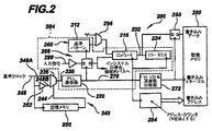
今、図2を参照すると、この図は、例示のデジタル・パターン・テスティング・システム200を示しており、それは、遷移又は非遷移のビットのオシロスコープの軌跡をキャプチャ可能にするオシロスコープの特徴を備えている。図1と2とを互いに比較すると視覚的に容易にわかるように、例示のテスティング・システム200は、図1のパターン・テスタの設計に基づいており、その主要な部品を、破線アウトライン204の内部に設置している。即ち、図1のテスタ10のように、図2のテスティング・システム200は、フロント・エンド電圧コンパレータ208と、基準パターン・メモリ212と、デジタル・コンパレータ216と、周波数スケーリングPLL逓倍器220と、エラー・カウンタ224とを備えている。図1と2とを互いに比較すると更にわかるように、図2の破線アウトライン204の内部の従来のテスタの部品に対してなされた追加は、PLL逓倍器220の入力228と、デジタル・コンパレータ216の出力232とに対する追加を含んでいる。わかるように、これらの修正の両方は性質においてデジタルであり、従来の方法を使用することの前述のリスクを大して伴わずに実現可能である。
Referring now to FIG. 2, this figure shows an exemplary digital
第1の修正において、高い周波数の時間基準発生器240を提供するために、PLL逓倍器220の入力228は、マルチプレクサ236及び後述する他の部品の後にあり、高い周波数の時間基準発生器240は、例えば、2007年7月12日に提出され、「主にデジタルな時間基準発生器を使用する信号完全性測定のシステム及び方法」という発明の名称である米国特許出願第11/776,825号に記載されている時間基準発生器のうちの任意の1つであることができ、時間基準発生器に関し開示している全て対し、ここに、参照によって組み込むものとする。示した例において、マルチプレクサ236は、2つの入力間で絶えず選択する選択信号244に応答しており、この場合において、これら2つの入力は、入ってくる基準クロック信号248の2つのバージョン、遅延していないバージョン248Aと、粗い遅延252を使用して遅延させた粗く遅延したバージョン248Bとである。粗い遅延は、従来技術を使用して確実に構築可能な最小遅延よりも実質的に大きな任意の遅延として定義している。典型的に、そのような遅延は、ハイ・スピード通信デバイスにおける最小ビット周期と等価である。しかし、一般的に、そして上記の’825出願に記載されているように、マルチプレクサ236への上記の選択可能入力信号は、互いに関して粗く遅延させた任意の2つ以上のクロック信号であることができる。この例において、選択信号244は、オンボードの循環メモリ256からやって来るものであり、オンボードの循環メモリ256は、やって来る基準クロック248によってクロックしている。PLL逓倍器220と、マルチプレクサ236と、クロック信号248の遅延したバージョン248Bを作成するための粗い遅延252と、選択信号244と、この選択信号を駆動するオンボードのメモリ256との組合せは、時間基準発生器240を構成しており、時間基準発生器240は、従来のシステムにおいて必要とされた何らかのアナログ遅延線を置き換えるものである。アナログ・ロジックを越える、デジタル・ロジックを使用することの、とりわけインシステム・アプリケーションにおける利点は、当業者に良く知られている。
In a first modification, to provide a high frequency
ウィンドウ・コンパレータ又はより面倒なフロントエンドを実現することなくオシロスコープの測定を可能にするために、時間基準発生器240に加えて、電圧コンパレータ208のデジタル・ロジックのダウン・ストリームは、例えば、図2に示しているように修正している。第1に、オシロスコープ・モードの間、基準パターン260は、一定の論理的な値、例えば0で置き換わることが可能である。このオシロスコープ・モードと上記のビットパターンのテスティング・モードとの間の選択は、例えば、上記の一定の論理的0信号と基準パターン・メモリ212の出力との間の選択を可能にするマルチプレクサ264によって容易にすることが可能である。デジタル・コンパレータ216は、簡単にするために、所望ならば図1のデジタル・コンパレータ22と同じままであることが可能である。加えて、上記オシロスコープ・モードにおいて、エラー・カウンタ224は、サブサンプリング・フリップフロップ268によってバイパスし置き換えることができる。簡潔に述べると、サブサンプリング・フリップフロップ268は、テストされるハイスピード・パターンにおける単一のビットの上へのロッキングの機能を果たすものである。
In addition to the
事実上、本システムは、テスティング・システム200がオシロスコープ・モードにあるときに、上記のパターンの特定のエッジ又は他の部分を拡大してそれを分析するように設計している。このことを達成するために、サブサンプリング・フリップフロップ268は、ビットシフト及び周波数分周器のブロック272により駆動しており、ビットシフト及び周波数分周器のブロック272は、時間基準発生器240の出力276に応答するものである。ビットシフト及び周波数分周器のブロック272の周波数分周は、パターン260の長さBに等しい値に設定する。パターン260が127ビットのパターン長Bを有する擬似ランダム・ビット・シーケンス(PRBS)である場合、この周波数分周器の値は127である。ビットシフト及び周波数分周器のブロック272のビット・シフティング動作は、この遅くなったクロックを単一ビットの増分で移動させ、それをオリジナルの周期的なテスト・パターン260内の127の位置それぞれに配置することが可能である。図3は、11の長さBを有するパターン260Aに対する、ビットシフト及び周波数分周器のブロック272(図2)の動作を示している。ビットシフト及び周波数分周器のブロック272の、シフトさせた11の出力である出力1から出力B(B=11)を図解している。これらの出力のうちの任意の1つは、所与の時刻に発生する。この図から直感的なように、サブサンプリング・フリップ・フロップ268(図2)が見るのは、1データ・ビートごとではなく、11データ・ビートごとのデジタル比較の結果である。それは、繰り返すパターン260A全体の中の、単一のビットに対する上記の比較の結果を見るのみである。
In effect, the system is designed to magnify and analyze specific edges or other parts of the pattern when the
再び図2を参照すると、上記のサブサンプリングされる比較動作の出力は、蓄積メモリ280に蓄積することができ、蓄積メモリ280は、時間基準発生器240によってクロックするアドレス・カウンタ284を備えている。このやり方でのアドレス・カウンタ284を使用するアドレッシングの重要性は、後述する。今のところは、ビットシフト及び周波数分周器のブロック272の分周比が図2におけるパターン長Bに等しく、蓄積結果はばらばらの順序で蓄積メモリに到着する可能性があるものの、あるガイドラインに従う場合、上記のメモリにおける全ての場所がカバーされる(以下を見よ)からであることに注意されたい。
Referring again to FIG. 2, the output of the subsampled comparison operation can be stored in
上記の’825特許出願において詳細に述べるように、PLL逓倍器220がその出力276を切り替える各々の時刻は、わずかに遅延する。従って、電圧コンパレータ208がクロックされるたびに、それは入力信号288のやって来るビット・ストリームを、わずかに異なる遅延でストローブする。同じように、ビットシフト及び周波数分周器のブロック272の上記の遅くなったクロックでサブサンプリング・フリップ・フロップ268をクロックするときはいつも、それもまた、わずかに異なる遅延に対応することになる。時間基準発生器240をプログラムし、一定のランプを発生させた(時間基準発生器のプログラミングの記載に対しては、上記の’825特許出願を見よ)場合、PLL逓倍器220の出力276は、上記のランプの振る舞いに従い、固定量だけ、常に進むか又は遅れることになる。蓄積メモリ280における各入力は、PLL逓倍器220からの単一の遅延値に対応するように設計している。従って、及び図4を参照すると、上記の時間基準ランプの1つの完全な掃引の終わりで、蓄積メモリ280は時間領域の波形400を含むことになり、時間領域の波形400は、拡大している遷移ビットが電圧コンパレータ208(図2)の電圧閾値より高いかそうでないかに対応するものである。
Each time that
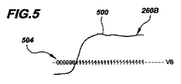
電圧コンパレータ208の上記閾値電圧がプログラム可能である場合、この閾値電圧を掃引することは、ウィンドウ・コンパレータ又は追加のストローブ回路を必要とすることなく、関心のデータ・ビットに対する完全な電圧波形を発生させることを補助する可能性がある。図2及び5を参照すると、図5は、電圧コンパレータ208(図2)の上記閾値を固定値VBに設定し、そしてデータ・パターン260Bの関心のビット500に対して、時間基準発生器を動作させることを図解している。その結果は、1と0とのシーケンス504であり、それは、蓄積メモリ280に記憶することができる。電圧コンパレータ208の上記閾値電圧を増分し、時間基準発生器240を再び動作させると、1と0との別のシーケンスが発生し、それは先のセットに追加される。掃引が進むにつれ、図6に示す温度計符号600のような温度計符号が得られる。もちろん、この例示の実現において、該温度計符号の値は、蓄積メモリ280に直接蓄積している。なお、この動作は、ビット・エラー・レート(BER)の等高線図の動作とは異なる。この動作は、文字通り、反復性の電圧遷移のデジタル化動作である。それは、BERがするようなやり方で、エラー・カウントを表していない。
If the threshold voltage of the
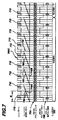
図2の蓄積メモリ280及び時間基準発生器240に戻ると、被テストの繰り返すパターン260に関する蓄積メモリ280の長さ(及び時間基準のランプの長さ)の特定の選択が必要である。最も単純化すると、測定されるデータ・パターン260が偶数の長さを持つ場合、蓄積メモリ280(デジタル化処理における時間軸を表している)の長さは、奇数の数の場所を持つように選択している。逆に、上記のパターン長が奇数である場合、蓄積メモリ280(及び対応する時間基準発生器のランプ)の長さは、偶数である。図2及び7を参照すると、図7は、例示のテスト・パターン260C(図2)と、時間基準発生器240によって出力される例示の時間遅延値700と、例示のメモリ・アドレス値704と、及び上記のメモリ値が埋まる順番708とを示している。この図において、パターン260Cは、5ビットの長さB及び関心のビット712を有している。時間基準発生器240は、8のビット値に等価な時間期間において、その様々な遅延を介して傾斜する。わかるように、上記のPLLランプ及び上記のビット・ストリームの繰り返しの十分な数が並べられている限り、メモリ値704の全てが最終的に埋まることになる。蓄積メモリ280の長さを適正に選択しない場合、エイリアシングの効果が生じ、間違った測定がなされてしまう。一般的に、上記の時間基準ランプの繰り返しの数又はビット・パターン260Cの繰り返しの数は、パターン長Bと時間基準スパンNとの間の最小公倍数に対応する。図7の例において、5と8との間の最小公倍数は40である。従って、パターン260Cの8(又は上記の時間基準ランプの5)の繰り返しが必要となる。また図7を参照して、示しているタイミング波形716の始まり716Aにおいて、PLL逓倍器220がその出力遅延を切り替え傾斜し続けるにつれて、それがどのように関心のビット712(関心の遷移)に2回出くわすのかに注目せよ。このことは、電圧コンパレータ208が、最初は小さな遅延で、それから続いて大きな遅延で、特定のビット712(遷移)をサンプリングすることを意味している。ランプ・タイミング波形716の次の繰り返し716Bにおいて、PLL逓倍器220は再び繰り返し同じ遷移に出くわすが、その各々のときに、それは遅延値700のうちの一意の1つを伴ってそれに出くわすことになる。
Returning to the
蓄積メモリ280の長さに関係して、上記の時間基準スパンは、典型的に、数百(例えば、512)程度のサンプルであり、なぜなら、さらに大きなタイミング解像度を生成することはやりすぎになるからである。ビット・パターン260の長さBは、一方で、さらに小さいか(例えば、上記の例における5)、又はさらに大きい(例えば、数千のビット)であることが可能である。
With respect to the length of the
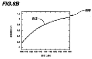
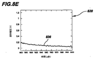
図8Aは、デジタル・ビット・ストリームの例804の出力プロット800の例を示しており、これは、オシロスコープを使用可能な本開示に従い製作したテスティング・システム、例えば図2のデジタル・パターン・テスティング・システム200の、オシロスコープの機能性を使用して発生させたものである。帯域幅の制限及び損失の多い伝送のために、ビット・ストリーム804は、ゆっくりとした立ち上がり時間及び深刻な電圧ノイズを示している。これらの影響は、オシロスコープを使用可能な本開示のテスティング・システムを使用してテストされるものの例である。図8Bは、オシロスコープを強化した本開示のテスティング・システム、例えば図2のデジタル・パターン・テスティング・システム200によって発生させたプロットの例808を示しており、立ち上がり遷移812をこのテスティング・システムが拡大したときのものである。図8Cは、オシロスコープを強化した本開示のテスティング・システム、例えば図2のデジタル・パターン・テスティング・システム200によって発生させたプロットの例816を示しており、立ち下がり遷移820をこのテスティング・システムが拡大したときのものである。図8D及び8Eは、それぞれ、オシロスコープを強化した本開示のテスティング・システム、例えば図2のデジタル・パターン・テスティング・システム200によって発生させた例示のプロット824及び828であり、一定の高いビット値832及び一定の低いビット値836それぞれをこのテスティング・システムが拡大したときのものである。
FIG. 8A shows an example of an
わかるように、オシロスコープを使用可能な本開示のテスティング・システムは、デジタル・ビット・ストリーム内の問題領域を確認することにおいて、大きな実用性を有している。例えば、今や、あるビット・ストリームにおける各遷移の平均到着時刻が利用可能になったので、データ依存ジッタを容易に抽出することが可能である。図9は、2つの立ち上がり遷移904及び908の重ねあわせを含んだ例示のプロット900を示しており、これら2つの立ち上がり遷移904及び908は、データ依存のジッタを呈している。容易にわかるように、遷移904及び908は、異なる時刻に起きている。同じように、非データ依存であるジッタ・パラメータについて知るために、特定のエッジに関するヒストグラムを抽出可能である。最後に、遷移のエッジの全ては、アイ・マスク又はアイ・ダイアグラムを発生させるために同時に蓄積可能である。当業者は、ここに開示した概念を使用する特徴に関係した、これらの及び他の追加のオシロスコープを実現する方法を理解しているだろう。
As can be seen, the testing system of the present disclosure that can use an oscilloscope has great utility in identifying problem areas within a digital bit stream. For example, now that the average arrival time of each transition in a bit stream is available, data dependent jitter can be easily extracted. FIG. 9 shows an
上記に例示の実施形態を開示し、添付の図面において図解してきた。当業者に理解されるように、本発明の精神及び範囲から逸れることなく、ここに特に開示したものに対して、様々な変形、省略、追加をなすことができる。 Exemplary embodiments have been disclosed above and illustrated in the accompanying drawings. As will be appreciated by those skilled in the art, various modifications, omissions and additions may be made to what is specifically disclosed herein without departing from the spirit and scope of the present invention.
Claims (24)
基準クロック信号に応答し、それによってハイスピード繰り返し信号を発生させるための時間基準発生器と、
前記ハイスピード繰り返し信号の関数として、前記ハイスピード繰り返しデータ信号をデジタル化された信号にデジタル化するための1ビット電圧デジタイザと、
前記デジタル化された信号を選択したデジタル値に対して比較し、前記ハイスピード繰り返し信号の関数としてコンパレータの結果を出力するためのデジタル・コンパレータと、
前記ハイスピード繰り返し信号に応答し、それによって遅くなったクロック信号を生み出すビットシフト及び周波数分周器のブロックと、
前記遅くなったクロック信号の関数として前記コンパレータの結果をサブサンプリングし、それによってサブサンプリングされた結果を出力するためのサブサンプラと、
前記ハイスピード繰り返し信号の関数として書き込みアドレスを供給するための、Nを法とするアドレス・カウンタと、
前記遅くなったクロック信号の関数として前記サブサンプリングされた結果のうちの1つ1つを記憶し、前記書き込みアドレスの1つ1つのそれぞれと対応させるための蓄積メモリと
を備えた、システム。 A system for testing high-speed repetitive data signals,
A time reference generator for responding to a reference clock signal and thereby generating a high speed repetitive signal;
A 1-bit voltage digitizer for digitizing the high speed repetitive data signal into a digitized signal as a function of the high speed repetitive signal;
A digital comparator for comparing the digitized signal against a selected digital value and outputting the result of the comparator as a function of the high speed repetitive signal;
A block of bit shift and frequency dividers responsive to the high speed repetitive signal thereby producing a slower clock signal;
A subsampler for subsampling the result of the comparator as a function of the delayed clock signal and thereby outputting the subsampled result;
An address counter modulo N for supplying a write address as a function of the high speed repetition signal;
A storage memory for storing each of the subsampled results as a function of the delayed clock signal and corresponding to each one of the write addresses.
前記クロック選択回路は、前記基準クロック信号及び前記シフトしたクロック信号を受けるための第1のマルチプレクサを備えた、
請求項5に記載のシステム。 The modulation circuit further includes a delay element for receiving the reference clock signal and outputting a shifted clock signal phase-shifted with respect to the reference clock,
The clock selection circuit includes a first multiplexer for receiving the reference clock signal and the shifted clock signal.
The system according to claim 5.
また、前記変調回路は、前記マルチプレクサの前記選択ポートと動作上通信する選択信号発生器を備え、前記基準クロック信号と前記遅延したクロック信号との間で前記マルチプレクサに絶えず選択させるための高い周波数の選択信号を発生させるように構成された、
請求項6に記載のシステム。 The first multiplexer includes an output and a selection port;
The modulation circuit also includes a selection signal generator that is in operation communication with the selection port of the multiplexer, and has a high frequency for causing the multiplexer to continuously select between the reference clock signal and the delayed clock signal. Configured to generate a selection signal;
The system according to claim 6.
前記セレクタは、あるビット・パターンと一定のビット値との間で選択するためのものである、
請求項1に記載のシステム。 A selector for outputting the selected digital value;
The selector is for selecting between a certain bit pattern and a constant bit value.
The system of claim 1.
前記ビット・シフト及び周波数分周器は、前記ハイスピード繰り返し信号をBで分周する、
請求項1に記載のシステム。 A reference pattern memory for storing a reference bit pattern having a length B;
The bit shift and frequency divider divides the high speed repetitive signal by B;
The system of claim 1.
前記時間基準発生器は時間基準スパンNを有し、
前記長さB及び前記時間基準スパンNは、反対の偶数性を有する、
請求項1に記載のシステム。 A reference pattern memory for storing a reference bit pattern having a length B;
The time reference generator has a time reference span N;
The length B and the time reference span N have opposite evenness,
The system of claim 1.
前記蓄積メモリは、N又はNの倍数の長さを有する、
請求項1に記載のシステム。 The time reference generator has a time reference span N;
The storage memory has a length of N or a multiple of N;
The system of claim 1.
前記蓄積メモリは、長さBに関して反対の偶数性の長さを有する、
請求項1に記載のシステム。 A reference pattern memory for storing a reference bit pattern having a length B;
The storage memory has an even length opposite to length B;
The system of claim 1.
基準クロック信号に応答し、それによってハイスピード繰り返し信号を発生させる時間基準発生器と、
前記ハイスピード繰り返し信号の関数として、前記ハイスピード繰り返しデータ信号をデジタルされた信号にデジタル化するための1ビット電圧デジタイザと、
長さBを有する基準ビット・パターンを記憶するための基準パターン・メモリと、
前記基準ビット・パターンと一定のビット値との間で選択し、それによって選択されたデジタル値を出力するためのセレクタと、
前記デジタル化された信号を前記選択されたデジタル値に対して比較し、前記ハイスピード繰り返し信号の関数としてコンパレータの結果を出力するためのデジタル・コンパレータと、
前記ハイスピード繰り返し信号に応答し、それによって遅くなったクロック信号を生み出すビットシフト及び周波数分周器のブロックであって、Bによって前記ハイスピード繰り返し信号を分周する前記ビットシフト及び周波数分周器のブロックと、
前記遅くなったクロック信号の関数として前記コンパレータの結果をサブサンプリングし、それによってサブサンプリングされた結果を出力するためのサブサンプラと、
前記ハイスピード繰り返し信号の関数として書き込みアドレスを供給するための、Nを法とするアドレス・カウンタと、
前記遅くなったクロック信号の関数として前記サブサンプリングされた結果のうちの1つ1つを記憶し、前記書き込みアドレスのうちの1つ1つのそれぞれと対応させるための蓄積メモリと
を前記オシロスコープ回路が備えた、システム。 A system for testing high-speed repetitive data signals with an oscilloscope circuit,
A time reference generator responsive to a reference clock signal, thereby generating a high speed repetitive signal;
A 1-bit voltage digitizer for digitizing the high speed repetitive data signal into a digitized signal as a function of the high speed repetitive signal;
A reference pattern memory for storing a reference bit pattern having a length B;
A selector for selecting between the reference bit pattern and a constant bit value and thereby outputting a selected digital value;
A digital comparator for comparing the digitized signal against the selected digital value and outputting a result of the comparator as a function of the high speed repetitive signal;
A bit shift and frequency divider block responsive to the high speed repetitive signal and thereby generating a delayed clock signal, the bit shift and frequency divider dividing the high speed repetitive signal by B Block of
A subsampler for subsampling the result of the comparator as a function of the delayed clock signal and thereby outputting the subsampled result;
An address counter modulo N for supplying a write address as a function of the high speed repetition signal;
The oscilloscope circuit has a storage memory for storing each of the subsampled results as a function of the delayed clock signal and corresponding to each one of the write addresses. System equipped.
前記長さBと前記時間基準スパンNとは反対の偶数性を有する、請求項15に記載のシステム。 The time reference generator has a time reference span N;
The system of claim 15, wherein the length B and the time reference span N have opposite evenness.
前記蓄積メモリはN又はNの倍数の長さを有する、
請求項15に記載のシステム。 The time reference generator has a time reference span N;
The storage memory has a length of N or a multiple of N;
The system according to claim 15.
時間基準スパンNを有する繰り返し時間基準信号に応答して、前記ハイスピード・データ信号を1ビットのデジタル化された信号にデジタル化するステップと、
前記繰り返し時間基準信号に応答して一定のビット値に対して前記1ビットのデジタル化された信号を比較するステップであって、それによってコンパレータの出力を発生させる、ステップと、
前記繰り返し時間基準信号を分周するステップであって、それによってハイスピード・データの周期に対応する遅くなったクロック信号を生成する、ステップと、
前記遅くなったクロック信号に応答して前記コンパレータの結果をサブサンプリングするステップであって、それによってサブサンプリングされた結果を出力する、ステップと、
前記繰り返し時間基準信号の関数として、Nを法とする書き込みアドレスを発生させるステップと、
前記遅くなったクロック信号に応答して前記サブサンプリングされた結果のうちの1つ1つをメモリに記憶し、前記書き込みアドレスのうちの1つ1つのそれぞれを対応させるステップと
を含む、方法。 A method for implementing an oscilloscope to analyze high-speed data signals,
In response to a repetitive time reference signal having a time reference span N, digitizing the high speed data signal into a 1-bit digitized signal;
Comparing the 1-bit digitized signal against a constant bit value in response to the repetition time reference signal, thereby generating a comparator output;
Dividing the repetitive time reference signal, thereby generating a delayed clock signal corresponding to a period of high speed data; and
Subsampling the result of the comparator in response to the delayed clock signal, thereby outputting the subsampled result;
Generating a write address modulo N as a function of the repetition time reference signal;
Storing each of the subsampled results in a memory in response to the delayed clock signal and corresponding each one of the write addresses.
前記繰り返し時間基準信号を得るために前記コンポジット信号を位相フィルタするステップと
を更に含む、請求項20に記載の方法。 Generating the repetitive time reference signal as a function of constantly selecting between clock signals of various delays to generate a composite signal;
21. The method of claim 20, further comprising: phase filtering the composite signal to obtain the repetition time reference signal.
本方法は、循環メモリの内容の関数として、前記選択信号を発生させるステップを更に含む、
請求項22に記載の方法。 The step of continuously selecting between the clock signals is performed using a selection signal;
The method further comprises generating the selection signal as a function of the contents of the circular memory.
The method of claim 22.
Applications Claiming Priority (3)
| Application Number | Priority Date | Filing Date | Title |
|---|---|---|---|
| US83079706P | 2006-07-14 | 2006-07-14 | |
| US11/776,865 US7813297B2 (en) | 2006-07-14 | 2007-07-12 | High-speed signal testing system having oscilloscope functionality |
| PCT/US2007/073458 WO2008008952A2 (en) | 2006-07-14 | 2007-07-13 | High-speed signal testing system having oscilloscope functionality |
Publications (2)
| Publication Number | Publication Date |
|---|---|
| JP2009544040A true JP2009544040A (en) | 2009-12-10 |
| JP2009544040A5 JP2009544040A5 (en) | 2010-09-02 |
Family
ID=38924225
Family Applications (1)
| Application Number | Title | Priority Date | Filing Date |
|---|---|---|---|
| JP2009520920A Pending JP2009544040A (en) | 2006-07-14 | 2007-07-13 | High speed signal testing system with oscilloscope functionality |
Country Status (5)
| Country | Link |
|---|---|
| US (1) | US7813297B2 (en) |
| EP (1) | EP2041584B1 (en) |
| JP (1) | JP2009544040A (en) |
| CA (1) | CA2657154A1 (en) |
| WO (1) | WO2008008952A2 (en) |
Families Citing this family (11)
| Publication number | Priority date | Publication date | Assignee | Title |
|---|---|---|---|---|
| US8327204B2 (en) | 2005-10-27 | 2012-12-04 | Dft Microsystems, Inc. | High-speed transceiver tester incorporating jitter injection |
| US7681091B2 (en) * | 2006-07-14 | 2010-03-16 | Dft Microsystems, Inc. | Signal integrity measurement systems and methods using a predominantly digital time-base generator |
| US20080192814A1 (en) * | 2007-02-09 | 2008-08-14 | Dft Microsystems, Inc. | System and Method for Physical-Layer Testing of High-Speed Serial Links in their Mission Environments |
| US7917319B2 (en) * | 2008-02-06 | 2011-03-29 | Dft Microsystems Inc. | Systems and methods for testing and diagnosing delay faults and for parametric testing in digital circuits |
| US7911970B2 (en) * | 2009-02-02 | 2011-03-22 | Harvey Timothy J | Systems and methods for presenting electronic communication packets using a logic analyzer |
| US8639461B2 (en) * | 2009-09-14 | 2014-01-28 | International Business Machines Corporation | Jitter digitizer |
| US8630821B2 (en) * | 2011-07-25 | 2014-01-14 | Qualcomm Incorporated | High speed data testing without high speed bit clock |
| US8995514B1 (en) * | 2012-09-28 | 2015-03-31 | Xilinx, Inc. | Methods of and circuits for analyzing a phase of a clock signal for receiving data |
| US10411716B2 (en) * | 2016-06-06 | 2019-09-10 | Richwave Technology Corp. | Subsampling motion detector for detecting motion of object under measurement |
| US9748967B1 (en) | 2017-03-02 | 2017-08-29 | Guzik Technical Enterprises | Periodic signal averaging with a time interleaving analog to digital converter |
| CN113377340B (en) * | 2021-05-12 | 2022-10-18 | 电子科技大学 | Digital oscilloscope with fractional calculus operation and display function |
Family Cites Families (75)
| Publication number | Priority date | Publication date | Assignee | Title |
|---|---|---|---|---|
| US3778714A (en) * | 1972-05-30 | 1973-12-11 | N Mchenry | Apparatus for detecting and counting coincidence of incoming logic signals |
| US3931610A (en) * | 1973-11-29 | 1976-01-06 | Teletype Corporation | Capacitive keyswitch sensor and method |
| US3976940A (en) | 1975-02-25 | 1976-08-24 | Fairchild Camera And Instrument Corporation | Testing circuit |
| US7663502B2 (en) * | 1992-05-05 | 2010-02-16 | Intelligent Technologies International, Inc. | Asset system control arrangement and method |
| US4807147A (en) * | 1983-10-20 | 1989-02-21 | Burr-Brown Corporation | Sampling wave-form digitizer for dynamic testing of high speed data conversion components |
| DE3481472D1 (en) * | 1984-12-21 | 1990-04-05 | Ibm | DIGITAL PHASE CONTROL LOOP. |
| JPH0614065A (en) * | 1992-06-26 | 1994-01-21 | Nec Corp | Multi-value fsk modulator |
| JP3030598B2 (en) * | 1994-06-24 | 2000-04-10 | アンリツ株式会社 | Jitter detector |
| US5517147A (en) * | 1994-11-17 | 1996-05-14 | Unisys Corporation | Multiple-phase clock signal generator for integrated circuits, comprising PLL, counter, and logic circuits |
| US5835501A (en) * | 1996-03-04 | 1998-11-10 | Pmc-Sierra Ltd. | Built-in test scheme for a jitter tolerance test of a clock and data recovery unit |
| US6026350A (en) * | 1996-08-30 | 2000-02-15 | Hewlett Packard Company | Self-framing serial trigger for an oscilloscope or the like |
| US6008703A (en) * | 1997-01-31 | 1999-12-28 | Massachusetts Institute Of Technology | Digital compensation for wideband modulation of a phase locked loop frequency synthesizer |
| US6076175A (en) * | 1997-03-31 | 2000-06-13 | Sun Microsystems, Inc. | Controlled phase noise generation method for enhanced testability of clock and data generator and recovery circuits |
| US5883523A (en) * | 1997-04-29 | 1999-03-16 | Credence Systems Corporation | Coherent switching power for an analog circuit tester |
| US5948115A (en) * | 1998-01-30 | 1999-09-07 | Credence Systems Corporation | Event phase modulator for integrated circuit tester |
| KR20010052156A (en) * | 1998-01-30 | 2001-06-25 | 웨이버크레스트 코포레이션 | Method and apparatus for jitter analysis |
| US6057679A (en) * | 1998-06-12 | 2000-05-02 | Credence Systems Corporation | Integrated circuit tester having amorphous logic for real-time data analysis |
| US6181267B1 (en) * | 1998-09-30 | 2001-01-30 | Agilent Technologies Inc. | Internally triggered equivalent-time sampling system for signals having a predetermined data rate |
| DE69801827T2 (en) * | 1998-11-14 | 2002-03-28 | Agilent Technologies Inc | clock generator |
| JP2000244309A (en) * | 1999-02-18 | 2000-09-08 | Mitsubishi Electric Corp | Clock generating circuit and semiconductor device |
| JP4146965B2 (en) * | 1999-05-17 | 2008-09-10 | 株式会社アドバンテスト | Delay signal generation apparatus and semiconductor test apparatus |
| US6091671A (en) * | 1999-07-14 | 2000-07-18 | Guide Technology, Inc. | Time interval analyzer having interpolator with constant current capacitor control |
| US6374388B1 (en) * | 1999-09-10 | 2002-04-16 | Agilent Technologies, Inc. | Equivalent time capture scheme for bit patterns within high data rate signals |
| US6865222B1 (en) * | 1999-09-23 | 2005-03-08 | Texas Instruments Incorporated | Method and apparatus for testing a serial transmitter circuit |
| US6731667B1 (en) * | 1999-11-18 | 2004-05-04 | Anapass Inc. | Zero-delay buffer circuit for a spread spectrum clock system and method therefor |
| US6640193B2 (en) * | 1999-12-15 | 2003-10-28 | Texas Instruments Incorporated | Method and system for measuring jitter |
| US6629274B1 (en) * | 1999-12-21 | 2003-09-30 | Intel Corporation | Method and apparatus to structurally detect random defects that impact AC I/O timings in an input/output buffer |
| US6834367B2 (en) * | 1999-12-22 | 2004-12-21 | International Business Machines Corporation | Built-in self test system and method for high speed clock and data recovery circuit |
| US6329850B1 (en) * | 1999-12-27 | 2001-12-11 | Texas Instruments Incorporated | Precision frequency and phase synthesis |
| US7102892B2 (en) * | 2000-03-13 | 2006-09-05 | Legacy Electronics, Inc. | Modular integrated circuit chip carrier |
| US6326993B1 (en) * | 2000-03-15 | 2001-12-04 | Toshiba Tec Kabushiki Kaisha | Pulse width modulation system and image forming apparatus having the pulse width modulation system |
| US6816987B1 (en) * | 2000-03-25 | 2004-11-09 | Broadcom Corporation | Apparatus and method for built-in self-test of a data communications system |
| JP4291494B2 (en) * | 2000-04-04 | 2009-07-08 | 株式会社アドバンテスト | IC test equipment timing calibration equipment |
| US6931579B2 (en) * | 2000-04-28 | 2005-08-16 | Mcgill University | Integrated excitation/extraction system for test and measurement |
| JP2001339282A (en) * | 2000-05-30 | 2001-12-07 | Advantest Corp | Variable delay circuit and semiconductor circuit testing device |
| JP2002076855A (en) * | 2000-08-29 | 2002-03-15 | Advantest Corp | Delay circuit, test device, capacitor |
| JP4310036B2 (en) * | 2000-09-07 | 2009-08-05 | 株式会社アドバンテスト | Timing signal generation circuit and semiconductor inspection apparatus including the same |
| GB0026614D0 (en) * | 2000-10-31 | 2000-12-13 | Lsi Logic Europ Ltd | A method and apparatus for estimation of error in data recovery schemes |
| GB2369940B (en) * | 2000-12-09 | 2004-10-20 | Mitel Corp | Multiple input phase lock loop with hitless reference switching |
| US6658363B2 (en) * | 2001-01-18 | 2003-12-02 | Hewlett-Packard Development Company, L.P. | Digital data pattern detection methods and arrangements |
| US6864734B2 (en) * | 2001-02-14 | 2005-03-08 | Thine Electronics, Lnc. | Semiconductor integrated circuit |
| DE60100114T2 (en) * | 2001-04-03 | 2003-10-02 | Agilent Technologies Inc | Filters for feeding data-dependent jitter and level noise |
| KR100374648B1 (en) * | 2001-06-28 | 2003-03-03 | 삼성전자주식회사 | Phase locked loop circuit for reducing electromagnetic interference and control method thereof |
| US6816988B2 (en) * | 2001-08-31 | 2004-11-09 | Agilent Technologies, Inc. | Method and system for minimal-time bit-error-rate testing |
| US7295783B2 (en) * | 2001-10-09 | 2007-11-13 | Infinera Corporation | Digital optical network architecture |
| US7116851B2 (en) * | 2001-10-09 | 2006-10-03 | Infinera Corporation | Optical signal receiver, an associated photonic integrated circuit (RxPIC), and method improving performance |
| JP3869699B2 (en) * | 2001-10-24 | 2007-01-17 | 株式会社アドバンテスト | Timing generator, semiconductor test apparatus, and timing generation method |
| US6785622B2 (en) * | 2001-10-29 | 2004-08-31 | Agilent Technologies, Inc. | Method and apparatus for performing eye diagram measurements |
| US6865496B2 (en) * | 2001-11-01 | 2005-03-08 | Agilent Technologies, Inc. | Zero-crossing direction and time interval jitter measurement apparatus using offset sampling |
| JP4320139B2 (en) * | 2001-11-13 | 2009-08-26 | 株式会社アドバンテスト | Timing generator and test device |
| DE10157437B4 (en) * | 2001-11-23 | 2007-04-26 | Infineon Technologies Ag | Circuit arrangement for clock and data recovery from a received signal |
| US6868047B2 (en) * | 2001-12-12 | 2005-03-15 | Teradyne, Inc. | Compact ATE with time stamp system |
| US6975940B1 (en) * | 2001-12-21 | 2005-12-13 | Garmin Ltd. | Systems, functional data, and methods for generating a route |
| US6934896B2 (en) * | 2001-12-31 | 2005-08-23 | Advantest Corp. | Time shift circuit for functional and AC parametric test |
| US7426220B2 (en) * | 2002-01-09 | 2008-09-16 | L-3 Communications Corporation | Method and apparatus for aligning the clock signals of transceivers in a multiple access communication system utilizing programmable, multi-tap phase-locked loops |
| US6775809B1 (en) * | 2002-03-14 | 2004-08-10 | Rambus Inc. | Technique for determining performance characteristics of electronic systems |
| US6650101B2 (en) * | 2002-04-08 | 2003-11-18 | Agilent Technologies, Inc. | Timebase for sampling an input signal having a synchronous trigger |
| US6918073B2 (en) * | 2002-04-12 | 2005-07-12 | Agilent Technologies, Inc. | Differential self-test of input/output circuits |
| US20030198311A1 (en) * | 2002-04-19 | 2003-10-23 | Wireless Interface Technologies, Inc. | Fractional-N frequency synthesizer and method |
| JP3559785B2 (en) * | 2002-06-17 | 2004-09-02 | Necエレクトロニクス株式会社 | PLL circuit and phase difference detection circuit |
| US7136772B2 (en) * | 2002-11-08 | 2006-11-14 | Avago Technologies Fiber Ip (Singapore) Pte. Ltd. | Monitoring system for a communications network |
| US6909316B2 (en) * | 2003-02-21 | 2005-06-21 | Agilent Technologies, Inc. | Variable delay circuit with high resolution |
| US6909980B2 (en) * | 2003-03-13 | 2005-06-21 | Agilent Technologies, Inc. | Auto skew alignment of high-speed differential eye diagrams |
| US6768390B1 (en) * | 2003-04-02 | 2004-07-27 | Agilent Technologies, Inc. | System and method for generating balanced modulated signals with arbitrary amplitude and phase control using modulation |
| US7092472B2 (en) * | 2003-09-16 | 2006-08-15 | Rambus Inc. | Data-level clock recovery |
| JP3982461B2 (en) | 2003-06-12 | 2007-09-26 | 横河電機株式会社 | Analog to digital converter |
| US7403486B2 (en) * | 2003-10-31 | 2008-07-22 | Acterna | Signal level measurement and data connection quality analysis apparatus and methods |
| JP3902185B2 (en) * | 2004-03-01 | 2007-04-04 | 日本電気株式会社 | Power supply noise measurement device |
| US20060139387A1 (en) * | 2004-05-27 | 2006-06-29 | Silverbrook Research Pty Ltd | Printer controller for providing data and command via communication output |
| GB0413146D0 (en) * | 2004-06-12 | 2004-07-14 | Texas Instruments Ltd | Comparator for circuit testing |
| JP4425735B2 (en) * | 2004-07-22 | 2010-03-03 | 株式会社アドバンテスト | Jitter injection circuit and test apparatus |
| DE602004008080T2 (en) * | 2004-10-27 | 2008-04-17 | Agilent Technologies, Inc. (n.d.Ges.d. Staates Delaware), Santa Clara | With a source synchronous sampling |
| US8327204B2 (en) * | 2005-10-27 | 2012-12-04 | Dft Microsystems, Inc. | High-speed transceiver tester incorporating jitter injection |
| US7681091B2 (en) * | 2006-07-14 | 2010-03-16 | Dft Microsystems, Inc. | Signal integrity measurement systems and methods using a predominantly digital time-base generator |
| US20080192814A1 (en) * | 2007-02-09 | 2008-08-14 | Dft Microsystems, Inc. | System and Method for Physical-Layer Testing of High-Speed Serial Links in their Mission Environments |
-
2007
- 2007-07-12 US US11/776,865 patent/US7813297B2/en not_active Expired - Fee Related
- 2007-07-13 WO PCT/US2007/073458 patent/WO2008008952A2/en active Application Filing
- 2007-07-13 JP JP2009520920A patent/JP2009544040A/en active Pending
- 2007-07-13 CA CA002657154A patent/CA2657154A1/en not_active Abandoned
- 2007-07-13 EP EP07799568A patent/EP2041584B1/en not_active Not-in-force
Also Published As
| Publication number | Publication date |
|---|---|
| CA2657154A1 (en) | 2008-01-17 |
| US20080013456A1 (en) | 2008-01-17 |
| EP2041584B1 (en) | 2012-09-05 |
| EP2041584A2 (en) | 2009-04-01 |
| WO2008008952A2 (en) | 2008-01-17 |
| US7813297B2 (en) | 2010-10-12 |
| WO2008008952A3 (en) | 2008-08-28 |
| EP2041584A4 (en) | 2011-04-20 |
Similar Documents
| Publication | Publication Date | Title |
|---|---|---|
| US7813297B2 (en) | High-speed signal testing system having oscilloscope functionality | |
| TWI440858B (en) | System for testing high-speed repeating data signal and method of implementing oscilloscope to analyze high-speed data signal | |
| US7681091B2 (en) | Signal integrity measurement systems and methods using a predominantly digital time-base generator | |
| US6058057A (en) | Timing generator for semiconductor test system | |
| EP1779217A1 (en) | Time measurement using phase shifted periodic waveforms | |
| US7808252B2 (en) | Measurement apparatus and measurement method | |
| US7945404B2 (en) | Clock jitter measurement circuit and integrated circuit having the same | |
| US7904776B2 (en) | Jitter injection circuit, pattern generator, test apparatus, and electronic device | |
| US7143323B2 (en) | High speed capture and averaging of serial data by asynchronous periodic sampling | |
| US7661052B2 (en) | Using statistical signatures for testing high-speed circuits | |
| KR100471006B1 (en) | test system for testing jitter of high speed data output device and total jitter testing method | |
| WO2003042709A1 (en) | Timing generator and tester | |
| JP5243287B2 (en) | Jitter injection circuit, pattern generator, test apparatus, and electronic device | |
| US7363568B2 (en) | System and method for testing differential signal crossover using undersampling | |
| US20080228417A1 (en) | Changing point detecting circuit, jitter measuring apparatus and test apparatus | |
| JP5243340B2 (en) | Test apparatus and test method | |
| EP1845385A1 (en) | Time interval analysis of digital data | |
| WO2011033588A1 (en) | Testing apparatus and testing method | |
| WO2011033589A1 (en) | Testing apparatus and testing method | |
| US20090009220A1 (en) | Signal generating apparatus, periodic-signal observing system, integrated circuit, periodic-signal observing method, and method of testing integrated circuit |
Legal Events
| Date | Code | Title | Description |
|---|---|---|---|
| A521 | Written amendment |
Free format text: JAPANESE INTERMEDIATE CODE: A523 Effective date: 20100713 |
|
| A621 | Written request for application examination |
Free format text: JAPANESE INTERMEDIATE CODE: A621 Effective date: 20100713 |
|
| A072 | Dismissal of procedure [no reply to invitation to correct request for examination] |
Free format text: JAPANESE INTERMEDIATE CODE: A073 Effective date: 20111118 |