JP2009544009A - Inductive sensor - Google Patents
Inductive sensor Download PDFInfo
- Publication number
- JP2009544009A JP2009544009A JP2009519581A JP2009519581A JP2009544009A JP 2009544009 A JP2009544009 A JP 2009544009A JP 2009519581 A JP2009519581 A JP 2009519581A JP 2009519581 A JP2009519581 A JP 2009519581A JP 2009544009 A JP2009544009 A JP 2009544009A
- Authority
- JP
- Japan
- Prior art keywords
- sensor
- inductor
- change
- loops
- sensor material
- Prior art date
- Legal status (The legal status is an assumption and is not a legal conclusion. Google has not performed a legal analysis and makes no representation as to the accuracy of the status listed.)
- Pending
Links
Images


Classifications
-
- H—ELECTRICITY
- H01—ELECTRIC ELEMENTS
- H01F—MAGNETS; INDUCTANCES; TRANSFORMERS; SELECTION OF MATERIALS FOR THEIR MAGNETIC PROPERTIES
- H01F21/00—Variable inductances or transformers of the signal type
- H01F21/02—Variable inductances or transformers of the signal type continuously variable, e.g. variometers
-
- H—ELECTRICITY
- H01—ELECTRIC ELEMENTS
- H01F—MAGNETS; INDUCTANCES; TRANSFORMERS; SELECTION OF MATERIALS FOR THEIR MAGNETIC PROPERTIES
- H01F21/00—Variable inductances or transformers of the signal type
- H01F21/005—Inductances without magnetic core
Landscapes
- Engineering & Computer Science (AREA)
- Power Engineering (AREA)
- Investigating Or Analyzing Materials By The Use Of Electric Means (AREA)
- Investigating Or Analyzing Materials By The Use Of Magnetic Means (AREA)
Abstract
誘導センサは、1つ以上のループ、及びセンサ材料の寸法変化によって目的のパラメータに応答するように構成されたセンサ材料を有するインダクタを包含する。センサ材料は、センサ材料の寸法変化がインダクタの寸法変化を生成するように、インダクタのループ内に配向される。インダクタの寸法変化は、インダクタのインダクタンスを変更する。 An inductive sensor includes an inductor having one or more loops and a sensor material configured to respond to a desired parameter by a dimensional change in the sensor material. The sensor material is oriented in the loop of the inductor such that the dimensional change of the sensor material produces a dimensional change of the inductor. A change in the size of the inductor changes the inductance of the inductor.
Description
本発明は、インダクタのループ内に配置されるセンサ材料を有する誘導センサに関する。 The present invention relates to an inductive sensor having a sensor material disposed within a loop of an inductor.
センサは、外部刺激の変化を検出可能な又は測定可能な検知パラメータの変化に変換する。様々な実施では、センサは、インダクタ、コンデンサ、及び/又はレジスタのような受動電子デバイスを使用して形成されてもよい。これらのセンサの回路値(例えば、インダクタンス、キャパシタンス、又は抵抗値)は、目的のパラメータによって変化する。目的のパラメータを変えることにより生じた回路値の変動が、センサ回路の出力を変更するように、これらのセンサは、センサ回路中に組み込まれてもよい。
センサ情報を遠隔で獲得することは多くの場合望ましい。目的の物品の存在及び動きを検出するために、無線周波数識別(RFID)回路が使用されてきた。RFID技術の遠隔アクセス能力は、センサ技術と組み合わされて、遠隔検知能力を提供する場合がある。
The sensor converts a change in the external stimulus into a change in a sensing parameter that can be detected or measured. In various implementations, the sensor may be formed using passive electronic devices such as inductors, capacitors, and / or resistors. The circuit values (for example, inductance, capacitance, or resistance value) of these sensors vary depending on the target parameter. These sensors may be incorporated into the sensor circuit so that variations in circuit values caused by changing the target parameter change the output of the sensor circuit.
It is often desirable to obtain sensor information remotely. Radio frequency identification (RFID) circuits have been used to detect the presence and movement of an object of interest. The remote access capability of RFID technology may be combined with sensor technology to provide remote sensing capability.
本発明は、これら及びその他のニーズを満たし、先行技術に勝るその他の利点を提供する。 The present invention fulfills these and other needs and provides other advantages over the prior art.
本発明は、目的のパラメータに応答する誘導センサを対象とし、誘導センサは、インダクタ及びインダクタのループ内に配置された寸法可変のセンサ材料を包含する。 The present invention is directed to an inductive sensor responsive to a parameter of interest, the inductive sensor including an inductor and a variable size sensor material disposed within the inductor loop.
本発明の1つの実施形態は、誘導センサを対象とする。誘導センサは、1つ以上のループを含み及びインダクタンスに関連するインダクタを包含する。誘導センサは、センサ材料の寸法変化によって目的のパラメータに応答するように構成されたセンサ材料を包含する。センサ材料は、センサ材料の寸法変化がインダクタの寸法変化を生成するように、インダクタのループ内に配向される。インダクタの寸法変化は、インダクタのインダクタンスを変更する。 One embodiment of the invention is directed to an inductive sensor. Inductive sensors include one or more loops and include an inductor associated with the inductance. An inductive sensor includes a sensor material configured to respond to a target parameter by a dimensional change in the sensor material. The sensor material is oriented in the loop of the inductor such that the dimensional change of the sensor material produces a dimensional change of the inductor. A change in the size of the inductor changes the inductance of the inductor.
1つの態様によると、センサ材料は、センサ材料の寸法変化がインダクタの断面積の変化を生じさせるように配向される。本発明の別の態様によると、センサ材料は、センサ材料の寸法変化がインダクタの長さの変化を生じさせるように配向される。別の態様は、センサ材料の寸法変化がインダクタの2つ以上のループ間の距離の変化を生じさせるように、センサ材料の配向を伴う。更に別の態様では、センサ材料は、インダクタの少なくとも2つのループの間に配置され、センサ材料の寸法変化は、この少なくとも2つのループ間の距離の変化を生じさせる。 According to one aspect, the sensor material is oriented such that a dimensional change in the sensor material causes a change in the cross-sectional area of the inductor. According to another aspect of the invention, the sensor material is oriented so that a dimensional change in the sensor material causes a change in the length of the inductor. Another aspect involves orientation of the sensor material such that a dimensional change of the sensor material causes a change in distance between two or more loops of the inductor. In yet another aspect, the sensor material is disposed between at least two loops of the inductor, and the dimensional change of the sensor material causes a change in distance between the at least two loops.
センサ材料は、目的のパラメータの変化に応答して、膨張又は収縮可能なポリマーを含んでもよい。1つの構成では、センサ材料はヒドロゲルを含む。 The sensor material may include a polymer that can expand or contract in response to changes in the parameter of interest. In one configuration, the sensor material includes a hydrogel.
センサ材料は、温度、水分、pH、流量、塩分、溶媒組成物、グルコース濃度、電界、光、及びイオン濃度の1つ以上に応答するように構成されてもよい。 The sensor material may be configured to respond to one or more of temperature, moisture, pH, flow rate, salinity, solvent composition, glucose concentration, electric field, light, and ion concentration.
1つの実施では、センサは、インダクタに電気的に結合されて共振回路を形成するコンデンサを包含し、目的のパラメータの変化は、共振回路の共振特性の変化を生じさせる。 In one implementation, the sensor includes a capacitor that is electrically coupled to the inductor to form a resonant circuit, and a change in the parameter of interest causes a change in the resonant characteristic of the resonant circuit.
例えば、インダクタのループの少なくとも1つが、可撓性基材上に配置されてもよく、またインダクタの寸法変化は、可撓性基材及び少なくとも1つのループの屈曲を伴う。誘導センサは、少なくとも1つのループが、少なくとも、もう1つのループに関して初めに配向するように構成された、ラッチング機構(latching mechanism)を包含してもよい。 For example, at least one of the inductor loops may be disposed on a flexible substrate, and the dimensional change of the inductor involves bending of the flexible substrate and at least one loop. The inductive sensor may include a latching mechanism configured such that at least one loop is initially oriented at least with respect to the other loop.
本発明の別の実施形態は、センサシステムを対象とする。センサシステムは、1つ以上のループのインダクタを有する誘導センサを包含する。センサ材料は、センサ材料の寸法変化によって目的のパラメータに応答するように構成される。センサ材料は、センサ材料の寸法変化がインダクタの寸法変化を生成して、インダクタのインダクタンスの変化を生じさせるように、インダクタのループにより画定される領域内に配向される。センサシステムはまた、インダクタに電気的に結合されてインダクタンスに依存する共振特性を有する共振回路を形成する、センサ回路(sensor circuitry)も包含する。質問機は、共振回路の共振特性の変化を検出するように、及び共振特性に基づいて目的のパラメータを分析するように構成される。例えば、共振特性は、誘導センサの共振周波数であってよい。1つの実施では、質問機は、誘導センサの共振周波数を無線で検出するように構成される。 Another embodiment of the invention is directed to a sensor system. The sensor system includes an inductive sensor having one or more loops of inductors. The sensor material is configured to respond to a target parameter by a dimensional change of the sensor material. The sensor material is oriented in a region defined by the inductor loop such that a dimensional change of the sensor material generates a dimensional change of the inductor, causing a change in the inductance of the inductor. The sensor system also includes sensor circuitry that is electrically coupled to the inductor to form a resonant circuit having resonant characteristics that depend on the inductance. The interrogator is configured to detect a change in a resonance characteristic of the resonance circuit and to analyze a target parameter based on the resonance characteristic. For example, the resonance characteristic may be the resonance frequency of the inductive sensor. In one implementation, the interrogator is configured to detect the resonant frequency of the inductive sensor wirelessly.
センサシステムは、質問機により検出可能なリファレンス信号(reference signal)を生成するように構成されたリファレンス回路(reference circuit)を包含してもよい。この構成では、質問機は、リファレンス信号を使用して誘導センサにより生成される信号中の誤りを訂正するように構成されてもよい。 The sensor system may include a reference circuit configured to generate a reference signal detectable by the interrogator. In this configuration, the interrogator may be configured to correct errors in the signal generated by the inductive sensor using the reference signal.
1つの実施によると、誘導センサは、患者の上に定置されるように構成された水分吸収性包帯の中又は上に配置される。目的のパラメータは水分である。質問機は、誘導センサの共振特性に基づいて包帯中の水分を検出するように構成される。 According to one implementation, the inductive sensor is placed in or on a moisture-absorbing bandage configured to be placed on the patient. The target parameter is moisture. The interrogator is configured to detect moisture in the bandage based on the resonance characteristics of the inductive sensor.
本発明の上記の要約は、本発明の各実施形態又はあらゆる実行例を説明するよう意図されたものではない。以下の発明を実施するための形態及び請求項を添付図面とともに参照することにより、本発明がより完全に理解されるとともに、長所及び成果が明らかとなり、評価されるだろう。 The above summary of the present invention is not intended to describe each embodiment or every implementation of the present invention. The invention will be more fully understood and its advantages and results will become apparent and appreciated by reference to the following detailed description and claims taken in conjunction with the accompanying drawings.
例示された実施形態の以下の説明では、本明細書の一部をなす添付図面が参照されるが、その中では本発明が実践されてもよい様々な実施形態が実例として示されている。本発明の範囲から逸脱することなく実施形態が利用されてもよく、また構造的変更が行われてもよいことは理解されるべきである。 In the following description of the illustrated embodiments, reference is made to the accompanying drawings that form a part hereof, and in which are shown by way of illustration various embodiments in which the invention may be practiced. It is to be understood that embodiments may be utilized and structural changes may be made without departing from the scope of the invention.
本発明の実施形態は、誘導センサ、誘導センサを組み込む回路及びシステム、並びに誘導センサを作製する及び使用するためのプロセスを対象とする。本発明の手法は、センサが暴露される特定のパラメータ又は条件により変更される、インダクタンス値を有する誘導センサを伴う。本明細書で論じられる様々な実施では、誘導センサのインダクタンス値の変化は、周囲若しくは環境条件又は目的の被検質の変化により生じさせる。インダクタンス値は、例えば特定の被検質の変化への暴露の際又は特定の被検質の変化後に変化する場合がある。誘導センサにより検出又は測定されているパラメータはまた、一般に本明細書では、検知パラメータ又は目的のパラメータと呼ばれる。本明細書に記載される実施形態により、誘導センサを使用して、検出、測定、及び/又はモニターされてもよい検知パラメータの代表的なリストには、例えば、温度、水分、pH、流量、塩分、溶媒組成物、グルコース濃度、電界、光、及びイオン濃度が挙げられる。 Embodiments of the present invention are directed to inductive sensors, circuits and systems that incorporate inductive sensors, and processes for making and using inductive sensors. The approach of the present invention involves an inductive sensor having an inductance value that is modified by the particular parameter or condition to which the sensor is exposed. In various implementations discussed herein, changes in the inductance value of the inductive sensor are caused by changes in ambient or environmental conditions or the analyte of interest. Inductance values may change, for example, upon exposure to a particular analyte change or after a particular analyte change. A parameter being detected or measured by an inductive sensor is also generally referred to herein as a sensing parameter or a target parameter. According to embodiments described herein, a representative list of sensing parameters that may be detected, measured, and / or monitored using inductive sensors includes, for example, temperature, moisture, pH, flow rate, Examples include salinity, solvent composition, glucose concentration, electric field, light, and ion concentration.
特定の実施では、誘導センサは、センサ材料の寸法変化がインダクタの寸法変化を生じさせるように配向されたセンサ材料を組み込む。インダクタの寸法変化は、インダクタのインダクタンス値を変化させる。一部の実施では、誘導センサは、少なくとも2つのループ及びループに機械的に結合するヒンジを包含する。ヒンジの操作は、誘導ループ間の距離を変更し、またインダクタのインダクタンスの対応する変化を生じさせる。更に他の実施では、目的のパラメータに暴露したときに寸法変化を示すセンサ材料は、ヒンジで連結された誘導センサと併せて使用されてもよい。 In certain implementations, the inductive sensor incorporates a sensor material that is oriented such that a dimensional change in the sensor material causes a dimensional change in the inductor. The dimensional change of the inductor changes the inductance value of the inductor. In some implementations, the inductive sensor includes at least two loops and a hinge that mechanically couples to the loops. The manipulation of the hinge changes the distance between the induction loops and causes a corresponding change in the inductance of the inductor. In yet another implementation, a sensor material that exhibits a dimensional change when exposed to the parameters of interest may be used in conjunction with an inductive sensor connected by a hinge.
これらの及びその他の実施では、誘導センサは、センサへの遠隔アクセスを提供する共振回路中の構成要素として使用されてもよい。誘導センサのインダクタンスの変化は、共振回路の共振特性の対応する変化を生成する。共振特性の変化は、外部質問機を使用して無線で検出されてもよい。 In these and other implementations, the inductive sensor may be used as a component in a resonant circuit that provides remote access to the sensor. A change in the inductance of the inductive sensor produces a corresponding change in the resonance characteristics of the resonant circuit. The change in resonance characteristics may be detected wirelessly using an external interrogator.
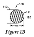
図1A及び1Bは、1つの実施形態による誘導センサ100の、それぞれ側面図及び断面図を例示する。誘導センサ100は、1つ以上のループ111を有し、インダクタンス値に関連するインダクタ110を包含する。インダクタのインダクタンス値Lは、一般に、インダクタコイルに結合する材料の透磁率、巻き数、インダクタの断面積、及びインダクタの長さの関数である。
1A and 1B illustrate side and cross-sectional views, respectively, of an
誘導センサ110は、センサ材料120の寸法変化によって検知パラメータの変化に応答するセンサ材料120を包含する。センサ材料120は、インダクタ110のループ111の中に、インダクタ110のループ111により画定された領域内に配向される。目的のパラメータの変化に暴露されたとき、センサ材料120は寸法変化を経験し(例えば、膨張する又は収縮する)、これは、インダクタ110のループ111により画定された領域の対応する寸法変化を生成する。
図1A及び1Bは、検知されているパラメータの変化前の初期条件での誘導センサ100の、それぞれ側面図及び上面図を例示する。誘導センサ100は、初期長さl0、初期直径w0、初期面積A0、及びコイルの各対の間の初期距離d0を包含する初期構成を有する。図1C及び1Dは、パラメータ変化に暴露後の誘導センサ100の側面図及び断面図を例示する。長さl1、直径w1、面積A1、又はループ111間の距離d1の1つ以上が、センサ材料120の膨張によって変化しており、インダクタループ111により画定される領域の対応する膨張を生じさせる。インダクタの長さ、直径、面積、又はループ間の距離のいずれかの1つ以上の変化は、インダクタのインダクタンス値の変化を生じさせる。
1A and 1B illustrate a side view and a top view, respectively, of the
センサ材料は、目的の検知パラメータの変化によって寸法変化を示すように選択される。例えば、センサ材料は1つ以上の軸に沿って膨張又は収縮して、センサ材料の幅、長さ、又は断面積の1つ以上の変化を生じさせる場合がある。1つの特に有用なセンサ材料は、本明細書においてpVA−pAAヒドロゲルと表示される、ポリ(ビニルアルコール)−ポリ(アクリル酸)ヒドロゲルのようなヒドロゲルを含み、それは、水分、pH、又は他のパラメータのような環境条件の変化によって寸法変化を経験する。 The sensor material is selected to exhibit a dimensional change due to a change in the desired sensing parameter. For example, the sensor material may expand or contract along one or more axes, causing one or more changes in the width, length, or cross-sectional area of the sensor material. One particularly useful sensor material includes a hydrogel, such as a poly (vinyl alcohol) -poly (acrylic acid) hydrogel, denoted herein as pVA-pAA hydrogel, which can be moisture, pH, or other Experience dimensional changes due to changes in environmental conditions such as parameters.
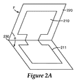
図2Aは、誘導センサの別の実施形態を例示する。この実施形態では、センサ材料は任意である。インダクタのループ210、211は、基材220の上に任意に形成されてもよく、ヒンジ230により結合される。ヒンジ230の操作は、ループ210、211間の角度θを変化して、ループ210、211間の距離の変化、及びインダクタのインダクタンスの対応する変化を生じさせる。ヒンジ230は、ループ210、211の1つ又は両方に直接的に又は間接的に適用される力Fに対抗するバネ又はその他の機構を包含してもよい。
FIG. 2A illustrates another embodiment of an inductive sensor. In this embodiment, the sensor material is optional. The
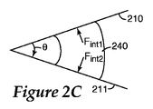
図2Bに例示されるように、一部の実施形態は、ループ210、211により形成された角度θの外側に配置されたセンサ材料240を利用する場合がある。センサ材料240の寸法変化は、力Fextをループ210、211の1つ又は両方の上に生成する。他の実施形態では、図2Cに例示されるように、センサ材料240は、ループ210、211により形成された角度θの内側に配置される場合がある。センサ材料240の寸法変化は、力Fint1、Fint2をループ210、211の1つ又は両方の上に生成する。
As illustrated in FIG. 2B, some embodiments may utilize
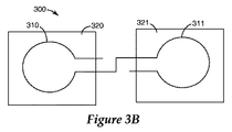
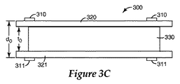
図3A〜3Dは、1つの実施形態による誘導センサ300について、ヒンジのない構成を例示する。図3Aは、基材320、321、及びループ310、311の配向後、並びに基材320、321間及びループ310、311間へのセンサ材料330の配置後の誘導センサを示す。図3Bは、基材320、321、及びセンサ材料のないループ310、311の電気的接続を例示する。
3A-3D illustrate a hingeless configuration for an
図3C及び3Dの断面図により更に例示されるように、誘導センサ300は、それぞれ、基材320、321上に形成された2つのループ310、311を包含する。センサ材料330は、ループ310、311間に配置される。センサ材料330は、t0の初期厚さを有し、ループ310、311間の距離d0を結果として生じる。センサ材料330は、特定の目的の検知パラメータに対して、寸法的に感応性である。検知パラメータの変化に従って、センサ材料330は、厚さt1まで膨張し、ループ310、311の間の距離d1を生成する。あるいは、一部の実施では、センサ材料330は、検知パラメータへの暴露後に初期厚さt0から収縮して、ループ310、311を共により近くにもたらす場合がある。
As further illustrated by the cross-sectional views of FIGS. 3C and 3D, the
図3Bに例示されるように、誘導センサ300は、上部及び下部ループ310、311の中を電流が同じ方向に流れる正型デバイスとして電気的に接続されてもよい。正型デバイスのループ310、311により生成される磁場は、加算的であり、ループ310、311の間に正の相互インダクタンスを生じさせる。正型デバイスの全体のインダクタンスは、ループ310、311がより接近するにつれて増加し、ループ310、311が離れるにつれて減少する。
As illustrated in FIG. 3B, the
あるいは、誘導センサは、負型デバイスとして電気的に接続されてもよい。負型デバイスの上部及び下部ループの中の電流は、反対の方向に流れる。この構成では、1つのループの中を流れる電流により生成された磁場は、反対のループの中を流れる電流により生成された磁場を弱める。磁場の相殺は、ループ間に負の相互インダクタンスを生成する。負型デバイスの全体のインダクタンスは、ループがより接近するにつれて減少し、ループが離れるにつれて増加する。 Alternatively, the inductive sensor may be electrically connected as a negative device. The current in the upper and lower loops of the negative device flows in the opposite direction. In this configuration, the magnetic field generated by the current flowing in one loop weakens the magnetic field generated by the current flowing in the opposite loop. Magnetic field cancellation creates a negative mutual inductance between the loops. The overall inductance of the negative device decreases as the loop gets closer and increases as the loop leaves.
図1〜3により例示されたセンサは、例えば、温度、水分、pH、流量、塩分、溶媒組成物、グルコース濃度、電界、光、及びイオン濃度のような多様な環境条件を検知するために使用されてもよい。 The sensors illustrated by FIGS. 1-3 are used to detect a variety of environmental conditions such as, for example, temperature, moisture, pH, flow rate, salinity, solvent composition, glucose concentration, electric field, light, and ion concentration. May be.
図4Aのグラフは、約200μmのリード直径、約6mmのコイル長、約6mmのコイル直径、及び約1.8μHの初期インダクタンスL0を有する20巻き銅コイルインダクタのインダクタンスの変化を例示する。インダクタは、ポリ(ビニルアルコール)−ポリ(アクリル酸)(pVA−pAA)ヒドロゲル中に浸漬されて、インダクタの銅線をヒドロゲルによりコーティングした。この構成を有するデバイスを使用し、pH及び水分レベルの検知を実証した。乾燥後、ヒドロゲルをコーティングされたインダクタは、脱イオン水中に定置され、図4Aに描かれるように、インダクタンスが経時的に測定された。 The graph of FIG. 4A illustrates the change in inductance of a 20-turn copper coil inductor having a lead diameter of about 200 μm, a coil length of about 6 mm, a coil diameter of about 6 mm, and an initial inductance L 0 of about 1.8 μH. The inductor was immersed in a poly (vinyl alcohol) -poly (acrylic acid) (pVA-pAA) hydrogel to coat the copper wire of the inductor with the hydrogel. Devices with this configuration were used to demonstrate pH and moisture level sensing. After drying, the hydrogel coated inductor was placed in deionized water and the inductance was measured over time as depicted in FIG. 4A.
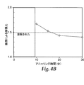
pVA−pAAヒドロゲルのいくつかの組成は、アニーリングなしで水に可溶性である。例えば、3重量%pVA及び6重量%PAAを有するヒドロゲルは、図4Bに示されるように、それが130℃で10分以上アニールされるとき不溶性になる。図4Bは、アニール時間とヒドロゲルの膨張比との間の依存関係を例示する。 Some compositions of pVA-pAA hydrogels are soluble in water without annealing. For example, a hydrogel with 3 wt% pVA and 6 wt% PAA becomes insoluble when it is annealed at 130 ° C. for more than 10 minutes, as shown in FIG. 4B. FIG. 4B illustrates the dependence between annealing time and hydrogel expansion ratio.
12重量%pVA及び1.5重量%pAAを有するヒドロゲルは、アニーリングなしで水に不溶性であることが観察された。図4Cのグラフは、pHの関数として、ヒドロゲルの2種類についての膨張/収縮曲線を例示する。曲線410及び411は、130℃で20分間アニールされた、3重量%pVA及び6重量%PAAを含むヒドロゲルのそれぞれ正規化された収縮及び膨張曲線を例示する。曲線420、421は、12重量%pVA及び1.5重量%pAAを含むヒドロゲルのそれぞれ正規化された収縮及び膨張曲線を例示する。膨張及び収縮曲線410、411、420、421において観察できるヒステリシスが、前の膨張又は収縮周期の検出を可能にするメモリとして使用されてもよい。
Hydrogels with 12 wt% pVA and 1.5 wt% pAA were observed to be insoluble in water without annealing. The graph of FIG. 4C illustrates the expansion / contraction curves for two types of hydrogels as a function of pH.
特定の実施形態では、誘導センサをコンデンサと結合し、共振タンク回路を形成してもよい。共振回路の共振周波数及び/又はその他の共振特性は、誘導センサのインダクタンスの関数として変化する。共振周波数及び/又はその他の共振特性の変化は、有線又は無線接続を介して共振回路に結合された検出回路(detector circuitry)を介して検出されてもよい。 In certain embodiments, an inductive sensor may be coupled with a capacitor to form a resonant tank circuit. The resonant frequency and / or other resonant characteristics of the resonant circuit varies as a function of the inductance of the inductive sensor. Changes in the resonant frequency and / or other resonant characteristics may be detected via detector circuitry coupled to the resonant circuit via a wired or wireless connection.
無線接続を通じた遠隔検知は、アクセスが困難な場所及び/又は低価格での適用において特に有用である。電子商品監視(EAS)又は無線周波数識別(RFID)技術は、目的の物品の存在を検出し、その動きを追跡するために使用されてきた。例えば、EAS及び/又はRFID技術は、書店又は図書館の本を検出及び追跡するために頻繁に使用される。本明細書で記載されるような誘電センサは、EAS又はRFID技術の遠隔アクセス能力による検知機能性と合わせて、共振回路の要素として使用されてもよい。 Remote sensing through a wireless connection is particularly useful in difficult to access and / or low cost applications. Electronic merchandise monitoring (EAS) or radio frequency identification (RFID) technology has been used to detect the presence of an object of interest and track its movement. For example, EAS and / or RFID technology is frequently used to detect and track books in a bookstore or library. A dielectric sensor as described herein may be used as an element of a resonant circuit in conjunction with sensing functionality due to the remote access capabilities of EAS or RFID technology.
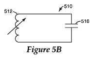
図5Aは、EAS/RFIDの適用のために使用される共振回路510を例示する回路図である。遠隔アクセスができるEAS/RFIDデバイスは、インダクタ512及びコンデンサ516を平行に含む単純回路510を使用してもよい。回路510は、回路構成要素512、516の値に依存する固有の周波数で共振するように設計される。インダクタ512は、無線周波数(RF)エネルギーのような電磁エネルギーを受信、反射、及び/又は送信するために使用されるアンテナとしての役割を果たす。一部の適用では、アンテナを介して識別コードを出力するために、追加の回路(示されず)を共振回路510に結合される。コードを送信できるデバイスは、典型的にはRFIDデバイスと称される。IDコードを出力するための追加の回路のないデバイスは、多くの場合EASデバイスと称される。EASデバイスは、読取装置により放出された、RF場のような電磁(EM)場を吸収し乱すように設計される。EM場の乱れは読取装置により検出されてもよく、EASデバイスは典型的には物品についての追加情報を送信できないが、EASデバイスの存在を示すと解釈されてもよい。
FIG. 5A is a circuit diagram illustrating a
本発明の実施形態により、EAS又はRFIDに基づく検知回路は、共振回路の構成要素として本明細書に記載されるような誘導センサを包含する。誘導センサは、1つ以上の目的のパラメータに対して感応性である。目的のパラメータの変化は、誘導センサのインダクタンス値の修正を生じさせる。共振回路のインダクタンスの変化は、共振回路の共振特性の対応する変化を生じさせる。様々な構成において、インダクタンスの変化により修正される共振特性としては、共振周波数、Qファクタ、帯域幅、及び/又は共振回路のその他の共振特性を挙げてもよい。 According to embodiments of the present invention, an EAS or RFID based sensing circuit includes an inductive sensor as described herein as a component of a resonant circuit. Inductive sensors are sensitive to one or more target parameters. The change in the target parameter causes a correction of the inductance value of the inductive sensor. A change in the inductance of the resonant circuit causes a corresponding change in the resonance characteristics of the resonant circuit. In various configurations, resonance characteristics that are modified by changes in inductance may include resonance frequency, Q factor, bandwidth, and / or other resonance characteristics of the resonance circuit.
図5Bの回路図は、誘導センサ522及びコンデンサ516を包含する共振回路/センサ520を例示する。誘導センサ522は、目的のパラメータに基づいてインダクタンス値を変えるように構成される。誘導センサ522のインダクタンス値の変動は、共振回路/センサ520の共振特性の変化を生じさせる。共振特性の変化は、遠隔検出され、RFID又はEAS読取装置(示されず)によって解釈されることができる。
The circuit diagram of FIG. 5B illustrates a resonant circuit / sensor 520 that includes an inductive sensor 522 and a
共振周波数、又はその他の共振特性の変化は、目的の検知パラメータの変化が起きたことを示すと解釈されることができる。一部の実施によると、回路520の共振周波数の変化は、検知パラメータの変化の量、程度、又は持続時間を決定すると解釈される。ある期間にわたって回路520の共振周波数(又は他の特性)の変化を検出することを使用し、検知パラメータの変化の進行を追跡してもよい。 A change in resonance frequency, or other resonance characteristic, can be interpreted to indicate that a change in the desired sensing parameter has occurred. According to some implementations, changes in the resonant frequency of circuit 520 are interpreted as determining the amount, extent, or duration of change in the sensing parameter. Detecting changes in the resonant frequency (or other characteristic) of the circuit 520 over a period of time may be used to track the progress of changes in the sensing parameter.
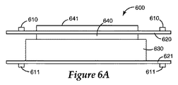
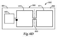
図6A〜6Eは、2つのコイルループを有しコンデンサと共に共振回路を形成する誘導センサの様々な実施形態を例示する。図6Aは、1つの実施形態による図6Bの断面A−A’で切り取られた共振回路/センサ600の断面図を例示する。誘導センサは、基材620、621上に配置された2つのループ610、611を包含する。コンデンサを形成する第1及び第2のプレート640、641は、基材620の1つの向かい合った側面上に配置される。センサ材料630の寸法変化が、ループ610、611間の距離の対応する変化を生じさせるように、目的のパラメータに対して寸法的に感応性であるセンサ材料630が、基材620、621間、又はループ610、611間に配置される。図6Bは、センサ材料のない、共振回路構成要素610、611、640、及び基材620、621を例示する。インダクタ及びコンデンサは電気的に接続されて、図5Bに例示される回路520のような共振回路を形成する。
6A-6E illustrate various embodiments of an inductive sensor that has two coil loops and forms a resonant circuit with a capacitor. FIG. 6A illustrates a cross-sectional view of a resonant circuit /
一部の実施形態では、図6C〜Eに例示されるように、インダクタのループ610、611、及びコンデンサプレート640は、第1及び第2の部分661、662を包含する単一の折り畳み式基材660上に形成されてもよい。基材660の第1及び第2の部分661、662は、屈曲ヒンジ部分650により分離されている。屈曲ヒンジ650の操作は、インダクタループ610、611が、互いに重なり合うように配向することを可能にする。寸法的に応答するセンサ材料(示されず)は、センサ材料の寸法変化がループを共により接近させる又はより遠く離れさせるように、ループ610、611に関して配向されてもよい。一部の実施形態は、穿孔670を採用し、基材部分661、662の間に挟まれている検知材料に被検質が到達するのを可能にする。
In some embodiments, as illustrated in FIGS. 6C-E, the
一体型コンデンサの1つ又は両方の電極640は、図6Cに例示されるように、区画642に分割されてもよい。コンデンサ電極640を区画642に分割することは、デバイス600と質問機の外部アンテナとの間の電磁結合を妨げる場合があるコンデンサ電極640中の渦電流を低減する。
One or both
図6D及び6Eは、折り畳み式基材660上に形成された共振回路として配列された誘導センサ及びコンデンサのための様々な構成を例示する。図6Dは、ループ610により囲まれた領域の外側の1つの基材部分661上に形成された、コンデンサプレート640を有する負型デバイスを例示する。基材660が、屈曲ヒンジ650のところで折り畳まれ、ループ610、611が重なり合うとき、上部610及び下部611ループ中の電流は反対の方向に流れ、ループ610、611中を流れる電流により生成された磁場の相殺によって負の相互インダクタンスを生成する。この負型デバイスの全体のインダクタンスは、上部及び下部ループ610、611が互いにより接近するにつれて減少し、ループ610、611がより遠く離れるにつれて増加する。
6D and 6E illustrate various configurations for inductive sensors and capacitors arranged as a resonant circuit formed on a
図6Eは、正型デバイスを例示する。基材660が、基材部分661、662、及びループ610、611が重なり合うように折り畳まれるとき、重なり合うループ610、611の中の電流は同じ方向に流れる。正型デバイスの全体のインダクタンスは、ループ610、611が共により接近するにつれて増加し、ループ610、611がより遠く離れるにつれて減少する。
FIG. 6E illustrates a positive device. When the
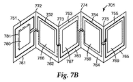
一部の実施形態では、誘導センサのインダクタは、図7A及び7Bに例示されるもののような複数のループを包含してもよい。追加のループの使用は、増加した公称インダクタンスを提供し、これは、センサと質問機との間により良好な誘導結合を実現するために有益である。図7Aは、単一の折り畳み式基材720の上に配置された複数の同心ループ710、711のあるインダクタを有する共振回路/センサを例示する。複数の同心ループ710、711は、それぞれ基材部分721、722上に形成される。基材720は、基材部分721、722間に屈曲ヒンジ部分791を包含する。折り畳まれたとき、ループ710、711は重なり合って複数ループのインダクタを形成する。コンデンサは、インダクタループ711により囲まれた領域内に配置された、分割された容量プレート740により1つの基材部分722上に形成される。基材部分721、722の1つ又は両方は、穿孔790を包含し、ループ710、711間に配置されたセンサ材料(示されず)の被検質又は検知されている他の周囲条件への暴露を可能にする。負若しくは正型インダクタ及び/又は共振回路の形成を実現するための適切な電気接続は、ビア相互接続795を使用して行われてもよい。
In some embodiments, the inductor of the inductive sensor may include multiple loops such as those illustrated in FIGS. 7A and 7B. The use of an additional loop provides increased nominal inductance, which is beneficial for achieving better inductive coupling between the sensor and the interrogator. FIG. 7A illustrates a resonant circuit / sensor having an inductor with a plurality of
図7Bに例示される、別の実施形態では、共振回路/センサ701は、5つの可撓性基材部分761〜765の上に形成された複数のループ751〜755を有するインダクタを包含する。各基材部分761〜765は、1つのループ751〜755をデバイス701のインダクタに提供する。ループ751〜755は、示されるように、すべてが基材部分761〜765の片側に、又は半分が基材部分761〜765の各側に形成されてもよい。基材部分761〜765は、デバイス701を、屈曲ヒンジ772〜775のところでジグザグ方式で折り畳むことにより積み重ねられ、基材部分の1つ761の上に形成されたプレート780、781を有するコンデンサと結合したソレノイド様インダクタを結果として生じる。容量プレート780、781を包含しない基材部分は、貫通孔766〜769を任意に有してもよい。
In another embodiment, illustrated in FIG. 7B, the resonant circuit /
一部の実施形態では、センサ材料(示されず)は、基材部分761〜765の1つ以上の間に配置される。基材部分761〜765が貫通孔766〜769を包含する場合、センサ材料は、基材部分761〜765の周辺部に沿って配置される。
In some embodiments, sensor material (not shown) is disposed between one or more of the substrate portions 761-765. When the
上記の誘導センサを介する遠隔検知は、誘導センサを組み込む共振回路に無線でアクセスできる質問機回路(interrogator circuitry)を使用して達成されてもよい。図8のブロック図は、本明細書においてまた読取装置としても表示される質問機830、及び誘導センサ812に結合されたコンデンサ826を有する共振回路820を包含する遠隔検知システム850を例示する。質問機830は、無線周波数(RF)源834及び共振分析器(resonance analyzer)836を包含する。
Remote sensing via the inductive sensor described above may be accomplished using interrogator circuitry that allows wireless access to the resonant circuit incorporating the inductive sensor. The block diagram of FIG. 8 illustrates a
質問機830は、アンテナ832を包含し、RF信号を共振回路820に送信する。共振回路820は、回路820の共振周波数に近いRFエネルギーを吸収及び反射する。質問機830は、共振回路820によるRFエネルギーの吸収及び/又は反射によって生じた送信された信号の変化を検出するように構成されてもよい。共振回路820によるエネルギーの吸収/反射に起因する質問機信号の変化、及び/又は共振回路820によリ反射された信号の検出は、本明細書では共振回路信号として表示される。
誘導センサ812は、センサ812のインダクタンス値を変更することにより、特定の目的のパラメータに応答するように設計される。共振回路820のインダクタンス値の変化は、回路820の共振周波数をシフトする。この周波数のシフトは、質問機830の共振分析器836によって検出可能である。
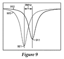
図9は、それぞれ時間t1及びt2において得られた周波数掃引からの質問機によって生成された信号910、920を示す。信号910、920は、共振回路/センサが質問機の付近に存在するときは、質問機により生成される。信号910は、時間t1において共振回路の初期共振周波数に関連する特徴911を包含する。信号920は、誘導センサのループ間の約200μmの増加後、時間t2において共振回路/センサの共振周波数に関連する信号の特徴921を示す。信号の特徴911、921の比較は、約3MHzの共振回路の共振周波数の下方シフトを示す。図10は、インダクタループ間の距離の関数としての共振周波数のグラフを示す。
FIG. 9 shows
センサ材料として前述のpVA−pAAヒドロゲルのようなヒドロゲルを使用するセンサは、水分吸収及び/又はpHの無線モニタリングを可能にする。図11Aは、デバイスを濡らした後の時間の関数としての共振周波数のグラフを示す。センサ材料により水分が吸収されるにつれて、センサの共振周波数は下方にシフトする。図11Aに示される結果は、吸収の最終的な飽和を示す。図11Bのグラフは、誘導センサ中に使用されるヒドロゲルセンサ材料の1つの特定の処方について、変化するpHによる共振回路の周波数の変化を例示する。 Sensors using hydrogels such as the aforementioned pVA-pAA hydrogel as sensor material allow for moisture absorption and / or wireless monitoring of pH. FIG. 11A shows a graph of resonant frequency as a function of time after wetting the device. As moisture is absorbed by the sensor material, the resonant frequency of the sensor shifts downward. The results shown in FIG. 11A show the final saturation of absorption. The graph of FIG. 11B illustrates the change in frequency of the resonant circuit with varying pH for one particular formulation of the hydrogel sensor material used in the inductive sensor.
一部の実施では、複数の誘導センサは同時にモニターされてもよい。例えば、誘導センサは、センサの無線モニタリングを促進するために異なる共振周波数を有する共振回路の中に組み込まれてもよい。複数のセンサは、異なる検知パラメータに又は同じ検知パラメータに応答するように構成されてもよい。一部の実施形態では、誘導センサは、目的の面積にわたって空間的に分布されてもよい。センサは、目的の面積にわたる1つ以上の検知パラメータの変化について、情報を獲得するようにモニターされることができる。無線でアクセス可能な空間的に分布されたセンサの使用は、その態様が本明細書に開示される誘導センサと併せて使用されてもよく、本明細書に参考として組み込まれる、同一所有者の米国特許出願番号第11/383652号(2006年5月16日出願)に記載されている。 In some implementations, multiple inductive sensors may be monitored simultaneously. For example, inductive sensors may be incorporated into resonant circuits having different resonant frequencies to facilitate wireless monitoring of the sensor. The plurality of sensors may be configured to respond to different detection parameters or to the same detection parameter. In some embodiments, the inductive sensors may be spatially distributed over the area of interest. The sensor can be monitored to acquire information about changes in one or more sensing parameters over the area of interest. The use of wirelessly accessible spatially distributed sensors may be used in conjunction with inductive sensors whose aspects are disclosed herein and are incorporated by reference herein. US patent application Ser. No. 11 / 383,652 (filed May 16, 2006).
一部の実施では、本明細書に記載されるように誘導センサを組み込む共振回路により生成された信号は、検知回路と質問機との間の誘導結合、及び/又は回路の電気的特性に影響する様々な条件により変更される場合がある。例えば、センサ信号は、目的の検知パラメータ以外の要因、例えば、質問機からのセンサ回路の配向及び/若しくは距離、電磁干渉、近くの金属物質、センサ回路と質問機との間に置かれた物質、温度変化、濡れ若しくは近くの水、並びに/又はその他の要因により影響される場合がある。 In some implementations, a signal generated by a resonant circuit incorporating an inductive sensor as described herein may affect inductive coupling between the sensing circuit and the interrogator and / or the electrical characteristics of the circuit. It may be changed according to various conditions. For example, the sensor signal may be a factor other than the desired sensing parameter, eg, orientation and / or distance of the sensor circuit from the interrogator, electromagnetic interference, nearby metal material, material placed between the sensor circuit and the interrogator , Temperature changes, wetting or nearby water, and / or other factors.
リファレンス信号は、上記の干渉源によるセンサ回路信号の測定値間の変動の説明をするために使用されてもよい。1つの実施形態では、検知回路によって生成された信号は、リファレンス信号に基づいて配向及び/又は距離について正規化されてもよい。干渉が、良質な測定の要件を超える場合には、アラーム状態が開始されてもよい。 The reference signal may be used to account for variations between measured values of the sensor circuit signal due to the interference sources described above. In one embodiment, the signal generated by the sensing circuit may be normalized for orientation and / or distance based on the reference signal. An alarm condition may be initiated if the interference exceeds the requirements of good quality measurements.
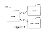
図12は、遠隔検知システム1200を例示する。検知システム1200は、質問機1210に無線で結合される検知回路1220及びリファレンス回路1230を包含する。検知回路1220の共振周波数のシフトは、リファレンス回路1230により生成された信号を使用して、質問機1210により解釈されてもよい。
FIG. 12 illustrates a
ここで図13Aを見ると、リファレンス回路1330及びセンサ回路1320は共振回路を含み、一部の実施形態による無線アクセスを提供してもよい。リファレンス回路1330は、センサ回路1320の共振周波数とは異なる共振周波数を有する。この構成では、リファレンス回路信号及びセンサ回路信号の両方が、質問機アンテナ1311を介して質問機1310により遠隔検出されることができる。リファレンス回路1330は、誘導センサデバイス1320のインダクタに類似するインダクタを採用してもよいが、インダクタループ間に固定空隙を有するか、又はデバイスを折り畳まないままにする。リファレンス回路1330によって生成された信号を使用して、上記の干渉源により生成される誤りを包含するセンサ回路信号の誤りを訂正してもよい。
Turning now to FIG. 13A, the
図13Bは、質問機1310により検出された、センサ及びリファレンス回路1320、1330の共振回路信号を示す。図13Bは、それぞれ、時間t1及びt2において質問機1310による周波数スキャンに応答する検知回路1320及びリファレンス回路1330により生成された信号1350、1360を描く。時間t1における信号1350は、センサ回路1320により生成され、またセンサ回路1320の初期共振周波数に関連する信号の特徴1351を包含する。時間t2における信号1360は、センサ回路1320により生成され、また目的の検知パラメータの変化後のセンサ回路1320の共振周波数に関連する信号の特徴1361を包含する。信号1350、1360の比較は、検知条件により検知回路1320により生成された、信号の特徴1351、1361の周波数のシフトを示す。信号1350及び1360はまた、それぞれ、時間t1及びt2において、リファレンス回路1330により生成された信号の特徴1370、1371も示す。これらの信号の特徴1370、1371は、実質的に変化しないままであるリファレンス回路1330の共振周波数に関連する。本実施例は、検知条件への暴露により生じた共振周波数の下方シフトを描くが、その他の構成では、検知条件への暴露は共振周波数の上方シフトを生じさせる場合もあることは理解されるだろう。
FIG. 13B shows the resonance circuit signals of the sensor and
図13Bに例示されたグラフでは、リファレンス回路の共振周波数は、時間t1及びt2において同じままであり、センサ回路信号が干渉により影響を受けない可能性があることを表す。経時的なリファレンス回路の共振周波数の変化は、センサ信号の補正が必要である場合があることを示す。 In the graph illustrated in FIG. 13B, the resonant frequency of the reference circuit remains the same at times t 1 and t 2 , indicating that the sensor circuit signal may not be affected by interference. A change in the resonant frequency of the reference circuit over time indicates that the sensor signal may need to be corrected.
遠隔検知のためのリファレンス信号の使用に関する更なる詳細は、本明細書に参考として組み込まれる、同一所有者の米国特許出願番号11/383652号(2006年5月16日出願)に記載されている。 Further details regarding the use of reference signals for remote sensing are described in commonly owned US patent application Ser. No. 11 / 383,652, filed May 16, 2006, which is incorporated herein by reference. .
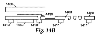
1つの実施形態により、共振センサ回路を作製するためのプロセスが、図14A〜Cに描かれる。図14Aは、折り畳まれていないセンサの平面図を例示する。図14Bは、断面B−B’を通って切り取られたセンサの断面図を例示する。それぞれ、図14A及び14Bの平面図及び断面図において例示されるように、一体型コンデンサを有する2重ループインダクタのための適切なパターンが、ポリイミド−銅(PI−Cu)ホイルのような平面可撓性基材1420上に形成される。インダクタループ1410、1411は、第1のループ1410の1つの端が第2のループ1411のもう1つの端に接続されるように形成される。ヒンジは、PI−Cu基材1420の薄くされた部分1450によってループ1410、1411間に形成される。ヒドロゲルのようなセンサ材料1430は、第1及び第2のループに関して配向される。穿孔1480をPI−Cu基材1420を通して任意に形成し、被検質又は目的の周囲条件へのセンサ材料1430の暴露を可能にしてもよい。1つ以上のビア接続1490が、基材1420を通しての電気的接続を促進するために使用される。誘導センサの2重ループ構造は、図14Cの矢印により例示されるように、薄くされたヒンジ1450のところで、平面基材1420を折り畳むことにより実現される。センサ材料1430の寸法変化は、ループ1410、1411間の隙間距離、及び回路のインダクタンスを変化させる。図14A〜Cに例示される構成は、標準的なリソグラフィーに基づくプロセスを使用して誘導センサの製作を可能にするデバイス構造を提供する。
According to one embodiment, a process for making a resonant sensor circuit is depicted in FIGS. FIG. 14A illustrates a plan view of an unfolded sensor. FIG. 14B illustrates a cross-sectional view of the sensor taken through section B-B ′. A suitable pattern for a double loop inductor with an integral capacitor is shown in FIG. 14A and 14B in plan and cross-sectional views, respectively, such as a polyimide-copper (PI-Cu) foil. Formed on a
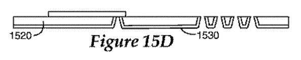
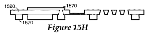
図15A〜Hは、本発明の実施形態による、誘導センサ及び共振回路の製作のための代表的なプロセスをより詳細に例示する。図15A〜Hに示されるプロセスを使用して、誘導センサ及び共振回路は、ポリイミド−銅フィルム及びフォトリソグラフィーに基づく技術を使用してバッチ製作されてもよいが、フォトリソグラフィー以外の技術及び/又は代替材料があるいは使用されてもよい。図15A〜Hは、1つのセンサデバイスの製作プロセスを例示する。以下に記載される技術を使用して、複数のデバイスが、デバイスを分離するために後で切断される一体型基材上に製作されてもよい。 15A-H illustrate in greater detail an exemplary process for the fabrication of inductive sensors and resonant circuits, according to embodiments of the present invention. Using the process shown in FIGS. 15A-H, inductive sensors and resonant circuits may be batch fabricated using polyimide-copper film and photolithography-based techniques, but technologies other than photolithography and / or Alternative materials may alternatively be used. 15A-H illustrate the fabrication process of one sensor device. Using the techniques described below, multiple devices may be fabricated on an integral substrate that is later cut to separate the devices.
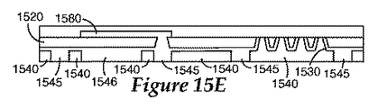
第1のマスクを使用して、厚さ50μmのPIホイル1520上にコーティングされた厚さ15μmのCuフィルム1510をパターン化し、平行プレートコンデンサの電極1580を形成する(図15A及び15B)。流体被検質用通路としての役割を果す貫通孔1590、並びに回路のためのビア接続用の孔1595が、ポリイミド(PI)基材1520の中に製作される(図15C)。貫通孔1590及び/又はビア接続孔1595の形成は、例えば40重量%KOH及び20重量%エタノールアミンを有する水溶液中での湿式エッチングにより実現されてもよい。エタノールアミンの使用はエッチングされた孔の中のテーパーリングを低減し、これは検知要素がより容易に被検質に暴露される広い開口部面積を得られるようにする。図15Dに例示されるように、シード層1530は、図15Eに記載される電気メッキプロセスにおいて使用するために、PI基材1520上にコーティングされる。シード層1530は、約100nmのチタンフィルムを接着層として堆積し、次いで約1μmのCuフィルムを堆積することにより形成される。シード層1530の銅表面上に積層されたポリメチルメタクリレート(PMMA)フォトレジストフィルム1540はパターン化されて、インダクタループ1545のCuメッキ、第2のコンデンサ電極1546、及びビア相互接続1591のための成形ダイを形成する(図15E)。より厚いループは、より大きいインダクタンス及びより小さい抵抗、即ちより高い品質要因を提供する。約50μmの厚さを有するフォトレジストを使用し、Cuメッキから40μmの目標高さを実現する。Cuメッキは、平滑化添加剤及び光沢添加剤を有する硫酸に基づく浴の中で実行される。Ti/Cuシード層1530を、メッキ後エッチングし、メッキ構造1545、1546、1591を電気的に分離する(図15F)。
Using a first mask, a 15 μm
PI 1520を再びエッチングし、屈曲ヒンジを形成する薄くされた部分1521を作製する(図15G)。KOHに基づくエッチング装置の中で2分間エッチングすると、薄くされた部分1521におけるPI 1520に厚さ10μmをもたらす。最後に、厚さ約1μmのパリレン−CTM(Parylene-CTM)の共形の誘電体フィルム1570が、電気的保護のために、デバイスの全表面にわたってコーティングされる(図15H)。
前述のように、上に詳細に説明されたプロセスを使用し、誘導センサを形成するために使用された多数の平面デバイスを包含する固体フィルムを同時に形成してもよい。個々のデバイスは、例えば、ブレード又は他の分離技術を使用して固体フィルムから切断されてもよい。 As described above, the process described in detail above may be used to simultaneously form a solid film that includes a number of planar devices used to form an inductive sensor. Individual devices may be cut from the solid film using, for example, a blade or other separation technique.
個々のデバイスを折り畳み、インダクタループを、それらが重なり合うように配向する。寸法的に感応性であるセンサ材料が、向かい合う基材部分及び/又はループ内に、折り畳み前又は後のいずれかにおいて任意に配置される。適切なセンサ材料を選択することにより、デバイスを使用して多様なパラメータについての検知を実行することが可能である。例えば、pVA−pAA、ポリ(AA−アクリル酸イソオクチル(IOA))、及びポリ(ヒドロキシエチルメタクリレート(HEMA)−AA)のようなヒドロゲルが、それらの雰囲気のpHに依存して膨潤/収縮する。ポリ(3−スルホプロピルメタクリレート(SPMA)−IOA)及びpAAに基づくヒドロゲルのいくつかは、塩の濃度に応答する。ポリ(N−イソプロピルアクリルアミド)(pNIPPAm)は、温度に応答するポリマーの例である。フェニルボロン酸に基づくヒドロゲルの寸法変化は、グルコースの濃度と相関させることができる。 The individual devices are folded and the inductor loops are oriented so that they overlap. A dimensionally sensitive sensor material is optionally placed in the facing substrate portion and / or loop, either before or after folding. By selecting the appropriate sensor material, it is possible to perform sensing for various parameters using the device. For example, hydrogels such as pVA-pAA, poly (AA-isooctyl acrylate (IOA)), and poly (hydroxyethyl methacrylate (HEMA) -AA) swell / shrink depending on the pH of their atmosphere. Some of the hydrogels based on poly (3-sulfopropyl methacrylate (SPMA) -IOA) and pAA respond to salt concentration. Poly (N-isopropylacrylamide) (pNIPPAm) is an example of a polymer that responds to temperature. Hydrogel dimensional changes based on phenylboronic acid can be correlated with glucose concentration.
複数の化学的/物理的/生物学的パラメータの検知は、異なるセンサ材料を組み込む複数のセンサデバイスを使用することにより実施されることができる。例えば、pH及び塩分の同時モニタリングは、それぞれ、pVA−pAA及びポリ(SPMA−IOA)を、異なる共振周波数を有する2つの別個のデバイスと併せて使用することにより実施されることができる。デバイスは、これは例えばモニターされる目標液体の中に定置されてよく、遠隔質問機を通じて無線により質問され、2つのパラメータについての情報を提供することができる。 Detection of multiple chemical / physical / biological parameters can be performed by using multiple sensor devices that incorporate different sensor materials. For example, simultaneous pH and salinity monitoring can be performed by using pVA-pAA and poly (SPMA-IOA), respectively, in conjunction with two separate devices having different resonant frequencies. The device can be placed, for example, in the target liquid to be monitored, and can be interrogated wirelessly through a remote interrogator to provide information about two parameters.
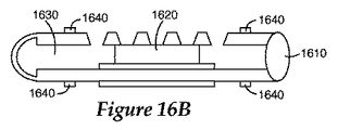
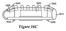
上記のプロセスを使用して製作された誘導センサは、折り畳み後誘導センサを初期構成に固定するように構成された機構を包含してもよい。図16A〜Cは、センサを固定するための機構を包含する1つの実施形態を例示している。センサは、図15A〜Hに関連して、上記のプロセスを使用して形成されてもよい。図16Aは、PI基材の薄くされた部分により形成されたヒンジの屈曲に続いて、初期条件にあるセンサを例示する。ヒンジの反対側の基材の末端部は、シリコンゴムのような柔軟な弾性結合材1610により結合されてもよい。シリコンゴムは、初期構成にある誘導センサを安定させる。図16Bは、目的のパラメータ、例えば被検質への暴露前の初期状態にある誘導センサを示す。乾燥したヒドロゲルの1片1620が、インダクタループ1640間の空隙1630内に配置される。ヒドロゲル1620は、被検質への暴露前に水和される。被検質又は周囲条件への暴露は、図16Cに例示されるように、ヒドロゲル1620を膨潤させるか又は膨潤を解消させ(de-swell)、インダクタループ1640間の距離を変化させる。図16Cの点線は、被検質への暴露前のデバイスの上部の構成を示す。図16Cの実線は、被検質への暴露による膨潤後のデバイスの上部の構成を示す。
An inductive sensor fabricated using the above process may include a mechanism configured to secure the inductive sensor in an initial configuration after folding. 16A-C illustrate one embodiment that includes a mechanism for securing the sensor. The sensor may be formed using the process described above in connection with FIGS. FIG. 16A illustrates the sensor in an initial condition following bending of the hinge formed by the thinned portion of the PI substrate. The end of the substrate opposite the hinge may be joined by a flexible
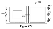
一部の実施形態では、センサを掛合することは、デバイスを初期構成に固定するために係合する相補的特徴を有するラッチング機構を使用して達成される。例えば、相補的特徴は、基材の末端部又は縁部上に配置されてもよい。1つの実施形態では、相補的特徴は、他の場所も可能であるが、ヒンジの反対側の基材の末端部上に配置される。図17Aは、折り畳み前の誘導センサ1700を描く。誘導センサ1700は、基材の1つの末端部に1つ以上のフック1710を包含する。フック1710は、基材の反対側の末端部で1つ以上のスリット1711と係合するように構成される。フック1710とスリット1711との係合は、図17Bに例示されるように、誘導センサを初期構成に掛合する。図15A〜Hに関連して記載されたリソグラフィーに基づく製作は、マスクレイアウトを修正することにより、単純なパターンから複雑なパターンまでを有するラッチング構造の追加を可能にする。
In some embodiments, engaging the sensor is accomplished using a latching mechanism having complementary features that engage to secure the device in the initial configuration. For example, complementary features may be placed on the ends or edges of the substrate. In one embodiment, the complementary feature is located on the end of the substrate opposite the hinge, although other locations are possible. FIG. 17A depicts the
図4Bに関連して前述されたように、特定の組成を有するpVA−pAAヒドロゲルは水中で可溶性であり、アニーリング後にのみ不溶性になることが見出された。溶解度特性を、誘導センサの組み立てにおいて利用することができる。図18A〜Dは、こうした手法の実施例を例示する。この実施形態では、可溶性ヒドロゲルの1片1810が、基材の向かい合う部分1821、1822の間の空隙の中に定置される。基材の向かい合う部分1821、1822の1つ又は両方の中に製作された孔1830は、センサ材料1810の水分への暴露を提供する(図18A)。
As described above in connection with FIG. 4B, it was found that pVA-pAA hydrogels with a specific composition are soluble in water and become insoluble only after annealing. Solubility characteristics can be exploited in the assembly of inductive sensors. 18A-D illustrate an example of such an approach. In this embodiment, a piece of
図18Bに例示されるように、ヒドロゲル1810の表面を孔1830を介して水1831で湿らせることは、ヒドロゲル1810の湿らされた領域を溶解し柔軟化させる。溶解されたヒドロゲル1810が乾く間に圧力1832を適用することにより、ヒドロゲル1810は、孔1830の中に押し出され、固化されたヒドロゲル1810と基材の向かい合う部分1821、1822との間の物理的結合を実現する。デバイスはアニールされてヒドロゲル1810を不溶性にする。図18Cは、アニーリング後のデバイスを例示する。
As illustrated in FIG. 18B, wetting the surface of
図18Dに例示された誘導センサは、基材部分1821、1822のより大きい変位1862を得るために、ヒドロゲルの変位1861を増幅する、てこの機構を提供するように、センサ材料1810がヒンジ1850及び基材部分1821、1822に関して配向される構造を例示する。基材部分1821、1822のより大きい変位1862は、いずれの機械的な増幅もないデバイスと比較したときに、デバイスのインダクタンス値のより大きい変化及び対応するより大きい信号を生成する。
The inductive sensor illustrated in FIG. 18D provides a lever mechanism that amplifies the
別の実施形態によって誘導センサを作製するためのプロセスは、多重ループデバイス(multi-loop device)を液体センサ材料によってコーティングすること、及びそれを乾燥させることを伴う。例えば、液体ヒドロゲル、又は液体形態の他のセンサ材料が、図7Bに例示される折り畳まれた多層デバイスのような多重ループデバイスの上にコーティングされてもよい。ヒドロゲルの粘度は、材料が折り畳まれた層の間の隙間に流れ込むことを可能にする。ヒドロゲルは次に乾燥される。アニーリングは、使用されるセンサ材料に依存して任意である。結果として生じるデバイスは、図19に例示される。センサ材料1920は、1つ以上のヒンジ1950で折り畳まれた基材1930上に配置されたループ1910の間に配置される。センサ材料1920は、周囲条件又は被検質への暴露に基づいて膨張及び収縮する。センサ材料1920の膨張又は収縮は、誘導ループ1910間の距離の変化を生じさせる。
A process for making an inductive sensor according to another embodiment involves coating a multi-loop device with a liquid sensor material and drying it. For example, a liquid hydrogel, or other sensor material in liquid form, may be coated over a multi-loop device, such as a folded multilayer device illustrated in FIG. 7B. The viscosity of the hydrogel allows the material to flow into the gaps between the folded layers. The hydrogel is then dried. Annealing is optional depending on the sensor material used. The resulting device is illustrated in FIG.
本明細書で記載された誘導センサについて多数の適用が想像されてもよい。1つの実施例では、誘導センサを創傷包帯又はおむつの中に採用し、創傷包帯又はおむつの水分含量を決定することができる。これらの製品について、包帯を取り外さずに、包帯又はおむつが水分の限界に到達したかどうかを決定することができることは有利である。創傷包帯又はおむつの取り替えの時間を適切に計ることは、ユーザーが不快な又は有害な条件を経験する可能性を低減する。包帯又はおむつの水分含量は、本明細書に記載されたような誘導センサを有する共振回路を組み込むデバイスを使用して遠隔でモニターされてもよい。デバイスは、バッチ方式で製作されることができ、電池のような内部電源を必要としない。これらの要因は、デバイスのコストを低減し、デバイスを使い捨て製品の中に組み込むことを実際的にする。 Numerous applications may be envisioned for the inductive sensors described herein. In one example, an inductive sensor can be employed in a wound dressing or diaper to determine the moisture content of the wound dressing or diaper. For these products, it is advantageous to be able to determine whether the bandage or diaper has reached its moisture limit without removing the bandage. Proper timing of wound dressing or diaper replacement reduces the likelihood that a user will experience unpleasant or harmful conditions. The moisture content of the bandage or diaper may be monitored remotely using a device that incorporates a resonant circuit with an inductive sensor as described herein. The device can be fabricated in a batch mode and does not require an internal power source such as a battery. These factors reduce the cost of the device and make it practical to incorporate the device into a disposable product.
図20は、誘導センサ2001を組み込む創傷包帯2000を例示する。包帯2000は、負傷した領域2020の上への定置のために構成された吸収性材料2010を包含する。創傷包帯2000は、通気性保護フィルム2030により覆われる。創傷包帯2000はまた、本明細書に記載されるように誘導センサを組み込む共振回路を有する水分センサ2001も包含する。一部の実施形態では、水分センサ2001は、包帯2000の吸収性材料2010の上又は近くに定置されてよい。他の実施形態では、図20に例示されるように、吸収性材料2010は、誘導センサのセンサ材料として使用されてもよい。吸収性材料2010が水分を吸収するにつれて、誘導センサ2001の吸収性材料2010は膨張し、センサ2001のインダクタンスの変化及び共振回路の共振周波数の対応する変化を生じさせる。共振周波数の変化は、遠隔質問機により無線で検出されてもよい。質問機又は他の回路は、水分限界に到達したときには警告を発生して、包帯を替えるべきであることを表す場合がある。前述のように、質問機は、複数のパラメータを検知するために異なる初期共振周波数を有するように製作された複数のセンサをモニターしてもよい。複数センサの使用は、複数パラメータの同時検知を可能にする。代替的に、又は追加的に、複数のセンサを使用し、参照としてセンサの1つ以上を使用して補正を提供する。
FIG. 20 illustrates a wound dressing 2000 that incorporates an
前述のように、一部の実施形態によると、誘導センサはインダクタの寸法を変化させるためにセンサ材料を使用する必要はない。誘導ループ間の間隔の変化は、ループの1つ又は両方の上に発揮された圧力により生じてもよい。寸法的に感応性である物質を組み込まない誘導センサの使用が、次の2つの適用実施例に記載される。 As mentioned above, according to some embodiments, the inductive sensor does not need to use sensor material to change the dimensions of the inductor. The change in spacing between the induction loops may be caused by pressure exerted on one or both of the loops. The use of inductive sensors that do not incorporate dimensionally sensitive materials is described in the following two application examples.
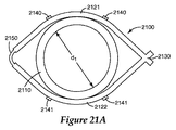
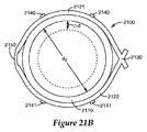
ヒンジで連結された誘導センサは、流量のようなパラメータの無線モニタリングのために使用されてもよい。1つの実施例は、図21A〜Bに例示されるが、誘導センサ2100を使用し、可撓性チューブ2110を通過する液体(例えば、血液)の脈動流を測定する。この適用では、チューブ2110は、検知デバイス2100の第1及び第2の基材部分2121、2122によって、ゆるく挟まれている。図21A〜Bに描かれる検知デバイス2120は、ラッチング機構2130及びデバイス2100のチューブ2110の周囲への固定を促進するヒンジ2150を包含する。チューブ2110の直径の変化は、誘導ループ2140、2141間の距離の変化を生じさせる。液体の脈動流は、チューブ2110の直径及びデバイス2100の共振周波数の周期的な変化を生じさせる。図21Aは、チューブ2110が最初の直径d1を有する時間t1におけるデバイス2100を例示している。図21Bは、チューブ2110が直径d2を有する時間t2におけるデバイス2120を例示している。チューブ2110の直径の変化Δdは、センサデバイス2100の共振周波数のシフトを生じさせる。チューブ直径の周期的変化に対応する共振周波数の周期的変化の頻度を測定することにより、流速が決定されてもよい。
A hinged inductive sensor may be used for wireless monitoring of parameters such as flow rate. One example, illustrated in FIGS. 21A-B, uses an
更に別の代表的な適用では、図22に示されるが、センサデバイス2210を使用し、チャネル2200の中の流量を測定する。センサデバイス2210はヒンジを包含し、1つの基材部分2202が初期角度θ0で、もう1つの基材部分2201に関して配向されるように、初めに折り畳まれる。1つの基材部分2202は、流体チャネル2200の内壁2230上に固定される。2つの基材部分2201、2202間の角度は、自由な基材部分2201が、流量により生じた圧力のために下方に押されるのにつれて減少する。より小さい流速は、基材部分2201、2202の初期配向に関して、相対的により小さい角度の変位θ1を生成する。より大きい流速は、基材部分2201、2202の初期配向に関して、相対的により大きい角度の変位θ2を生成する。基材部分2201、2202間の角度の変位の変化は、センサのインダクタンスを変更し、共振周波数のシフトを生じさせる。共振周波数のシフトは、遠隔質問機により無線でアクセスされ、チャネル中の流速に相関されてもよい。
In yet another exemplary application, as shown in FIG. 22, a
本発明の様々な実施形態についての上述の説明は、例示及び説明を目的として提示されている。それは、包括的であることも、又は開示されたまさにその形態に本発明を限定することも意図していない。以上の教示を考慮すれば、多くの修正及び変形が可能である。例えば、本発明の実施形態は、多種多様な適用において実施されてもよい。本発明の範囲は、この「発明を実施するための形態」によって限定されず、むしろ添付「特許請求の範囲」によって限定されるものとする。 The foregoing descriptions of various embodiments of the present invention have been presented for purposes of illustration and description. It is not intended to be exhaustive or to limit the invention to the precise form disclosed. Many modifications and variations are possible in view of the above teachings. For example, embodiments of the present invention may be implemented in a wide variety of applications. It is intended that the scope of the invention be limited not by this "DETAILED DESCRIPTION", but rather by the appended claims.
本発明は様々な修正及び代替形態に柔軟に従うことができるが、それらの細目は一例として図面に示され詳細に記述される。しかしながら、記載された特定の実施形態に本発明を限定することを意図しないことは理解されよう。逆に、添付の特許請求の範囲で定義された本発明の範囲内に入るすべての修正、等価物、及び代替物を含むことを意図している。 While the invention is amenable to various modifications and alternative forms, specifics thereof have been shown by way of example in the drawings and will be described in detail. It will be understood, however, that the intention is not to limit the invention to the particular embodiments described. On the contrary, the intention is to cover all modifications, equivalents, and alternatives falling within the scope of the invention as defined by the appended claims.
Claims (20)
1つ以上のループを含み、インダクタンスと関連するインダクタと、
センサ材料であって、前記センサ材料が前記センサ材料の寸法変化によって目的のパラメータに応答するように構成され、前記センサ材料の前記寸法変化が前記インダクタの寸法変化を生成するように、前記センサ材料が前記インダクタの前記ループ内に配向され、前記インダクタの前記寸法変化が前記インダクタの前記インダクタンスを変更する、センサ材料と、を含む、センサ。 An inductive sensor,
An inductor including one or more loops and associated with an inductance;
A sensor material, wherein the sensor material is configured to respond to a target parameter by a dimensional change of the sensor material, and the dimensional change of the sensor material generates a dimensional change of the inductor. Is oriented in the loop of the inductor, and the dimensional change of the inductor modifies the inductance of the inductor.
1つ以上のループを含むインダクタと、
センサ材料であって、前記センサ材料の寸法変化によって目的のパラメータに応答するように構成され、前記センサ材料の前記寸法変化が前記インダクタの寸法変化を生成して、前記インダクタのインダクタンスの変化を生じさせるように、前記インダクタの前記ループにより画定される領域内に配向されるセンサ材料と、
前記インダクタに電気的に結合されて前記インダクタンスに依存する共振特性を有する共振回路を形成するセンサ回路と、を含む誘導センサと、
前記共振回路の前記共振特性の変化を検出するように、及び前記共振特性に基づいて前記目的のパラメータを分析するように構成される質問機と、を含む、システム。 A sensor system,
An inductor including one or more loops;
A sensor material configured to respond to a target parameter by a dimensional change of the sensor material, wherein the dimensional change of the sensor material generates a dimensional change of the inductor, resulting in a change in inductance of the inductor; A sensor material oriented in a region defined by the loop of the inductor,
An inductive sensor comprising: a sensor circuit that is electrically coupled to the inductor and forms a resonant circuit having a resonant characteristic that depends on the inductance;
An interrogator configured to detect a change in the resonance characteristic of the resonance circuit and to analyze the target parameter based on the resonance characteristic.
前記目的のパラメータが水分を含み、
前記質問機が、前記誘導センサの前記共振特性に基づいて前記包帯中の水分を検出するように構成されている、請求項16に記載のセンサシステム。 The inductive sensor is disposed in or on a moisture-absorbing bandage configured to be placed on a patient;
The parameter of interest includes moisture;
The sensor system of claim 16, wherein the interrogator is configured to detect moisture in the bandage based on the resonance characteristics of the inductive sensor.
Applications Claiming Priority (2)
| Application Number | Priority Date | Filing Date | Title |
|---|---|---|---|
| US11/456,410 US20080018424A1 (en) | 2006-07-10 | 2006-07-10 | Inductive sensor |
| PCT/US2007/072475 WO2008008643A2 (en) | 2006-07-10 | 2007-06-29 | Inductive sensor |
Publications (2)
| Publication Number | Publication Date |
|---|---|
| JP2009544009A true JP2009544009A (en) | 2009-12-10 |
| JP2009544009A5 JP2009544009A5 (en) | 2010-08-12 |
Family
ID=38924022
Family Applications (1)
| Application Number | Title | Priority Date | Filing Date |
|---|---|---|---|
| JP2009519581A Pending JP2009544009A (en) | 2006-07-10 | 2007-06-29 | Inductive sensor |
Country Status (5)
| Country | Link |
|---|---|
| US (1) | US20080018424A1 (en) |
| EP (1) | EP2041760A2 (en) |
| JP (1) | JP2009544009A (en) |
| CN (1) | CN101496121A (en) |
| WO (1) | WO2008008643A2 (en) |
Cited By (3)
| Publication number | Priority date | Publication date | Assignee | Title |
|---|---|---|---|---|
| KR20200061510A (en) * | 2018-11-25 | 2020-06-03 | 주식회사 큐유아이 | Detection device and reader for measuring the amount of water content in building structures |
| JP2021512724A (en) * | 2018-02-09 | 2021-05-20 | スリーエム イノベイティブ プロパティズ カンパニー | Fall protection with guidance sensor for connection status and control |
| WO2022215220A1 (en) * | 2021-04-08 | 2022-10-13 | 日本電信電話株式会社 | Resonance circuit |
Families Citing this family (19)
| Publication number | Priority date | Publication date | Assignee | Title |
|---|---|---|---|---|
| US7948380B2 (en) * | 2006-09-06 | 2011-05-24 | 3M Innovative Properties Company | Spatially distributed remote sensor |
| DE102007043443B4 (en) * | 2007-09-12 | 2009-06-10 | Siemens Ag | Method for producing a curved coil and associated winding plate |
| WO2009081683A1 (en) * | 2007-12-26 | 2009-07-02 | Murata Manufacturing Co., Ltd. | Antenna apparatus and wireless ic device |
| DE102010027017A1 (en) * | 2010-07-08 | 2012-01-12 | Siemens Aktiengesellschaft | Inductive sensor device and inductive proximity sensor with an inductive sensor device |
| US20130162403A1 (en) * | 2011-12-27 | 2013-06-27 | Grant Edward Striemer | Apparatus and Method for Providing Product Information |
| EP2811018B1 (en) | 2012-02-03 | 2017-03-22 | Shionogi & Co., Ltd. | ANTI-sAPPß ANTIBODY |
| EP3111203A1 (en) | 2014-02-27 | 2017-01-04 | 3M Innovative Properties Company | Sub-ambient temperature vapor sensor and method of use |
| WO2015130550A1 (en) | 2014-02-27 | 2015-09-03 | 3M Innovative Properties Company | Flexible sensor patch and method of using the same |
| CN106556626B (en) * | 2015-01-22 | 2019-04-26 | 江西师范大学 | The forming method of sensor based on nano material |
| CN104833710B (en) * | 2015-05-25 | 2017-06-23 | 东南大学 | A kind of wireless and passive MEMS humidity sensors and preparation method thereof |
| US10030426B2 (en) | 2016-03-28 | 2018-07-24 | Schlage Lock Company Llc | Inductive door position sensor |
| CN106419892B (en) * | 2016-08-30 | 2019-06-25 | 中国科学院深圳先进技术研究院 | A kind of electrod-array and preparation method thereof |
| US10545516B2 (en) * | 2017-08-02 | 2020-01-28 | Schneider Electric Systems Usa, Inc. | Industrial process control transmitter for determining solution concentration |
| WO2019084105A1 (en) * | 2017-10-24 | 2019-05-02 | Avery Dennison Retail Information Services, Llc | A planar conductive device that forms a coil for an rfid tag when folded |
| CN110389383A (en) * | 2018-04-20 | 2019-10-29 | 刘倩 | One kind is for detecting method and system existing for patient |
| CN111353560A (en) * | 2020-03-09 | 2020-06-30 | 南方科技大学 | Detection system and signal acquisition device |
| US20230228183A1 (en) * | 2022-01-17 | 2023-07-20 | Halliburton Energy Services, Inc. | Real-Time Monitoring Of Swellpackers |
| CN114739805B (en) * | 2022-04-29 | 2023-03-24 | 南通优普塑料制品有限公司 | Packing box material plate folding pressure measuring device |
| CN115188559B (en) * | 2022-09-08 | 2022-12-09 | 东南大学 | MEMS inductance based on paper folding structure |
Citations (2)
| Publication number | Priority date | Publication date | Assignee | Title |
|---|---|---|---|---|
| JPH10270151A (en) * | 1997-03-27 | 1998-10-09 | Canon Inc | Heating apparatus |
| JPH11215793A (en) * | 1998-01-26 | 1999-08-06 | Sony Corp | Driving equipment |
Family Cites Families (40)
| Publication number | Priority date | Publication date | Assignee | Title |
|---|---|---|---|---|
| US4520885A (en) * | 1981-08-05 | 1985-06-04 | Yoshida Kogyo K.K. | Load sensing apparatus with capacitive and inductive sensors |
| US4658153A (en) * | 1984-06-18 | 1987-04-14 | Amnon Brosh | Planar coil apparatus for providing a frequency output vs. position |
| DE4033053C1 (en) * | 1990-10-18 | 1992-03-05 | Hottinger Baldwin Messtechnik Gmbh, 6100 Darmstadt, De | |
| DE4317359A1 (en) * | 1993-05-25 | 1994-12-01 | Balluff Gebhard Feinmech | sensor |
| US5479416A (en) * | 1993-09-30 | 1995-12-26 | Micron Technology, Inc. | Apparatus and method for error detection and correction in radio frequency identification device |
| US8280682B2 (en) * | 2000-12-15 | 2012-10-02 | Tvipr, Llc | Device for monitoring movement of shipped goods |
| GB9623139D0 (en) * | 1996-11-06 | 1997-01-08 | Euratom | A temperature sensor |
| US6025725A (en) * | 1996-12-05 | 2000-02-15 | Massachusetts Institute Of Technology | Electrically active resonant structures for wireless monitoring and control |
| ES2199705T1 (en) * | 1997-09-11 | 2004-03-01 | Prec Dynamics Corp | IDENTIFICATION TRANSPONDER WITH INTEGRATED CIRCUIT CONSISTING OF ORGANIC MATERIALS. |
| FR2771183B1 (en) * | 1997-11-18 | 2000-01-28 | Sgs Thomson Microelectronics | METHOD FOR TESTING AN INDUCTIVE RESONANT CIRCUIT |
| US6362738B1 (en) * | 1998-04-16 | 2002-03-26 | Motorola, Inc. | Reader for use in a radio frequency identification system and method thereof |
| US6201980B1 (en) * | 1998-10-05 | 2001-03-13 | The Regents Of The University Of California | Implantable medical sensor system |
| DE19856457A1 (en) * | 1998-12-03 | 2000-06-08 | Abb Research Ltd | Film for a film capacitor and film capacitor |
| US6720866B1 (en) * | 1999-03-30 | 2004-04-13 | Microchip Technology Incorporated | Radio frequency identification tag device with sensor input |
| US6359444B1 (en) * | 1999-05-28 | 2002-03-19 | University Of Kentucky Research Foundation | Remote resonant-circuit analyte sensing apparatus with sensing structure and associated method of sensing |
| US6313748B1 (en) * | 1999-08-27 | 2001-11-06 | Micron Technology, Inc. | Electrical apparatuses, termite sensing apparatuses, methods of forming electrical apparatuses, and methods of sensing termites |
| US6380894B1 (en) * | 1999-08-30 | 2002-04-30 | Wherenet Corporation | Multi-lateration system with automatic calibration and error removal |
| US20040089058A1 (en) * | 1999-09-09 | 2004-05-13 | De Haan Peter Hillebrand | Sensor for detecting the presence of moisture |
| US6939299B1 (en) * | 1999-12-13 | 2005-09-06 | Kurt Petersen | Implantable continuous intraocular pressure sensor |
| US6323826B1 (en) * | 2000-03-28 | 2001-11-27 | Hrl Laboratories, Llc | Tunable-impedance spiral |
| US6411567B1 (en) * | 2000-07-07 | 2002-06-25 | Mark A. Niemiec | Drug delivery management system |
| US6603403B2 (en) * | 2000-12-12 | 2003-08-05 | Kimberly-Clark Worldwide, Inc. | Remote, wetness signaling system |
| EP1380020A4 (en) * | 2001-03-30 | 2006-08-30 | Augmentech Inc | Patient incontinence/position monitoring apparatus and method of use thereof |
| US20020175182A1 (en) * | 2001-05-23 | 2002-11-28 | Matthews Shaun Kerry | Self contained dispenser incorporating a user monitoring system |
| JP4157914B2 (en) * | 2002-03-20 | 2008-10-01 | 坂野 數仁 | Temperature measuring apparatus and temperature measuring method |
| JP3754406B2 (en) * | 2002-09-13 | 2006-03-15 | 富士通株式会社 | Variable inductor and method for adjusting inductance thereof |
| US8882657B2 (en) * | 2003-03-07 | 2014-11-11 | Intuitive Surgical Operations, Inc. | Instrument having radio frequency identification systems and methods for use |
| US7202778B2 (en) * | 2003-08-25 | 2007-04-10 | Rosemount Aerospace Inc. | Wireless tire pressure sensing system |
| US7551058B1 (en) * | 2003-12-10 | 2009-06-23 | Advanced Design Consulting Usa, Inc. | Sensor for monitoring environmental parameters in concrete |
| US7191759B2 (en) * | 2004-04-09 | 2007-03-20 | Ksr Industrial Corporation | Inductive sensor for vehicle electronic throttle control |
| US20050249037A1 (en) * | 2004-04-28 | 2005-11-10 | Kohn Daniel W | Wireless instrument for the remote monitoring of biological parameters and methods thereof |
| US7922667B2 (en) * | 2004-06-04 | 2011-04-12 | The Regents Of The University Of Michigan | Electromagnetic flow sensor device |
| US7089099B2 (en) * | 2004-07-30 | 2006-08-08 | Automotive Technologies International, Inc. | Sensor assemblies |
| US7109867B2 (en) * | 2004-09-09 | 2006-09-19 | Avery Dennison Corporation | RFID tags with EAS deactivation ability |
| US7429920B2 (en) * | 2005-07-20 | 2008-09-30 | Cardiac Pacemakers, Inc. | Radio frequency identification and tagging for implantable medical devices and medical device systems |
| US7813778B2 (en) * | 2005-07-29 | 2010-10-12 | Spectros Corporation | Implantable tissue ischemia sensor |
| US20070135803A1 (en) * | 2005-09-14 | 2007-06-14 | Amir Belson | Methods and apparatus for performing transluminal and other procedures |
| US20070238992A1 (en) * | 2006-02-01 | 2007-10-11 | Sdgi Holdings, Inc. | Implantable sensor |
| US7993269B2 (en) * | 2006-02-17 | 2011-08-09 | Medtronic, Inc. | Sensor and method for spinal monitoring |
| US7498802B2 (en) * | 2006-07-10 | 2009-03-03 | 3M Innovative Properties Company | Flexible inductive sensor |
-
2006
- 2006-07-10 US US11/456,410 patent/US20080018424A1/en not_active Abandoned
-
2007
- 2007-06-29 EP EP07812471A patent/EP2041760A2/en not_active Withdrawn
- 2007-06-29 JP JP2009519581A patent/JP2009544009A/en active Pending
- 2007-06-29 CN CNA2007800260990A patent/CN101496121A/en active Pending
- 2007-06-29 WO PCT/US2007/072475 patent/WO2008008643A2/en active Application Filing
Patent Citations (2)
| Publication number | Priority date | Publication date | Assignee | Title |
|---|---|---|---|---|
| JPH10270151A (en) * | 1997-03-27 | 1998-10-09 | Canon Inc | Heating apparatus |
| JPH11215793A (en) * | 1998-01-26 | 1999-08-06 | Sony Corp | Driving equipment |
Cited By (4)
| Publication number | Priority date | Publication date | Assignee | Title |
|---|---|---|---|---|
| JP2021512724A (en) * | 2018-02-09 | 2021-05-20 | スリーエム イノベイティブ プロパティズ カンパニー | Fall protection with guidance sensor for connection status and control |
| KR20200061510A (en) * | 2018-11-25 | 2020-06-03 | 주식회사 큐유아이 | Detection device and reader for measuring the amount of water content in building structures |
| KR102328796B1 (en) | 2018-11-25 | 2021-11-22 | 곽병재 | Detection device and reader for measuring the amount of water content in building structures |
| WO2022215220A1 (en) * | 2021-04-08 | 2022-10-13 | 日本電信電話株式会社 | Resonance circuit |
Also Published As
| Publication number | Publication date |
|---|---|
| US20080018424A1 (en) | 2008-01-24 |
| WO2008008643A2 (en) | 2008-01-17 |
| CN101496121A (en) | 2009-07-29 |
| EP2041760A2 (en) | 2009-04-01 |
| WO2008008643A3 (en) | 2008-03-06 |
Similar Documents
| Publication | Publication Date | Title |
|---|---|---|
| JP2009544009A (en) | Inductive sensor | |
| JP2009544010A (en) | Flexible inductive sensor | |
| Sridhar et al. | A hydrogel-based passive wireless sensor using a flex-circuit inductive transducer | |
| EP1188157B1 (en) | Radiofrequency resonant circuit sensing device, method of its production, and uses | |
| Huang et al. | Stretchable, wireless sensors and functional substrates for epidermal characterization of sweat | |
| Dautta et al. | Multi‐functional hydrogel‐interlayer RF/NFC resonators as a versatile platform for passive and wireless biosensing | |
| TW201315996A (en) | Wetness sensors | |
| US20150057516A1 (en) | Fully wireless continuously wearable sensor for measurement of eye fluid | |
| KR102311180B1 (en) | Excrements detection device and reader for diaper | |
| JP7245792B2 (en) | A wireless sensing device containing a stable short-range antenna | |
| Hurtado et al. | Flexible microdisplacement sensor for wearable/implantable biomedical applications | |
| US7456752B2 (en) | Radio frequency identification sensor for fluid level | |
| Irene et al. | Battery-less HF RFID sensor tag for humidity measurements based on TiO 2 nanoparticles | |
| Wu et al. | A printed LC resonator-based flexible RFID for remote potassium ion detection | |
| Kim et al. | Humanoid robot actuation through precise chemical sensing signals | |
| Sridhar et al. | A hydrogel-based wireless sensor using micromachined variable inductors with folded flex-circuit structures for biomedical applications | |
| JP6154581B2 (en) | Design method for medical RFID tag, medical RFID tag, and sanitary material with RFID tag | |
| Oliveira et al. | A stent-graft endoleakage monitor: Telemetry system based on inductive-coupling transmission for implantable pressure sensors | |
| dos Reis et al. | Flexible circuits for moisture measurement in cylindrical timber of wood | |
| Patel | Flexible low-cost wireless temperature sensor using thermoresponsive Y5V capacitor chips | |
| Ativanichayaphong et al. | A wireless sensor for detecting gastroesophageal reflux | |
| RU2242798C2 (en) | Identification device | |
| Masud et al. | Measurement Techniques and Challenges of Wireless LC Resonant Sensors: A Review | |
| Wu | Flexible Printed Rfid Sensor for Remote Potassium Ion Sensing | |
| Amor | Design and fabrication of a miniaturized wireless pH sensor |
Legal Events
| Date | Code | Title | Description |
|---|---|---|---|
| A521 | Written amendment |
Free format text: JAPANESE INTERMEDIATE CODE: A523 Effective date: 20100624 |
|
| A621 | Written request for application examination |
Free format text: JAPANESE INTERMEDIATE CODE: A621 Effective date: 20100624 |
|
| A131 | Notification of reasons for refusal |
Free format text: JAPANESE INTERMEDIATE CODE: A131 Effective date: 20120619 |
|
| A02 | Decision of refusal |
Free format text: JAPANESE INTERMEDIATE CODE: A02 Effective date: 20121120 |