JP2009542571A - Growth of 100 mm silicon carbide crystals on off-axis seed crystals - Google Patents
Growth of 100 mm silicon carbide crystals on off-axis seed crystals Download PDFInfo
- Publication number
- JP2009542571A JP2009542571A JP2009518424A JP2009518424A JP2009542571A JP 2009542571 A JP2009542571 A JP 2009542571A JP 2009518424 A JP2009518424 A JP 2009518424A JP 2009518424 A JP2009518424 A JP 2009518424A JP 2009542571 A JP2009542571 A JP 2009542571A
- Authority
- JP
- Japan
- Prior art keywords
- crystal
- axis
- plane
- seed
- seed crystal
- Prior art date
- Legal status (The legal status is an assumption and is not a legal conclusion. Google has not performed a legal analysis and makes no representation as to the accuracy of the status listed.)
- Pending
Links
Images


Classifications
-
- C—CHEMISTRY; METALLURGY
- C30—CRYSTAL GROWTH
- C30B—SINGLE-CRYSTAL GROWTH; UNIDIRECTIONAL SOLIDIFICATION OF EUTECTIC MATERIAL OR UNIDIRECTIONAL DEMIXING OF EUTECTOID MATERIAL; REFINING BY ZONE-MELTING OF MATERIAL; PRODUCTION OF A HOMOGENEOUS POLYCRYSTALLINE MATERIAL WITH DEFINED STRUCTURE; SINGLE CRYSTALS OR HOMOGENEOUS POLYCRYSTALLINE MATERIAL WITH DEFINED STRUCTURE; AFTER-TREATMENT OF SINGLE CRYSTALS OR A HOMOGENEOUS POLYCRYSTALLINE MATERIAL WITH DEFINED STRUCTURE; APPARATUS THEREFOR
- C30B29/00—Single crystals or homogeneous polycrystalline material with defined structure characterised by the material or by their shape
- C30B29/10—Inorganic compounds or compositions
- C30B29/36—Carbides
-
- C—CHEMISTRY; METALLURGY
- C30—CRYSTAL GROWTH
- C30B—SINGLE-CRYSTAL GROWTH; UNIDIRECTIONAL SOLIDIFICATION OF EUTECTIC MATERIAL OR UNIDIRECTIONAL DEMIXING OF EUTECTOID MATERIAL; REFINING BY ZONE-MELTING OF MATERIAL; PRODUCTION OF A HOMOGENEOUS POLYCRYSTALLINE MATERIAL WITH DEFINED STRUCTURE; SINGLE CRYSTALS OR HOMOGENEOUS POLYCRYSTALLINE MATERIAL WITH DEFINED STRUCTURE; AFTER-TREATMENT OF SINGLE CRYSTALS OR A HOMOGENEOUS POLYCRYSTALLINE MATERIAL WITH DEFINED STRUCTURE; APPARATUS THEREFOR
- C30B23/00—Single-crystal growth by condensing evaporated or sublimed materials
Landscapes
- Chemical & Material Sciences (AREA)
- Engineering & Computer Science (AREA)
- Crystallography & Structural Chemistry (AREA)
- Materials Engineering (AREA)
- Metallurgy (AREA)
- Organic Chemistry (AREA)
- Inorganic Chemistry (AREA)
- Crystals, And After-Treatments Of Crystals (AREA)
- Chemical Vapour Deposition (AREA)
Abstract
半導体結晶および関連する成長方法が開示される。結晶は、種結晶部分と、種結晶部分上の成長部分とを含んでいる。種結晶部分および成長部分は、実質的に直立した円筒形の炭化ケイ素の単結晶を形成する。種結晶面は、成長部分と種結晶部分との間の界面を規定し、種結晶面は、直立した円筒形の結晶の基部に実質的に平行であり、単結晶の基底平面に関して軸オフである。成長部分は、種結晶部分のポリタイプを複製し、成長部分は、少なくとも約100mmの直径を有する。Semiconductor crystals and related growth methods are disclosed. The crystal includes a seed crystal portion and a growth portion on the seed crystal portion. The seed crystal portion and the growth portion form a substantially upright cylindrical silicon carbide single crystal. The seed plane defines an interface between the growth portion and the seed portion, the seed plane being substantially parallel to the base of the upright cylindrical crystal and off-axis with respect to the single crystal ground plane. is there. The growing portion replicates the polytype of the seed crystal portion, and the growing portion has a diameter of at least about 100 mm.
Description
本発明は、半導体材料に関し、特に、非常に高い結晶品質(例えば、低欠陥)で大きな直径の炭化ケイ素(SiC)単結晶の成長に関する。 The present invention relates to semiconductor materials, and in particular to the growth of large diameter silicon carbide (SiC) single crystals with very high crystal quality (eg, low defects).
半導体の電子的性質は、それらの結晶構造を含め、それらの物理的性質から直接もたらされる。結晶構造内の欠陥は、十分に大きく集中して現れるときに、半導体材料の望ましい物理的性質および電子的性質を損ない得る。いくつかの欠陥は、直ちに問題を表すけれども、その他の欠陥は、引き続く使用の期間にわたって明らかとなる。 The electronic properties of semiconductors come directly from their physical properties, including their crystal structure. Defects in the crystal structure can detract from the desirable physical and electronic properties of the semiconductor material when they appear sufficiently large and concentrated. Some defects immediately represent problems, while other defects become apparent over subsequent periods of use.
すべての結晶は、なんらかの構造的欠陥を含んでいる。むしろある程度まで、欠陥の存在は、結晶成長に対して基盤(basis)を提供する。なぜなら、特定の欠陥のエッジが、連続する規則正しい成長に対する最もよい機会を、特定の条件下で提供し得るからである。従って、半導体材料およびそれらの電子デバイスへの応用に対して意味のある探究は、欠陥の基本的な存在または非存在ではなく、そのような欠陥の密度(concentration)(一般に、単位面積あたりの欠陥の数として表現される)と欠陥の性質とになる。本明細書中で用いられるときに、用語「欠陥」は、結晶構造内の欠陥すなわち構造的欠陥を意味しており、結晶構造内に意図的にまたは意図的でなく導入され得るドーパントなどの不純物要素を含まない。 All crystals contain some structural defects. Rather, to some extent, the presence of defects provides a basis for crystal growth. This is because the edge of a particular defect can provide the best opportunity for continuous regular growth under certain conditions. Therefore, a meaningful exploration for semiconductor materials and their application to electronic devices is not the basic presence or absence of defects, but the density of such defects (generally defects per unit area). And the nature of the defect. As used herein, the term “defect” means a defect in a crystal structure, ie a structural defect, and an impurity such as a dopant that can be intentionally or unintentionally introduced into the crystal structure. Contains no elements.
炭化ケイ素は、それを有利な半導体材料にする多くの性質を有している。物理的に、該材料は、非常に硬く、極めて高い融点を有しており、該材料にロバストな物理特性を与えている。化学的に、炭化ケイ素は、化学的腐食に非常に抵抗力があり、従って化学的安定性および熱的安定性を提供する。しかしながら、おそらく最も重要なこととして、炭化ケイ素は、高い絶縁破壊電界、比較的広いバンドギャップ(4Hのポリタイプ(polytype)に対して室温で約3.2eV)、および高い飽和電子ドリフト速度を含めて、優れた電子的性質を有する。これらの性質は、高電力動作、高温動作、および放射能硬度(radiation hardness)に関してSiCに有意な利点を与える。 Silicon carbide has many properties that make it an advantageous semiconductor material. Physically, the material is very hard and has a very high melting point, giving it robust physical properties. Chemically, silicon carbide is very resistant to chemical corrosion and thus provides chemical and thermal stability. Perhaps most importantly, however, silicon carbide includes a high breakdown field, a relatively wide bandgap (about 3.2 eV at room temperature for 4H polytype), and a high saturation electron drift velocity. And has excellent electronic properties. These properties provide significant advantages for SiC with respect to high power operation, high temperature operation, and radiation hardness.
しかし、その結晶形において、炭化ケイ素は、150を超えるポリタイプ(または結晶構造)が存在し得、それらポリタイプの多くは、比較的小さい熱力学的な差異によって分離される。従って、大型のSiC結晶を成長させながら単一のポリタイプを維持することは、根本的な難題を表している。さらに、炭化ケイ素は、高温において溶解するのではなく昇華する傾向がある(すなわち、その温度が上昇するにつれて、SiCは、固相から気相へと直接遷移する傾向がある)。昇華に起因する気相種(Si(g)、SiC2(g)およびSi2C(g))もまた、ポリタイプの制御における困難性を高める。別の因子として、SiCは、非化学量論的な(non−stoichiometric)様態において昇華し、固体の炭素をあとに残す傾向がある。 However, in its crystalline form, silicon carbide can have over 150 polytypes (or crystal structures), many of which are separated by relatively small thermodynamic differences. Therefore, maintaining a single polytype while growing large SiC crystals represents a fundamental challenge. Furthermore, silicon carbide tends to sublime rather than dissolve at high temperatures (ie, as the temperature increases, SiC tends to transition directly from the solid phase to the gas phase). Gas phase species due to sublimation (Si (g) , SiC 2 (g) and Si 2 C (g) ) also increase the difficulty in controlling polytypes. As another factor, SiC tends to sublime in a non-stoichiometric manner, leaving behind solid carbon.
従って、炭化ケイ素の特定の物理的および化学的性質が、炭化ケイ素の成長の間に、特にサイズ、量、および純度における成長の問題を引き起こし得る。それらサイズ、量、および純度は、ウェーハ、エピタキシャル層を有するウェーハ、および電子デバイスの商業的に存立可能な量の商用生産に対して有用である。 Thus, certain physical and chemical properties of silicon carbide can cause growth problems, particularly in size, quantity, and purity, during silicon carbide growth. Their size, quantity, and purity are useful for commercial production of commercially viable quantities of wafers, wafers with epitaxial layers, and electronic devices.
半導体デバイス製造における最初のステップは、最終的にデバイスを構成する半導体材料の薄い層を形成することを一般に含んでいる。多くの応用において、これは、同じまたは異なる半導体材料の大きい「バルク」基板結晶上に半導体材料の1つ以上のエピタキシャル層(「エピ層」)を成長させる形態をとる。エピタキシャル層は、化学気相堆積(CVD)、分子線エピタキシ(MBE)および他の方法などの非常に精密で、よく理解された技術を用いて、極めて高品質に形成され得る。一般に、高品質のエピタキシャル層の成長は、相対的に遅い成長速度を必要とする。基板として用いるために適切なバルク結晶は、一般に相対的に速い速度であるが、通常エピタキシャル層より多少低い品質で成長する。それにもかかわらず、エピタキシャル層は、根本的にエピタキシャル層が形成される基板の原子パターン(atomic pattern)を繰り返すことから、より高品質の基板は、より高品質のエピ層を作り出すことに対して望ましく、かつ必要である。 The first step in semiconductor device manufacturing generally involves forming a thin layer of semiconductor material that ultimately makes up the device. In many applications, this takes the form of growing one or more epitaxial layers (“epilayers”) of semiconductor material on a large “bulk” substrate crystal of the same or different semiconductor material. The epitaxial layer can be formed with very high quality using very precise and well-understood techniques such as chemical vapor deposition (CVD), molecular beam epitaxy (MBE) and other methods. In general, the growth of high quality epitaxial layers requires a relatively slow growth rate. Bulk crystals suitable for use as a substrate generally grow at a relatively high rate, but usually have a slightly lower quality than the epitaxial layer. Nonetheless, the epitaxial layer repeats the atomic pattern of the substrate on which the epitaxial layer is fundamentally formed, so that higher quality substrates are in contrast to creating higher quality epi layers. Desirable and necessary.
炭化ケイ素の技術において、炭化ケイ素基板上のエピ層成長は、「軸オフ(off−axis)」方向にエピ層を成長させることによって増強され得る。用語「軸オフ」は、「軸オン(on−axis)」の成長との比較によって最もよく理解される。軸オンの成長は、炭化ケイ素結晶の規定された面の1つに対して直角に進行する方向に起こる結晶の成長を示す。成長方向は、よく理解されている結晶のミラー−ブラベー表記法(例えば、[defg])において与えられ、ここで角括弧は、方向が与えられていることを示し、複数の整数が、仮想の結晶軸に沿ってベクトルの投影を表す。ミラー指数が、丸括弧の中で与えられるときに、表記法は平面(plane)を示している。従って、炭化ケイ素のシリコン面(face)と垂直の(直角をなす)方向は、炭化ケイ素の六方晶系(例えば、6H、4H)ポリタイプに対して[0001]と表され、一方シリコン面自身は、(0001)平面と表される。 In silicon carbide technology, epilayer growth on a silicon carbide substrate can be enhanced by growing the epilayer in an “off-axis” direction. The term “axis off” is best understood by comparison to “on-axis” growth. Axis-on growth refers to crystal growth that occurs in a direction that travels perpendicular to one of the defined faces of the silicon carbide crystal. The growth direction is given in the well-understood crystal mirror-bravey notation (eg, [defg]), where square brackets indicate that the direction is given, and multiple integers are virtual Represents the projection of a vector along the crystal axis. The notation indicates a plane when the Miller index is given in parentheses. Thus, the direction perpendicular (perpendicular to) the silicon carbide silicon face is represented as [0001] for the hexagonal (eg 6H, 4H) polytype of silicon carbide, while the silicon face itself Is represented as the (0001) plane.
[0001]方向は、c軸(c−axis)と称され、一方c軸に垂直な平面は、c面、c平面または基底平面(basal plane)と呼ばれる。c平面は、時に「その(the)」基底平面と称される。 The [0001] direction is referred to as the c-axis, while the plane perpendicular to the c-axis is referred to as the c-plane, c-plane, or basal plane. The c-plane is sometimes referred to as the “the” base plane.
図6は、単純な六方晶系の結晶構造に対する単位格子を例示する。c面およびc軸は、図面上に示される。[0001]方向およびその反対、 FIG. 6 illustrates a unit cell for a simple hexagonal crystal structure. The c-plane and c-axis are shown on the drawing. [0001] direction and vice versa,
![]()
![]()
![]()
![]()
![]()
![]()
用語の軸オフは、結晶面とまさに直角な方向と異なる方向における成長を示し、一般に、結晶のc面に垂直なc軸に関してわずかに斜めである。これらの軸オフの方向は、基本的な方向または平面からわずかに逸脱している方向であって、微斜面(vicinal)と考えられる。軸オフの成長は、ランダムな核形成を低減し、従って炭化ケイ素のエピ層が、より高い格子精度(accuracy)を有して成長することを促進し得る。これは、軸オンの面と比較して軸オフの面上で露出される、より数多くの「ステップ(step)」からもたらされると理解されている。特定の実施例において、 The term off-axis indicates growth in a direction different from a direction that is exactly perpendicular to the crystal plane and is generally slightly oblique with respect to the c-axis perpendicular to the c-plane of the crystal. These off-axis directions are slightly deviating from the basic direction or plane and are considered vicinal. Axis off growth may reduce random nucleation and thus facilitate the growth of silicon carbide epilayers with higher lattice accuracy. This is understood to result from a greater number of “steps” that are exposed on the axis-off surface compared to the axis-on surface. In certain embodiments,
![]()
![]()
![]()
![]()
![]()
![]()
例示的な軸オフのエピタキシャル成長方法は、特許文献1に示され、該特許文献の全体は、参照によって本願明細書中に援用される。そのような成長のための基板を準備することにおいて、軸オンのバルク炭化ケイ素の比較的大きな結晶または「ブール(boule)」は、軸オフの面を提供するために所定の角度(例えば、8°)で切断され、通常多くのバルクウェーハは、適切な角度で切断される。 An exemplary off-axis epitaxial growth method is shown in U.S. Patent No. 6,057,046, which is hereby incorporated by reference in its entirety. In preparing a substrate for such growth, a relatively large crystal or “boule” of on-axis bulk silicon carbide is formed at a predetermined angle (eg, 8 °) and usually many bulk wafers are cut at the proper angle.
やはり、軸オフのウェーハを作成するために、軸オンで成長したSiCの結晶を8°角度でスライスすることは、著しく無駄が大きい。すなわち、ブールのくさび形の部分が、エピ層成長に対して8°軸オフの基板を提供するために、頂部および底部の両方から捨てられなければならない。 Again, slicing the SiC crystal grown on the axis at an angle of 8 ° to create an axis-off wafer is significantly wasteful. That is, the wedge-shaped portion of the boule must be discarded from both the top and bottom to provide an 8 ° off-axis substrate for epilayer growth.
基板の成長は、同一人に譲渡された特許文献2およびその再発行No.RE34,861に示されるように、シードされた昇華成長の方法およびシステムにおいて一般的に起こる。上記特許文献の両方の内容全体は、参照によって本願明細書中に援用される。昇華成長の本質は、ブールの成長の方向が、主として供給源(必須ではないが、通常SiC粉末)と種結晶との間の温度勾配によって決定されることである。従って、8°軸オフの表面を有するシードされた結晶は、温度勾配(種結晶より暖かい粉末による)の方向に成長する。 The growth of the substrate is described in Patent Document 2 assigned to the same person and its reissue no. This typically occurs in seeded sublimation growth methods and systems, as shown in RE34,861. The entire contents of both of the above patent documents are incorporated herein by reference. The essence of sublimation growth is that the direction of boule growth is primarily determined by the temperature gradient between the source (although not essential, usually SiC powder) and the seed crystal. Thus, seeded crystals with an 8 ° off-axis surface grow in the direction of the temperature gradient (due to the powder warmer than the seed crystal).
炭化ケイ素の使用を促進することにおける今日までの制限の1つは、サイズ因子である。比較として、シリコン(Si)およびヒ化ガリウム(GaAs)などの他の半導体材料において、直径6インチのウェーハが一般的であり、いくつかのシリコンウェーハは、300ミリメートル(mm)の直径が利用可能である。 One of the limitations to date in promoting the use of silicon carbide is the size factor. For comparison, in other semiconductor materials such as silicon (Si) and gallium arsenide (GaAs), 6 inch diameter wafers are common, and some silicon wafers are available with a diameter of 300 millimeters (mm) It is.
対照的に、炭化ケイ素によって提供される物理的成長の努力目標は、2インチおよび3インチのウェーハ(50.8mmおよび76.2mm)が、商業的に代表的であると考えられるけれども、一方で100mmまたはより大きいウェーハは、広く利用可能ではない。炭化ケイ素の成長における最近の研究は、これらの典型的なサイズを追認している。例えば、非特許文献1は、直径25ミリメートルおよび45ミリメートルの結晶成長を報告している。非特許文献2は、基板ウェーハそれ自身の成長またはサイズを拡大するのではなく、商業的に利用可能なウェーハ上のエピタキシャル成長を実施した。非特許文献3は、同様に35mmの単結晶を示している。非特許文献4は、直径30ミリメートルの結晶を報告している。非特許文献5は、2インチおよび3インチの炭化ケイ素基板の使用を報告している。
In contrast, the physical growth effort goals provided by silicon carbide, while 2 inch and 3 inch wafers (50.8 mm and 76.2 mm) are considered commercially representative, while 100 mm or larger wafers are not widely available. Recent work in the growth of silicon carbide confirms these typical sizes. For example, Non-Patent Document 1 reports crystal growth with a diameter of 25 millimeters and 45 millimeters. Non-Patent Document 2 performed epitaxial growth on commercially available wafers, rather than expanding the growth or size of the substrate wafer itself. Non-Patent Document 3 similarly shows a single crystal of 35 mm.
円形(典型的な半導体ウェーハは、標準化およびアラインメント目的のために規定された「扁平な(flat)」エッジ部分を有する円形である)の面積は、当然、その半径の二乗に正比例する。従って、適切なSiC種結晶、種結晶上で成長したバルク結晶、およびバルク結晶から切断されたウェーハの直径を増大させることは、適切な最小の欠陥密度(すなわち、高い品質)が保たれ得るとすれば、単に二義的でない幾何学的な利点を潜在的に提供する。例えば、直径45mmのウェーハは、約1590mm2の面積を有し、一方90mmウェーハ(すなわち、2倍の直径)は、約6360mm2の面積を有する。 The area of a circle (a typical semiconductor wafer is a circle with “flat” edge portions defined for standardization and alignment purposes) is, of course, directly proportional to the square of its radius. Thus, increasing the diameter of a suitable SiC seed crystal, a bulk crystal grown on the seed crystal, and a wafer cut from the bulk crystal can maintain a suitable minimum defect density (ie, high quality). This potentially offers geometric advantages that are simply not secondary. For example, a 45 mm diameter wafer has an area of about 1590 mm 2 , while a 90 mm wafer (ie, twice the diameter) has an area of about 6360 mm 2 .
軸オフのウェーハを得るための従来技術において、より大きな結晶は、一般に結晶の垂線から離れて配向され、ついで軸オフの種結晶を産生するためにウェーハが配向方向に向かって切断される。垂線から離れて結晶を配向することは、結晶と同じサイズのウェーハを切断するために利用可能な有効な層厚を低減する。実際の損失は、ウェーハサイズ(直径)および切断される角度のタンジェントによって概算され得る。例えば、直径100ミリメートルの結晶上の8度(8°)軸オフの切断に対して、8°のタンジェント(0.1405)は、約14ミリメートルの材料の損失を規定する。 In the prior art for obtaining off-axis wafers, larger crystals are generally oriented away from the normal of the crystal, and then the wafer is cut in the orientation direction to produce off-axis seed crystals. Orienting the crystal away from the normal reduces the effective layer thickness available to cut a wafer of the same size as the crystal. The actual loss can be estimated by the wafer size (diameter) and the tangent of the angle to be cut. For example, for an 8 degree (8 °) off-axis cut on a 100 millimeter diameter crystal, an 8 ° tangent (0.1405) defines a material loss of about 14 millimeters.
(概要)
一局面において、本発明は、半導体結晶である。該結晶は、種結晶部分と、該種結晶部分上の成長部分とを含んでいる。種結晶部分および成長部分は、実質的に直立した円筒形の炭化ケイ素の単結晶を形成する。種結晶面は、成長部分と種結晶部分との間の界面を規定し、該種結晶面は、直立した円筒形の結晶の基部(base)に実質的に平行であり、該単結晶の{0001}平面に関して約0.5°と12°との間の軸オフである。成長部分は、種結晶部分のポリタイプを複製し、該成長部分は、少なくとも約100mmの直径を有する。
(Overview)
In one aspect, the present invention is a semiconductor crystal. The crystal includes a seed crystal portion and a growth portion on the seed crystal portion. The seed crystal portion and the growth portion form a substantially upright cylindrical silicon carbide single crystal. The seed crystal plane defines an interface between the growth portion and the seed crystal portion, the seed crystal surface being substantially parallel to the base of the upright cylindrical crystal and the {{ Axis off between about 0.5 ° and 12 ° with respect to the 0001} plane. The growing portion replicates the polytype of the seed crystal portion, and the growing portion has a diameter of at least about 100 mm.
別の局面において、本発明は、半導体結晶であり、該結晶は、単結晶の種結晶部分と、該種結晶部分上の単結晶の成長部分とを含んでいる。種結晶部分および成長部分は、少なくとも直径100ミリメートルの直立した円筒形の炭化ケイ素の単結晶を規定するために十分な直径を有する。種結晶面は、成長部分と種結晶部分との間の界面を規定し、該種結晶面は、直立した円筒形の結晶の基部に実質的に平行であり、該単結晶の{0001}平面に関して約0.5°と12°との間の軸オフである。成長部分は、種結晶部分のポリタイプを複製する。 In another aspect, the present invention is a semiconductor crystal, and the crystal includes a single crystal seed crystal portion and a single crystal growth portion on the seed crystal portion. The seed crystal portion and the growth portion have a diameter sufficient to define an upright cylindrical silicon carbide single crystal of at least 100 millimeters in diameter. The seed plane defines an interface between the growth portion and the seed portion, the seed plane being substantially parallel to the base of the upstanding cylindrical crystal and the {0001} plane of the single crystal With an axis off between about 0.5 ° and 12 °. The growing part replicates the polytype of the seed crystal part.
別の局面において、本発明は、半導体ウェーハであり、該ウェーハは、少なくとも100ミリメートルの直径と、100cm−2未満のマイクロパイプ密度(micropipe density)とを有する炭化ケイ素の単一のポリタイプを含んでいる。 In another aspect, the present invention is a semiconductor wafer comprising a single polytype of silicon carbide having a diameter of at least 100 millimeters and a micropipe density of less than 100 cm −2. It is out.
また別の局面において、本発明は、高品質で大きな直径の炭化ケイ素の単結晶を成長させるための方法である。該方法は、炭化ケイ素のバルク単結晶から該バルク結晶のc軸に関してある角度で炭化ケイ素の種結晶を切断して、該バルク結晶のc面に関して軸オフである面を有する種結晶を産生することと、該種結晶の種結晶面に垂直で、該c面に関して垂直でない方向の顕著な温度勾配を、シードされた成長システムにおける該軸オフの種結晶に対して、所望されたサイズのバルク結晶が得られるまで適用することと、該種結晶の原初の面に平行に該バルク結晶を切断することによって、該バルク結晶から軸オフのウェーハを切断して、該種結晶ウェーハのc軸に関して軸オフである面を有する種結晶ウェーハを産生することとを包含する。 In yet another aspect, the present invention is a method for growing a high quality, large diameter silicon carbide single crystal. The method cuts a silicon carbide seed crystal from a bulk single crystal of silicon carbide at an angle with respect to the c-axis of the bulk crystal to produce a seed crystal having a plane that is off-axis with respect to the c-plane of the bulk crystal. And a significant temperature gradient in a direction perpendicular to the seed plane of the seed crystal and not perpendicular to the c-plane, for a bulk of the desired size for the off-axis seed crystal in a seeded growth system. Cutting the off-axis wafer from the bulk crystal by applying until a crystal is obtained and cutting the bulk crystal parallel to the original plane of the seed crystal, with respect to the c-axis of the seed crystal wafer Producing a seed crystal wafer having a face that is off-axis.
本発明および同一のことが達成される方法の上記ならびに他の目的および利点は、添付の図面と合わせて解釈される以下の詳細な説明に基づきより明確になる。 The above and other objects and advantages of the present invention and the manner in which the same are accomplished will become more apparent based on the following detailed description, taken in conjunction with the accompanying drawings.
(詳細な説明)
図1は、軸オフの炭化ケイ素ウェーハを得るための従来技術の概略図である。一般に、10で広く示されたバルク結晶は、軸オンの方向において成長する。従って図1が例示するc軸[0001]15は、結晶10のc面(0001)14と直角である。軸オフの成長のための軸オフの種結晶を得るために、結晶10は、c軸15と直角でない(軸オフ)、従ってc面14に関して平行でない複数の線13に沿って切断される。
(Detailed explanation)
FIG. 1 is a schematic diagram of the prior art for obtaining an off-axis silicon carbide wafer. In general, bulk crystals broadly indicated at 10 grow in the direction of the axis on. Accordingly, the c-axis [0001] 15 illustrated in FIG. 1 is perpendicular to the c-plane (0001) 14 of the
背景において述べられたように、特定の問題が結果としてもたらされる。第一に、この方法で結晶10を切断することは、結晶10の底部および頂部の両方においてそれぞれの無駄な部分12を規定する。所望されたカット13(従って、面を規定する)が軸オフである程度がより大きいほど、無駄になる材料の量はより大きい。
As stated in the background, certain problems result. First, cutting the
第二に、立体および平面幾何学の基本原則に従うと、結晶10が円柱の形状である場合、面に対して平行以外の角度で平面を切断することは、円形の薄片ではなく長円形の薄片を作り出す。これは、炭化ケイ素の微視的な成長に関する問題ではないけれども、巨視的な意味において、種結晶およびウェーハは慣例的に円形(規定された位置において直交線の扁平部(orthogonal flats)を有する)であり、長円形の薄片は、なんらかのカスタマイズされた様態において処理されるか、または従来の形に整形されなければならない。
Secondly, according to the basic principles of solid and planar geometry, when the
本発明によると図2は、20で広く示された結晶の第1の実施形態の概略図である。結晶20は、種結晶部分21と、種結晶部分21上の成長部分22とを含む。種結晶部分21および成長部分22は共に、実質的に直立した円筒形の炭化ケイ素の単結晶を形成する。種結晶面23は、成長部分22と種結晶部分21との間の界面を規定する。実際の実施において、そして当業者によって認識されるように、成長した結晶において、種結晶面23は、観察可能ではなく史実的(historical)であり得る。種結晶面23は、直立した円筒形の結晶20の基部24および25に実質的に平行であり、単結晶20のc面に関して約0.5度と12度との間の軸オフである。(0001)c面は、もちろん{0001}平面のファミリーの一部分である。成長部分22は、種結晶部分21のポリタイプを複製し、成長部分22は、少なくとも約100ミリメートルの直径を有する。
In accordance with the present invention, FIG. 2 is a schematic diagram of a first embodiment of a crystal broadly indicated at 20. The
配向がオフ角度である程度は、本質的に数値によってではなく、むしろ論理的機能的な考慮によって制限される。例えば、かつ誇張するために、90°の「軸オフ」の角度において成長することは、本質的に異なる結晶面上で成長することを意味する。同様に、0°に近い軸オフの配向を用いることは、基底平面自身から最も小さな差異を提示する。従って、成功した成長は、8°までの軸オフの配向で示されたけれども、より大きな角度の成功が同様に予期されており、8°が本発明に対して絶対的な上限を表していないことが理解される。 The degree to which the orientation is off-angle is limited not by numerical values but rather by logical functional considerations. For example, and to exaggerate, growing at a 90 ° “axis off” angle means growing on essentially different crystal planes. Similarly, using an off-axis orientation close to 0 ° presents the smallest difference from the ground plane itself. Thus, although successful growth was shown with off-axis orientations up to 8 °, larger angle successes are similarly expected, and 8 ° does not represent an absolute upper limit for the present invention. It is understood.
図2はまた、結晶20のc軸27を例示し、同様に、昇華の間に結晶の成長方向を駆動する温度勾配30を例示する。当該分野においてよく理解されているように、温度勾配は、物理的な距離にわたる所望される温度差を表し、例えば、1センチメートルあたりの摂氏温度で表す。一般的に言えば、温度勾配があると、昇華された(および他のガス状の)種結晶はより暖かい位置から(相対的に)より冷たい位置に移動する。従って、結晶成長システムにおいて温度勾配を制御することは、結晶成長の性質および方向を制御することにおいて重要な因子である。本願明細書の図において、それぞれの矢印(16、30、60)は、軸方向の温度勾配を図式的に表す。
FIG. 2 also illustrates the c-
従って、図2は、図1に例示された結晶とは対照的に、成長は、c面26に垂直に起こらず、その代わり種結晶面23に垂直に起こることを示している。対応するように、温度勾配30およびc軸27は、もはや互いに平行ではなく、また互いに平行であるように意図されない。
Thus, FIG. 2 shows that, in contrast to the crystal illustrated in FIG. 1, growth does not occur perpendicular to the c-
種結晶部分21および成長部分22は、一般に炭化ケイ素の3C、4H、6Hおよび15Rポリタイプからなる群から選択されたポリタイプを有し、4Hのポリタイプが特に(しかし排他的ではなく)高周波、高出力用デバイスに対して有益である。同様に、4Hおよび6Hポリタイプの両方は、特に高温用デバイス、光電子工学用デバイスおよびIII族窒化物材料の堆積に対して有益である。これらが互いに関して相対的な意味において好都合であり、本発明が単結晶のポリタイプを問わず利点をもたらすことが理解されるであろう。
The
種結晶面がc面に関して軸外れである角度は、一般に0.5°と12°との間で変化し、ある程度設計的な選択の問題であるけれども、6Hに対して約3.5°、そして4Hに対して約8°の(c面に関して両方とも表現された)軸外れで用いられている。 The angle at which the seed plane is off-axis with respect to the c-plane generally varies between 0.5 ° and 12 ° and is a matter of design choice to some extent, but about 3.5 ° for 6H, And it is used off-axis of about 8 ° with respect to 4H (both expressed with respect to the c-plane).
図3および図4は、本発明の追加の実施形態を例示する。特にシードされた炭化ケイ素成長(昇華成長を含む)の性質は、ベストの条件下でさえ、いくつかの成長した結晶が、単一でないポリタイプの材料を含む不規則かつ潜在的な、少なくともエッジを示し得、場合によって、1つ以上の表面は、それらが物理的に成長システムに搭載されるか、または成長システムから除去される手法に時に依存して、非平面であり得る。 3 and 4 illustrate additional embodiments of the present invention. In particular, the nature of seeded silicon carbide growth (including sublimation growth) is at least an edge that is irregular and potential, even under best conditions, some grown crystals contain non-single polytype materials In some cases, one or more surfaces may be non-planar, depending on the manner in which they are physically mounted on or removed from the growth system.
従って、図3は、34で広く示された半導体結晶を示しており、それは、単結晶の種結晶部分35と、種結晶部分35上の単結晶の成長部分36とを含むとともに、種結晶部分35および成長部分36は、同じポリタイプを有する。結晶34はまた、37で図式的に示されるエッジ部分を含み、このエッジ部分は、多くの電子的応用に対してしばしば所望される単結晶材料と相反する他のポリタイプ(すなわち、種結晶部分および成長部分と異なる)または多結晶材料を含み得る。
Accordingly, FIG. 3 shows a semiconductor crystal broadly indicated at 34, which includes a single crystal
それにもかかわらず、種結晶部分と成長部分36とは、異なるポリタイプ材料のいずれからも独立な、炭化ケイ素の単結晶の少なくとも直径100ミリメートルの直立した円筒形を規定するために十分な直径をもっている。上の実施形態におけるように、種結晶面40は、成長部分36と種結晶部分35との間の界面を規定し、種結晶面40は、直立した円筒形の結晶34の基部41および42に実質的に平行であり、単結晶34のc面43に関して約0.5°と12°との間の角度の軸オフである。他の実施形態におけるように、成長部分36は、種結晶部分35のポリタイプを複製する。
Nevertheless, the seed crystal portion and the
図3はまた、上の実施形態に関して挙げられたことと同じ点を説明する、c軸57と適用された温度勾配60の方向とを例示する。
FIG. 3 also illustrates the c-
図4は、本発明に従う別の結晶44を例示し、該結晶44は、種結晶部分45と、成長部分46と、非平面であり得る表面50および51に加えて単結晶でない材料のエッジ部分47とを含む。そのような非平面の表面(例えば、50および51)の原因は、変化しやすいけれども、必ずしも単結晶を妨げない。従って、全体の結晶44の中に少なくとも100ミリメートルの炭化ケイ素の単結晶52の直立した円筒形を規定することに関して、種結晶部分45および成長部分46は、十分な直径「D」を有する。
FIG. 4 illustrates another
他の実施形態におけるように、図4は、成長部分46と種結晶部分45との間の界面を規定する種結晶面53を例示し、種結晶面53は、直立した円筒形の結晶部分52の基部54および55に実質的に平行である。種結晶面53は、ここでまた単結晶52のc面56に関して約0.5°と12°との間の角度の軸オフである。他の実施形態におけるように、成長部分46は、種結晶部分45のポリタイプを複製する。
As in other embodiments, FIG. 4 illustrates a seed crystal plane 53 that defines an interface between the growth portion 46 and the
また別の実施形態において、そして図5に例示されるように、様々な情報源(例えば、http://www.cree.com/products/pdf/MAT−CATALOG.00G.pdf[online](2006年4月))において論じられるように、本発明は、少なくとも100ミリメートルの直径「D」を有する半導体ウェーハ62を含み、これは、ウェーハまたは直径測定に対する標準規格と矛盾しない。ウェーハ62は、実質的に平行な面63および64、ならびに面63および64に実質的に垂直な周囲のエッジ65を含む。ウェーハを形成する単結晶のc面66が、単結晶ウェーハ62の基部63および64に関する軸から約0.5°と12°との間の角度にあるという点において、ウェーハは特徴付けられる。
In yet another embodiment, and as illustrated in FIG. 5, various information sources (eg, http://www.cree.com/products/pdf/MAT-CATALOG.00G.pdf[online] (2006) As discussed in April))), the present invention includes a
ウェーハ形態において、100mmの単結晶は、従来の材料取扱いおよび取扱い機器に対して適切である。ウェーハ形態において、結晶はまた、炭化ケイ素または他の材料(特に、青色発光ダイオードおよび青色レーザダイオードなどの光電子工学用デバイスのためのIII族窒化物)のエピタキシャル成長に対する基板として役立ち得る。 In wafer form, a 100 mm single crystal is suitable for conventional material handling and handling equipment. In wafer form, the crystals can also serve as a substrate for epitaxial growth of silicon carbide or other materials, particularly group III nitrides for optoelectronic devices such as blue light emitting diodes and blue laser diodes.
従って、別の局面において、本発明は、本発明に従うウェーハとウェーハ上のエピタキシャル層の形態との組合せである。エピタキシャル層を有するウェーハは、数多くの利点(一般に、前駆材料(precursor)としての)を提供する。例えば、ウェーハおよびエピ層は、金属半導体電界効果トランジスタ(MESFET)および関連するデバイスに対する基盤を形成し得る。本発明に従う単結晶ウェーハは、炭化ケイ素とIII族窒化物との両方に密な格子適合(match)を提供する。ウェーハは、より大きな電力処理、および改善された信頼性を提供する、炭化ケイ素の高い熱伝導率を有する。SiC基板上のIII族窒化物のエピ層の使用は、より長い波長のダイオードに比べてかなり光学ストレージ容量を増大させ得る短波長のレーザダイオードに対する有利なアプローチを提供する。別の利点として、炭化ケイ素は、マイクロ波デバイスのために絶縁すること(例えば、米国特許第6,316,793号)から、発光ダイオード(例えば、米国特許第4,918,497号)およびレーザ(例えば、米国特許第5,592,501号)のために伝導することに及ぶ導電率を有して形成され得る。 Thus, in another aspect, the invention is a combination of a wafer according to the invention and the form of an epitaxial layer on the wafer. Wafers having an epitaxial layer provide numerous advantages (generally as a precursor). For example, the wafer and epilayer may form the basis for metal semiconductor field effect transistors (MESFETs) and related devices. The single crystal wafer according to the present invention provides a close lattice match to both silicon carbide and group III nitride. The wafer has a high thermal conductivity of silicon carbide that provides greater power handling and improved reliability. The use of a III-nitride epilayer on a SiC substrate provides an advantageous approach to short wavelength laser diodes that can significantly increase optical storage capacity compared to longer wavelength diodes. Another advantage is that silicon carbide is insulated for microwave devices (eg, US Pat. No. 6,316,793), from light emitting diodes (eg, US Pat. No. 4,918,497) and lasers. (E.g., U.S. Pat. No. 5,592,501) can be formed with conductivity ranging from conducting.
本発明に従う結晶およびウェーハは、すべての実施形態において、1平方センチメートル(cm−2)あたり100未満のマイクロパイプ密度を有し、いくつかの実施形態において30cm−2未満、いくつかの実施形態において15cm−2未満、およびいくつかの実施形態において5cm−2以下のマイクロパイプ密度を有する。
Crystals and wafers according to the present invention, in all embodiments, have a micropipe density of less than 100 per square centimeter (cm −2 ), in some embodiments less than 30 cm −2 and in some
本発明に従う結晶およびウェーハはまた、品質を記述するための他の基準を用いて類別され得る。これらの基準のいくつかは、以下の用語の1つ以上において記述され得る。 Crystals and wafers according to the present invention can also be categorized using other criteria for describing quality. Some of these criteria may be described in one or more of the following terms.
「(領域)汚染((area)contamination)」は、スマッジ(smudge)、ステイン(stain)、またはウォータースポット(water spot)に起因する外観において、変色するか、まだらであるか、または曇りであるように、高強度のまたは拡散照明下で明らかにされる、局部的な表面上のあらゆる外来性の問題を示す。 “(Area) contamination” is discolored, mottled or cloudy in appearance due to smudge, stain, or water spot As such, it shows any extraneous problems on the local surface that are manifested under high intensity or diffuse illumination.
「クラック(crack)」は、ウェーハの前側からウェーハの後側表面に延びるウェーハの破断または劈開を示す。品質の説明目的のために、「クラック」とは、高強度の照明下での長さに関して、0.010インチより大きくなければならない。このことは、許容される結晶性の線紋(striation)から破断線を識別することに役立つ。そのような破断線は一般に、それらを線紋から識別する鋭い細線の広がりを見せる。 A “crack” refers to a break or cleaving of the wafer that extends from the front side of the wafer to the back side surface of the wafer. For quality description purposes, a “crack” must be greater than 0.010 inches in terms of length under high intensity illumination. This helps to distinguish break lines from acceptable crystalline striations. Such break lines generally show sharp thin line spreads that distinguish them from lineprints.
「エッジチップ(edge chip)」は、半径方向の深さまたは幅のいずれかにおける1.5ミリメートル以上のあらゆるエッジの異常(ウェーハ鋸の出口マークを含む)を示す。拡散照明下で見られるように、エッジチップは、ウェーハのエッジから意図的でなく落とされた材料として決定される。 “Edge chip” refers to any edge anomalies (including wafer saw exit marks) greater than 1.5 millimeters in either radial depth or width. As seen under diffuse illumination, an edge chip is determined as material that has been unintentionally dropped from the edge of the wafer.
「エッジ除外(edge exclusion)」は、ウェーハ取扱い領域と称され、表面仕上げ基準から除外されるウェーハの規定された外側の環形を示す。 “Edge exclusion”, referred to as the wafer handling area, refers to a defined outer annulus of the wafer that is excluded from the surface finish criteria.
「六角プレート(hex plate)」は、拡散照明下で肉眼によって色が銀色に見えるウェーハの表面上の六角形状の小板である。 A “hex plate” is a hexagonal platelet on the surface of a wafer that appears silver to the naked eye under diffuse illumination.
「マスキング欠陥(masking defect)」(「マウンド(mound)」)は、拡散照明によって見られるときに、ウェーハの前面上の隆起した明瞭な領域を示す。 A “masking defect” (“mound”) indicates a raised distinct area on the front surface of the wafer when viewed by diffuse illumination.
「オレンジ果皮(orange peel)」は、拡散照明下で見られるときに、視覚的に感知できる粗くなった表面を示す。 "Orange peel" refers to a roughened surface that can be visually perceived when viewed under diffuse illumination.
「ピット(pit)」は、長さと幅の比率が5対1以上を有する、ウェーハ表面の窪みとして現われ、高強度の照明下で可視となる個々の認識可能な表面の異常を示す。 “Pits” appear as depressions on the wafer surface with a length to width ratio of 5 to 1 or more, and indicate individual recognizable surface anomalies that are visible under high intensity illumination.
「外来性ポリタイプ(foreign polytype)」(「インクルージョン(inclusion)」または「微結晶(crystallite)」)は、多結晶質であるか、またはウェーハの残りと異なる他のポリタイプ材料(例えば、6Hに混じった4H)であるウェーハ結晶の領域を示す。ポリ領域は、頻繁に色変化または明瞭な境界線を表し、拡散照明下で領域パーセントによって判断される。 “Foreign polytype” (“inclusion” or “crystallite”) is polycrystalline or other polytype material that is different from the rest of the wafer (eg, 6H Shows the region of the wafer crystal that is 4H). Poly regions often represent color changes or distinct borders, and are determined by area percent under diffuse illumination.
「スクラッチ(scratch)」は、ウェーハの前面に、長さと幅の比率が5対1より大きい、高強度の照明下で可視となる単一の切れ目または溝と規定される。 “Scratch” is defined as a single cut or groove on the front side of the wafer that is visible under high intensity illumination with a length to width ratio greater than 5: 1.
「線紋」は、ウェーハの表面から下に延び(ウェーハの厚さ全体を通過し得るか、または通過し得ない)、一般にそれらの長さにわたって結晶の平面が続く、線状の結晶欠陥と規定される。 “Lineprints” are linear crystal defects that extend down from the surface of the wafer (can or may not pass through the entire thickness of the wafer) and generally follow the plane of the crystal over their length. It is prescribed.
「使用可能な総領域(total usable area)」は、エッジ除外帯内の前面ウェーハの品質領域から、すべての顕著な欠陥領域の累積を減算することを示す。残りのパーセント値は、すべての顕著な欠陥がない(エッジ除外までの2ミリメートルを含めない)、前面の割合を示す。 “Total usable area” indicates that the accumulation of all significant defect areas is subtracted from the quality area of the front wafer in the edge exclusion zone. The remaining percentage values indicate the percentage of the front surface that does not have any noticeable defects (not including 2 millimeters until edge exclusion).
背景としてのこれらの基準によって、本発明に従うウェーハは、エッジチップが1つのウェーハあたり2未満の密度を示す。本発明に従うウェーハは、オレンジ果皮またはピットが、ウェーハ領域の30パーセント以下であり、いくつかの実施形態において、ウェーハ領域の10パーセント以下を示す。 By these criteria as background, the wafers according to the invention exhibit a density of less than 2 edge chips per wafer. A wafer according to the present invention has an orange peel or pit that is no more than 30 percent of the wafer area, and in some embodiments, no more than 10 percent of the wafer area.
本発明に従うウェーハは、線紋が、1つのウェーハあたり20以下であり、他の実施形態において、1つのウェーハあたり3以下を示す。本発明に従うウェーハは、領域汚染またはクラックがない。六角プレートの密度は、ウェーハの累積領域の30パーセント未満であり、他の実施形態において、ウェーハの累積領域の10パーセント未満である。 Wafers according to the present invention have a lineprint of 20 or less per wafer, and in other embodiments 3 or less per wafer. The wafer according to the invention is free from area contamination or cracks. The density of the hexagonal plate is less than 30 percent of the cumulative area of the wafer, and in other embodiments, less than 10 percent of the cumulative area of the wafer.
本発明に従うウェーハは、8以下のスクラッチ、またはいくつかの実施形態において、5以下のスクラッチを有する。 A wafer according to the present invention has no more than 8 scratches, or in some embodiments, no more than 5 scratches.
本発明に従うウェーハは、200Xの顕微鏡下でマスキング欠陥(マウンド)に関して検査される。すべての実施形態において、ウェーハは、クロスパターンで検査された9つのフィールドの3つ以下において10以下の欠陥、または他の実施形態において、クロスパターンで検査された9つのフィールドの5つ以下において10以下の欠陥を有する。ウェーハは汚染がない。総累積として表すと、領域欠陥の累積は、ウェーハ領域の30パーセント以下であり、いくつかの実施形態において、ウェーハ領域の10パーセント以下である。
The wafer according to the invention is inspected for masking defects (mounds) under a 200X microscope. In all embodiments, the wafer has 10 or fewer defects in 3 or fewer of the 9 fields examined in the cross pattern, or in
別の局面において、本発明は、高品質で大きな直径の炭化ケイ素の単結晶を成長させるための方法である。この局面において、本発明は、炭化ケイ素のバルク単結晶から該バルク結晶のc軸に関してある角度で炭化ケイ素の種結晶を切断して、該バルク結晶のc面に関して軸オフである面を有する種結晶を産生することと、該種結晶の種結晶面に垂直で、該c面に関して垂直でない方向の顕著な温度勾配を、シードされた成長システムにおける該軸オフの種結晶に対して、所望されたサイズのバルク結晶が得られるまで適用することと、該種結晶の原初の面に平行に該バルク結晶を切断することによって、該バルク結晶から軸オフのウェーハを切断して、該種結晶ウェーハのc軸に関して軸オフである面を有する種結晶ウェーハを産生することとを包含する。 In another aspect, the present invention is a method for growing a high quality, large diameter silicon carbide single crystal. In this aspect, the present invention cuts a silicon carbide seed crystal from a silicon carbide bulk single crystal at an angle with respect to the c-axis of the bulk crystal and has a seed having a plane that is off-axis with respect to the c-plane of the bulk crystal. Producing a crystal and a significant temperature gradient perpendicular to the seed plane of the seed crystal and not perpendicular to the c-plane is desired for the off-axis seed crystal in a seeded growth system. Cutting the off-axis wafer from the bulk crystal by applying until a bulk crystal of a different size is obtained and cutting the bulk crystal parallel to the original surface of the seed crystal Producing a seed crystal wafer having a plane that is off-axis with respect to the c-axis.
特に、該方法は、一般にバルク結晶から複数のウェーハを切断することを含んでいる。 In particular, the method generally includes cutting a plurality of wafers from a bulk crystal.
本発明の他の局面に関して述べられたように、結果としてもたらされるウェーハは、軸オフのウェーハ切断によって、バルク成長システムをシーディングするための適切な種結晶を提供する。炭化ケイ素のバルク成長は、次いでそのようなシードされたシステムにおいて実施され得る。 As described with respect to other aspects of the invention, the resulting wafer provides a suitable seed crystal for seeding the bulk growth system by off-axis wafer cutting. Silicon carbide bulk growth may then be performed in such a seeded system.
該方法は、種結晶ウェーハの軸オフの面上のエピタキシャル層の少なくとも1つ、可能性として複数の層を成長させることをさらに含み得、エピタキシャル層は、炭化ケイ素、および特に有利なIII族窒化物材料のエピタキシャル層を有する。 The method may further comprise growing at least one of the epitaxial layers on the off-axis face of the seed crystal wafer, possibly a plurality of layers, the epitaxial layer comprising silicon carbide, and a particularly advantageous group III nitride It has an epitaxial layer of material.
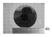
図7は、本発明に従い形成された炭化ケイ素ウェーハの3つの写真の組である。図7(A)および図7(B)は、わずかに垂直でない角度で撮られ、従ってウェーハは、写真の中で長円形に見える。しかしながら、図7(C)の正面写真によって例示されるように、ウェーハは円形である。これらの写真は、本発明に従い産生された100mmのウェーハを示す。 FIG. 7 is a set of three photographs of a silicon carbide wafer formed in accordance with the present invention. FIGS. 7A and 7B are taken at a slightly non-vertical angle, so the wafer appears oval in the photograph. However, the wafer is circular as illustrated by the front photo in FIG. These photographs show a 100 mm wafer produced according to the present invention.
図8は、該方法およびその利点の局面を例示する概略図である。図8は、向かい合う面71および72が、c面73に関して軸オフである、70で広く示されたバルク結晶を例示する。参照の目的のために、c軸74もまた示される。明瞭にするために、図8は、軸オフの配向の程度を誇張している。
FIG. 8 is a schematic diagram illustrating aspects of the method and its advantages. FIG. 8 illustrates a bulk crystal broadly shown at 70, where the opposing faces 71 and 72 are off-axis with respect to the c-
該方法に従うと、成長した結晶の面71、72は、結晶のc面に関してすでに軸オフであることから、結晶70が、均質の直立した円柱という形で(一般的であるように)成長すると仮定すれば、結晶70は、軸オフの表面を有する個々のウェーハ75を規定するために、その円筒の軸と直角に切断され得、長円形ではなく円形において切断され得る。
According to the method, the grown crystal faces 71, 72 are already off-axis with respect to the c-plane of the crystal, so that the
本明細書中に記載された技術は、SiCの(0001)面および[0001]軸に関して記載されたけれども、該技術が、他の面(例えば、{0001}平面)を用いて、他の軸に関して、組込まれ得ることが理解されるであろう。多くの理由のために、(0001)面および Although the techniques described herein have been described with respect to the (0001) plane and the [0001] axis of SiC, the technique uses other planes (eg, the {0001} plane) to It will be appreciated that can be incorporated with respect to. For many reasons, the (0001) plane and
![]()
![]()
用語「単結晶」が、なんらかのモザイク模様の性質を有する大型のブール結晶を記述するために用いられ得ることはまた、炭化ケイ素の結晶の成長に詳しい人々によって理解される。当業者にさらに公知であるように、モザイク模様の性質を有する結晶は、単結晶を形成するために、共に成長する複数の核になる領域とともに成長する。結果としてもたらされる領域は、転位または他の欠陥に接し得るけれども、それにもかかわらず、よく理解されている技術(特に、X線回折)によって分析されるときに、単結晶の特性を有する。これらの領域の集合体は、粒(grain)間で非常に小傾角の領域(small tilt region)によってモザイク構造を有し得るけれども、領域は、なお共に成長して単結晶を形成する。 It is also understood by those familiar with the growth of silicon carbide crystals that the term “single crystal” can be used to describe a large boule crystal having some mosaic nature. As is further known to those skilled in the art, crystals having a mosaic pattern grow with multiple core regions that grow together to form a single crystal. Although the resulting region may be in contact with dislocations or other defects, it nevertheless has the properties of a single crystal when analyzed by well-understood techniques (especially X-ray diffraction). Although the collection of these regions can have a mosaic structure with very small tilt regions between the grains, the regions still grow together to form a single crystal.
X線回折によって、本発明に従って成長した結晶の単結晶の特性は、角度の約36秒と180秒との間の回折角からの角度の幅を有する。これは、40秒〜60秒(sec−1)の角度の幅が高品質な単結晶を表す、当該分野における単結晶の許容範囲の標準的範囲を満足する。角度の幅は、当該分野においてよく理解されている標準と一致する、ブラッグ角におけるスペクトル半値幅(FWHM)として測定される。 By X-ray diffraction, the single crystal properties of a crystal grown according to the present invention have an angular width from a diffraction angle between about 36 and 180 seconds of angle. This satisfies the standard range of single crystal tolerances in the art, which represents a high quality single crystal with an angular width of 40 seconds to 60 seconds (sec −1 ). The width of the angle is measured as the spectral half width (FWHM) at the Bragg angle, consistent with a standard well understood in the art.
図面および明細書において、本発明の好適な実施形態が示され、特定の用語が利用されたけれども、それらは、単に一般的な、説明的な意味において用いられ、特許請求の範囲に規定される本発明の範囲を制限する目的のためではない。 Although preferred embodiments of the invention are shown in the drawings and specification and specific terms have been utilized, they are merely used in a general, descriptive sense and are defined in the claims. It is not for the purpose of limiting the scope of the invention.
Claims (29)
種結晶部分と、
該種結晶部分上の成長部分と、
実質的に直立した円筒形の炭化ケイ素の単結晶を形成する該種結晶部分および該成長部分と、
該成長部分と該種結晶部分との間の界面を規定する種結晶面であって、該種結晶面は、該直立した円筒形の結晶の基部に実質的に平行であり、該単結晶の基底平面に関して軸オフである、種結晶面と、
該種結晶部分のポリタイプを複製する該成長部分と、
少なくとも約100mmの直径を有する該成長部分と
を含む、半導体結晶。 A semiconductor crystal,
A seed crystal portion;
A growing portion on the seed crystal portion;
The seed crystal portion and the growth portion forming a substantially upright cylindrical silicon carbide single crystal;
A seed crystal plane defining an interface between the growing portion and the seed crystal portion, the seed crystal plane being substantially parallel to a base of the upright cylindrical crystal, A seed plane that is off-axis with respect to the ground plane; and
The growing portion replicating the polytype of the seed crystal portion;
And a growing portion having a diameter of at least about 100 mm.
単結晶の種結晶部分と、
該種結晶部分上の単結晶の成長部分と、
少なくとも直径100ミリメートルの直立した円筒形の炭化ケイ素の単結晶を規定するために十分な直径を有する該種結晶部分および該成長部分と、
該成長部分と該種結晶部分との間の界面を規定する種結晶面であって、該種結晶面は、該直立した円筒形の結晶の基部に実質的に平行であり、該単結晶の{0001}平面に関して約0.5°と12°との間の軸オフである、種結晶面と、
該種結晶部分のポリタイプを複製する該成長部分と
を含む、半導体ウェーハ。 A semiconductor wafer,
A seed crystal portion of a single crystal;
A single crystal growth portion on the seed crystal portion;
The seed crystal portion and the growth portion having a diameter sufficient to define an upright cylindrical silicon carbide single crystal of at least 100 millimeters in diameter;
A seed crystal plane defining an interface between the growing portion and the seed crystal portion, the seed crystal plane being substantially parallel to a base of the upright cylindrical crystal, A seed plane that is off axis between about 0.5 ° and 12 ° with respect to the {0001} plane;
And a growth portion replicating the polytype of the seed crystal portion.
炭化ケイ素のバルク単結晶から該バルク結晶のc軸に関してある角度で炭化ケイ素の種結晶を切断することであって、該バルク結晶は、該バルク結晶のc面に関して軸オフである面を有する種結晶を産生する、切断することと、
シードされた成長システムにおける該軸オフの種結晶に対して顕著な温度勾配を適用することにより、該種結晶の軸方向の配向を複製する、結果もたらされるバルク結晶を産生することと、
該種結晶の原初の面に平行に該バルク結晶を切断することによって該バルク結晶からウェーハを切断して、該種結晶ウェーハの{0001}平面に関して軸オフである面を有するウェーハを産生することと
を包含する、方法。 A method for growing a high quality, large diameter, silicon carbide single crystal comprising:
Cutting a silicon carbide seed crystal from a silicon carbide bulk single crystal at an angle with respect to the c-axis of the bulk crystal, wherein the bulk crystal is a seed having a plane that is off-axis with respect to the c-plane of the bulk crystal. Producing crystals, cutting,
Applying a significant temperature gradient to the off-axis seed crystal in a seeded growth system to produce a resulting bulk crystal that replicates the axial orientation of the seed crystal;
Cutting a wafer from the bulk crystal by cutting the bulk crystal parallel to the original surface of the seed crystal to produce a wafer having a surface that is off-axis with respect to the {0001} plane of the seed crystal wafer. And a method comprising.
Applications Claiming Priority (2)
| Application Number | Priority Date | Filing Date | Title |
|---|---|---|---|
| US11/428,954 US8980445B2 (en) | 2006-07-06 | 2006-07-06 | One hundred millimeter SiC crystal grown on off-axis seed |
| PCT/US2007/069946 WO2008005636A1 (en) | 2006-07-06 | 2007-05-30 | One hundred millimeter sic crystal grown on off-axis seed |
Related Child Applications (1)
| Application Number | Title | Priority Date | Filing Date |
|---|---|---|---|
| JP2012228190A Division JP2013018706A (en) | 2006-07-06 | 2012-10-15 | ONE HUNDRED MILLIMETER SiC CRYSTAL GROWN ON OFF-AXIS SEED CRYSTAL |
Publications (1)
| Publication Number | Publication Date |
|---|---|
| JP2009542571A true JP2009542571A (en) | 2009-12-03 |
Family
ID=38616288
Family Applications (2)
| Application Number | Title | Priority Date | Filing Date |
|---|---|---|---|
| JP2009518424A Pending JP2009542571A (en) | 2006-07-06 | 2007-05-30 | Growth of 100 mm silicon carbide crystals on off-axis seed crystals |
| JP2012228190A Pending JP2013018706A (en) | 2006-07-06 | 2012-10-15 | ONE HUNDRED MILLIMETER SiC CRYSTAL GROWN ON OFF-AXIS SEED CRYSTAL |
Family Applications After (1)
| Application Number | Title | Priority Date | Filing Date |
|---|---|---|---|
| JP2012228190A Pending JP2013018706A (en) | 2006-07-06 | 2012-10-15 | ONE HUNDRED MILLIMETER SiC CRYSTAL GROWN ON OFF-AXIS SEED CRYSTAL |
Country Status (6)
| Country | Link |
|---|---|
| US (1) | US8980445B2 (en) |
| EP (1) | EP2038455B1 (en) |
| JP (2) | JP2009542571A (en) |
| CN (1) | CN101484616B (en) |
| RU (1) | RU2418891C9 (en) |
| WO (1) | WO2008005636A1 (en) |
Cited By (2)
| Publication number | Priority date | Publication date | Assignee | Title |
|---|---|---|---|---|
| JP2013018706A (en) * | 2006-07-06 | 2013-01-31 | Cree Inc | ONE HUNDRED MILLIMETER SiC CRYSTAL GROWN ON OFF-AXIS SEED CRYSTAL |
| JP2017190286A (en) * | 2017-07-20 | 2017-10-19 | 住友電気工業株式会社 | Silicon carbide single crystal substrate |
Families Citing this family (39)
| Publication number | Priority date | Publication date | Assignee | Title |
|---|---|---|---|---|
| JP2010076967A (en) * | 2008-09-25 | 2010-04-08 | Sumitomo Electric Ind Ltd | Production method of silicon carbide substrate, and silicon carbide substrate |
| JP5480169B2 (en) | 2011-01-13 | 2014-04-23 | 浜松ホトニクス株式会社 | Laser processing method |
| CN103608498B (en) | 2011-07-20 | 2018-04-10 | 住友电气工业株式会社 | Silicon carbide substrates, semiconductor device and their manufacture method |
| JP5803786B2 (en) * | 2012-04-02 | 2015-11-04 | 住友電気工業株式会社 | Silicon carbide substrate, semiconductor device and manufacturing method thereof |
| US8860040B2 (en) | 2012-09-11 | 2014-10-14 | Dow Corning Corporation | High voltage power semiconductor devices on SiC |
| US9018639B2 (en) | 2012-10-26 | 2015-04-28 | Dow Corning Corporation | Flat SiC semiconductor substrate |
| US9017804B2 (en) | 2013-02-05 | 2015-04-28 | Dow Corning Corporation | Method to reduce dislocations in SiC crystal growth |
| US9797064B2 (en) * | 2013-02-05 | 2017-10-24 | Dow Corning Corporation | Method for growing a SiC crystal by vapor deposition onto a seed crystal provided on a support shelf which permits thermal expansion |
| US9738991B2 (en) * | 2013-02-05 | 2017-08-22 | Dow Corning Corporation | Method for growing a SiC crystal by vapor deposition onto a seed crystal provided on a supporting shelf which permits thermal expansion |
| US8940614B2 (en) | 2013-03-15 | 2015-01-27 | Dow Corning Corporation | SiC substrate with SiC epitaxial film |
| US9657409B2 (en) | 2013-05-02 | 2017-05-23 | Melior Innovations, Inc. | High purity SiOC and SiC, methods compositions and applications |
| US10322936B2 (en) | 2013-05-02 | 2019-06-18 | Pallidus, Inc. | High purity polysilocarb materials, applications and processes |
| US9919972B2 (en) | 2013-05-02 | 2018-03-20 | Melior Innovations, Inc. | Pressed and self sintered polymer derived SiC materials, applications and devices |
| US11091370B2 (en) | 2013-05-02 | 2021-08-17 | Pallidus, Inc. | Polysilocarb based silicon carbide materials, applications and devices |
| JP6183010B2 (en) * | 2013-07-03 | 2017-08-23 | 住友電気工業株式会社 | Silicon carbide single crystal substrate and method for manufacturing the same |
| US9279192B2 (en) | 2014-07-29 | 2016-03-08 | Dow Corning Corporation | Method for manufacturing SiC wafer fit for integration with power device manufacturing technology |
| JP6395632B2 (en) | 2015-02-09 | 2018-09-26 | 株式会社ディスコ | Wafer generation method |
| JP6395633B2 (en) | 2015-02-09 | 2018-09-26 | 株式会社ディスコ | Wafer generation method |
| JP6429715B2 (en) | 2015-04-06 | 2018-11-28 | 株式会社ディスコ | Wafer generation method |
| JP6425606B2 (en) | 2015-04-06 | 2018-11-21 | 株式会社ディスコ | Wafer production method |
| JP6494382B2 (en) | 2015-04-06 | 2019-04-03 | 株式会社ディスコ | Wafer generation method |
| JP6472333B2 (en) | 2015-06-02 | 2019-02-20 | 株式会社ディスコ | Wafer generation method |
| JP6482423B2 (en) | 2015-07-16 | 2019-03-13 | 株式会社ディスコ | Wafer generation method |
| JP6482425B2 (en) | 2015-07-21 | 2019-03-13 | 株式会社ディスコ | Thinning method of wafer |
| JP6472347B2 (en) | 2015-07-21 | 2019-02-20 | 株式会社ディスコ | Thinning method of wafer |
| JP6690983B2 (en) | 2016-04-11 | 2020-04-28 | 株式会社ディスコ | Wafer generation method and actual second orientation flat detection method |
| CN106435732B (en) * | 2016-08-30 | 2019-08-30 | 河北同光晶体有限公司 | A kind of method of quick preparation large scale SiC single crystal crystal bar |
| JP6858587B2 (en) | 2017-02-16 | 2021-04-14 | 株式会社ディスコ | Wafer generation method |
| JP7035377B2 (en) * | 2017-03-27 | 2022-03-15 | ウシオ電機株式会社 | Semiconductor laser device |
| US11114817B2 (en) * | 2017-03-27 | 2021-09-07 | Ushio Denki Kabushiki Kaisha | Semiconductor laser device |
| US10679898B2 (en) * | 2018-04-27 | 2020-06-09 | Semiconductor Components Industries, Llc | Semiconductor substrate die sawing singulation systems and methods |
| US10562130B1 (en) | 2018-12-29 | 2020-02-18 | Cree, Inc. | Laser-assisted method for parting crystalline material |
| US11024501B2 (en) | 2018-12-29 | 2021-06-01 | Cree, Inc. | Carrier-assisted method for parting crystalline material along laser damage region |
| US10576585B1 (en) | 2018-12-29 | 2020-03-03 | Cree, Inc. | Laser-assisted method for parting crystalline material |
| US10611052B1 (en) | 2019-05-17 | 2020-04-07 | Cree, Inc. | Silicon carbide wafers with relaxed positive bow and related methods |
| CN115279956A (en) | 2019-12-27 | 2022-11-01 | 沃孚半导体公司 | Large diameter silicon carbide wafer |
| CN113122914B (en) * | 2020-06-09 | 2023-02-28 | 北京世纪金光半导体有限公司 | Device for maintaining stability of large-size silicon carbide crystal form and growth method |
| US12024794B2 (en) | 2021-06-17 | 2024-07-02 | Wolfspeed, Inc. | Reduced optical absorption for silicon carbide crystalline materials |
| CN114347277B (en) * | 2021-11-30 | 2024-04-19 | 中国电子科技集团公司第十一研究所 | InSb wafer preparation method |
Citations (9)
| Publication number | Priority date | Publication date | Assignee | Title |
|---|---|---|---|---|
| JPH0416597A (en) * | 1990-05-09 | 1992-01-21 | Sharp Corp | Production of silicon carbide single crystal |
| JPH08245299A (en) * | 1995-03-10 | 1996-09-24 | Sanyo Electric Co Ltd | Method for growing silicon carbide crystal |
| JPH1022526A (en) * | 1995-05-19 | 1998-01-23 | Sanyo Electric Co Ltd | Semiconductor light emitting element, semiconductor laser element and manufacturing of the semiconductor light emitting element |
| JP2000340512A (en) * | 1999-03-23 | 2000-12-08 | Matsushita Electric Ind Co Ltd | Method for growing semiconductor film and manufacture for semiconductor device |
| JP2004099340A (en) * | 2002-09-05 | 2004-04-02 | Nippon Steel Corp | Seed crystal for silicon carbide single crystal growth, silicon carbide single crystal ingot and method of manufacturing the same |
| JP2005179155A (en) * | 2003-12-22 | 2005-07-07 | Toyota Central Res & Dev Lab Inc | METHOD FOR PRODUCING SiC SINGLE CRYSTAL |
| WO2006041660A2 (en) * | 2004-10-04 | 2006-04-20 | Cree, Inc. | 100 mm silicon carbide wafer with low micropipe density |
| JP2006111478A (en) * | 2004-10-13 | 2006-04-27 | Nippon Steel Corp | Silicon carbide single crystal ingot, silicon carbide single crystal wafer, and its manufacturing method |
| JP2006117512A (en) * | 2004-09-24 | 2006-05-11 | Showa Denko Kk | Method for producing silicon carbide single crystal and silicon carbide single crystal grown by the method, single crystal ingot and silicon carbide single crystal wafer |
Family Cites Families (23)
| Publication number | Priority date | Publication date | Assignee | Title |
|---|---|---|---|---|
| US4912064A (en) * | 1987-10-26 | 1990-03-27 | North Carolina State University | Homoepitaxial growth of alpha-SiC thin films and semiconductor devices fabricated thereon |
| US4866005A (en) * | 1987-10-26 | 1989-09-12 | North Carolina State University | Sublimation of silicon carbide to produce large, device quality single crystals of silicon carbide |
| US4918497A (en) * | 1988-12-14 | 1990-04-17 | Cree Research, Inc. | Blue light emitting diode formed in silicon carbide |
| US5958132A (en) | 1991-04-18 | 1999-09-28 | Nippon Steel Corporation | SiC single crystal and method for growth thereof |
| US5248385A (en) * | 1991-06-12 | 1993-09-28 | The United States Of America, As Represented By The Administrator, National Aeronautics And Space Administration | Process for the homoepitaxial growth of single-crystal silicon carbide films on silicon carbide wafers |
| US5592501A (en) * | 1994-09-20 | 1997-01-07 | Cree Research, Inc. | Low-strain laser structures with group III nitride active layers |
| DE19527536A1 (en) * | 1995-07-27 | 1997-01-30 | Siemens Ag | Process for the production of silicon carbide single crystals |
| US5769941A (en) * | 1996-05-01 | 1998-06-23 | Motorola, Inc. | Method of forming semiconductor material |
| US6316793B1 (en) * | 1998-06-12 | 2001-11-13 | Cree, Inc. | Nitride based transistors on semi-insulating silicon carbide substrates |
| DE50002072D1 (en) * | 1999-02-19 | 2003-06-12 | Siemens Ag | METHOD FOR GROWING A DOLLAR G (A) -SIC VOLUME SINGLE CRYSTAL |
| EP1200651B1 (en) * | 1999-07-07 | 2004-04-07 | Siemens Aktiengesellschaft | Seed crystal holder with a lateral border for an sic seed crystal |
| JP4304783B2 (en) | 1999-09-06 | 2009-07-29 | 住友電気工業株式会社 | SiC single crystal and growth method thereof |
| SE520968C2 (en) * | 2001-10-29 | 2003-09-16 | Okmetic Oyj | High-resistance monocrystalline silicon carbide and its method of preparation |
| US7601441B2 (en) * | 2002-06-24 | 2009-10-13 | Cree, Inc. | One hundred millimeter high purity semi-insulating single crystal silicon carbide wafer |
| FR2852974A1 (en) * | 2003-03-31 | 2004-10-01 | Soitec Silicon On Insulator | PROCESS FOR THE PRODUCTION OF MONOCRYSTALLINE CRYSTALS |
| JP3764462B2 (en) * | 2003-04-10 | 2006-04-05 | 株式会社豊田中央研究所 | Method for producing silicon carbide single crystal |
| JP4407188B2 (en) * | 2003-07-23 | 2010-02-03 | 信越半導体株式会社 | Silicon wafer manufacturing method and silicon wafer |
| JP3888374B2 (en) * | 2004-03-17 | 2007-02-28 | 住友電気工業株式会社 | Manufacturing method of GaN single crystal substrate |
| JP4694144B2 (en) | 2004-05-14 | 2011-06-08 | 住友電気工業株式会社 | Method for growing SiC single crystal and SiC single crystal grown thereby |
| EP1619276B1 (en) * | 2004-07-19 | 2017-01-11 | Norstel AB | Homoepitaxial growth of SiC on low off-axis SiC wafers |
| US7192482B2 (en) * | 2004-08-10 | 2007-03-20 | Cree, Inc. | Seed and seedholder combinations for high quality growth of large silicon carbide single crystals |
| US7314520B2 (en) * | 2004-10-04 | 2008-01-01 | Cree, Inc. | Low 1c screw dislocation 3 inch silicon carbide wafer |
| US8980445B2 (en) | 2006-07-06 | 2015-03-17 | Cree, Inc. | One hundred millimeter SiC crystal grown on off-axis seed |
-
2006
- 2006-07-06 US US11/428,954 patent/US8980445B2/en active Active
-
2007
- 2007-05-30 JP JP2009518424A patent/JP2009542571A/en active Pending
- 2007-05-30 EP EP07797873.2A patent/EP2038455B1/en active Active
- 2007-05-30 WO PCT/US2007/069946 patent/WO2008005636A1/en active Application Filing
- 2007-05-30 RU RU2008152451/05A patent/RU2418891C9/en active
- 2007-05-30 CN CN200780025613.9A patent/CN101484616B/en active Active
-
2012
- 2012-10-15 JP JP2012228190A patent/JP2013018706A/en active Pending
Patent Citations (9)
| Publication number | Priority date | Publication date | Assignee | Title |
|---|---|---|---|---|
| JPH0416597A (en) * | 1990-05-09 | 1992-01-21 | Sharp Corp | Production of silicon carbide single crystal |
| JPH08245299A (en) * | 1995-03-10 | 1996-09-24 | Sanyo Electric Co Ltd | Method for growing silicon carbide crystal |
| JPH1022526A (en) * | 1995-05-19 | 1998-01-23 | Sanyo Electric Co Ltd | Semiconductor light emitting element, semiconductor laser element and manufacturing of the semiconductor light emitting element |
| JP2000340512A (en) * | 1999-03-23 | 2000-12-08 | Matsushita Electric Ind Co Ltd | Method for growing semiconductor film and manufacture for semiconductor device |
| JP2004099340A (en) * | 2002-09-05 | 2004-04-02 | Nippon Steel Corp | Seed crystal for silicon carbide single crystal growth, silicon carbide single crystal ingot and method of manufacturing the same |
| JP2005179155A (en) * | 2003-12-22 | 2005-07-07 | Toyota Central Res & Dev Lab Inc | METHOD FOR PRODUCING SiC SINGLE CRYSTAL |
| JP2006117512A (en) * | 2004-09-24 | 2006-05-11 | Showa Denko Kk | Method for producing silicon carbide single crystal and silicon carbide single crystal grown by the method, single crystal ingot and silicon carbide single crystal wafer |
| WO2006041660A2 (en) * | 2004-10-04 | 2006-04-20 | Cree, Inc. | 100 mm silicon carbide wafer with low micropipe density |
| JP2006111478A (en) * | 2004-10-13 | 2006-04-27 | Nippon Steel Corp | Silicon carbide single crystal ingot, silicon carbide single crystal wafer, and its manufacturing method |
Cited By (3)
| Publication number | Priority date | Publication date | Assignee | Title |
|---|---|---|---|---|
| JP2013018706A (en) * | 2006-07-06 | 2013-01-31 | Cree Inc | ONE HUNDRED MILLIMETER SiC CRYSTAL GROWN ON OFF-AXIS SEED CRYSTAL |
| US8980445B2 (en) | 2006-07-06 | 2015-03-17 | Cree, Inc. | One hundred millimeter SiC crystal grown on off-axis seed |
| JP2017190286A (en) * | 2017-07-20 | 2017-10-19 | 住友電気工業株式会社 | Silicon carbide single crystal substrate |
Also Published As
| Publication number | Publication date |
|---|---|
| EP2038455B1 (en) | 2015-12-02 |
| RU2418891C2 (en) | 2011-05-20 |
| WO2008005636A1 (en) | 2008-01-10 |
| US8980445B2 (en) | 2015-03-17 |
| CN101484616A (en) | 2009-07-15 |
| US20080008641A1 (en) | 2008-01-10 |
| JP2013018706A (en) | 2013-01-31 |
| EP2038455A1 (en) | 2009-03-25 |
| RU2008152451A (en) | 2010-08-20 |
| RU2418891C9 (en) | 2011-09-10 |
| CN101484616B (en) | 2013-07-24 |
Similar Documents
| Publication | Publication Date | Title |
|---|---|---|
| JP2013018706A (en) | ONE HUNDRED MILLIMETER SiC CRYSTAL GROWN ON OFF-AXIS SEED CRYSTAL | |
| US9816202B2 (en) | Single crystal diamond | |
| JP5788433B2 (en) | Process for large-scale ammonothermal production of semipolar gallium nitride boule | |
| JP5496007B2 (en) | Finely graded gallium nitride substrate for high quality homoepitaxy | |
| JP4603386B2 (en) | Method for producing silicon carbide single crystal | |
| TW201002879A (en) | Methods for producing improved crystallinity group III-nitride crystals from initial group III-nitride seed by ammonothermal growth | |
| US10156530B2 (en) | Group III nitride wafers and fabrication method and testing method | |
| Si et al. | Investigations of 3C-SiC inclusions in 4H-SiC epilayers on 4H-SiC single crystal substrates | |
| US6461944B2 (en) | Methods for growth of relatively large step-free SiC crystal surfaces | |
| JP6120742B2 (en) | Method for manufacturing single crystal ingot, method for manufacturing single crystal substrate, and method for manufacturing semiconductor device | |
| JP2010042980A (en) | Method for producing group iii nitride crystal and group iii nitride crystal | |
| JP2020002003A (en) | Chamfered silicon carbide substrate and chamfering method | |
| JP6526811B2 (en) | Method of processing a group III nitride crystal | |
| WO2021154484A1 (en) | Dislocation distribution for silicon carbide crystalline materials | |
| Zhang et al. | Morphology and crystalline property of an AlN single crystal grown on AlN seed | |
| Powell et al. | Growth of SiC substrates | |
| JPH0797299A (en) | Method for growing sic single crystal | |
| Ohtani | Dislocation Formation During Physical Vapor Transport Growth of 4 H‐SiC Crystals | |
| Wu et al. | Characterization of dislocations and micropipes in 4H n+ SiC substrates | |
| Zhang et al. | The Effect of 4H-SiC Substrate Surface Scratches on Chemical Vapor Deposition Grown Homo-Epitaxial Layer Quality | |
| Tavernier et al. | Progress Toward Making Gallium Nitride Seed Crystals Using Hydride Vapor‐Phase Epitaxy | |
| Bakin | SiC homoepitaxy and heteroepitaxy | |
| POWELL et al. | Growth of SiC substrates |
Legal Events
| Date | Code | Title | Description |
|---|---|---|---|
| RD04 | Notification of resignation of power of attorney |
Free format text: JAPANESE INTERMEDIATE CODE: A7424 Effective date: 20110124 |
|
| RD02 | Notification of acceptance of power of attorney |
Free format text: JAPANESE INTERMEDIATE CODE: A7422 Effective date: 20110112 |
|
| A977 | Report on retrieval |
Free format text: JAPANESE INTERMEDIATE CODE: A971007 Effective date: 20111110 |
|
| A131 | Notification of reasons for refusal |
Free format text: JAPANESE INTERMEDIATE CODE: A131 Effective date: 20111118 |
|
| A601 | Written request for extension of time |
Free format text: JAPANESE INTERMEDIATE CODE: A601 Effective date: 20120220 |
|
| A602 | Written permission of extension of time |
Free format text: JAPANESE INTERMEDIATE CODE: A602 Effective date: 20120227 |
|
| A521 | Request for written amendment filed |
Free format text: JAPANESE INTERMEDIATE CODE: A523 Effective date: 20120319 |
|
| A02 | Decision of refusal |
Free format text: JAPANESE INTERMEDIATE CODE: A02 Effective date: 20120615 |
|
| A521 | Request for written amendment filed |
Free format text: JAPANESE INTERMEDIATE CODE: A523 Effective date: 20121015 |
|
| A911 | Transfer to examiner for re-examination before appeal (zenchi) |
Free format text: JAPANESE INTERMEDIATE CODE: A911 Effective date: 20121022 |
|
| A912 | Re-examination (zenchi) completed and case transferred to appeal board |
Free format text: JAPANESE INTERMEDIATE CODE: A912 Effective date: 20121109 |