JP2009509357A - Magnetic element having stabilized ferromagnetic free layer or ferromagnetic free layer laminated structure - Google Patents
Magnetic element having stabilized ferromagnetic free layer or ferromagnetic free layer laminated structure Download PDFInfo
- Publication number
- JP2009509357A JP2009509357A JP2008532331A JP2008532331A JP2009509357A JP 2009509357 A JP2009509357 A JP 2009509357A JP 2008532331 A JP2008532331 A JP 2008532331A JP 2008532331 A JP2008532331 A JP 2008532331A JP 2009509357 A JP2009509357 A JP 2009509357A
- Authority
- JP
- Japan
- Prior art keywords
- layer
- ferromagnetic
- free layer
- ferromagnetic free
- magnetic bias
- Prior art date
- Legal status (The legal status is an assumption and is not a legal conclusion. Google has not performed a legal analysis and makes no representation as to the accuracy of the status listed.)
- Pending
Links
Images


Classifications
-
- H—ELECTRICITY
- H10—SEMICONDUCTOR DEVICES; ELECTRIC SOLID-STATE DEVICES NOT OTHERWISE PROVIDED FOR
- H10N—ELECTRIC SOLID-STATE DEVICES NOT OTHERWISE PROVIDED FOR
- H10N50/00—Galvanomagnetic devices
- H10N50/10—Magnetoresistive devices
-
- B—PERFORMING OPERATIONS; TRANSPORTING
- B82—NANOTECHNOLOGY
- B82Y—SPECIFIC USES OR APPLICATIONS OF NANOSTRUCTURES; MEASUREMENT OR ANALYSIS OF NANOSTRUCTURES; MANUFACTURE OR TREATMENT OF NANOSTRUCTURES
- B82Y25/00—Nanomagnetism, e.g. magnetoimpedance, anisotropic magnetoresistance, giant magnetoresistance or tunneling magnetoresistance
-
- G—PHYSICS
- G11—INFORMATION STORAGE
- G11B—INFORMATION STORAGE BASED ON RELATIVE MOVEMENT BETWEEN RECORD CARRIER AND TRANSDUCER
- G11B5/00—Recording by magnetisation or demagnetisation of a record carrier; Reproducing by magnetic means; Record carriers therefor
- G11B5/127—Structure or manufacture of heads, e.g. inductive
- G11B5/33—Structure or manufacture of flux-sensitive heads, i.e. for reproduction only; Combination of such heads with means for recording or erasing only
- G11B5/39—Structure or manufacture of flux-sensitive heads, i.e. for reproduction only; Combination of such heads with means for recording or erasing only using magneto-resistive devices or effects
- G11B5/3903—Structure or manufacture of flux-sensitive heads, i.e. for reproduction only; Combination of such heads with means for recording or erasing only using magneto-resistive devices or effects using magnetic thin film layers or their effects, the films being part of integrated structures
- G11B5/398—Specially shaped layers
- G11B5/3983—Specially shaped layers with current confined paths in the spacer layer
-
- G—PHYSICS
- G11—INFORMATION STORAGE
- G11C—STATIC STORES
- G11C11/00—Digital stores characterised by the use of particular electric or magnetic storage elements; Storage elements therefor
- G11C11/02—Digital stores characterised by the use of particular electric or magnetic storage elements; Storage elements therefor using magnetic elements
- G11C11/16—Digital stores characterised by the use of particular electric or magnetic storage elements; Storage elements therefor using magnetic elements using elements in which the storage effect is based on magnetic spin effect
- G11C11/161—Digital stores characterised by the use of particular electric or magnetic storage elements; Storage elements therefor using magnetic elements using elements in which the storage effect is based on magnetic spin effect details concerning the memory cell structure, e.g. the layers of the ferromagnetic memory cell
-
- G—PHYSICS
- G11—INFORMATION STORAGE
- G11C—STATIC STORES
- G11C11/00—Digital stores characterised by the use of particular electric or magnetic storage elements; Storage elements therefor
- G11C11/02—Digital stores characterised by the use of particular electric or magnetic storage elements; Storage elements therefor using magnetic elements
- G11C11/16—Digital stores characterised by the use of particular electric or magnetic storage elements; Storage elements therefor using magnetic elements using elements in which the storage effect is based on magnetic spin effect
- G11C11/165—Auxiliary circuits
- G11C11/1659—Cell access
-
- H—ELECTRICITY
- H01—ELECTRIC ELEMENTS
- H01F—MAGNETS; INDUCTANCES; TRANSFORMERS; SELECTION OF MATERIALS FOR THEIR MAGNETIC PROPERTIES
- H01F10/00—Thin magnetic films, e.g. of one-domain structure
- H01F10/32—Spin-exchange-coupled multilayers, e.g. nanostructured superlattices
- H01F10/324—Exchange coupling of magnetic film pairs via a very thin non-magnetic spacer, e.g. by exchange with conduction electrons of the spacer
- H01F10/3254—Exchange coupling of magnetic film pairs via a very thin non-magnetic spacer, e.g. by exchange with conduction electrons of the spacer the spacer being semiconducting or insulating, e.g. for spin tunnel junction [STJ]
-
- H—ELECTRICITY
- H01—ELECTRIC ELEMENTS
- H01F—MAGNETS; INDUCTANCES; TRANSFORMERS; SELECTION OF MATERIALS FOR THEIR MAGNETIC PROPERTIES
- H01F10/00—Thin magnetic films, e.g. of one-domain structure
- H01F10/32—Spin-exchange-coupled multilayers, e.g. nanostructured superlattices
- H01F10/324—Exchange coupling of magnetic film pairs via a very thin non-magnetic spacer, e.g. by exchange with conduction electrons of the spacer
- H01F10/3268—Exchange coupling of magnetic film pairs via a very thin non-magnetic spacer, e.g. by exchange with conduction electrons of the spacer the exchange coupling being asymmetric, e.g. by use of additional pinning, by using antiferromagnetic or ferromagnetic coupling interface, i.e. so-called spin-valve [SV] structure, e.g. NiFe/Cu/NiFe/FeMn
-
- H—ELECTRICITY
- H10—SEMICONDUCTOR DEVICES; ELECTRIC SOLID-STATE DEVICES NOT OTHERWISE PROVIDED FOR
- H10B—ELECTRONIC MEMORY DEVICES
- H10B61/00—Magnetic memory devices, e.g. magnetoresistive RAM [MRAM] devices
- H10B61/20—Magnetic memory devices, e.g. magnetoresistive RAM [MRAM] devices comprising components having three or more electrodes, e.g. transistors
- H10B61/22—Magnetic memory devices, e.g. magnetoresistive RAM [MRAM] devices comprising components having three or more electrodes, e.g. transistors of the field-effect transistor [FET] type
-
- H—ELECTRICITY
- H10—SEMICONDUCTOR DEVICES; ELECTRIC SOLID-STATE DEVICES NOT OTHERWISE PROVIDED FOR
- H10N—ELECTRIC SOLID-STATE DEVICES NOT OTHERWISE PROVIDED FOR
- H10N50/00—Galvanomagnetic devices
- H10N50/80—Constructional details
- H10N50/85—Magnetic active materials
-
- H—ELECTRICITY
- H01—ELECTRIC ELEMENTS
- H01F—MAGNETS; INDUCTANCES; TRANSFORMERS; SELECTION OF MATERIALS FOR THEIR MAGNETIC PROPERTIES
- H01F10/00—Thin magnetic films, e.g. of one-domain structure
- H01F10/32—Spin-exchange-coupled multilayers, e.g. nanostructured superlattices
- H01F10/324—Exchange coupling of magnetic film pairs via a very thin non-magnetic spacer, e.g. by exchange with conduction electrons of the spacer
- H01F10/3254—Exchange coupling of magnetic film pairs via a very thin non-magnetic spacer, e.g. by exchange with conduction electrons of the spacer the spacer being semiconducting or insulating, e.g. for spin tunnel junction [STJ]
- H01F10/3259—Spin-exchange-coupled multilayers comprising at least a nanooxide layer [NOL], e.g. with a NOL spacer
-
- H—ELECTRICITY
- H01—ELECTRIC ELEMENTS
- H01F—MAGNETS; INDUCTANCES; TRANSFORMERS; SELECTION OF MATERIALS FOR THEIR MAGNETIC PROPERTIES
- H01F10/00—Thin magnetic films, e.g. of one-domain structure
- H01F10/32—Spin-exchange-coupled multilayers, e.g. nanostructured superlattices
- H01F10/324—Exchange coupling of magnetic film pairs via a very thin non-magnetic spacer, e.g. by exchange with conduction electrons of the spacer
- H01F10/3263—Exchange coupling of magnetic film pairs via a very thin non-magnetic spacer, e.g. by exchange with conduction electrons of the spacer the exchange coupling being symmetric, e.g. for dual spin valve, e.g. NiO/Co/Cu/Co/Cu/Co/NiO
Abstract
磁気トンネル接合または磁気抵抗トンネル接合(MJTs)、及びスピンバルブのような磁性多層構造は、強磁性自由層と隣接して形成され、かつ磁気結合して、例えば熱擾乱及び漏洩磁界によって生じる擾乱に対する所望の安定性を実現する磁性バイアス層を有する。低アスペクト比の安定なMTJセルは、例えば磁性バイアス層を使用する高密度MRAMメモリデバイス及び他のデバイスに対するCMOS処理を使用して形成することができる。このような多層構造に対する書き込みは、スピントランスファートルクによる書き込み電流を使用し、書き込み電流を層に直交する方向に流すことにより行なうことができる。各強磁性自由層は2つ以上の層を含むことができ、かつ強磁性自由層積層構造とすることができ、この積層構造は、第1及び第2強磁性層と、そして第1強磁性層と第2強磁性層との間の非磁性スペーサと、を含む。
【選択図】図1AMagnetic multilayer junctions such as magnetic tunnel junctions or magnetoresistive tunnel junctions (MJTs) and spin valves are formed adjacent to the ferromagnetic free layer and magnetically coupled to disturbances caused by, for example, thermal disturbances and leakage magnetic fields. It has a magnetic bias layer that achieves the desired stability. Low aspect ratio stable MTJ cells can be formed using high density MRAM memory devices using magnetic bias layers and CMOS processing for other devices, for example. Writing to such a multilayer structure can be performed by using a write current by spin transfer torque and flowing the write current in a direction perpendicular to the layer. Each ferromagnetic free layer can include two or more layers and can be a ferromagnetic free layer stack, which includes a first and second ferromagnetic layer, and a first ferromagnetic layer. A nonmagnetic spacer between the layer and the second ferromagnetic layer.
[Selection] Figure 1A
Description
本出願は、磁性材料、及び少なくとも一つの強磁性自由層を有する構造に関するものである。 The present application relates to a magnetic material and a structure having at least one ferromagnetic free layer.
本出願は次の米国特許出願の利益を主張する:
1.2005年9月20日出願の「安定化させた強磁性自由層を有する磁性素子」と題する同時係属中の米国特許出願第11/232,356号、及び
2.2006年8月1日出願の「強磁性自由層積層構造を有する磁性素子」と題する同時係属中の米国特許出願第11/498,294号。
This application claims the benefit of the following US patent applications:
1. Co-pending U.S. Patent Application No. 11 / 232,356, filed September 20, 2005, entitled "Magnetic Element with Stabilized Ferromagnetic Free Layer", and 2. August 1, 2006 Co-pending US patent application Ser. No. 11 / 498,294 entitled “Magnetic Element with Ferromagnetic Free Layer Laminate Structure”.
上記2つの米国出願の開示内容全体を参照することにより、開示内容全体が本出願の明細書の一部に組み込まれる。 By reference to the entire disclosure content of the above two US applications, the entire disclosure content is incorporated into the specification of the present application.
種々の磁性材料が多層構造に使用され、多層構造は「自由」層として構成される少なくとも一つの強磁性層を有し、「自由」層の磁化方向は外部磁界または制御電流によって変更することができる。磁気メモリデバイスは、このような多層構造を使用して構成することができ、多層構造では、情報は自由層の磁化方向に基づいて記憶される。 Various magnetic materials are used in the multilayer structure, which has at least one ferromagnetic layer configured as a “free” layer, and the magnetization direction of the “free” layer can be changed by an external magnetic field or a control current. it can. Magnetic memory devices can be constructed using such a multilayer structure, where information is stored based on the magnetization direction of the free layer.
このような多層構造の一例が磁気トンネル接合または磁気抵抗トンネル接合(magnetoresistive tunnel junction:MJT)であり、このトンネル接合は少なくとも3つの層:すなわち2つの強磁性層、及び2つの強磁性層の間のバリア層としての一つの非磁性絶縁体の薄膜層を含む。中間バリア層の絶縁体は導電性を示さないので、2つの強磁性層の間のバリアとして機能する。しかしながら、絶縁体の厚さが十分に薄い、例えば数ナノメートル以下である場合、2つの強磁性層の電子が絶縁体の薄膜層を、2つの強磁性層にバリア層を横切ってバイアス電圧が印加された状態で発生するトンネル効果に起因して「突き抜ける」ことができる。特に、MTJ構造を流れる電流に対する抵抗は、2つの強磁性層の磁化の相対的な向きによって変わる。2つの強磁性層の磁化が互いに平行である場合、MTJ構造における抵抗は最小値RPになる。2つの強磁性層の磁化が互いに反平行である場合、MTJ構造における抵抗は最大値RAPになる。この現象の大きさは普通、(RAP−RP)/RPとして定義されるトンネル磁気抵抗(tunneling magnetoresistance:TMR)によって特徴付けられる。 An example of such a multilayer structure is a magnetic tunnel junction or a magnetoresistive tunnel junction (MJT), which is at least three layers: between two ferromagnetic layers and two ferromagnetic layers. A non-magnetic insulator thin film layer as a barrier layer. Since the insulator of the intermediate barrier layer does not exhibit conductivity, it functions as a barrier between the two ferromagnetic layers. However, if the insulator thickness is sufficiently thin, eg, a few nanometers or less, the electrons in the two ferromagnetic layers cause the bias voltage across the insulator thin film layer and the two ferromagnetic layers across the barrier layer. It can “pierce” due to the tunnel effect that occurs in the applied state. In particular, the resistance to current flowing through the MTJ structure depends on the relative orientation of the magnetizations of the two ferromagnetic layers. When the magnetizations of the two ferromagnetic layers are parallel to each other, resistance in MTJ structure is minimal value R P. When the magnetizations of the two ferromagnetic layers are antiparallel to each other, the resistance in the MTJ structure has a maximum value RAP . The magnitude of this phenomenon is usually tunneling magnetoresistance, which is defined as (R AP -R P) / R P: characterized by (tunneling magnetoresistance TMR).
MJTを流れる電流に対する抵抗と、2つの強磁性層の間の相対磁化方向とのTMR効果における関係を不揮発性磁気メモリデバイスに使用して、情報をMTJ(磁気抵抗トンネル接合)の磁化状態により記憶することができる。TMR効果を利用する磁気ランダムアクセスメモリ(MRAM)デバイスは、例えば電子RAMデバイスに替わるデバイスとなる、または電子RAMデバイスに匹敵するデバイスとなることができる。このようなデバイスでは、一方の強磁性層が固定された磁化方向を有するように構成され、そして他方の強磁性層が「自由」層であり、この自由層の磁化方向は、固定された方向に対して平行になるように、または反対になるように変更することができる。情報は、MTJのバリアの2つの側での2つの強磁性層の相対的な磁化方向を利用して記憶される。例えば、バイナリービット「1」及び「0」は、MTJの2つの強磁性層の磁化が平行に配向する状態、及び反平行に配向する状態として記録することができる。MTJへのビット記録またはビット書き込みは、自由層の磁化方向を切り替えることにより、例えば電流を交差ストライプ状に配置される書き込みラインに供給することにより生成される書き込み磁界によって、スピントランスファー効果に基づいてMTJに電流を流すことによって、または他の手段によって行なうことができる。スピントランスファースイッチング(磁化反転)では、自由層の磁化の向きを変更するために必要な電流は非常に小さくすることができ(例えば、0.1mA以下)、かつ磁界の切り替えに使用される電流よりもずっと小さくすることができる。従って、MTJにおけるスピントランスファースイッチングを利用してセルの消費電力を大幅に減らすことができる。 The relationship between the resistance to the current flowing through the MJT and the relative magnetization direction between the two ferromagnetic layers in the TMR effect is used in a nonvolatile magnetic memory device, and information is stored by the magnetization state of the MTJ (magnetoresistance tunnel junction). can do. Magnetic random access memory (MRAM) devices that utilize the TMR effect can be, for example, devices that replace electronic RAM devices or devices that are comparable to electronic RAM devices. In such devices, one ferromagnetic layer is configured to have a fixed magnetization direction, and the other ferromagnetic layer is a “free” layer, and the magnetization direction of this free layer is a fixed direction. Can be changed to be parallel to or opposite. Information is stored utilizing the relative magnetization directions of the two ferromagnetic layers on the two sides of the MTJ barrier. For example, binary bits “1” and “0” can be recorded as the state in which the magnetizations of the two ferromagnetic layers of the MTJ are oriented in parallel and anti-parallel. Bit recording or bit writing to the MTJ is based on the spin transfer effect by switching the magnetization direction of the free layer, for example, by a write magnetic field generated by supplying a current to a write line arranged in a cross stripe shape. This can be done by passing a current through the MTJ or by other means. In spin transfer switching (magnetization reversal), the current required to change the magnetization direction of the free layer can be made very small (for example, 0.1 mA or less) and more than the current used for switching the magnetic field. Can be much smaller. Therefore, the power consumption of the cell can be greatly reduced by utilizing the spin transfer switching in the MTJ.
MTJセルを利用する磁気メモリデバイスの記憶容量を大きくしたいという要求により、各MTJセルを小さくして、所定のウェハ面積におけるMTJセルの個数を増やすことが必要になる。MTJセルのサイズが小さくなると、各セルにおけるMTJの磁化方向は、熱擾乱、磁気外乱、または超常磁性のような種々の要素の影響を受け易くなる。これは、一つの理由として、デジタルビットを記憶し、そして保持するMTJの保磁力に起因する磁気エネルギーがMTJセルのサイズとともに小さくなるからである。デジタルビットを記憶し、そして保持するための磁気エネルギーがセルサイズとともに小さくなって、普通、外乱発生源のエネルギーの複数倍である臨界値を下回ると、外乱エネルギーが、MTJセルの磁化状態を変化させ、従って記録ビットを変化させるために十分な大きさとなる恐れがある。従って、十分に小さいセルにおけるMTJの磁化方向は、これらの要素、及び他の要素のいずれかが発生する、または重なり合うことによって突発的に変更される恐れがあるので、MTJに記憶された情報が変化する、または消去される。外乱は、セルの周りの熱擾乱の熱エネルギー、またはMTJセルとセルからの漏洩磁界との間の相互作用に起因するエネルギーのような種々の要素によって発生する恐れがある。 In response to a request to increase the storage capacity of a magnetic memory device using MTJ cells, it is necessary to reduce each MTJ cell and increase the number of MTJ cells in a predetermined wafer area. As the size of the MTJ cell is reduced, the magnetization direction of the MTJ in each cell is more susceptible to various factors such as thermal disturbance, magnetic disturbance, or superparamagnetism. This is because, as one reason, the magnetic energy resulting from the coercivity of the MTJ that stores and holds digital bits decreases with the size of the MTJ cell. When the magnetic energy to store and hold the digital bits decreases with cell size, usually below a critical value that is multiple times the energy of the disturbance source, the disturbance energy changes the magnetization state of the MTJ cell And therefore may be large enough to change the recording bit. Therefore, since the magnetization direction of the MTJ in a sufficiently small cell may be changed suddenly due to the occurrence or overlap of these elements and other elements, the information stored in the MTJ Change or be erased. Disturbances can be generated by various factors, such as the thermal energy of the thermal disturbance around the cell, or the energy resulting from the interaction between the MTJ cell and the leakage magnetic field from the cell.
従って、MTJ及び他の多層構造における強磁性自由層の保磁力を大きくし、これによって強磁性自由層の磁化方向を種々の外乱に対して安定化させることが望ましい。 Therefore, it is desirable to increase the coercivity of the ferromagnetic free layer in the MTJ and other multilayer structures, thereby stabilizing the magnetization direction of the ferromagnetic free layer against various disturbances.
本出願は、種々の特徴の中でもとりわけ、磁性バイアス層を使用して自由層の保磁力を大きくし、熱擾乱及び漏洩磁界に対する磁気安定性を高める磁気トンネル接合または磁気抵抗トンネル接合(MJTs)、及び他の磁性多層構造について記述する。このようなMTJ及び他の磁性多層構造を使用して、磁気メモリセルを、各セルが低アスペクト比で小さく形成されるCMOS処理を利用する高密度MRAMチップのような高密度集積回路において形成することができる。 The present application provides, among other features, magnetic tunnel junctions or magnetoresistive tunnel junctions (MJTs) that use a magnetic bias layer to increase the coercivity of the free layer and increase magnetic stability against thermal disturbances and leakage magnetic fields, And other magnetic multilayer structures are described. Using such MTJs and other magnetic multilayer structures, magnetic memory cells are formed in a high density integrated circuit such as a high density MRAM chip utilizing CMOS processing where each cell is formed small with a low aspect ratio. be able to.
一の態様では、デバイスが、第1方向と、前記第1方向とほぼ反対の第2方向との間で変更することができる磁化方向を有する強磁性自由層を含むものとして記述される。磁性バイアス層もこのデバイスに、強磁性自由層と接触し、かつ磁気結合するように形成して、強磁性自由層の保磁力を大きくし、かつ強磁性自由層の磁化方向を、第1方向と、前記第1方向とほぼ反対の第2方向との間で変更することができるようにする。このデバイスは更に、ほぼ第1方向に沿って固定される磁化方向を有する強磁性固定層と、そして強磁性自由層積層構造と強磁性固定層との間に形成される絶縁バリア層と、を含み、絶縁バリア層によって、電子が、強磁性自由層と強磁性固定層との間に、かつ絶縁バリア層にバイアス電圧が印加された状態で強磁性自由層と強磁性固定層との間でトンネリングを起こすようになる。強磁性自由層は磁性バイアス層と絶縁バリア層との間に配置される。 In one aspect, a device is described as including a ferromagnetic free layer having a magnetization direction that can be varied between a first direction and a second direction substantially opposite the first direction. A magnetic bias layer is also formed on the device so as to be in contact with and magnetically coupled to the ferromagnetic free layer, to increase the coercive force of the ferromagnetic free layer and to change the magnetization direction of the ferromagnetic free layer in the first direction. And a second direction substantially opposite to the first direction. The device further includes a ferromagnetic pinned layer having a magnetization direction pinned substantially along a first direction, and an insulating barrier layer formed between the ferromagnetic free layer stack and the ferromagnetic pinned layer. The insulating barrier layer allows electrons to flow between the ferromagnetic free layer and the ferromagnetic pinned layer and between the ferromagnetic free layer and the ferromagnetic pinned layer with a bias voltage applied to the insulating barrier layer. Causes tunneling. The ferromagnetic free layer is disposed between the magnetic bias layer and the insulating barrier layer.
別の態様では、方法が以下の工程を含むものとして記述される。変更可能な磁化方向を有する強磁性自由層と、固定磁化方向を有する強磁性固定層と、そして強磁性自由層と強磁性固定層との間に形成される絶縁バリア層と、を含む磁気トンネル接合を設け、絶縁バリア層によって電子が、強磁性自由層と強磁性固定層との間に、かつ絶縁バリア層にバイアス電圧が印加された状態で強磁性自由層と強磁性固定層との間をトンネリングするようになる。更に、強磁性自由層と接触し、かつ磁気結合して強磁性自由層の磁化方向の変更を可能にしながら、強磁性自由層の保磁力を大きくする磁性バイアス層を設ける。強磁性自由層は磁性バイアス層と絶縁バリア層との間に配置される。 In another aspect, the method is described as comprising the following steps. A magnetic tunnel comprising a ferromagnetic free layer having a changeable magnetization direction, a ferromagnetic fixed layer having a fixed magnetization direction, and an insulating barrier layer formed between the ferromagnetic free layer and the ferromagnetic fixed layer A junction is provided, and electrons are transferred between the ferromagnetic free layer and the ferromagnetic pinned layer by the insulating barrier layer, and between the ferromagnetic free layer and the ferromagnetic pinned layer with a bias voltage applied to the insulating barrier layer. Will come to tunnel. Furthermore, a magnetic bias layer is provided that increases the coercivity of the ferromagnetic free layer while being in contact with the ferromagnetic free layer and magnetically coupled to allow the magnetization direction of the ferromagnetic free layer to be changed. The ferromagnetic free layer is disposed between the magnetic bias layer and the insulating barrier layer.
別の態様では、本出願はデバイスについて記述し、このデバイスは、変更可能な磁化方向を有する強磁性自由層と、そして強磁性自由層と接触し、かつ磁気結合するように形成されて強磁性自由層の保磁力を、強磁性自由層の磁化方向を固定することなく大きくする磁性バイアス層と、を含む。磁性バイアス層は、K・t<Jを満たす層厚t、異方性定数K、及び界面交換結合定数Jを有する。MTJは更に、所定方向に沿って固定される磁化方向を有する強磁性ピンド層と、そして強磁性ピンド層と接触し、かつ磁気結合して強磁性ピンド層の磁化方向を所定方向に沿って固定するように作用する反強磁性ピンニング層と、を含む。反強磁性ピンニング層はK’・t’>J’を満たす層厚t’、異方性定数K’、及び界面交換結合定数J’を有する。デバイスは更に、強磁性自由層と強磁性ピンド層との間に形成される中間層を含む。強磁性自由層は磁性バイアス層と中間層との間に配置される。一の実施形態では、中間層は、強磁性自由層と強磁性ピンド層との間に形成される絶縁バリア層とすることができ、絶縁バリア層によって電子が、絶縁バリア層にバイアス電圧が印加された状態で強磁性自由層と強磁性ピンド層との間でトンネリングを起こすようになる。別の実施形態では、中間層は非磁性金属層とすることができる。 In another aspect, the present application describes a device that is formed to contact and magnetically couple a ferromagnetic free layer having a changeable magnetization direction, and to be ferromagnetically coupled. And a magnetic bias layer that increases the coercivity of the free layer without fixing the magnetization direction of the ferromagnetic free layer. The magnetic bias layer has a layer thickness t that satisfies K · t <J, an anisotropy constant K, and an interface exchange coupling constant J. The MTJ further includes a ferromagnetic pinned layer having a magnetization direction fixed along a predetermined direction, and is in contact with the ferromagnetic pinned layer and magnetically coupled to fix the magnetization direction of the ferromagnetic pinned layer along the predetermined direction. An antiferromagnetic pinning layer that acts to The antiferromagnetic pinning layer has a layer thickness t ′ that satisfies K ′ · t ′> J ′, an anisotropy constant K ′, and an interface exchange coupling constant J ′. The device further includes an intermediate layer formed between the ferromagnetic free layer and the ferromagnetic pinned layer. The ferromagnetic free layer is disposed between the magnetic bias layer and the intermediate layer. In one embodiment, the intermediate layer can be an insulating barrier layer formed between the ferromagnetic free layer and the ferromagnetic pinned layer, where electrons are applied by the insulating barrier layer and a bias voltage is applied to the insulating barrier layer. In this state, tunneling occurs between the ferromagnetic free layer and the ferromagnetic pinned layer. In another embodiment, the intermediate layer can be a nonmagnetic metal layer.
更に別の態様では、本出願は、少なくとも強磁性自由層積層構造を有するMTJ構造について記述する。このような強磁性自由層積層構造の実施形態を使用して、単一の材料しか持たない自由層において実現することが難しい多数の利点をもたらすことができる。例えば、強磁性自由層積層構造内の非磁性バイアス層は拡散バリア層として機能して、堆積後アニール処理を行なっている間の不所望の拡散及び結晶配向形成を阻止することができる。 In yet another aspect, the present application describes an MTJ structure having at least a ferromagnetic free layer stack structure. Such ferromagnetic free layer stack embodiments can provide a number of advantages that are difficult to achieve in a free layer having only a single material. For example, the nonmagnetic bias layer in the ferromagnetic free layer stack can function as a diffusion barrier layer to prevent unwanted diffusion and crystal orientation formation during post-deposition annealing.
強磁性自由層積層構造を利用するデバイスに関する一つの例では、デバイスは基板と、そして基板上に形成される磁気セルと、を含む。磁気セルは強磁性自由層積層構造を含み、積層構造は第1方向と、前記第1方向とほぼ反対の第2方向との間で変更することができる正味の磁化の向きを有する。強磁性自由層積層構造は第1及び第2強磁性層と、そして第1強磁性層と第2強磁性層との間の非磁性スペーサと、を含む。強磁性固定層が固定磁化方向を有するように磁気セルに設けられる。磁気セルは更に、強磁性自由層積層構造と強磁性固定層との間に形成される絶縁バリア層を含み、絶縁バリア層によって、電子が、強磁性自由層積層構造と強磁性固定層との間に、かつ絶縁バリア層にバイアス電圧が印加された状態で強磁性自由層積層構造と強磁性固定層との間でトンネリングを起こすようになる。 In one example of a device that utilizes a ferromagnetic free layer stack, the device includes a substrate and a magnetic cell formed on the substrate. The magnetic cell includes a ferromagnetic free layer stack structure, the stack structure having a net magnetization orientation that can be changed between a first direction and a second direction substantially opposite the first direction. The ferromagnetic free layer stack structure includes first and second ferromagnetic layers and a nonmagnetic spacer between the first and second ferromagnetic layers. The ferromagnetic fixed layer is provided in the magnetic cell so as to have a fixed magnetization direction. The magnetic cell further includes an insulating barrier layer formed between the ferromagnetic free layer stack structure and the ferromagnetic pinned layer, and the insulating barrier layer allows electrons to be transferred between the ferromagnetic free layer stack structure and the ferromagnetic pinned layer. In the meantime, with the bias voltage applied to the insulating barrier layer, tunneling occurs between the ferromagnetic free layer stacked structure and the ferromagnetic pinned layer.
強磁性自由層積層構造を利用するデバイスに関する別の例では、上記デバイスは、強磁性自由層積層構造と接触し、かつ磁気結合して強磁性自由層積層構造の保磁力を大きくし、そして第1方向と、前記第1方向とほぼ反対の第2方向との間での強磁性自由層積層構造の磁化方向の変更を可能にする磁性バイアス層を含むことができる。 In another example of a device that utilizes a ferromagnetic free layer stack, the device is in contact with the ferromagnetic free layer stack and is magnetically coupled to increase the coercivity of the ferromagnetic free layer stack and A magnetic bias layer may be included that allows the magnetization direction of the ferromagnetic free layer stack structure to be changed between one direction and a second direction substantially opposite to the first direction.
これらの態様及び実施形態、及び他の態様及び実施形態、これらの態様及び実施形態の変更例及び変形例について更に詳細に、添付の図、詳細な記述、及び請求項において説明する。 These aspects and embodiments, as well as other aspects and embodiments, modifications and variations of these aspects and embodiments, are described in further detail in the accompanying drawings, detailed description, and claims.
磁性バイアス層を使用して本出願に記載される強磁性自由層を安定化させる方法は、種々の磁性多層構造に適用することができる。種々の実施形態では、強磁性自由層の磁化方向は、スピントランスファー効果を使用することにより切り替えることができる。MTJはこのような構造の単成る一例に過ぎない。強磁性自由層を有するこのような多層構造はスピンバルブ構造であり、スピンバルブ構造は、磁気メモリデバイス及び他の磁性素子に使用することもできる。スピンバルブは2つの強磁性層と、そして2つの強磁性層の間のスペーサ層としての一つの非磁性金属薄膜層と、を含むことができる。MTJと同様に、一方の強磁性層が固定層であり、そして他方の強磁性層が自由層である。スピンバルブの自由層は、MTJにおける自由層と同様の安定性の問題を示す。従って、バイアス層はスピンバルブにおいても用いることができる。以下の例ではMTJを、種々のバイアス層の構造、実施例、及び動作を示すための例として使用する。 The method of stabilizing a ferromagnetic free layer described in this application using a magnetic bias layer can be applied to various magnetic multilayer structures. In various embodiments, the magnetization direction of the ferromagnetic free layer can be switched by using the spin transfer effect. MTJ is just one example of such a structure. Such a multilayer structure with a ferromagnetic free layer is a spin valve structure, which can also be used for magnetic memory devices and other magnetic elements. The spin valve can include two ferromagnetic layers and one non-magnetic metal thin film layer as a spacer layer between the two ferromagnetic layers. Like the MTJ, one ferromagnetic layer is a fixed layer and the other ferromagnetic layer is a free layer. The free layer of the spin valve exhibits the same stability problem as the free layer in MTJ. Therefore, the bias layer can also be used in a spin valve. In the following examples, MTJ is used as an example to illustrate various bias layer structures, examples, and operations.
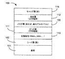
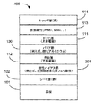
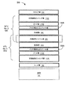
図1Aは、Si基板のような基板101の上に形成されるMTJ100の一つの例を示している。MTJ100は、基板101上に直接形成される一つ以上のシード層102の上に構成される。シード層102の上には、反強磁性(antiferromagnetic:AFM)層113がまず形成され、次に第1強磁性層111がAFM層113の上に形成される。ポストアニールを施した後、強磁性層111の磁化を後の時点でピン止めして、強磁性層111に固定磁化を付与する。或る実施形態では、この固定磁化の方向は基板101(すなわち、基板表面)に平行とすることができる。第1強磁性層111の上には、酸化金属層のような薄い絶縁バリア層130が設けられる。MTJ100では、第2強磁性層112がバリア層130の上に直接形成される。更に、少なくとも一つのキャップ層114が第2強磁性層112の上に形成されてMTJを保護する。
FIG. 1A shows an example of an
強磁性層112の磁化はピン止めされず、かつピンド層111の固定磁化方向と平行に、または反平行になるように、外部制御磁界、またはMTJに対して垂直方向に流れる駆動電流のいずれかを制御することによって自由に変化させることができる。このような理由により、層112は自由層(free layer:FL)である。磁界動作範囲の磁界によって、または接合に電流動作範囲の電流を流すことによって、自由層112の磁化の向きを強制的にピンド層111の固定磁化方向とほぼ平行に、またはほぼ反平行にすることができる。多くの磁場系では、静磁エネルギーが競合して、磁区またはナノ磁石が各強磁性層において完全な平行配向、または完全な反平行配向を示す現象を防止するように作用する。MTJでは、自由層112内のナノ磁石のエネルギー状態に大きな影響を与えることによって、ナノ磁石が強制的に平行配向または反平行配向を示すようになるので、ほぼ平行な配向またはほぼ反平行な配向が実現する。
The magnetization of the
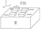
図1Bは、磁気メモリチップデバイスの一例を示しており、このチップデバイスでは、図1AのMTJ構造または他のMTJ構造を利用するMTJセルの2次元アレイがモノリシックに基板101の上に形成される。デカルト座標(x,y,z)を使用してチップの種々の寸法を示す。図1Bの矩形ブロックを使用してMTJセルの相対位置、及びメモリチップの各MTJセルの寸法を表わす。実際のデバイスでは、各セルは楕円形とすることができ、かつx方向に沿って長い。図1Cは、図1BのメモリチップのMTJを含む種々の構造の例示としての一つのレイアウトを示し、この場合、各MTJは基板上の金属ビアプラグの上に形成される。各MTJセルは、長さL1をx方向に沿って、そして長さL2をy方向に沿って有するものとして示され、この場合、x方向及びy方向はともに、基板の平面に平行である。各MTJのx方向及びy方向のアスペクト比はA=L1/L2と表わされる。メモリチップの単位面積当たりの記憶密度を大きくするために、L1及びL2の両方を小さくして、メモリデバイスにおける所定面積内のMTJセルの個数を増やす。
FIG. 1B shows an example of a magnetic memory chip device, in which a two-dimensional array of MTJ cells utilizing the MTJ structure of FIG. 1A or other MTJ structures is monolithically formed on a
MTJセルの熱安定性を高める一つの公知の方法では、磁気セルの磁気記録層の形状異方性を使用して、空間的に特定の磁化方向に揃える。或る事例では、大きな形状異方性を使用して、例えば異方性磁界に関して数エルステッドから数十エルステッドとなり得る不十分な大きさの固有の結晶異方性を補償することができる。静磁界モデルによれば、楕円形MTJセルのスイッチング磁界は、強い面内磁気異方性を示す膜に関して次式のように表わすことができる:
HKeff=HKins+HKshape
上の式では、HKinsは結晶異方性に起因する異方性磁界を表わし、そしてHKshapeは形状異方性に起因する異方性磁界を表わす。特に、HKshapeはA・tF/L1に比例し、AはMTJ層に平行な平面におけるMTJのアスペクト比であり、L1は磁気セルの長軸に沿った長さであり、そしてtFは自由層の膜厚である。明らかなことであるが、Aを1よりも大きくして、十分に高いHKshape、従って十分に高い実効異方性HKeffを維持することにより、セルに課される熱安定性要件を満たす必要がある。大きな異方性は、大きな熱励起効率(KuV/kBT)に対応し、Kuは一軸異方性エネルギーであり、そしてVは自由層の容積である。
One known method for increasing the thermal stability of the MTJ cell uses the shape anisotropy of the magnetic recording layer of the magnetic cell to spatially align it with a specific magnetization direction. In some cases, large shape anisotropy can be used to compensate for an insufficiently large intrinsic crystal anisotropy that can be, for example, from a few Oersteds to tens of Oersteds for an anisotropic magnetic field. According to the static magnetic field model, the switching magnetic field of an elliptical MTJ cell can be expressed as follows for a film exhibiting strong in-plane magnetic anisotropy:
H Keff = H Kins + H Kshape
In the above equation, H Kins represents the anisotropic magnetic field due to crystal anisotropy, and H Kshape represents the anisotropic magnetic field due to shape anisotropy. In particular, H Kshape is proportional to A · t F / L 1 , A is the aspect ratio of the MTJ in a plane parallel to the MTJ layer, L 1 is the length along the long axis of the magnetic cell, and t F is the thickness of the free layer. Obviously, A must be greater than 1 to meet the thermal stability requirements imposed on the cell by maintaining a sufficiently high H Kshape , and thus a sufficiently high effective anisotropy H Keff. There is. A large anisotropy corresponds to a large thermal excitation efficiency (K u V / k B T), K u is the uniaxial anisotropy energy, and V is the volume of the free layer.
しかしながら、CMOS製造プロセスに組み込まれた磁気セルの縮小化によって、セルのサイズ、形状、及びアスペクト比(A)に制限が課される。例えば、130nmノードCMOS技術では、MTJセルのアスペクト比Aの上限は、重なりのルールを無視する場合には約1.77に制限され、そして重なりのルールを考慮に入れて、0.23μmのビアサイズを1辺につき0.055μmの重なりで設計する場合には約1に制限される。上述の技術よりも進んだ90nmテクノロジーノードのCMOS技術を使用する場合、MTJセルのアスペクト比Aは実際に、1辺につき0.003μmの重なりで設計される0.15μmのビアサイズに関して1.67から1へと小さくなる。従って、CMOS製造に関する制限が各セルのアスペクト比Aに対して課されることによって、大きなアスペクト比A、及び高いセル密度の両方を同時に達成することは困難になる。従って、MTJセルを、形状異方性を利用して安定化させるアプローチは、大きな単位面積当たりのセル密度を持つメモリデバイスにおいて実行することが困難になる。更に、セルの形状を非対称にすると、製造工程中のプロセスの複雑さが増大し、かつセルの均一性を制御するのが難しくなる。 However, the reduction in magnetic cells incorporated into the CMOS manufacturing process imposes limitations on cell size, shape, and aspect ratio (A). For example, in 130 nm node CMOS technology, the upper limit of MTJ cell aspect ratio A is limited to about 1.77 if the overlap rule is ignored, and a via size of 0.23 μm, taking into account the overlap rule Is designed to have an overlap of 0.055 μm per side, it is limited to about 1. When using 90nm technology node CMOS technology, which is more advanced than that described above, the aspect ratio A of the MTJ cell is actually from 1.67 for 0.15μm via size designed with 0.003μm overlap per side. To 1 Thus, by placing restrictions on CMOS manufacturing on the aspect ratio A of each cell, it becomes difficult to achieve both a large aspect ratio A and a high cell density at the same time. Therefore, the approach of stabilizing the MTJ cell using shape anisotropy becomes difficult to implement in a memory device having a large cell density per unit area. Furthermore, making the cell shape asymmetric increases the complexity of the process during the manufacturing process and makes it difficult to control cell uniformity.
本出願では、MTJの自由層に大きな異方性磁界、または大きな保磁力を発生させて、熱擾乱及び漏洩磁界のような外乱に対するMTJセルの安定性を、セル形状を非対称にする必要を生じることなく高める技術及びMTJセル構造について記述する。熱安定性が高い磁気セルは、MTJセルの自由層の異方性磁界または保磁力がバイアス層によって大きくなるので、小さいアスペクト比によって実現することができる。その結果、標準のCMOS製造プロセスを、小さな寸法のこのようなセルの製造プロセスに適用して、MRAMまたは他のデバイスに使用される高集積MTJセルアレイを構成することができる。種々の実施形態では、大きな保磁力を持つ自由層を備えるMTJセルは、スピントランスファーによる磁化反転を利用して動作することによりデータを記憶するように構成することができる。このようなMTJセルを使用して低消費電力及び高速書き込み、及び読み出しを実現する。 In the present application, it is necessary to generate a large anisotropic magnetic field or a large coercive force in the free layer of the MTJ so that the stability of the MTJ cell against disturbances such as thermal disturbance and leakage magnetic field becomes asymmetrical in the cell shape. The technology and the MTJ cell structure will be described without any enhancement. A magnetic cell with high thermal stability can be realized with a small aspect ratio because the anisotropic magnetic field or coercive force of the free layer of the MTJ cell is increased by the bias layer. As a result, standard CMOS fabrication processes can be applied to the fabrication process of such cells with small dimensions to construct highly integrated MTJ cell arrays used in MRAM or other devices. In various embodiments, an MTJ cell comprising a free layer with a large coercivity can be configured to store data by operating utilizing magnetization reversal by spin transfer. Using such an MTJ cell, low power consumption and high-speed writing and reading are realized.
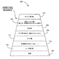
図2は、MTJセル構造200の一例を示し、このセル構造は、所望の熱安定性を低アスペクト比で実現するために適する保磁力の大きい強磁性自由層202を有する。図2のMTJの基本的な層は図1の構造と同様の構造になっている。自由層202は図1の自由層112とは、磁性バイアス層201が自由層202と接触し、かつ磁気結合するように形成されて、自由層202の保磁力を大きくする点で異なる。磁性バイアス層201と自由層202との間の磁気結合は或る大きさに設定され、この大きさの磁気結合によって、自由層202の磁化方向を2つの反対方向の間で、例えば電流をMTJに流し、スピントランスファースイッチング(磁化反転)を利用することにより変更する、または切り替えることができる。或る実施形態では、磁性バイアス層201の磁化方向を、自由層202の磁化容易軸に直交するように配向させて、交換磁界またはループシフト量を小さくする、または最小にすることができる。他の実施形態では、磁性バイアス層201の磁化方向を、自由層202の磁化容易軸に平行になるように配向させることができる。
FIG. 2 shows an example of an
図2に示す構造では、ピンド層111は第1方向または第2方向のいずれかに沿った固定磁化方向を有する。絶縁バリア層130を自由層202とピンド層111との間に形成して、電子が、自由層202とピンド層111との間で、自由層202とピンド層111との間に、かつ絶縁バリア層130にバイアス電圧が印加されている状態でトンネリングを起こすようにする。絶縁バリア層130を形成する金属は、例えばアルミニウム(Al)、ハフニウム(Hf)、ジルコニウム(Zr)、タンタル(Ta)、及びマグネシウム(Mg)とすることができる。更に、異なる金属を利用する種々の窒化物層を使用して絶縁バリア層130を形成することができる。幾つかの例が、アルミニウム窒化物(例えば、AlN)、Ti窒化物(例えば、TiN)、AlTi窒化物(例えば、TiAlN)、及びマグネシウム窒化物である。層111,202,及び114の各々は、2つ以上のサブ層を含む多層構造を有することができる。磁性バイアス層201は反強磁性層または強磁性層とすることができる。
In the structure shown in FIG. 2, the pinned
この構造では、強磁性層111はAFM層113と接触し、かつAFM層113と磁気結合する。強磁性層111は「自由」ではなく、かつこの層の磁化方向がAFM層113によって固定されるので磁化反転することができない。AFM層113は詳細には、強磁性層111の磁化方向をピン止めするように構成される。これに関連して、AFM層113は、3つのパラメータ:すなわちAFM層の層厚tAF、AFM層の異方性定数KAF、及び強磁性層111との結合の程度を示すAFM層の界面交換結合定数Jintによって特徴付けることができる。AFM層113に関するこれらのパラメータは次の条件式を満たす場合、
KAF・tAF>Jint、
AFM層113の磁気異方性が支配的になり、そしてAFM層113は、層111の異方性を、層113と111との間の磁気結合によって磁気的に制御する。この状態では、強磁性層111の磁化方向は、AFM層113の一方向異方性によって固定される。このピン止め状態は、例えばAFM層の膜厚tAFを厚くすることにより、AFM材料の異方性定数KAFを大きくすることにより、または膜厚tAFを厚く、かつ異方性定数KAFを大きくすることにより実現する。ピン止め状態は、AFM層の膜厚tAFが厚く、かつ異方性定数KAFが非常に小さいAFM材料を使用することにより実現することができる。
In this structure, the
K AF · t AF > J int ,
The magnetic anisotropy of the
磁性バイアス層201は、AFM層113とは異なる磁気特性を持つことにより層111をピン止めし、そしてAFM層113とは異なる機能を実現するように構成される。層201及び自由層202は互いに磁気結合するが、自由層202は依然として「自由であり」、そして自由層の磁化方向は、スピントランスファースイッチングに基づいて電流を流すことにより変更することができる。従って、バイアス層201は次の条件式を満たすように構成される:
KAF・tAF<Jint
磁性バイアス層201の膜厚が小さい値に設定される場合、交換バイアス磁界は無視できるほど小さいが、保磁力は、合計異方性エネルギーが自由層202において増大するので、AFM層の膜厚とともに増大する。従って、磁性バイアス層201は、自由層202の異方性磁界を大きくするように構成される。種々の実施形態では、磁性バイアス層201のAFM材料は、ブロッキング温度をMTJセルの動作温度よりも高くし、界面交換結合定数Jintを大きくし、そして異方性定数KAFを適度に大きくするように選択される。反強磁性材料の場合、ネール温度(Neel temperature)がブロッキング温度(冷却過程で磁化が固定される温度)となる。強磁性材料の場合、当該材料のキューリー温度(Curie temperature)がブロッキング温度となる。多くのアプリケーションにおいて、磁性バイアス層201の膜厚tAFは一定の値に設定することができる、または変更することができる。従って、他の2つのパラメータKAF及びJintを調整し、そして選択して、条件式KAF・tAF<Jintを満たし、自由層202の異方性磁界または保磁力Hcが磁気セル構造の熱安定性の条件を満たすために十分な大きさとなるようにする。
The
K AF · t AF <J int
When the film thickness of the
Jint及びKAFの値が固定される場合、臨界AFM膜厚はtAFcritical=Jint/KAFと表わされ、そして交換バイアス磁界Hexが2つの動作領域の間で発現する現象を示す指標として使用される。広く使用される2つのAFM材料がIrMn及びPtMnである場合、tAFcriticalに関する推定値はそれぞれ40オングストローム及び80オングストロームであり、この場合、Jint=0.04(IrMn)erg/cm2及び0.08(PtMn)erg/cm2、及びKAF=1×10+5erg/cm3である。実際のデバイス形態では、これらの値は、製造プロセスにおける種々の複雑さに起因して上記推定値から変わり得る。 When the values of J int and K AF are fixed, the critical AFM film thickness is expressed as t AFractive = J int / K AF, and an index indicating a phenomenon in which the exchange bias magnetic field Hex is developed between the two operating regions. Used as. If the two widely used AFM materials are IrMn and PtMn, estimates for t AFrical are 40 Å and 80 Å, respectively, where J int = 0.04 (IrMn) erg / cm 2 and 0. 08 (PtMn) erg / cm 2 and K AF = 1 × 10 +5 erg / cm 3 . In actual device configurations, these values can vary from the above estimates due to various complexities in the manufacturing process.
磁性バイアス層201は、KAF・tAF<Jintで表わされる領域の内部で動作して、十分に大きい保磁力が隣接する自由層202に発生するように構成される。一例として、磁気セル構造が、データを10年間に渡って保持するために必要とされる条件であるKuV/kBT=55を満たす場合、自由層の該当する保磁力は、IrMnから成るAFM層を、Area=0.02μm2,tF=25オングストローム,Ms=1050 emu/cc,A=1:1を満たす磁性バイアス層として使用する場合に約100エルステッドとなる。しかしながら、既存の実験データは、ほとんどの注目に値する保磁力Hcが数十エルステッド内に収まり、かつ普通、Hcが更に、交換バイアス磁界Hexとともに増大することを示唆している。このような状況では、磁性バイアス層を自由層と一緒に使用して自由層の異方性を大きくするには、AFM積層構造及びプロセス加工技術を用いて、交換バイアス磁界Hexを小さくし、かつ保磁力をKAF・tAF<Jintの条件を満たす範囲内で大きくする必要がある。
The
図3Aは、保磁力HcをKAF・tAF<Jintの条件を満たす範囲で大きくするモードを示し、この場合、KAF=1×10+5erg/cm3、tF=25オングストローム,そしてMs=1050 emu/ccである。図3Bは、KAF・tAFを0.01erg/cm2以上にして自由層における保磁力Hcを大きくする必要があるAFM磁性バイアス層(IrMn)の異方性エネルギーを示している。 FIG. 3A shows a mode in which the coercive force Hc is increased within a range satisfying the condition of K AF · t AF <J int , where K AF = 1 × 10 +5 erg / cm 3 , t F = 25 angstroms, and Ms = 1050 emu / cc. FIG. 3B shows the anisotropy energy of the AFM magnetic bias layer (IrMn) that needs to increase the coercive force Hc in the free layer by setting K AF · t AF to 0.01 erg / cm 2 or more.
図2の磁性バイアス層201は種々の構成で用いることができる。例えば、磁性バイアス層201は単一のAFM層により形成することができ、この場合、組成をプロセス条件を制御することによりずらして、Mn含有量がIrMnの場合に50〜95原子%であり、かつPtMnの場合に30〜80原子%となるようにする。層厚は10〜200オングストロームとすることができる。
The
別の例として、磁性バイアス層201は、2つのAFM材料、すなわちAFM1及びAFM1によりそれぞれ形成される2つのAFMサブ層から成る2重層とすることができる、またはAFM1及びAFM2から成る2重層の積層構造とすることができる。各AFMサブ層は10〜200オングストロームの膜厚を有し、かつIrMnまたはPtMnにより形成することができる。例えば、サブ層AFM1では、Mn含有量がIrMnの場合に75〜85原子%であり、そしてPtMnの場合に45〜55原子%である。層厚はIrMnの場合に10〜40オングストロームとし、そしてPtMnの場合に40〜80オングストロームとすることができる。サブ層AFM2では、Mn含有量がIrMnの場合に50〜85原子%または85〜95原子%であり、そしてPtMnの場合に5〜45原子%または55〜80原子%であり、サブ層AFM2の膜厚は調整することができる。
As another example, the
磁性バイアス層201は、非磁性スペーサが2つのAFM層であるAFM1とAFM2との間に配置される(すなわち、AFM1/スペーサ/AFM2)構成の3つの層から成る3重層とすることもできる、または2つ以上の2重層AFM1/スペーサから成る積層構造とすることもできる(スペーサ=Ru,Ta,Cu,NiFeCr,2〜20オングストローム)。
The
これらの例、及び他の例では、AFM1層及びAFM2層は同様の組成及び構造、または異なる組成及び構造を有することができる。2つ以上のサブ層を有する磁性バイアス層では、自由層と界面を接するAFMサブ層は、AFMの臨界層厚よりも薄い膜厚を有するように構成される。この構成によって、磁性バイアス層全体が成長するときの保磁力Hcを高めながら交換バイアス磁界Hexに対する制御性を高めることができる。 In these and other examples, the AFM1 and AFM2 layers can have similar compositions and structures, or different compositions and structures. In the magnetic bias layer having two or more sublayers, the AFM sublayer in contact with the free layer is configured to have a thickness smaller than the critical layer thickness of the AFM. With this configuration, it is possible to improve the controllability with respect to the exchange bias magnetic field Hex while increasing the coercive force Hc when the entire magnetic bias layer is grown.
マグネトロンスパッタリングを使用して磁性バイアス層を形成することができる。別の構成として、IBD(イオンビーム蒸着)を使用するイオンビーム支援堆積プロセスを使用して、層の構造及び組成を変更して、保磁力Hcを高め、かつ交換バイアス磁界Hexを弱めることができる。更に、磁性バイアス層に磁界中でイオンを照射することにより、交換バイアス磁界Hexを弱めながら保磁力Hcを高めることができる。 Magnetron sputtering can be used to form the magnetic bias layer. Alternatively, an ion beam assisted deposition process using IBD (ion beam evaporation) can be used to alter the layer structure and composition to increase the coercivity Hc and weaken the exchange bias field Hex. . Further, by irradiating the magnetic bias layer with ions in a magnetic field, the coercive force Hc can be increased while weakening the exchange bias magnetic field Hex.
種々のAFM材料を使用して、磁性バイアス層201全体の一つ以上のサブ層を構成することができる。例えば、次のAFM材料の内のいずれかを使用する、または次のAFM材料の内の2つ以上のいずれかの材料の組み合わせを使用することができる:(1)金属AFM材料:IrMn,PtMn,PtPdMn,NiMn,FeMn(Rh),CrMn,FeNiMn,CoMn,RhMn,CrMn(Pt,Cu,Rh,Pd,Ir,Ni,Co,Ti),及びCrAl;(2)酸化物AFM材料:Ni(Fe)O,Fe(Co)O,Co(Fe)O,NiFe(Co)O,CrO;及び(3)FeS。更に、磁性バイアス層201の各AFM材料は、TbCo,DyCo,TbFe,TbFeCo,CoFeO,FeO,及び(Mn,Zn)FeOのような2つ以上の強磁性材料の内の一つの材料、またはこれらの強磁性材料の組み合わせに置き換えることもできる。上の組成化学式では、()内の元素は含有量が少ない元素を表わす。例えば、Fe(Co)Oでは、Coの含有量がFeの含有量よりも少ない。
Various AFM materials can be used to construct one or more sublayers of the entire
CMOS構造及び製造におけるビア処理では、重なりのルールが課されるので、磁気セルのアスペクト比及びサイズが制限を受ける。MTJセルに磁性バイアス層を使用することにより、自由層の熱安定性を高めることができ、かつ安定なMTJセルをCMOSの微細化限界内で形成することができる。自由層は薄い膜厚、及び小さい磁気モーメントを有するように設計して、スピントランスファー効果に基づいて自由層の磁化方向を切り替えるために必要なスピントランスファースイッチングによる電流密度を小さくすることができる。磁性バイアス層を設けることにより、このような薄い自由層に高い保磁力及び所望の熱安定性を持たせることができる。 In CMOS processing and via processing in manufacturing, overlapping rules are imposed, which limits the aspect ratio and size of the magnetic cell. By using a magnetic bias layer in the MTJ cell, the thermal stability of the free layer can be increased, and a stable MTJ cell can be formed within the CMOS miniaturization limit. The free layer can be designed to have a thin film thickness and a small magnetic moment, so that the current density by spin transfer switching required for switching the magnetization direction of the free layer based on the spin transfer effect can be reduced. By providing a magnetic bias layer, such a thin free layer can have high coercive force and desired thermal stability.
一旦、MTJセルのサイズ及びアスペクト比を小さくして、寸法200nmよりも小さくする、または100nm未満とすると、このような小さなMTJセルは熱的に不安定になり易く、かつ磁区構造の磁壁の影響、及び漏洩磁界による影響を受け易くなる。磁壁の影響は、スピンカーリングが生じる、またはスピン渦を引き起こすことによりスピン配向が変化し易くなるように作用する。スピン配向が変化することにより、磁気セルの磁気特性が劣化し、そして情報記憶のデータエラーレートが大きくなる。磁性バイアス層を使用して種々の実施形態におけるこれらの問題を解決することができ、磁性バイアス層と自由層との間で起きる異方性エネルギーに及ぼす強磁性交換相互作用により、スピンが磁性バイアス層の磁化容易軸に沿って配向して、磁気セルの磁気特性を向上させる。 Once the size and aspect ratio of the MTJ cell is reduced to a size smaller than 200 nm or less than 100 nm, such a small MTJ cell is likely to be thermally unstable and is affected by the domain wall of the domain structure. And is susceptible to the influence of a leakage magnetic field. The influence of the domain wall acts so that spin orientation is easily changed by causing spin curling or causing spin vortices. As the spin orientation changes, the magnetic characteristics of the magnetic cell deteriorate and the data error rate of information storage increases. A magnetic bias layer can be used to solve these problems in various embodiments, and the spin exchange causes a magnetic bias due to the ferromagnetic exchange interaction on the anisotropic energy that occurs between the magnetic bias layer and the free layer. Orienting along the easy axis of the layer improves the magnetic properties of the magnetic cell.
特に、自由層の保磁力が磁性バイアス層との磁気相互作用によって高まることにより、MTJセルは所望の安定性を熱擾乱及び漏洩磁界に対して、セルの形状異方性を利用することなく実現することができる。従って、セルの形状異方性の度合いが小さい場合、例えばセルをCMOS処理を用いて形成して、セルが約100nmの寸法を有するようになる場合、磁性バイアス層を使用することによって、MTJセルを、CMOSプロセス技術で達成される低アスペクト比を満たすように設計し、そして形成することができる。このような背景から、磁気セルの形状またはアスペクト比はMTJセルの制約要素ではなくなる。従って、磁性バイアス層を使用することによって、セル設計及びレイアウトを容易にすることができる。更に、自由層の保磁力を所望の大きさに、磁性バイアス層の異方性を、構造及びプロセスを制御して調整することにより設定することができる。この調整は、CMOS処理において行なわれる各セルのアスペクト比に対する制御よりも、相対的に容易に、かつ均一性及びプロセスマージンが改善されるように行なうことができる。 In particular, the MTJ cell achieves the desired stability against thermal disturbances and leakage magnetic fields without using the cell shape anisotropy by increasing the coercivity of the free layer due to the magnetic interaction with the magnetic bias layer. can do. Therefore, when the degree of shape anisotropy of the cell is small, for example, when the cell is formed using CMOS processing and the cell has a dimension of about 100 nm, the MTJ cell is formed by using the magnetic bias layer. Can be designed and formed to meet the low aspect ratios achieved with CMOS process technology. Against this background, the shape or aspect ratio of the magnetic cell is no longer a limiting element of the MTJ cell. Therefore, cell design and layout can be facilitated by using the magnetic bias layer. Furthermore, the coercivity of the free layer can be set to a desired magnitude, and the anisotropy of the magnetic bias layer can be set by controlling the structure and process. This adjustment can be performed relatively easily and so as to improve the uniformity and the process margin, rather than the control over the aspect ratio of each cell performed in the CMOS processing.
図2の構造における磁性バイアス層以外の層の種々の例について以下に説明する。 Various examples of layers other than the magnetic bias layer in the structure of FIG. 2 will be described below.
1.自由層
自由層(FL)はCo,Fe,Ni,またはこれらの金属の合金であり、これらの金属及び合金は結晶構造を有する、またはボロンによって改質されるアモルファス状態になっている、或いは他のアモルファス形成元素が異なる組成(0〜30原子%)で添加された状態になっている。自由層の飽和磁化は、アモルファス形成元素の組成を変えることにより、400〜1500emu/cm3の範囲に調整することができる。層厚を制御して、出力信号が許容レベルに維持されるようにすることができる(電流誘起磁化反転を最適化しながら)。
1. Free layer The free layer (FL) is Co, Fe, Ni, or alloys of these metals, and these metals and alloys have a crystalline structure or are in an amorphous state modified by boron, or others The amorphous forming elements are added in different compositions (0 to 30 atomic%). The saturation magnetization of the free layer can be adjusted to a range of 400 to 1500 emu / cm 3 by changing the composition of the amorphous forming element. The layer thickness can be controlled so that the output signal is maintained at an acceptable level (while optimizing current-induced magnetization reversal).
自由層は単一層構造または多層構造とすることができる。単一層構造の場合、強磁性材料またはフェリ磁性材料を使用することができる。多層構造の個々の層は、強磁性材料またはフェリ磁性材料のいずれかである複数の磁性材料の組み合わせとする、或いは磁性層及び非磁性層の組み合わせ(2つの強磁性層が非磁性スペーサによって分離される構成の複合反強磁性体のような)とすることができる。スペーサ層をこの複合構造に使用することによって更に、拡散停止層が、反強磁性層に使用されるMn元素がバリア層に拡散する可能性を無くすように作用するという利点が得られる。強磁性層は、Co,CoFe(5〜40%),CoFe(5〜40%)B(5〜30%),CoFe(5〜40%)Ta(5〜30%),NiFe(〜20%),CoPt(5〜40%),CoPd(5〜40%),FePt(5〜40%),Co2Mn(Al,Si),またはCo2(Cr,Fe)(Al,Si)とすることができる。フェリ磁性層は、CoGd(15〜35%)またはFeGd(10〜40%)とすることができる。非磁性スペーサは、Ru,Re,またはCuとすることができる。全ての組成は原子パーセントで表記されている。 The free layer can be a single layer structure or a multilayer structure. In the case of a single layer structure, a ferromagnetic material or a ferrimagnetic material can be used. Each layer of the multilayer structure is a combination of a plurality of magnetic materials, either ferromagnetic materials or ferrimagnetic materials, or a combination of magnetic and nonmagnetic layers (the two ferromagnetic layers are separated by nonmagnetic spacers). Such as a composite antiferromagnet having a structure as described above. The use of a spacer layer in this composite structure further provides the advantage that the diffusion stop layer acts to eliminate the possibility of Mn elements used in the antiferromagnetic layer diffusing into the barrier layer. Ferromagnetic layers are Co, CoFe (5-40%), CoFe (5-40%) B (5-30%), CoFe (5-40%) Ta (5-30%), NiFe (-20%). ), CoPt (5-40%), CoPd (5-40%), FePt (5-40%), Co 2 Mn (Al, Si), or Co 2 (Cr, Fe) (Al, Si). be able to. The ferrimagnetic layer can be CoGd (15-35%) or FeGd (10-40%). The non-magnetic spacer can be Ru, Re, or Cu. All compositions are expressed in atomic percent.
2.ピン層
ピン層(PL)は、Co,Fe,Ni,またはこれらの金属の合金であり、これらの金属及び合金は結晶構造を有する、またはボロンによって改質されるアモルファス状態になっている、或いは他のアモルファス形成元素が異なる組成(0〜30原子%)で添加された状態になっている。ピン層は、単一層構造または多層構造とすることができる。単一層構造の場合、強磁性材料またはフェリ磁性材料を使用することができる。多層構造の個々の層は、強磁性材料またはフェリ磁性材料のいずれかである複数の磁性材料の組み合わせとする、或いは磁性層及び非磁性層の組み合わせ(2つの強磁性層が非磁性スペーサによって分離される構成の複合反強磁性体のような)とすることができる。強磁性層は、Co,CoFe(5〜40%),CoFe(5〜40%)B(5〜30%),CoFe(5〜40%)Ta(5〜30%),NiFe(〜20%),CoPt(5〜40%),CoPd(5〜40%),FePt(5〜40%),Co2Mn(Al,Si),またはCo2(Cr,Fe)(Al,Si)とすることができる。フェリ磁性層は、CoGd(15〜35%)またはFeGd(10〜40%)とすることができる。非磁性スペーサは、Ru,Re,またはCuとすることができる。全ての組成は原子パーセントで表記されている。
2. Pinned layer The pinned layer (PL) is Co, Fe, Ni, or an alloy of these metals, and these metals and alloys have a crystalline structure or are in an amorphous state modified by boron, or Other amorphous forming elements are added in different compositions (0 to 30 atomic%). The pinned layer can be a single layer structure or a multilayer structure. In the case of a single layer structure, a ferromagnetic material or a ferrimagnetic material can be used. Each layer of the multilayer structure is a combination of a plurality of magnetic materials, either ferromagnetic materials or ferrimagnetic materials, or a combination of magnetic and nonmagnetic layers (the two ferromagnetic layers are separated by nonmagnetic spacers). Such as a composite antiferromagnet having a structure as described above. Ferromagnetic layers are Co, CoFe (5-40%), CoFe (5-40%) B (5-30%), CoFe (5-40%) Ta (5-30%), NiFe (-20%). ), CoPt (5-40%), CoPd (5-40%), FePt (5-40%), Co 2 Mn (Al, Si), or Co 2 (Cr, Fe) (Al, Si). be able to. The ferrimagnetic layer can be CoGd (15-35%) or FeGd (10-40%). The non-magnetic spacer can be Ru, Re, or Cu. All compositions are expressed in atomic percent.
3.バリア層
トンネルバリア層は、AlO(40〜70%),MgO(30〜60%),AlO(40〜70%)N(2〜30%),AlN(30〜60%),及びAl(Zr,Hf,Ti,Ta)Oから成る単一層、または上に挙げた膜から成る多層構造とすることができ、これらの層または膜は結晶構造を有する、またはアモルファス状態になっている。5オングストローム〜40オングストロームの範囲の膜厚を有するバリア層は、元の金属開始材料を堆積させ、次に堆積膜を自然酸化及び/又はプラズマ酸化を使用して酸化することにより、または元の酸化物開始材料を、トンネル電流がバリアを流れるようにrfスパッタリングすることにより処理される。バリアの抵抗−面積の積の範囲は10〜100Ω−μm2である。バリアと自由層との間だけでなく、バリアとピンド層との間の界面の構造を最適化して電子の最大のスピン偏極率(偏極率>40%)だけでなく、最大のトンネル磁気抵抗(TMR)値(例えば、TMR>20%)を実現する。
3. Barrier layer The tunnel barrier layer comprises AlO (40-70%), MgO (30-60%), AlO (40-70%) N (2-30%), AlN (30-60%), and Al (Zr , Hf, Ti, Ta) O can be a single layer or a multilayer structure of the films listed above, which have a crystalline structure or are in an amorphous state. A barrier layer having a thickness in the range of 5 angstroms to 40 angstroms can be obtained by depositing the original metal starting material and then oxidizing the deposited film using natural and / or plasma oxidation, or the original oxidation. The material starting material is processed by rf sputtering so that the tunneling current flows through the barrier. The resistance-area product range of the barrier is 10-100 Ω-μm 2 . Optimize the structure of the interface between the barrier and the pinned layer as well as between the barrier and the free layer to maximize not only the maximum spin polarization (polarization> 40%) but also the maximum tunneling magnetism A resistance (TMR) value (for example, TMR> 20%) is realized.
4.スペーサ層
スピンバルブセルでは、MTJセルに関して上に説明したバリア層130は、非磁性金属スペーサ層によって置き換えられる。スペーサ材料の例として、Cu,Ag,Pt,Ru,Re,Rh,Ta,Ti,2つ以上のこれらの金属の組み合わせ、またはこれらの金属の合金を挙げることができる。非磁性スペーサ層は、上に挙げた金属の内の一つ以上の金属を、ナノ酸化物(NOL)層または電流閉じ込め層を挿入する形でこれらの層と組み合わせることにより形成することができる。或る実施形態では、非磁性スペーサは、まず、元の金属開始材料を堆積させ、次に堆積膜を自然酸化及び/又はプラズマ酸化を使用して酸化することにより、または元の金属開始材料をrfスパッタリングすることにより形成することができる。金属開始材料には、ピン層材料または自由層材料と同様の材料を使用することができ、このような材料として、CoFe,CoFeB,及びCoFeNiBのような磁性材料、及びAl,Ta,Ru,及びTiのような非磁性材料を挙げることができる。電流閉じ込め層は、例えばCu/CoFe,FeSi,Al,Ta,Ru,またはTi/NOL/Cuとすることができる。
4). Spacer Layer In the spin valve cell, the
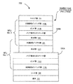
図2の磁性バイアス層を有するMTJセルには、「bottom MTJ(ボトムMTJ)」構造を使用し、この構造では、強磁性ピンド層111がバリア層130と基板101との間に配置される。別の構成として、自由層202及び当該自由層の磁性バイアス層201は「top MTJ(トップMTJ)」構造においては、バリア層130の下に、かつ基板101の上方に配置することができる。図4は、磁性バイアス層201をシード層(群)102の上に直接成長させる構成のMTJの一例400を示している。
The MTJ cell having the magnetic bias layer of FIG. 2 uses a “bottom MTJ (bottom MTJ)” structure, in which the ferromagnetic pinned
更に複雑な構造は、磁性バイアス層を有する上に説明したMTJを基本にして構成することができる。図5は、デュアルMTJ構造500を示し、この構造では、2つのMTJ510及び520を互いに対して積層し、そして共通磁性バイアス層501を共有する。この例では、第1MTJ510は、シード層102の上に直接形成されるAFM(反強磁性)ピンニング層113Aを有し、そしてMTJ510の他の層、すなわちピンド層111A、バリア層130A、自由層511、及び磁性バイアス層501は、AFM層113Aの上に順番に配置される。MTJ510の磁性バイアス層501は、MTJ520の磁性バイアス層でもあり、MTJ520は、自由層521、バリア層130B、ピンド層111B、及びAFMピンニング層113Bを含み、これらの層は、磁性バイアス層501の上に順番に配置される。次に、一つ以上のキャップ層114をMTJ520の上に形成する。
More complex structures can be constructed based on the MTJ described above having a magnetic bias layer. FIG. 5 shows a
上に説明した磁気セル構造では、自由層の磁化方向をスピントランスファー効果を利用して反転させるために使用される電流は、自由層の横方向寸法を小さくすることにより小さくすることができる。反転電流を小さくすることにより、メモリセルの消費電力を小さくし、かつ高集積メモリセル構造における熱放散問題を軽減することができる。バイアス層を設けて薄い自由層の熱安定性を高める他に、セル形状を、スピントランスファートルクによる書き込み電流密度を小さくするように設計することができる。 In the magnetic cell structure described above, the current used to reverse the magnetization direction of the free layer using the spin transfer effect can be reduced by reducing the lateral dimension of the free layer. By reducing the inversion current, the power consumption of the memory cell can be reduced and the heat dissipation problem in the highly integrated memory cell structure can be reduced. In addition to providing a bias layer to increase the thermal stability of the thin free layer, the cell shape can be designed to reduce the write current density due to the spin transfer torque.
図6A及び6Bは、図2のセル構造を、自由層の寸法を小さくした形で用いて2つのセル形状を設計した様子を示している。図6Aでは、各セルの積層構造601の側面形状を傾斜させて、または傾けて自由層202の横方向寸法を小さくしている。図6Bでは、各セルの積層構造602を逆T字型の形状にして、メサトップに自由層202及び磁性バイアス層201を形成し、そしてボトムにバリア層130、ピンド層111、及びAFM層113、シード層102を形成する。メサトップの寸法をボトムの寸法よりも小さくして、メサトップに形成される自由層の横方向寸法を小さくする。同様に、図7A及び7Bは、図5のセル構造を、自由層の寸法を小さくした形で用いて2つのセル形状を設計した様子を示している。
FIGS. 6A and 6B show the design of two cell shapes using the cell structure of FIG. 2 with a reduced free layer size. In FIG. 6A, the lateral dimension of the
図6A及び7Aに示す上述の傾斜側壁形状は、処理中にマスク層の傾斜を利用することにより得られ、そして図6B及び7Bに示す逆T字型の形状は、側壁スペーサプロセスを使用することにより得られる。 The above-described slanted sidewall shape shown in FIGS. 6A and 7A is obtained by utilizing the slope of the mask layer during processing, and the inverted T shape shown in FIGS. 6B and 7B uses a sidewall spacer process. Is obtained.
MTJ構造に関して上に示した例は、スピンバルブ構造によって置き換えることもでき、この置き換えは、MTJバリア絶縁層を、非磁性金属スペーサ層に置き換えることにより行なわれる。図5では、例えば図示のデュアル構造はデュアルスピンフィルタ(dual spin filter)とすることができ、デュアルスピンフィルタでは、スピンバルブ及びMTJを、2つのバリアの一方を非磁性スペーサ層に置き換えることにより、互いの上に積層させる。 The example shown above for the MTJ structure can also be replaced by a spin valve structure, which is done by replacing the MTJ barrier insulating layer with a non-magnetic metal spacer layer. In FIG. 5, for example, the dual structure shown can be a dual spin filter, where the spin valve and MTJ are replaced by a non-magnetic spacer layer by replacing one of the two barriers. Laminate on top of each other.
磁性バイアス層を有する上述のMTJセルを利用するMRAMメモリデバイスは、ビットをセルに記憶するためにスピントランスファースイッチング(スピントランスファーによる磁化反転)を利用するように構成することができる。行選択及び列選択を行ない、かつワードライン及びビットラインを含む回路要素がMRAMメモリデバイスに組み込まれる。データを記憶する偏極電流を流す書き込み電流源、及び読み出しセンス電流を供給する読み出し電流源もメモリデバイスに組み込まれる。このようなメモリデバイスにおけるスピントランスファースイッチングは種々の構成で行なうことができる。スピントランスファーに関する現時点での情報は、Journal of Magnetism and Magnetic Mterials, vol. 159, p. L1−L5 (1996)に掲載されたJ. C. Slonczewskiによる「磁気多層の電流駆動励磁」と題する論文、Phys. Rev. B, Vol. 54, p. 9353 (1996)に掲載されたL. Bergerによる「電流を磁気多層膜に流すことによるスピン波の励起」と題する論文、及びAppl. Phys. Lett., vol. 77, No. 23, p. 3809−3811 (2000)に掲載されたF. J Albert, J. A. Katine and R. A. Burhmanによる「Co薄膜ナノ磁石のスピン偏極電流による磁化反転」と題する論文に記載されている。しかしながら、スピントランスファーは、上記参考文献に記載される技術に示される構成以外の他の構成で利用することができる。 An MRAM memory device using the above-described MTJ cell with a magnetic bias layer can be configured to use spin transfer switching (magnetization reversal by spin transfer) to store bits in the cell. Circuit elements that perform row selection and column selection and that include word lines and bit lines are incorporated into the MRAM memory device. A write current source for supplying a polarization current for storing data and a read current source for supplying a read sense current are also incorporated in the memory device. Spin transfer switching in such a memory device can be performed in various configurations. Current information regarding spin transfer can be found in Journal of Magnetics and Magnetic Materials, vol. 159, p. L1-L5 (1996). C. A paper entitled “Current-driven excitation of magnetic multilayers” by Slonkzewski, Phys. Rev. B, Vol. 54, p. 9353 (1996). Berger's paper entitled “Excitation of spin waves by passing current through a magnetic multilayer”, and Appl. Phys. Lett. , Vol. 77, no. 23, p. 3809-3811 (2000). J Albert, J.A. A. Katine and R.C. A. It is described in a paper entitled “Reversal of magnetization by spin-polarized current of Co thin film nanomagnet” by Burhman. However, the spin transfer can be used in configurations other than the configuration shown in the technique described in the above-mentioned reference.
上記参考文献に基づいて、スピントランスファー効果は、強磁性金属−常伝導金属多層膜のスピン依存電子輸送機構により生じる。スピン偏極電流が磁性多層構造を、これらの層に直交する方向に流れる場合、強磁性層に流れ込む電子のスピン角運動量が強磁性層と常伝導金属層との界面近傍の強磁性層の磁気モーメントと相互作用する。この相互作用を通して、電子のスピン角運動量の一部が強磁性層の磁気モーメントへと受け渡される。その結果、スピン偏極電流によって、電流密度が十分に大きい場合(約107〜108A/cm2)に、かつ直交電流によって生じる螺旋状磁場の影響が大きくならないくらいに多層膜の寸法が小さい(約200ナノメートル未満)場合に、強磁性層の磁化方向を切り替え(反転させ)ることができる。更に、自由層の磁化方向を変更するための磁化反転電流を小さくするために、強磁性層を十分薄くする、例えば好ましくは或る実施形態では、Coの場合に約10ナノメートル未満とする必要がある。薄い自由層は磁性バイアス層を設けない状態では、保磁力が小さく、かつ大きな反転電流を必要とする厚い自由層よりも安定性が低い。磁性バイアス層を使用することにより、自由層を薄くして反転電流を小さくすることができるとともに、熱擾乱及び漏洩磁界に対して十分大きな保磁力を維持することができる。 Based on the above references, the spin transfer effect is caused by the spin-dependent electron transport mechanism of the ferromagnetic metal-normal metal multilayer. When the spin-polarized current flows through the magnetic multilayer structure in a direction perpendicular to these layers, the spin angular momentum of electrons flowing into the ferromagnetic layer causes the magnetic properties of the ferromagnetic layer near the interface between the ferromagnetic layer and the normal metal layer. Interact with moments. Through this interaction, part of the spin angular momentum of the electrons is transferred to the magnetic moment of the ferromagnetic layer. As a result, when the current density is sufficiently large due to the spin-polarized current (about 10 7 to 10 8 A / cm 2 ), the dimension of the multilayer film is not increased so that the influence of the helical magnetic field generated by the orthogonal current does not increase. When it is small (less than about 200 nanometers), the magnetization direction of the ferromagnetic layer can be switched (reversed). In addition, the ferromagnetic layer should be thin enough to reduce the magnetization reversal current for changing the magnetization direction of the free layer, for example, preferably in some embodiments, less than about 10 nanometers in the case of Co. There is. The thin free layer is less stable than the thick free layer, which has a small coercive force and requires a large reversal current, when no magnetic bias layer is provided. By using the magnetic bias layer, the free layer can be thinned to reduce the reversal current, and a sufficiently large coercive force can be maintained against thermal disturbance and leakage magnetic field.
上述したように、種々の磁気構造の例における強磁性自由層は2つ以上の層を含むことができる。このような多層構造の強磁性自由層は、種々の構成で用いることができる。例えば、多層構造の強磁性自由層は、複数の磁性材料の組み合わせを含むことができ、そしてこれらの磁性材料の各々は、強磁性材料またはフェリ磁性材料のいずれかとすることができる。強磁性自由層に関するこのような組み合わせにおける強磁性材料として、Co;Coを含む合金;Fe;Feを含む合金;Ni;またはNiを含む合金を挙げることができる。従って、特定の例では、強磁性自由層に関するこのような組み合わせにおける強磁性材料として、Co;Coを含む合金;Fe;Feを含む合金;Ni;及びNiを含む合金の内の2つ以上を挙げることができる。強磁性自由層に関する組み合わせに適する強磁性合金の幾つかの例として、CoFe,CoFeB,CoFeNiB,CoFeTa,NiFe,CoPt,CoPd,FePt,Co2Mn(Al,Si),及びCo2(Cr,Fe)(Al,Si)を挙げることができる。強磁性自由層に関するフェリ磁性材料は、例えばCoGdまたはFeGdとすることができる。 As mentioned above, the ferromagnetic free layer in the various magnetic structure examples can include more than one layer. Such a multilayered ferromagnetic free layer can be used in various configurations. For example, a multi-layered ferromagnetic free layer can include a combination of a plurality of magnetic materials, and each of these magnetic materials can be either a ferromagnetic material or a ferrimagnetic material. The ferromagnetic material in such a combination for the ferromagnetic free layer can include Co; an alloy containing Co; Fe; an alloy containing Fe; Ni; or an alloy containing Ni. Thus, in particular examples, as a ferromagnetic material in such a combination for the ferromagnetic free layer, Co; an alloy containing Co; Fe; an alloy containing Fe; Ni; and two or more of the alloys containing Ni Can be mentioned. Some examples of ferromagnetic alloys suitable for combination with a ferromagnetic free layer include CoFe, CoFeB, CoFeNiB, CoFeTa, NiFe, CoPt, CoPd, FePt, Co 2 Mn (Al, Si), and Co 2 (Cr, Fe ) (Al, Si). The ferrimagnetic material for the ferromagnetic free layer can be, for example, CoGd or FeGd.
特に、多層構造の強磁性自由層は、磁性層及び非磁性層の組み合わせを含むことができる。一つの特定の例が多層サンドイッチ構造であり、この構造は、2つの強磁性層、及びこれらの2つの強磁性層の間の非磁性スペーサ層を有する。 In particular, the ferromagnetic free layer having a multilayer structure can include a combination of a magnetic layer and a nonmagnetic layer. One particular example is a multilayer sandwich structure, which has two ferromagnetic layers and a nonmagnetic spacer layer between the two ferromagnetic layers.
図8はMTJ構造800の一例を示し、この場合、強磁性自由層積層構造(multilayered free ferromagnetic stack)810は、第1強磁性層811及び第2強磁性層812と、そして2つの強磁性層811と強磁性層812との間の非磁性スペーサ層813と、を有する多層サンドイッチ構造である。非磁性スペーサ層813は、2つの強磁性層811と強磁性層812との間の磁気結合を可能にして、強磁性自由層積層構造810が全体として、一つの強磁性自由層のように動作するように構成され、この強磁性自由層は、電流をMTJに流すことによって磁化反転させることができ、かつMTJの磁性バイアス層201によって安定化させることができる。この強磁性自由層積層構造810を使用して一つの自由層を、図1A,4,5,6A,6B,7A,及び7Bに示す例のような他の構造に用いることもできる。磁気メモリデバイスとして使用される場合、バリア層130と接触する第1強磁性層811は主として記憶層として機能して、記録ビットを2つの方向のいずれかの方向として記憶する。
FIG. 8 shows an example of an
強磁性自由層積層構造810は、単一材料しか含まない一つの自由層では実現することが難しい多数の利点をもたらすように構成することができる。例えば、非磁性スペーサ層813は、拡散バリア層として機能して、堆積後アニール処理を行なっている間の不所望の拡散及び結晶配向の進行を阻止することができる。
The ferromagnetic
別の例として、強磁性材料は磁歪現象を起こす、すなわち材料の寸法及び形状が磁界とともに変化する。磁歪現象は、一つの理由として、MTJアレイにおいてセルの位置を一つのMTJセルから別のMTJセルに変えたときにセルの形状または寸法に変化が生じると必ず、MTJセルの動作が変化してデバイス性能が低下するので望ましくない。2つの強磁性層811及び812を、強磁性自由層積層構造810の多層サンドイッチ構造に使用することにより、多層サンドイッチ構造を、強磁性自由層積層構造810の多層サンドイッチ構造の全体としての磁歪を小さくするように設計することができる。例えば、2つの強磁性層811及び812の材料は、磁歪がほぼゼロになるように選択することができる。この状態を実現することができない、または難しい場合、2つの強磁性層811及び812の材料は、磁歪を反対方向に生じて、これらの材料の磁歪が、強磁性自由層積層構造810の多層サンドイッチ構造において互いに打ち消し合って、全体としての磁歪がゼロになる、またはほぼゼロになるように選択することができる。
As another example, ferromagnetic materials undergo magnetostriction, i.e., the size and shape of the material changes with the magnetic field. One reason for the magnetostriction phenomenon is that when the cell position or the size of a MTJ cell changes from one MTJ cell to another MTJ cell, the operation of the MTJ cell always changes. This is undesirable because it degrades device performance. By using the two
従って、強磁性自由層積層構造810の多層サンドイッチ構造によって、層811,812、及び813の材料を選択し、そして単一材料の自由層構造では解決することが困難な構造の全体特性を設計するための技術的な柔軟性がもたらされる。
Thus, the multilayer sandwich structure of the ferromagnetic free
強磁性自由層積層構造810における2つの強磁性層811及び812の相対磁化方向は2つの構成で実現することができる。第1の構成は反平行構成であり、この場合、2つの強磁性層811及び812の磁化方向が、2つの強磁性層811及び812が反強磁性結合することによって互いに反対になるように設定される。2つの強磁性層811及び812が反強磁性結合することによって、この反平行構成が維持されるので、2つの層811及び812の磁化方向が一斉に反転する。第2の構成は平行構成であり、この場合、2つの強磁性層811及び812の磁化方向が、2つの強磁性層811及び812が強磁性結合することによって互いに平行になるように設定される。2つの層811及び812が強磁性結合することによって、この平行構成が維持されるので、2つの層811及び812の磁化方向が一斉に切り替えられる(反転する)。これらの2つの構成は異なる。スピントランスファートルク磁化反転が起きる場合、反平行構成では書き込み閾値電流が、平行構成における書き込み閾値電流よりも大きくなり易い。従って、平行構成を、書き込み電流が小さく、従って消費電力が小さい幾つかのデバイスに用いると有利となる。
The relative magnetization directions of the two
2つの強磁性層811及び812が設けられる場合、層811と812との間の非磁性スペーサ層813は、強磁性自由層積層構造810を、2つの構成の内のいずれかの構成に設定するように構成することができる。所定の導電性非磁性材料がスペーサ層813として使用される場合、スペーサ層813の膜厚を制御して、強磁性結合または反強磁性結合のいずれかを生じさせることができる。スペーサ層813が、例えばルテニウムにより形成される場合、反強磁性結合は、Ru層813の膜厚が約3または7、または18、或いは31オングストロームの場合に生じる。Ru層813の膜厚が3〜7オングストローム、または7〜18オングストローム、或いは18〜31オングストロームの場合、強磁性結合が層811と812との間で生じる。
When two
種々の実施形態において、2つの強磁性層811及び812に適する強磁性材料として、例えばCo;Coを含む合金;Fe;Feを含む合金;Ni;またはNiを含む合金を挙げることができる。特定の例では、強磁性材料として、CoFe,CoFeB,CoFeNiB,CoFeTa,NiFe,CoPt,CoPd,FePt,Co2Mn(Al,Si),またはCo2(Cr,Fe)(Al,Si)を挙げることができる。非磁性スペーサ層813は、例えばRu,Re,またはCuとすることができる。強磁性自由層積層構造810を磁気的に安定化させる磁性バイアス層201を設けることによって、磁性バイアス層201、強磁性自由層積層構造810、絶縁バリア層130、及び強磁性ピンド層111を含む各MTJセルをパターニングして、互いに平行な2つの直交方向に沿った寸法のアスペクト比を小さくすることができる。小さいこのアスペクト比を約1に設定してセル密度を高くし、そしてCMOS製造処理のアスペクト比に合わせることができる。
In various embodiments, suitable ferromagnetic materials for the two
強磁性自由層積層構造810の多層サンドイッチ構造の特定の例として、ピンド層130と接触する第1強磁性層811はCoFeXとすることができ、この場合、XはB,P,Si,Nb,Zr,Hf,Ta,及びTiの内の少なくとも一つを含む。磁性バイアス層201と接触する第2強磁性層812は、磁歪がほぼゼロのNiFeまたはNiFeCo合金のような軟磁性材料から成る層とすることができる。第1強磁性層811のCoFeX材料の組成、及び第2強磁性層812の材料の組成を選択して逆の磁歪特性を生じさせ、自由層積層構造810の全体としての磁歪がほぼゼロとなるようにする。所望の材料組成を実現するための一つの方法では、第1強磁性層811のCoFeXにおける元素(すなわち、Co,Fe,及びX)の相対割合、及び第2強磁性層812のNiFeまたはNiFeCoにおける元素の相対割合を制御する。
As a specific example of the multilayer sandwich structure of the ferromagnetic free
非磁性層813を十分薄く形成して、2つの強磁性層811及び812が磁気結合することができるようにする。2つの強磁性層の間のこの磁気結合は、多数の磁気結合機構のいずれかの磁気結合機構、または多数の磁気結合機構の組み合わせとすることができる。このような磁気結合機構の一つの例が、核磁気モーメントを利用する、または伝導電子の相互作用により金属中に局在化したd殻電子のスピンを利用するRKKY(Ruderman−Kittel−Kasuya−Yoshida)的層間結合による強磁性結合である。別の例が、非磁性スペーサ層の界面粗さによって生じる「オレンジピール効果(orange peel)」といわれる静磁気的結合である。第3の例が、非磁性スペーサ層813内に形成されるピンホールのような空間的な不連続による磁気結合である。非磁性スペーサ層813の材料は、Ru,Re,Cu,Taの内のいずれかとする、またはこれらの材料の内のいずれかを含む非磁性合金とすることができる。非磁性層の膜厚はゼロ〜数十オングストロームの範囲である。特定の例として、4オングストローム〜数10オングストロームの薄い非磁性層を使用することができる。
The
磁性バイアス層201は、PtMnのような単一のAFM層により形成することができ、かつ強いピンニング磁界に関連する臨界膜厚よりも薄い膜厚を有することができる。別の構成として、磁性バイアス層201は、非磁性層を間に挿入した構成の多層構造を有することができる。上に説明したように、磁性バイアス層201によって、隣接する強磁性自由層積層構造810の面内異方性、または保磁力を大きくすることができ、更に弱いピンニング磁界を、隣接する強磁性自由層積層構造810に供給することができる。磁性バイアス層201の磁化配向は、隣接する強磁性自由層積層構造810内の弱いピンニング磁界が、トンネルバリア層130の下方のピンド層111の固定磁化方向とは異なる方向に向くように設定することができる。
The
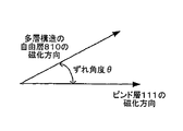
図9は、磁化が弱く固定された強磁性自由層積層構造810とピンド層111との間の磁化方向のずれを示している。強磁性自由層積層構造810の磁化方向が、ピンド層111の磁化方向から角度θだけ異なるように設定される場合、スピントランスファートルクによる書き込み電流により生成される開始トルク値は大きく、かつ角度がランダムな熱擾乱によって生じる変動及び分布を示す場合よりも変動がずっと小さくなる。このようなずれが発生する構造では、STTによる平均書き込み電流が小さくなり、かつ高い書き込み速度(例えば、約nsの書き込み時間を要する)での当該書き込み電流の分布を最小化することができる。種々の実施形態においては、ずれ角度θはゼロ〜180度の間、例えばゼロ〜135度の間の値に設定することができる。このずれ角度は、例えばMTJ膜(または、パターニング済みのデバイス)に2回目のアニールを、ピンド層(PL)の設定(PL/PtMn)に用いる1回目のアニールよりも低い磁界の中で、かつ低い温度で施すことにより実現することができる。
FIG. 9 shows the deviation of the magnetization direction between the ferromagnetic free layer
本出願の明細書は多くの特定要素を含むが、これらの要素は、いずれの発明の技術範囲を制限するものとしても捉えられるべきではない、または請求内容の技術範囲を制限するものとして捉えられるべきではなく、特定の実施形態に固有の特徴についての記述と捉えられるべきである。本明細書において個別の実施形態に関して記載される所定の特徴は、組み合わせることにより単一の実施形態として実現することもできる。逆に、単一の実施形態に関して記載される種々の特徴は、複数の実施形態において個別に、またはいずれかの適切な部分的な組み合わせとして実現することもできる。更に、種々の特徴を、所定の複数の組み合わせで作用するものとして上に記述することができ、かつそのようなものとして初めて請求することもできるが、請求する一つの組み合わせに含まれる一つ以上の特徴は或る場合においては、当該組み合わせから削除することができ、そして請求する当該組み合わせを部分的な一つの組み合わせとする、または部分的な一つの組み合わせの変形とすることができる。 The specification of this application includes many specific elements, which should not be construed as limiting the scope of any invention, or as limiting the scope of the claimed subject matter. It should not be taken as a description of features specific to a particular embodiment. Certain features that are described in this specification in the context of separate embodiments can also be combined and implemented as a single embodiment. Conversely, various features that are described with respect to a single embodiment can also be implemented in multiple embodiments individually or in any suitable subcombination. In addition, various features may be described above as acting in a given plurality of combinations, and may be claimed for the first time as such, but one or more included in a claimed combination. In certain cases can be eliminated from the combination and the claimed combination can be a partial combination or a variation of a partial combination.
幾つかの例についてのみ記述している。この技術分野の当業者であれば、変更、変形、及び機能向上を記載の例に加え得ることが容易に理解できるであろう。 Only a few examples are described. Those skilled in the art will readily understand that changes, modifications, and enhancements can be made to the examples described.
Claims (66)
前記基板上に形成される磁気セルであって、強磁性自由層積層構造と、磁性バイアス層と、強磁性固定層と、絶縁バリア層と、を含む磁気セルと;を備え、:
前記強磁性自由層積層構造は、第1方向と、前記第1方向とほぼ反対の第2方向との間で変更することができる正味の磁化の向きを有し、前記強磁性自由層積層構造は第1及び第2強磁性層と、前記第1強磁性層と前記第2強磁性層との間の非磁性スペーサと、を含み;
前記磁性バイアス層は、前記強磁性自由層積層構造と接触し、かつ磁気結合して前記強磁性自由層積層構造の保磁力を大きくし、そして前記第1方向と、前記第1方向とほぼ反対の前記第2方向との間での前記強磁性自由層積層構造の磁化方向の変更を可能にし;
前記強磁性固定層は、固定磁化方向を有し;
前記絶縁バリア層は、前記強磁性自由層積層構造と前記強磁性固定層との間に形成され、前記絶縁バリア層によって、電子が、前記強磁性自由層積層構造と前記強磁性固定層との間に、かつ前記絶縁バリア層にバイアス電圧が印加された状態で前記強磁性自由層積層構造と前記強磁性固定層との間でトンネリングを起こすようになり、
前記強磁性自由層積層構造は前記磁性バイアス層と前記絶縁バリア層との間に配置される、デバイス。 A substrate;
A magnetic cell formed on the substrate, comprising: a ferromagnetic free layer stack structure; a magnetic bias layer; a ferromagnetic pinned layer; and an insulating barrier layer.
The ferromagnetic free layer stacked structure has a net magnetization direction that can be changed between a first direction and a second direction substantially opposite to the first direction, and the ferromagnetic free layer stacked structure. Includes first and second ferromagnetic layers, and a nonmagnetic spacer between the first and second ferromagnetic layers;
The magnetic bias layer is in contact with the ferromagnetic free layer stacked structure and magnetically coupled to increase the coercivity of the ferromagnetic free layer stacked structure, and the first direction is substantially opposite to the first direction. Allowing a change in the magnetization direction of the ferromagnetic free layer stack structure between the second direction and the second direction;
The ferromagnetic pinned layer has a pinned magnetization direction;
The insulating barrier layer is formed between the ferromagnetic free layer stacked structure and the ferromagnetic pinned layer, and the insulating barrier layer allows electrons to flow between the ferromagnetic free layer stacked structure and the ferromagnetic fixed layer. In the middle, and in a state where a bias voltage is applied to the insulating barrier layer, tunneling occurs between the ferromagnetic free layer stacked structure and the ferromagnetic pinned layer,
The device, wherein the ferromagnetic free layer stack is disposed between the magnetic bias layer and the insulating barrier layer.
第1及び第2反強磁性層と;
前記第1反強磁性層と前記第2反強磁性層との間のスペーサ層と、
を含む、請求項1記載のデバイス。 The magnetic bias layer is:
First and second antiferromagnetic layers;
A spacer layer between the first antiferromagnetic layer and the second antiferromagnetic layer;
The device of claim 1, comprising:
反強磁性層と;
前記反強磁性層と接触するスペーサ層と、
を含む、請求項1記載のデバイス。 The magnetic bias layer is:
An antiferromagnetic layer;
A spacer layer in contact with the antiferromagnetic layer;
The device of claim 1, comprising:
前記反強磁性層と接触する第2スペーサ層と;
前記第2スペーサ層と接触する第2反強磁性層と、
を含む、請求項26記載のデバイス。 The magnetic bias layer further includes:
A second spacer layer in contact with the antiferromagnetic layer;
A second antiferromagnetic layer in contact with the second spacer layer;
27. The device of claim 26, comprising:
前記基板上に形成され、強磁性自由層積層構造と、強磁性固定層と、絶縁バリア層と、を含む磁気セルと、を備え:
前記強磁性自由層積層構造は第1方向と、前記第1方向とはほぼ反対の第2方向との間で変更することができる正味の磁化の向きを有し、前記強磁性自由層積層構造は第1及び第2強磁性層と、前記第1強磁性層と前記第2強磁性層との間の非磁性スペーサと、を含み、前記第1及び第2強磁性層は非磁性スペーサを介して強磁性結合して平行な磁化方向を有し;
前記強磁性固定層は、固定磁化方向を有し;
前記絶縁バリア層は、前記強磁性自由層積層構造と前記強磁性固定層との間に形成され、前記絶縁バリア層によって、電子が、前記強磁性自由層積層構造と前記強磁性固定層との間に、かつ前記絶縁バリア層にバイアス電圧が印加された状態で前記強磁性自由層積層構造と前記強磁性固定層との間でトンネリングを起こすようになる、デバイス。 A substrate;
A magnetic cell formed on the substrate and comprising a ferromagnetic free layer stack structure, a ferromagnetic pinned layer, and an insulating barrier layer:
The ferromagnetic free layer stacked structure has a net magnetization direction that can be changed between a first direction and a second direction substantially opposite to the first direction, and the ferromagnetic free layer stacked structure Includes first and second ferromagnetic layers, and a nonmagnetic spacer between the first and second ferromagnetic layers, and the first and second ferromagnetic layers include nonmagnetic spacers. Have a parallel magnetization direction through ferromagnetic coupling;
The ferromagnetic pinned layer has a pinned magnetization direction;
The insulating barrier layer is formed between the ferromagnetic free layer stacked structure and the ferromagnetic pinned layer, and the insulating barrier layer allows electrons to flow between the ferromagnetic free layer stacked structure and the ferromagnetic fixed layer. A device in which tunneling occurs between the ferromagnetic free layer stacked structure and the ferromagnetic pinned layer with a bias voltage applied to the insulating barrier layer therebetween.
前記強磁性自由層と接触し、かつ磁気結合するように形成されて前記強磁性自由層の保磁力を大きくし、前記第1方向と、前記第1方向とほぼ反対の前記第2方向との間での前記強磁性自由層の磁化方向の変更を可能にする磁性バイアス層と;
ほぼ前記第1方向に沿って固定される磁化方向を有する強磁性固定層と;
前記強磁性自由層と前記強磁性固定層との間に形成される絶縁バリア層であって、電子が、前記強磁性自由層と前記強磁性固定層との間に、かつ前記絶縁バリア層にバイアス電圧が印加された状態で前記強磁性自由層と前記強磁性固定層との間でトンネリングを起こす、絶縁バリア層と、を備え;
前記強磁性自由層は前記磁性バイアス層と前記絶縁バリア層との間に配置される、デバイス。 A ferromagnetic free layer having a magnetization direction that can be changed between a first direction and a second direction substantially opposite to the first direction;
The ferromagnetic free layer is formed so as to be in contact with and magnetically coupled with the ferromagnetic free layer to increase the coercive force of the ferromagnetic free layer, and the first direction and the second direction substantially opposite to the first direction. A magnetic bias layer that allows the magnetization direction of the ferromagnetic free layer to change between;
A ferromagnetic pinned layer having a magnetization direction fixed substantially along the first direction;
An insulating barrier layer formed between the ferromagnetic free layer and the ferromagnetic pinned layer, wherein electrons are between the ferromagnetic free layer and the ferromagnetic pinned layer and in the insulating barrier layer. An insulating barrier layer that causes tunneling between the ferromagnetic free layer and the ferromagnetic pinned layer with a bias voltage applied;
The device, wherein the ferromagnetic free layer is disposed between the magnetic bias layer and the insulating barrier layer.
第1及び第2反強磁性層と;
前記第1反強磁性層と前記第2反強磁性層との間のスペーサ層と、
を含む、請求項41記載のデバイス。 The magnetic bias layer is:
First and second antiferromagnetic layers;
A spacer layer between the first antiferromagnetic layer and the second antiferromagnetic layer;
42. The device of claim 41, comprising:
反強磁性層と;
前記反強磁性層と接触するスペーサ層と、
を含む、請求項41記載のデバイス。 The magnetic bias layer is:
An antiferromagnetic layer;
A spacer layer in contact with the antiferromagnetic layer;
42. The device of claim 41, comprising:
前記磁性バイアス層と接触し、かつ磁気結合することにより変更可能な磁化方向、及び大きな保磁力を有する第2強磁性自由層と;
前記固定磁化方向を有する第2強磁性固定層と;そして
前記第2強磁性自由層と前記第2強磁性固定層との間に形成される第2絶縁バリア層と、を備え、
前記第2絶縁バリア層によって、電子が、前記第2強磁性自由層と前記第2強磁性固定層との間に、かつ前記第2絶縁バリア層にバイアス電圧が印加された状態で前記第2強磁性自由層と前記第2強磁性固定層との間でトンネリングを起こすようになる、請求項41記載のデバイス。 In addition:
A second ferromagnetic free layer having a large coercivity and a magnetization direction that can be changed by being in contact with and magnetically coupled to the magnetic bias layer;
A second ferromagnetic fixed layer having the fixed magnetization direction; and a second insulating barrier layer formed between the second ferromagnetic free layer and the second ferromagnetic fixed layer,
The second insulating barrier layer causes electrons to flow between the second ferromagnetic free layer and the second ferromagnetic fixed layer and with the bias voltage applied to the second insulating barrier layer. 42. The device of claim 41, wherein the device becomes tunneled between a ferromagnetic free layer and the second ferromagnetic pinned layer.
前記磁性バイアス層と接触し、かつ磁気結合することにより変更可能な磁化方向、及び大きな保磁力を有する第2強磁性自由層と;
前記固定磁化方向を有する第2強磁性固定層と;
前記第2強磁性自由層と前記第2強磁性固定層との間に形成されて、前記第2強磁性自由層及び前記第2強磁性固定層を有するスピンバルブを構成する非磁性スペーサ層と、
を備える請求項41記載のデバイス。 In addition:
A second ferromagnetic free layer having a large coercivity and a magnetization direction that can be changed by being in contact with and magnetically coupled to the magnetic bias layer;
A second ferromagnetic pinned layer having the pinned magnetization direction;
A nonmagnetic spacer layer formed between the second ferromagnetic free layer and the second ferromagnetic pinned layer and constituting a spin valve having the second ferromagnetic free layer and the second ferromagnetic pinned layer; ,
42. The device of claim 41, comprising:
前記強磁性自由層と接触し、かつ磁気結合して前記強磁性自由層の磁化方向の変更を可能にしながら、前記強磁性自由層の保磁力を大きくする磁性バイアス層を設ける工程と、を含み、
前記強磁性自由層は前記磁性バイアス層と前記絶縁バリア層との間に配置される、方法。 A magnetic comprising: a ferromagnetic free layer having a changeable magnetization direction; a ferromagnetic fixed layer having a fixed magnetization direction; and an insulating barrier layer formed between the ferromagnetic free layer and the ferromagnetic fixed layer. A step of providing a tunnel junction, wherein the insulating barrier layer allows electrons to be applied between the ferromagnetic free layer and the ferromagnetic pinned layer and with a bias voltage applied to the insulating barrier layer. Causing tunneling between the free layer and the ferromagnetic pinned layer;
Providing a magnetic bias layer that is in contact with the ferromagnetic free layer and magnetically coupled to change the magnetization direction of the ferromagnetic free layer while increasing the coercive force of the ferromagnetic free layer. ,
The method, wherein the ferromagnetic free layer is disposed between the magnetic bias layer and the insulating barrier layer.
前記強磁性自由層と接触し、かつ磁気結合するように形成されて前記強磁性自由層の保磁力を、前記強磁性自由層の磁化方向を固定することなく大きくする磁性バイアス層であって、K・t<Jを満たす層厚t、異方性定数K、及び界面交換結合定数Jを有する、磁性バイアス層と;
所定方向に沿って固定される磁化方向を有する強磁性ピンド層と;
前記強磁性ピンド層と接触し、かつ磁気結合して前記強磁性ピンド層の磁化方向を所定方向に沿って固定するように作用する反強磁性ピンニング層であって、K’・t’>J’を満たす層厚t’、異方性定数K’、及び界面交換結合定数J’を有する、反強磁性ピンニング層と;
前記強磁性自由層と前記強磁性ピンド層との間に形成される中間層と;を備え、
前記強磁性自由層は前記磁性バイアス層と前記中間層との間に配置される、デバイス。 A ferromagnetic free layer having a changeable magnetization direction;
A magnetic bias layer formed in contact with the ferromagnetic free layer and magnetically coupled to increase the coercive force of the ferromagnetic free layer without fixing the magnetization direction of the ferromagnetic free layer; A magnetic bias layer having a layer thickness t satisfying K · t <J, an anisotropy constant K, and an interface exchange coupling constant J;
A ferromagnetic pinned layer having a magnetization direction fixed along a predetermined direction;
An antiferromagnetic pinning layer which is in contact with the ferromagnetic pinned layer and acts to magnetically couple and fix the magnetization direction of the ferromagnetic pinned layer along a predetermined direction, and K ′ · t ′> J An antiferromagnetic pinning layer having a layer thickness t satisfying ', an anisotropy constant K', and an interface exchange coupling constant J ';
An intermediate layer formed between the ferromagnetic free layer and the ferromagnetic pinned layer;
The device, wherein the ferromagnetic free layer is disposed between the magnetic bias layer and the intermediate layer.
Applications Claiming Priority (3)
| Application Number | Priority Date | Filing Date | Title |
|---|---|---|---|
| US11/232,356 US7777261B2 (en) | 2005-09-20 | 2005-09-20 | Magnetic device having stabilized free ferromagnetic layer |
| US11/498,294 US7973349B2 (en) | 2005-09-20 | 2006-08-01 | Magnetic device having multilayered free ferromagnetic layer |
| PCT/US2006/036572 WO2007035786A2 (en) | 2005-09-20 | 2006-09-19 | Magnetic devices having stabilized free ferromagnetic layer or multilayered free ferromagnetic layer |
Publications (1)
| Publication Number | Publication Date |
|---|---|
| JP2009509357A true JP2009509357A (en) | 2009-03-05 |
Family
ID=39420744
Family Applications (1)
| Application Number | Title | Priority Date | Filing Date |
|---|---|---|---|
| JP2008532331A Pending JP2009509357A (en) | 2005-09-20 | 2006-09-19 | Magnetic element having stabilized ferromagnetic free layer or ferromagnetic free layer laminated structure |
Country Status (6)
| Country | Link |
|---|---|
| US (1) | US7973349B2 (en) |
| EP (1) | EP1935029A4 (en) |
| JP (1) | JP2009509357A (en) |
| KR (1) | KR20080070812A (en) |
| TW (1) | TW200713648A (en) |
| WO (1) | WO2007035786A2 (en) |
Cited By (11)
| Publication number | Priority date | Publication date | Assignee | Title |
|---|---|---|---|---|
| WO2011099476A1 (en) * | 2010-02-10 | 2011-08-18 | 株式会社日立製作所 | Ferromagnetic tunnel junction element |
| KR101311128B1 (en) * | 2012-01-25 | 2013-09-25 | 인하대학교 산학협력단 | spin transfer torque magnetic random access memory |
| US8804410B2 (en) | 2011-08-16 | 2014-08-12 | Samsung Electronics Co., Ltd. | Stacked MRAM device and memory system having the same |
| US8947914B2 (en) | 2011-03-18 | 2015-02-03 | Samsung Electronics Co., Ltd. | Magnetic tunneling junction devices, memories, electronic systems, and memory systems, and methods of fabricating the same |
| JP2015515126A (en) * | 2012-03-05 | 2015-05-21 | ヘルムホルツ−ツェントルム ベルリン フュア マテリアリエン ウントエナギー ゲゼルシャフト ミット ベシュレンクテル ハフツングHelmholtz−Zentrum Berlin fuer Materialien und Energie GmbH | Spin valve |
| US9715915B2 (en) | 2014-10-30 | 2017-07-25 | Samsung Electronics Co., Ltd. | Magneto-resistive devices including a free layer having different magnetic properties during operations |
| JPWO2016159017A1 (en) * | 2015-03-31 | 2018-02-01 | 国立大学法人東北大学 | Magnetoresistive element, magnetic memory device, manufacturing method, operating method, and integrated circuit |
| JP2018522404A (en) * | 2015-06-05 | 2018-08-09 | アレグロ・マイクロシステムズ・エルエルシー | Spin valve magnetoresistive element with improved response to magnetic field |
| CN108780779A (en) * | 2016-06-10 | 2018-11-09 | Tdk株式会社 | Exchange biased utilization type magnetization inversion element, exchange biased utilization type magneto-resistance effect element, exchange biased utilization type magnetic memory, non-volatile logic circuit and magnetic neuron element |
| WO2019203454A1 (en) * | 2018-04-17 | 2019-10-24 | 고려대학교 산학협력단 | Magnetic device |
| JP7202267B2 (en) | 2019-08-06 | 2023-01-11 | 株式会社日立ハイテク | Magnetoresistive element and magnetoresistive device |
Families Citing this family (122)
| Publication number | Priority date | Publication date | Assignee | Title |
|---|---|---|---|---|
| WO2005004152A1 (en) * | 2003-07-03 | 2005-01-13 | Fujitsu Limited | Magnetic head slider and method of manufacturing the head slider |
| US7576956B2 (en) * | 2004-07-26 | 2009-08-18 | Grandis Inc. | Magnetic tunnel junction having diffusion stop layer |
| US7436636B2 (en) * | 2004-11-10 | 2008-10-14 | Hitachi Global Storage Technologies Netherlands B.V. | Dual CPP GMR sensor with in-stack bias structure |
| US7411765B2 (en) * | 2005-07-18 | 2008-08-12 | Hitachi Global Storage Technologies Netherlands B.V. | CPP-GMR sensor with non-orthogonal free and reference layer magnetization orientation |
| US8130474B2 (en) * | 2005-07-18 | 2012-03-06 | Hitachi Global Storage Technologies Netherlands B.V. | CPP-TMR sensor with non-orthogonal free and reference layer magnetization orientation |
| US7777261B2 (en) * | 2005-09-20 | 2010-08-17 | Grandis Inc. | Magnetic device having stabilized free ferromagnetic layer |
| US7859034B2 (en) * | 2005-09-20 | 2010-12-28 | Grandis Inc. | Magnetic devices having oxide antiferromagnetic layer next to free ferromagnetic layer |
| US7430135B2 (en) * | 2005-12-23 | 2008-09-30 | Grandis Inc. | Current-switched spin-transfer magnetic devices with reduced spin-transfer switching current density |
| US20070246787A1 (en) * | 2006-03-29 | 2007-10-25 | Lien-Chang Wang | On-plug magnetic tunnel junction devices based on spin torque transfer switching |
| JP2008041163A (en) * | 2006-08-04 | 2008-02-21 | Hitachi Global Storage Technologies Netherlands Bv | Current perpendicular-to-plane magnetoresistance effect head |
| US7851840B2 (en) * | 2006-09-13 | 2010-12-14 | Grandis Inc. | Devices and circuits based on magnetic tunnel junctions utilizing a multilayer barrier |
| US8374025B1 (en) * | 2007-02-12 | 2013-02-12 | Avalanche Technology, Inc. | Spin-transfer torque magnetic random access memory (STTMRAM) with laminated free layer |
| US8623452B2 (en) * | 2010-12-10 | 2014-01-07 | Avalanche Technology, Inc. | Magnetic random access memory (MRAM) with enhanced magnetic stiffness and method of making same |
| US7859069B2 (en) * | 2007-03-16 | 2010-12-28 | Seagate Technology Llc | Magnetic storage element with storage layer magnetization directed for increased responsiveness to spin polarized current |
| US7483295B2 (en) * | 2007-04-23 | 2009-01-27 | Mag Ic Technologies, Inc. | MTJ sensor including domain stable free layer |
| JP2008277586A (en) * | 2007-04-27 | 2008-11-13 | Toshiba Corp | Magnetic element, magnetic recording head and magnetic recording apparatus |
| US7602033B2 (en) * | 2007-05-29 | 2009-10-13 | Headway Technologies, Inc. | Low resistance tunneling magnetoresistive sensor with composite inner pinned layer |
| US7957179B2 (en) * | 2007-06-27 | 2011-06-07 | Grandis Inc. | Magnetic shielding in magnetic multilayer structures |
| US7697322B2 (en) * | 2007-07-10 | 2010-04-13 | Qimonda Ag | Integrated circuits; method for manufacturing an integrated circuit; method for decreasing the influence of magnetic fields; memory module |
| US20090034321A1 (en) * | 2007-08-01 | 2009-02-05 | Honeywell International Inc. | Magnetoresistive Element with a Biasing Layer |
| US8994587B2 (en) | 2010-05-14 | 2015-03-31 | Qualcomm Incorporated | Compressed sensing for navigation data |
| JP4358279B2 (en) * | 2007-08-22 | 2009-11-04 | 株式会社東芝 | Magnetic recording head and magnetic recording apparatus |
| US7982275B2 (en) * | 2007-08-22 | 2011-07-19 | Grandis Inc. | Magnetic element having low saturation magnetization |
| JP2009070439A (en) * | 2007-09-11 | 2009-04-02 | Toshiba Corp | Magnetic recording head and magnetic recording device |
| JP2009080875A (en) | 2007-09-25 | 2009-04-16 | Toshiba Corp | Magnetic head and magnetic recording system |
| JP4929108B2 (en) * | 2007-09-25 | 2012-05-09 | 株式会社東芝 | Magnetic head and magnetic recording apparatus |
| US8004881B2 (en) * | 2007-12-19 | 2011-08-23 | Qualcomm Incorporated | Magnetic tunnel junction device with separate read and write paths |
| US9021685B2 (en) * | 2008-03-12 | 2015-05-05 | Headway Technologies, Inc. | Two step annealing process for TMR device with amorphous free layer |
| US8242776B2 (en) * | 2008-03-26 | 2012-08-14 | Everspin Technologies, Inc. | Magnetic sensor design for suppression of barkhausen noise |
| US8659852B2 (en) | 2008-04-21 | 2014-02-25 | Seagate Technology Llc | Write-once magentic junction memory array |
| US7855911B2 (en) * | 2008-05-23 | 2010-12-21 | Seagate Technology Llc | Reconfigurable magnetic logic device using spin torque |
| US7852663B2 (en) * | 2008-05-23 | 2010-12-14 | Seagate Technology Llc | Nonvolatile programmable logic gates and adders |
| JP5377893B2 (en) * | 2008-06-19 | 2013-12-25 | 株式会社東芝 | Magnetic head assembly and magnetic recording / reproducing apparatus |
| JP5361259B2 (en) * | 2008-06-19 | 2013-12-04 | 株式会社東芝 | Spin torque oscillator, magnetic recording head, magnetic head assembly, and magnetic recording apparatus |
| JP2010040060A (en) * | 2008-07-31 | 2010-02-18 | Toshiba Corp | Magnetic head for high-frequency field assist recording and magnetic recording apparatus using the same |
| JP2010040126A (en) | 2008-08-06 | 2010-02-18 | Toshiba Corp | Magnetic recording head, magnetic head assembly, and magnetic recording device |
| US7935435B2 (en) | 2008-08-08 | 2011-05-03 | Seagate Technology Llc | Magnetic memory cell construction |
| US7881098B2 (en) * | 2008-08-26 | 2011-02-01 | Seagate Technology Llc | Memory with separate read and write paths |
| JP5062597B2 (en) * | 2008-08-29 | 2012-10-31 | 独立行政法人産業技術総合研究所 | Tunnel magnetoresistive element |
| US7894248B2 (en) * | 2008-09-12 | 2011-02-22 | Grandis Inc. | Programmable and redundant circuitry based on magnetic tunnel junction (MTJ) |
| US7985994B2 (en) | 2008-09-29 | 2011-07-26 | Seagate Technology Llc | Flux-closed STRAM with electronically reflective insulative spacer |
| JP5320009B2 (en) * | 2008-10-06 | 2013-10-23 | 株式会社東芝 | Spin torque oscillator, magnetic recording head, magnetic head assembly, and magnetic recording apparatus |
| US8169810B2 (en) | 2008-10-08 | 2012-05-01 | Seagate Technology Llc | Magnetic memory with asymmetric energy barrier |
| US8039913B2 (en) * | 2008-10-09 | 2011-10-18 | Seagate Technology Llc | Magnetic stack with laminated layer |
| US8089132B2 (en) | 2008-10-09 | 2012-01-03 | Seagate Technology Llc | Magnetic memory with phonon glass electron crystal material |
| JP2010093091A (en) * | 2008-10-09 | 2010-04-22 | Hitachi Ltd | Magnetic memory, magnetic memory array and method of writing information in magnetic memory array |
| US20100102405A1 (en) * | 2008-10-27 | 2010-04-29 | Seagate Technology Llc | St-ram employing a spin filter |
| US9165625B2 (en) * | 2008-10-30 | 2015-10-20 | Seagate Technology Llc | ST-RAM cells with perpendicular anisotropy |
| US7829964B2 (en) * | 2008-10-31 | 2010-11-09 | Industrial Technology Research Institute | Magnetic memory element utilizing spin transfer switching |
| US7944738B2 (en) * | 2008-11-05 | 2011-05-17 | Micron Technology, Inc. | Spin torque transfer cell structure utilizing field-induced antiferromagnetic or ferromagnetic coupling |
| US8045366B2 (en) | 2008-11-05 | 2011-10-25 | Seagate Technology Llc | STRAM with composite free magnetic element |
| JP5173750B2 (en) * | 2008-11-06 | 2013-04-03 | 株式会社東芝 | Spin torque oscillator, magnetic recording head, magnetic head assembly, and magnetic recording apparatus |
| US8043732B2 (en) | 2008-11-11 | 2011-10-25 | Seagate Technology Llc | Memory cell with radial barrier |
| US7826181B2 (en) * | 2008-11-12 | 2010-11-02 | Seagate Technology Llc | Magnetic memory with porous non-conductive current confinement layer |
| US7929370B2 (en) * | 2008-11-24 | 2011-04-19 | Magic Technologies, Inc. | Spin momentum transfer MRAM design |
| US8289756B2 (en) * | 2008-11-25 | 2012-10-16 | Seagate Technology Llc | Non volatile memory including stabilizing structures |
| JP5558698B2 (en) | 2008-11-28 | 2014-07-23 | 株式会社東芝 | Magnetic recording head, magnetic head assembly, magnetic recording apparatus, and magnetic recording method |
| US7940600B2 (en) | 2008-12-02 | 2011-05-10 | Seagate Technology Llc | Non-volatile memory with stray magnetic field compensation |
| US7859892B2 (en) | 2008-12-03 | 2010-12-28 | Seagate Technology Llc | Magnetic random access memory with dual spin torque reference layers |
| US7826259B2 (en) * | 2009-01-29 | 2010-11-02 | Seagate Technology Llc | Staggered STRAM cell |
| US7994597B2 (en) * | 2009-03-13 | 2011-08-09 | Magic Technologies, Inc. | MRAM with coupling valve switching |
| JP4908540B2 (en) | 2009-03-25 | 2012-04-04 | 株式会社東芝 | Spin MOSFET and reconfigurable logic circuit |
| US7936598B2 (en) * | 2009-04-28 | 2011-05-03 | Seagate Technology | Magnetic stack having assist layer |
| US7999338B2 (en) | 2009-07-13 | 2011-08-16 | Seagate Technology Llc | Magnetic stack having reference layers with orthogonal magnetization orientation directions |
| US8611055B1 (en) | 2009-07-31 | 2013-12-17 | Western Digital (Fremont), Llc | Magnetic etch-stop layer for magnetoresistive read heads |
| KR101018502B1 (en) * | 2009-10-29 | 2011-03-03 | 인하대학교 산학협력단 | Spin torque nano oscillaor and microwave generator |
| US8469832B2 (en) * | 2009-11-03 | 2013-06-25 | Wonderland Nurserygoods Company Limited | Swing apparatus with detachable infant holding device |
| US8324697B2 (en) * | 2010-06-15 | 2012-12-04 | International Business Machines Corporation | Seed layer and free magnetic layer for perpendicular anisotropy in a spin-torque magnetic random access memory |
| US8427199B2 (en) | 2010-10-29 | 2013-04-23 | Honeywell International Inc. | Magnetic logic gate |
| US8374020B2 (en) | 2010-10-29 | 2013-02-12 | Honeywell International Inc. | Reduced switching-energy magnetic elements |
| US8358149B2 (en) | 2010-10-29 | 2013-01-22 | Honeywell International Inc. | Magnetic logic gate |
| US8358154B2 (en) | 2010-10-29 | 2013-01-22 | Honeywell International Inc. | Magnetic logic gate |
| US8508973B2 (en) | 2010-11-16 | 2013-08-13 | Seagate Technology Llc | Method of switching out-of-plane magnetic tunnel junction cells |
| US9028910B2 (en) | 2010-12-10 | 2015-05-12 | Avalanche Technology, Inc. | MTJ manufacturing method utilizing in-situ annealing and etch back |
| US8427197B2 (en) | 2011-06-15 | 2013-04-23 | Honeywell International Inc. | Configurable reference circuit for logic gates |
| WO2013012800A2 (en) * | 2011-07-15 | 2013-01-24 | The Johns Hopkins University | Magneto-electronic devices and methods of production |
| KR101831931B1 (en) * | 2011-08-10 | 2018-02-26 | 삼성전자주식회사 | Magnetic Memory Device Having Extrinsic Perpendicular Magnetization Structure |
| US9236561B2 (en) * | 2011-09-12 | 2016-01-12 | Samsung Electronics Co., Ltd. | Method and system for providing multiple self-aligned logic cells in a single stack |
| KR102001186B1 (en) * | 2011-09-12 | 2019-07-17 | 삼성전자주식회사 | Method and system for providing multiple self-aligned logic cells in a single stack |
| JP5606482B2 (en) | 2012-03-26 | 2014-10-15 | 株式会社東芝 | Magnetic head, magnetic head assembly, magnetic recording / reproducing apparatus, and magnetic head manufacturing method |
| KR101356769B1 (en) | 2012-05-24 | 2014-01-28 | 한국과학기술연구원 | Oscillator by using spin transfer torque |
| US8952470B2 (en) * | 2012-09-10 | 2015-02-10 | James John Lupino | Low cost high density nonvolatile memory array device employing thin film transistors and back to back Schottky diodes |
| US8901687B2 (en) | 2012-11-27 | 2014-12-02 | Industrial Technology Research Institute | Magnetic device with a substrate, a sensing block and a repair layer |
| US9130155B2 (en) | 2013-03-15 | 2015-09-08 | Samsung Electronics Co., Ltd. | Magnetic junctions having insertion layers and magnetic memories using the magnetic junctions |
| KR102099879B1 (en) | 2013-05-03 | 2020-04-10 | 삼성전자 주식회사 | Magnetic device |
| KR20140135566A (en) * | 2013-05-16 | 2014-11-26 | 삼성전자주식회사 | Magnetoresistive element and memory device including the same |
| KR20160061316A (en) | 2013-09-27 | 2016-05-31 | 인텔 코포레이션 | Voltage controlled nano-magnetic random number generator |
| US9529060B2 (en) | 2014-01-09 | 2016-12-27 | Allegro Microsystems, Llc | Magnetoresistance element with improved response to magnetic fields |
| KR102149195B1 (en) * | 2014-03-04 | 2020-08-28 | 에스케이하이닉스 주식회사 | Electronic device and method for fabricating the same |
| US9099120B1 (en) | 2014-04-09 | 2015-08-04 | HGST Netherlands, B.V. | Interlayer coupling field control in tunneling magnetoresistive read heads |
| US9508924B2 (en) | 2014-07-03 | 2016-11-29 | Samsung Electronics Co., Ltd. | Method and system for providing rare earth magnetic junctions usable in spin transfer torque magnetic random access memory applications |
| US9257970B1 (en) | 2014-12-19 | 2016-02-09 | Honeywell International Inc. | Magnetic latch |
| US20180261269A1 (en) * | 2015-01-02 | 2018-09-13 | Jannier Maximo Roiz Wilson | Three-dimensional mram cell configurations |
| WO2016209227A1 (en) * | 2015-06-24 | 2016-12-29 | Intel Corporation | A spin logic device with high spin injection efficiency from a matched spin transfer layer |
| CN107624199B (en) * | 2015-06-26 | 2022-02-25 | 英特尔公司 | Perpendicular magnetic memory with filament conduction path |
| US9842615B1 (en) | 2015-06-26 | 2017-12-12 | Western Digital (Fremont), Llc | Magnetic reader having a nonmagnetic insertion layer for the pinning layer |
| US9842988B2 (en) * | 2015-07-20 | 2017-12-12 | Headway Technologies, Inc. | Magnetic tunnel junction with low defect rate after high temperature anneal for magnetic device applications |
| US9941469B2 (en) | 2015-10-06 | 2018-04-10 | International Business Machines Corporation | Double spin filter tunnel junction |
| US9608039B1 (en) * | 2015-11-16 | 2017-03-28 | Samsung Electronics Co., Ltd. | Magnetic junctions programmable using spin-orbit interaction torque in the absence of an external magnetic field |
| WO2017135767A1 (en) | 2016-02-05 | 2017-08-10 | 한양대학교 산학협력단 | Memory device |
| US10784441B2 (en) * | 2016-08-04 | 2020-09-22 | Industrial Technology Research Institute | Perpendicularly magnetized spin-orbit magnetic device |
| KR101963482B1 (en) * | 2016-10-20 | 2019-03-28 | 고려대학교 산학협력단 | Magnetic Tunnel Junction Device And Magnetic Memory Device |
| US10620279B2 (en) | 2017-05-19 | 2020-04-14 | Allegro Microsystems, Llc | Magnetoresistance element with increased operational range |
| US11022661B2 (en) | 2017-05-19 | 2021-06-01 | Allegro Microsystems, Llc | Magnetoresistance element with increased operational range |
| US10777345B2 (en) | 2018-02-21 | 2020-09-15 | Allegro Microsystems, Llc | Spin valve with bias alignment |
| US10431275B2 (en) | 2018-03-02 | 2019-10-01 | Samsung Electronics Co., Ltd. | Method and system for providing magnetic junctions having hybrid oxide and noble metal capping layers |
| US11502188B2 (en) | 2018-06-14 | 2022-11-15 | Intel Corporation | Apparatus and method for boosting signal in magnetoelectric spin orbit logic |
| US11476412B2 (en) | 2018-06-19 | 2022-10-18 | Intel Corporation | Perpendicular exchange bias with antiferromagnet for spin orbit coupling based memory |
| US11444237B2 (en) | 2018-06-29 | 2022-09-13 | Intel Corporation | Spin orbit torque (SOT) memory devices and methods of fabrication |
| US11616192B2 (en) * | 2018-06-29 | 2023-03-28 | Intel Corporation | Magnetic memory devices with a transition metal dopant at an interface of free magnetic layers and methods of fabrication |
| US11165012B2 (en) * | 2018-10-29 | 2021-11-02 | Taiwan Semiconductor Manufacturing Co., Ltd. | Magnetic device and magnetic random access memory |
| US20200136019A1 (en) * | 2018-10-31 | 2020-04-30 | Taiwan Semiconductor Manufacturing Company Ltd. | Bar-type magnetoresistive random access memory cell |
| US11737368B2 (en) | 2019-03-27 | 2023-08-22 | Intel Corporation | Magnetic memory devices and methods of fabrication |
| US11594673B2 (en) | 2019-03-27 | 2023-02-28 | Intel Corporation | Two terminal spin orbit memory devices and methods of fabrication |
| US10943950B2 (en) * | 2019-03-27 | 2021-03-09 | Intel Corporation | Magnetic memory devices with enhanced tunnel magnetoresistance ratio (TMR) and methods of fabrication |
| US11557629B2 (en) | 2019-03-27 | 2023-01-17 | Intel Corporation | Spin orbit memory devices with reduced magnetic moment and methods of fabrication |
| EP3731289A1 (en) | 2019-04-23 | 2020-10-28 | IMEC vzw | A magnetic tunnel junction device |
| KR102274831B1 (en) * | 2019-05-30 | 2021-07-08 | 한국과학기술연구원 | Electric-Field Controlled Magnetoresistive Random Access Memory |
| US10777248B1 (en) | 2019-06-24 | 2020-09-15 | Western Digital Technologies, Inc. | Heat assisted perpendicular spin transfer torque MRAM memory cell |
| US11217626B2 (en) | 2019-08-30 | 2022-01-04 | Allegro Microsystems, Llc | Dual tunnel magnetoresistance (TMR) element structure |
| US11127518B2 (en) | 2019-08-30 | 2021-09-21 | Allegro Microsystems, Llc | Tunnel magnetoresistance (TMR) element having cobalt iron and tantalum layers |
| TWI751728B (en) * | 2020-10-07 | 2022-01-01 | 財團法人工業技術研究院 | In-plane magnetized spin-orbit magnetic device |
Citations (2)
| Publication number | Priority date | Publication date | Assignee | Title |
|---|---|---|---|---|
| JP2002353417A (en) * | 2001-05-30 | 2002-12-06 | Sony Corp | Magnetoresistive effect element and magnetic memory device |
| JP2006516360A (en) * | 2003-01-10 | 2006-06-29 | グランディス インコーポレイテッド | Magnetostatically coupled magnetic element utilizing MRAM device using spin transfer and magnetic element |
Family Cites Families (133)
| Publication number | Priority date | Publication date | Assignee | Title |
|---|---|---|---|---|
| US5347485A (en) | 1992-03-03 | 1994-09-13 | Mitsubishi Denki Kabushiki Kaisha | Magnetic thin film memory |
| US5448515A (en) | 1992-09-02 | 1995-09-05 | Mitsubishi Denki Kabushiki Kaisha | Magnetic thin film memory and recording/reproduction method therefor |
| JPH0766033A (en) | 1993-08-30 | 1995-03-10 | Mitsubishi Electric Corp | Magnetoresistance element, and magnetic thin film memory and magnetoresistance sensor using the magnetoresistance element |
| US5695864A (en) | 1995-09-28 | 1997-12-09 | International Business Machines Corporation | Electronic device using magnetic components |
| FR2743930B1 (en) | 1996-01-19 | 2000-04-07 | Fujitsu Ltd | MAGNETIC SENSOR FOR READING RECORDING MEDIA |
| CN1210603A (en) | 1996-02-02 | 1999-03-10 | 株式会社东京机械电子 | Capacitive data card and reader thereof |
| US5909345A (en) | 1996-02-22 | 1999-06-01 | Matsushita Electric Industrial Co., Ltd. | Magnetoresistive device and magnetoresistive head |
| TW367493B (en) | 1996-04-30 | 1999-08-21 | Toshiba Corp | Reluctance component |
| KR19980042427A (en) | 1996-11-18 | 1998-08-17 | 다까노야스아끼 | Magnetoresistance effect film |
| US6137662A (en) | 1998-04-07 | 2000-10-24 | Read-Rite Corporation | Magnetoresistive sensor with pinned SAL |
| US6100188A (en) | 1998-07-01 | 2000-08-08 | Texas Instruments Incorporated | Stable and low resistance metal/barrier/silicon stack structure and related process for manufacturing |
| US6175476B1 (en) | 1998-08-18 | 2001-01-16 | Read-Rite Corporation | Synthetic spin-valve device having high resistivity anti parallel coupling layer |
| US6005800A (en) | 1998-11-23 | 1999-12-21 | International Business Machines Corporation | Magnetic memory array with paired asymmetric memory cells for improved write margin |
| US6222707B1 (en) | 1998-12-28 | 2001-04-24 | Read-Rite Corporation | Bottom or dual spin valve having a seed layer that results in an improved antiferromagnetic layer |
| US6351355B1 (en) | 1999-02-09 | 2002-02-26 | Read-Rite Corporation | Spin valve device with improved thermal stability |
| US6201673B1 (en) | 1999-04-02 | 2001-03-13 | Read-Rite Corporation | System for biasing a synthetic free layer in a magnetoresistance sensor |
| US6687098B1 (en) | 1999-07-08 | 2004-02-03 | Western Digital (Fremont), Inc. | Top spin valve with improved seed layer |
| US7027268B1 (en) | 1999-07-08 | 2006-04-11 | Western Digital (Fremont), Inc. | Method and system for providing a dual spin filter |
| US6201763B1 (en) * | 1999-09-20 | 2001-03-13 | The United States Of America As Represented By The Secretary Of The Navy | Depthimeter |
| US6205052B1 (en) | 1999-10-21 | 2001-03-20 | Motorola, Inc. | Magnetic element with improved field response and fabricating method thereof |
| US6381105B1 (en) | 1999-10-22 | 2002-04-30 | Read-Rite Corporation | Hybrid dual spin valve sensor and method for making same |
| US6266218B1 (en) | 1999-10-28 | 2001-07-24 | International Business Machines Corporation | Magnetic sensors having antiferromagnetically exchange-coupled layers for longitudinal biasing |
| US6447935B1 (en) | 1999-11-23 | 2002-09-10 | Read-Rite Corporation | Method and system for reducing assymetry in a spin valve having a synthetic pinned layer |
| US6172904B1 (en) | 2000-01-27 | 2001-01-09 | Hewlett-Packard Company | Magnetic memory cell with symmetric switching characteristics |
| KR20020008182A (en) | 2000-03-09 | 2002-01-29 | 롤페스 요하네스 게라투스 알베르투스 | Magnetic device with a coupling layer and method of manufacturing and operation of such device |
| TW495745B (en) | 2000-03-09 | 2002-07-21 | Koninkl Philips Electronics Nv | Magnetic field element having a biasing magnetic layer structure |
| US6211090B1 (en) | 2000-03-21 | 2001-04-03 | Motorola, Inc. | Method of fabricating flux concentrating layer for use with magnetoresistive random access memories |
| US6469926B1 (en) | 2000-03-22 | 2002-10-22 | Motorola, Inc. | Magnetic element with an improved magnetoresistance ratio and fabricating method thereof |
| DE10022464A1 (en) | 2000-05-09 | 2001-11-22 | Sca Hygiene Prod Gmbh | Planar product such as tissue products, textiles and non-woven products, has several fibrous plies bonded to each other using adhesive containing polymer units derived from vinylamine |
| JP3839644B2 (en) * | 2000-07-11 | 2006-11-01 | アルプス電気株式会社 | Exchange coupling film, magnetoresistive element using the exchange coupling film, and thin film magnetic head using the magnetoresistive element |
| US6538859B1 (en) | 2000-07-31 | 2003-03-25 | International Business Machines Corporation | Giant magnetoresistive sensor with an AP-coupled low Hk free layer |
| JP4693292B2 (en) | 2000-09-11 | 2011-06-01 | 株式会社東芝 | Ferromagnetic tunnel junction device and manufacturing method thereof |
| JP4149647B2 (en) * | 2000-09-28 | 2008-09-10 | 株式会社東芝 | Semiconductor memory device and manufacturing method thereof |
| US6979586B2 (en) | 2000-10-06 | 2005-12-27 | Headway Technologies, Inc. | Magnetic random access memory array with coupled soft adjacent magnetic layer |
| US6710987B2 (en) | 2000-11-17 | 2004-03-23 | Tdk Corporation | Magnetic tunnel junction read head devices having a tunneling barrier formed by multi-layer, multi-oxidation processes |
| FR2817999B1 (en) | 2000-12-07 | 2003-01-10 | Commissariat Energie Atomique | MAGNETIC DEVICE WITH POLARIZATION OF SPIN AND A STRIP (S) TRI-LAYER (S) AND MEMORY USING THE DEVICE |
| US6351409B1 (en) | 2001-01-04 | 2002-02-26 | Motorola, Inc. | MRAM write apparatus and method |
| US6649960B1 (en) | 2001-02-16 | 2003-11-18 | Maxtor Corporation | Synthetic free layer structure for MRAM devices |
| JP2002289942A (en) | 2001-03-23 | 2002-10-04 | Sony Corp | Giant magnetoresistance effect element, magnetoresistance effect head, thin-film magnetic memory, and thin-film magnetic sensor |
| JP3590006B2 (en) | 2001-06-22 | 2004-11-17 | 株式会社東芝 | Magnetoresistive element, magnetic head, and magnetic reproducing device |
| US6347049B1 (en) | 2001-07-25 | 2002-02-12 | International Business Machines Corporation | Low resistance magnetic tunnel junction device with bilayer or multilayer tunnel barrier |
| US6430085B1 (en) | 2001-08-27 | 2002-08-06 | Motorola, Inc. | Magnetic random access memory having digit lines and bit lines with shape and induced anisotropy ferromagnetic cladding layer and method of manufacture |
| JP2003067904A (en) | 2001-08-28 | 2003-03-07 | Hitachi Ltd | Magneto-resistance effect magnetic head and its manufacturing method |
| US6888703B2 (en) | 2001-09-17 | 2005-05-03 | Headway Technologies, Inc. | Multilayered structures comprising magnetic nano-oxide layers for current perpindicular to plane GMR heads |
| EP1580821B1 (en) | 2001-10-12 | 2015-12-09 | Sony Corporation | Magnetoresistance effect element, magnetic memory element, magnetic memory device, and their manufacturing method |
| US6545906B1 (en) | 2001-10-16 | 2003-04-08 | Motorola, Inc. | Method of writing to scalable magnetoresistance random access memory element |
| US6717194B2 (en) | 2001-10-30 | 2004-04-06 | Micron Technology, Inc. | Magneto-resistive bit structure and method of manufacture therefor |
| FR2832542B1 (en) | 2001-11-16 | 2005-05-06 | Commissariat Energie Atomique | MAGNETIC DEVICE WITH MAGNETIC TUNNEL JUNCTION, MEMORY AND METHODS OF WRITING AND READING USING THE DEVICE |
| JP3583102B2 (en) * | 2001-12-27 | 2004-10-27 | 株式会社東芝 | Magnetic switching element and magnetic memory |
| US7162302B2 (en) | 2002-03-04 | 2007-01-09 | Nanoset Llc | Magnetically shielded assembly |
| US6801471B2 (en) | 2002-02-19 | 2004-10-05 | Infineon Technologies Ag | Fuse concept and method of operation |
| SG115462A1 (en) | 2002-03-12 | 2005-10-28 | Inst Data Storage | Multi-stage per cell magnetoresistive random access memory |
| US6751149B2 (en) | 2002-03-22 | 2004-06-15 | Micron Technology, Inc. | Magnetic tunneling junction antifuse device |
| US6518071B1 (en) | 2002-03-28 | 2003-02-11 | Motorola, Inc. | Magnetoresistive random access memory device and method of fabrication thereof |
| US7161771B2 (en) | 2002-04-02 | 2007-01-09 | Hitachi Global Storage Technologies Netherlands B.V. | Dual spin valve sensor with a longitudinal bias stack |
| KR100829556B1 (en) | 2002-05-29 | 2008-05-14 | 삼성전자주식회사 | Magneto-resistive Random access memory and method for manufacturing the same |
| US6633498B1 (en) | 2002-06-18 | 2003-10-14 | Motorola, Inc. | Magnetoresistive random access memory with reduced switching field |
| GB0214209D0 (en) * | 2002-06-19 | 2002-07-31 | Univ Keele | Method |
| US20030235016A1 (en) | 2002-06-19 | 2003-12-25 | International Business Machines Corporation | Stabilization structures for CPP sensor |
| WO2004006335A1 (en) | 2002-07-09 | 2004-01-15 | Nec Corporation | Magnetic random access memory |
| JP2004047656A (en) | 2002-07-11 | 2004-02-12 | Sony Corp | Magnetic non-volatile memory device and its manufacturing method |
| US6765819B1 (en) | 2002-07-25 | 2004-07-20 | Hewlett-Packard Development Company, Lp. | Magnetic memory device having improved switching characteristics |
| JP3959335B2 (en) | 2002-07-30 | 2007-08-15 | 株式会社東芝 | Magnetic storage device and manufacturing method thereof |
| US6714444B2 (en) | 2002-08-06 | 2004-03-30 | Grandis, Inc. | Magnetic element utilizing spin transfer and an MRAM device using the magnetic element |
| US6888742B1 (en) | 2002-08-28 | 2005-05-03 | Grandis, Inc. | Off-axis pinned layer magnetic element utilizing spin transfer and an MRAM device using the magnetic element |
| US6838740B2 (en) | 2002-09-27 | 2005-01-04 | Grandis, Inc. | Thermally stable magnetic elements utilizing spin transfer and an MRAM device using the magnetic element |
| US6989972B1 (en) | 2002-09-30 | 2006-01-24 | Western Digital (Fremont), Inc. | Magnetoresistive sensor with overlapping leads having distributed current |
| US6958927B1 (en) | 2002-10-09 | 2005-10-25 | Grandis Inc. | Magnetic element utilizing spin-transfer and half-metals and an MRAM device using the magnetic element |
| US6985338B2 (en) * | 2002-10-21 | 2006-01-10 | International Business Machines Corporation | Insulative in-stack hard bias for GMR sensor stabilization |
| US6771534B2 (en) | 2002-11-15 | 2004-08-03 | International Business Machines Corporation | Thermally-assisted magnetic writing using an oxide layer and current-induced heating |
| JP3906145B2 (en) | 2002-11-22 | 2007-04-18 | 株式会社東芝 | Magnetic random access memory |
| JP3863484B2 (en) * | 2002-11-22 | 2006-12-27 | 株式会社東芝 | Magnetoresistive element and magnetic memory |
| US6791868B2 (en) | 2003-01-02 | 2004-09-14 | International Business Machines Corporation | Ferromagnetic resonance switching for magnetic random access memory |
| US7190611B2 (en) | 2003-01-07 | 2007-03-13 | Grandis, Inc. | Spin-transfer multilayer stack containing magnetic layers with resettable magnetization |
| US6888704B1 (en) | 2003-01-22 | 2005-05-03 | Western Digital (Fremont), Inc. | Method and system for providing high sensitivity giant magnetoresistive sensors |
| US6847547B2 (en) | 2003-02-28 | 2005-01-25 | Grandis, Inc. | Magnetostatically coupled magnetic elements utilizing spin transfer and an MRAM device using the magnetic element |
| US6768150B1 (en) | 2003-04-17 | 2004-07-27 | Infineon Technologies Aktiengesellschaft | Magnetic memory |
| US6933155B2 (en) | 2003-05-21 | 2005-08-23 | Grandis, Inc. | Methods for providing a sub .15 micron magnetic memory structure |
| US7006375B2 (en) | 2003-06-06 | 2006-02-28 | Seagate Technology Llc | Hybrid write mechanism for high speed and high density magnetic random access memory |
| US6893741B2 (en) | 2003-06-24 | 2005-05-17 | Hitachi Global Storage Technologies Netherlands B.V. | Magnetic device with improved antiferromagnetically coupling film |
| JP4253225B2 (en) | 2003-07-09 | 2009-04-08 | 株式会社東芝 | Magnetoresistive element and magnetic memory |
| JP2005044847A (en) | 2003-07-23 | 2005-02-17 | Tdk Corp | Magnetoresistive element, magnetic storage cell, magnetic memory device, and method of manufacturing them |
| US7245462B2 (en) | 2003-08-21 | 2007-07-17 | Grandis, Inc. | Magnetoresistive element having reduced spin transfer induced noise |
| US6985385B2 (en) | 2003-08-26 | 2006-01-10 | Grandis, Inc. | Magnetic memory element utilizing spin transfer switching and storing multiple bits |
| US7161829B2 (en) | 2003-09-19 | 2007-01-09 | Grandis, Inc. | Current confined pass layer for magnetic elements utilizing spin-transfer and an MRAM device using such magnetic elements |
| US20060281258A1 (en) | 2004-10-06 | 2006-12-14 | Bernard Dieny | Magnetic tunnel junction device and writing/reading method for said device |
| US7282755B2 (en) | 2003-11-14 | 2007-10-16 | Grandis, Inc. | Stress assisted current driven switching for magnetic memory applications |
| US7009877B1 (en) | 2003-11-14 | 2006-03-07 | Grandis, Inc. | Three-terminal magnetostatically coupled spin transfer-based MRAM cell |
| US20050110004A1 (en) | 2003-11-24 | 2005-05-26 | International Business Machines Corporation | Magnetic tunnel junction with improved tunneling magneto-resistance |
| US20050136600A1 (en) | 2003-12-22 | 2005-06-23 | Yiming Huai | Magnetic elements with ballistic magnetoresistance utilizing spin-transfer and an MRAM device using such magnetic elements |
| US7105372B2 (en) | 2004-01-20 | 2006-09-12 | Headway Technologies, Inc. | Magnetic tunneling junction film structure with process determined in-plane magnetic anisotropy |
| US7110287B2 (en) | 2004-02-13 | 2006-09-19 | Grandis, Inc. | Method and system for providing heat assisted switching of a magnetic element utilizing spin transfer |
| US7242045B2 (en) | 2004-02-19 | 2007-07-10 | Grandis, Inc. | Spin transfer magnetic element having low saturation magnetization free layers |
| US6967863B2 (en) | 2004-02-25 | 2005-11-22 | Grandis, Inc. | Perpendicular magnetization magnetic element utilizing spin transfer |
| US6992359B2 (en) | 2004-02-26 | 2006-01-31 | Grandis, Inc. | Spin transfer magnetic element with free layers having high perpendicular anisotropy and in-plane equilibrium magnetization |
| US7256971B2 (en) | 2004-03-09 | 2007-08-14 | Headway Technologies, Inc. | Process and structure to fabricate CPP spin valve heads for ultra-high recording density |
| US7233039B2 (en) | 2004-04-21 | 2007-06-19 | Grandis, Inc. | Spin transfer magnetic elements with spin depolarization layers |
| US7057921B2 (en) | 2004-05-11 | 2006-06-06 | Grandis, Inc. | Spin barrier enhanced dual magnetoresistance effect element and magnetic memory using the same |
| US7088609B2 (en) | 2004-05-11 | 2006-08-08 | Grandis, Inc. | Spin barrier enhanced magnetoresistance effect element and magnetic memory using the same |
| US7098494B2 (en) | 2004-06-16 | 2006-08-29 | Grandis, Inc. | Re-configurable logic elements using heat assisted magnetic tunneling elements |
| US7576956B2 (en) | 2004-07-26 | 2009-08-18 | Grandis Inc. | Magnetic tunnel junction having diffusion stop layer |
| US7369427B2 (en) | 2004-09-09 | 2008-05-06 | Grandis, Inc. | Magnetic elements with spin engineered insertion layers and MRAM devices using the magnetic elements |
| JP2006093432A (en) | 2004-09-24 | 2006-04-06 | Sony Corp | Memory element and memory |
| US7126202B2 (en) | 2004-11-16 | 2006-10-24 | Grandis, Inc. | Spin scattering and heat assisted switching of a magnetic element |
| US20060128038A1 (en) | 2004-12-06 | 2006-06-15 | Mahendra Pakala | Method and system for providing a highly textured magnetoresistance element and magnetic memory |
| US7241631B2 (en) | 2004-12-29 | 2007-07-10 | Grandis, Inc. | MTJ elements with high spin polarization layers configured for spin-transfer switching and spintronics devices using the magnetic elements |
| US7612970B2 (en) * | 2005-02-23 | 2009-11-03 | Hitachi Global Storage Technologies Netherlands B.V. | Magnetoresistive sensor with a free layer stabilized by direct coupling to in stack antiferromagnetic layer |
| US7190612B2 (en) | 2005-03-31 | 2007-03-13 | Grandis, Inc. | Circuitry for use in current switching a magnetic cell |
| US7289356B2 (en) | 2005-06-08 | 2007-10-30 | Grandis, Inc. | Fast magnetic memory devices utilizing spin transfer and magnetic elements used therein |
| US7224630B2 (en) | 2005-06-24 | 2007-05-29 | Freescale Semiconductor, Inc. | Antifuse circuit |
| US7224601B2 (en) | 2005-08-25 | 2007-05-29 | Grandis Inc. | Oscillating-field assisted spin torque switching of a magnetic tunnel junction memory element |
| US7272034B1 (en) | 2005-08-31 | 2007-09-18 | Grandis, Inc. | Current driven switching of magnetic storage cells utilizing spin transfer and magnetic memories using such cells |
| US7272035B1 (en) | 2005-08-31 | 2007-09-18 | Grandis, Inc. | Current driven switching of magnetic storage cells utilizing spin transfer and magnetic memories using such cells |
| US7777261B2 (en) | 2005-09-20 | 2010-08-17 | Grandis Inc. | Magnetic device having stabilized free ferromagnetic layer |
| JP4444241B2 (en) | 2005-10-19 | 2010-03-31 | 株式会社東芝 | Magnetoresistive element, magnetic random access memory, electronic card and electronic device |
| US7286395B2 (en) | 2005-10-27 | 2007-10-23 | Grandis, Inc. | Current driven switched magnetic storage cells having improved read and write margins and magnetic memories using such cells |
| US20070096229A1 (en) | 2005-10-28 | 2007-05-03 | Masatoshi Yoshikawa | Magnetoresistive element and magnetic memory device |
| US7187577B1 (en) | 2005-11-23 | 2007-03-06 | Grandis, Inc. | Method and system for providing current balanced writing for memory cells and magnetic devices |
| JP4779608B2 (en) | 2005-11-30 | 2011-09-28 | Tdk株式会社 | Magnetic memory |
| US7430135B2 (en) | 2005-12-23 | 2008-09-30 | Grandis Inc. | Current-switched spin-transfer magnetic devices with reduced spin-transfer switching current density |
| US7515457B2 (en) | 2006-02-24 | 2009-04-07 | Grandis, Inc. | Current driven memory cells having enhanced current and enhanced current symmetry |
| US20070246787A1 (en) | 2006-03-29 | 2007-10-25 | Lien-Chang Wang | On-plug magnetic tunnel junction devices based on spin torque transfer switching |
| US20070279967A1 (en) | 2006-05-18 | 2007-12-06 | Xiao Luo | High density magnetic memory cell layout for spin transfer torque magnetic memories utilizing donut shaped transistors |
| US7345912B2 (en) | 2006-06-01 | 2008-03-18 | Grandis, Inc. | Method and system for providing a magnetic memory structure utilizing spin transfer |
| US7379327B2 (en) | 2006-06-26 | 2008-05-27 | Grandis, Inc. | Current driven switching of magnetic storage cells utilizing spin transfer and magnetic memories using such cells having enhanced read and write margins |
| US7851840B2 (en) | 2006-09-13 | 2010-12-14 | Grandis Inc. | Devices and circuits based on magnetic tunnel junctions utilizing a multilayer barrier |
| US7742329B2 (en) | 2007-03-06 | 2010-06-22 | Qualcomm Incorporated | Word line transistor strength control for read and write in spin transfer torque magnetoresistive random access memory |
| US8004880B2 (en) | 2007-03-06 | 2011-08-23 | Qualcomm Incorporated | Read disturb reduction circuit for spin transfer torque magnetoresistive random access memory |
| US7728622B2 (en) | 2007-03-29 | 2010-06-01 | Qualcomm Incorporated | Software programmable logic using spin transfer torque magnetoresistive random access memory |
| US7764537B2 (en) | 2007-04-05 | 2010-07-27 | Qualcomm Incorporated | Spin transfer torque magnetoresistive random access memory and design methods |
| US7764536B2 (en) | 2007-08-07 | 2010-07-27 | Grandis, Inc. | Method and system for providing a sense amplifier and drive circuit for spin transfer torque magnetic random access memory |
| US7982275B2 (en) | 2007-08-22 | 2011-07-19 | Grandis Inc. | Magnetic element having low saturation magnetization |
| US20090103354A1 (en) | 2007-10-17 | 2009-04-23 | Qualcomm Incorporated | Ground Level Precharge Bit Line Scheme for Read Operation in Spin Transfer Torque Magnetoresistive Random Access Memory |
-
2006
- 2006-08-01 US US11/498,294 patent/US7973349B2/en active Active
- 2006-09-19 WO PCT/US2006/036572 patent/WO2007035786A2/en active Application Filing
- 2006-09-19 KR KR1020087009238A patent/KR20080070812A/en not_active Application Discontinuation
- 2006-09-19 JP JP2008532331A patent/JP2009509357A/en active Pending
- 2006-09-19 EP EP06814990A patent/EP1935029A4/en active Pending
- 2006-09-19 TW TW095134547A patent/TW200713648A/en unknown
Patent Citations (2)
| Publication number | Priority date | Publication date | Assignee | Title |
|---|---|---|---|---|
| JP2002353417A (en) * | 2001-05-30 | 2002-12-06 | Sony Corp | Magnetoresistive effect element and magnetic memory device |
| JP2006516360A (en) * | 2003-01-10 | 2006-06-29 | グランディス インコーポレイテッド | Magnetostatically coupled magnetic element utilizing MRAM device using spin transfer and magnetic element |
Cited By (16)
| Publication number | Priority date | Publication date | Assignee | Title |
|---|---|---|---|---|
| WO2011099476A1 (en) * | 2010-02-10 | 2011-08-18 | 株式会社日立製作所 | Ferromagnetic tunnel junction element |
| US8947914B2 (en) | 2011-03-18 | 2015-02-03 | Samsung Electronics Co., Ltd. | Magnetic tunneling junction devices, memories, electronic systems, and memory systems, and methods of fabricating the same |
| US9065039B2 (en) | 2011-03-18 | 2015-06-23 | Samsung Electronics Co., Ltd. | Magnetic tunneling junction devices, memories, electronic systems, and memory systems, and methods of fabricating the same |
| US8804410B2 (en) | 2011-08-16 | 2014-08-12 | Samsung Electronics Co., Ltd. | Stacked MRAM device and memory system having the same |
| KR101311128B1 (en) * | 2012-01-25 | 2013-09-25 | 인하대학교 산학협력단 | spin transfer torque magnetic random access memory |
| JP2015515126A (en) * | 2012-03-05 | 2015-05-21 | ヘルムホルツ−ツェントルム ベルリン フュア マテリアリエン ウントエナギー ゲゼルシャフト ミット ベシュレンクテル ハフツングHelmholtz−Zentrum Berlin fuer Materialien und Energie GmbH | Spin valve |
| US9715915B2 (en) | 2014-10-30 | 2017-07-25 | Samsung Electronics Co., Ltd. | Magneto-resistive devices including a free layer having different magnetic properties during operations |
| JPWO2016159017A1 (en) * | 2015-03-31 | 2018-02-01 | 国立大学法人東北大学 | Magnetoresistive element, magnetic memory device, manufacturing method, operating method, and integrated circuit |
| JP2018522404A (en) * | 2015-06-05 | 2018-08-09 | アレグロ・マイクロシステムズ・エルエルシー | Spin valve magnetoresistive element with improved response to magnetic field |
| CN108780779A (en) * | 2016-06-10 | 2018-11-09 | Tdk株式会社 | Exchange biased utilization type magnetization inversion element, exchange biased utilization type magneto-resistance effect element, exchange biased utilization type magnetic memory, non-volatile logic circuit and magnetic neuron element |
| CN108780779B (en) * | 2016-06-10 | 2023-04-25 | Tdk株式会社 | Exchange bias-use type magnetization reversal element, exchange bias-use type magnetoresistance effect element, exchange bias-use type magnetic memory, nonvolatile logic circuit, and magnetic neuron element |
| WO2019203454A1 (en) * | 2018-04-17 | 2019-10-24 | 고려대학교 산학협력단 | Magnetic device |
| KR20190120867A (en) * | 2018-04-17 | 2019-10-25 | 고려대학교 산학협력단 | Magnetic Device |
| KR102127043B1 (en) * | 2018-04-17 | 2020-06-25 | 고려대학교 산학협력단 | Magnetic Device |
| US11163023B2 (en) | 2018-04-17 | 2021-11-02 | Korea University Research And Business Foundation | Magnetic device |
| JP7202267B2 (en) | 2019-08-06 | 2023-01-11 | 株式会社日立ハイテク | Magnetoresistive element and magnetoresistive device |
Also Published As
| Publication number | Publication date |
|---|---|
| WO2007035786A3 (en) | 2009-05-07 |
| KR20080070812A (en) | 2008-07-31 |
| US7973349B2 (en) | 2011-07-05 |
| EP1935029A4 (en) | 2009-11-11 |
| WO2007035786A2 (en) | 2007-03-29 |
| TW200713648A (en) | 2007-04-01 |
| US20070063237A1 (en) | 2007-03-22 |
| EP1935029A2 (en) | 2008-06-25 |
Similar Documents
| Publication | Publication Date | Title |
|---|---|---|
| US7973349B2 (en) | Magnetic device having multilayered free ferromagnetic layer | |
| US7859034B2 (en) | Magnetic devices having oxide antiferromagnetic layer next to free ferromagnetic layer | |
| US7777261B2 (en) | Magnetic device having stabilized free ferromagnetic layer | |
| EP2502232B1 (en) | Mtj incorporating cofe/ni multilayer film with perpendicular magnetic anisotropy for mram application | |
| US7227773B1 (en) | Magnetic element utilizing spin-transfer and half-metals and an MRAM device using the magnetic element | |
| US8823118B2 (en) | Spin torque transfer magnetic tunnel junction fabricated with a composite tunneling barrier layer | |
| EP1552526B1 (en) | Magnetic element utilizing spin transfer and an mram device using the magnetic element | |
| JP5534766B2 (en) | Spin valve structure of spintronic element and method for forming the same, bottom type spin valve structure, and spintronic element for microwave assisted magnetic recording | |
| US7924607B2 (en) | Magnetoresistance effect element and magnetoresistive random access memory using the same | |
| US6838740B2 (en) | Thermally stable magnetic elements utilizing spin transfer and an MRAM device using the magnetic element | |
| US7732881B2 (en) | Current-confined effect of magnetic nano-current-channel (NCC) for magnetic random access memory (MRAM) | |
| US8456898B2 (en) | Magnetic element having perpendicular anisotropy with enhanced efficiency | |
| US7242048B2 (en) | Magnetic elements with ballistic magnetoresistance utilizing spin-transfer and an MRAM device using such magnetic elements | |
| US8064244B2 (en) | Thin seeded Co/Ni multilayer film with perpendicular anisotropy for spintronic device applications | |
| KR102316122B1 (en) | Magnetic junction, method for providing the magnetic junction and magnetic memory | |
| JP4277870B2 (en) | Storage element and memory | |
| JP2007504651A (en) | Magnetic memory device using spin transfer switching and storing multiple bits | |
| US7173300B2 (en) | Magnetoresistive element, method for making the same, and magnetic memory device incorporating the same | |
| JP2001156358A (en) | Magneto-resistance effect element and magnetic memory element |
Legal Events
| Date | Code | Title | Description |
|---|---|---|---|
| A977 | Report on retrieval |
Free format text: JAPANESE INTERMEDIATE CODE: A971007 Effective date: 20110609 |
|
| A131 | Notification of reasons for refusal |
Free format text: JAPANESE INTERMEDIATE CODE: A131 Effective date: 20110705 |
|
| A521 | Request for written amendment filed |
Free format text: JAPANESE INTERMEDIATE CODE: A523 Effective date: 20111003 |
|
| A131 | Notification of reasons for refusal |
Free format text: JAPANESE INTERMEDIATE CODE: A131 Effective date: 20120424 |
|
| A02 | Decision of refusal |
Free format text: JAPANESE INTERMEDIATE CODE: A02 Effective date: 20120925 |