JP2009301933A - Front substrate and image display device using the same - Google Patents
Front substrate and image display device using the same Download PDFInfo
- Publication number
- JP2009301933A JP2009301933A JP2008156665A JP2008156665A JP2009301933A JP 2009301933 A JP2009301933 A JP 2009301933A JP 2008156665 A JP2008156665 A JP 2008156665A JP 2008156665 A JP2008156665 A JP 2008156665A JP 2009301933 A JP2009301933 A JP 2009301933A
- Authority
- JP
- Japan
- Prior art keywords
- row direction
- resistor
- adjacent
- front substrate
- metal back
- Prior art date
- Legal status (The legal status is an assumption and is not a legal conclusion. Google has not performed a legal analysis and makes no representation as to the accuracy of the status listed.)
- Withdrawn
Links
Images


Classifications
-
- H—ELECTRICITY
- H01—ELECTRIC ELEMENTS
- H01J—ELECTRIC DISCHARGE TUBES OR DISCHARGE LAMPS
- H01J29/00—Details of cathode-ray tubes or of electron-beam tubes of the types covered by group H01J31/00
- H01J29/02—Electrodes; Screens; Mounting, supporting, spacing or insulating thereof
- H01J29/04—Cathodes
-
- H—ELECTRICITY
- H01—ELECTRIC ELEMENTS
- H01J—ELECTRIC DISCHARGE TUBES OR DISCHARGE LAMPS
- H01J31/00—Cathode ray tubes; Electron beam tubes
- H01J31/08—Cathode ray tubes; Electron beam tubes having a screen on or from which an image or pattern is formed, picked up, converted, or stored
- H01J31/10—Image or pattern display tubes, i.e. having electrical input and optical output; Flying-spot tubes for scanning purposes
- H01J31/12—Image or pattern display tubes, i.e. having electrical input and optical output; Flying-spot tubes for scanning purposes with luminescent screen
- H01J31/123—Flat display tubes
- H01J31/125—Flat display tubes provided with control means permitting the electron beam to reach selected parts of the screen, e.g. digital selection
- H01J31/127—Flat display tubes provided with control means permitting the electron beam to reach selected parts of the screen, e.g. digital selection using large area or array sources, i.e. essentially a source for each pixel group
-
- H—ELECTRICITY
- H01—ELECTRIC ELEMENTS
- H01J—ELECTRIC DISCHARGE TUBES OR DISCHARGE LAMPS
- H01J2329/00—Electron emission display panels, e.g. field emission display panels
- H01J2329/02—Electrodes other than control electrodes
- H01J2329/04—Cathode electrodes
- H01J2329/0494—Circuit elements associated with the emitters by direct integration
- H01J2329/0497—Resistive members, e.g. resistive layers
Landscapes
- Cathode-Ray Tubes And Fluorescent Screens For Display (AREA)
Abstract
Description
本発明は、前面基板及びそれを用いた画像表示装置に関する。 The present invention relates to a front substrate and an image display device using the same.
行列状に配列された複数の電子放出素子を備えた背面基板と、この複数の電子放出素子と対向して行列状に配列された複数の発光部材を備えた前面基板と、を有する画像表示装置は公知である。このような画像表示装置では、前面基板と背面基板とは、一般に数mm程度のギャップで対向し、しかも両基板間には例えば10kV前後の高電圧が印加される。このため、放電が発生しやすく、いったん放電が発生すると、全面一体となったメタルバックの全域から放電電流が流れ込み、電子放出素子への影響が拡大する。 An image display device comprising: a rear substrate including a plurality of electron-emitting devices arranged in a matrix; and a front substrate including a plurality of light-emitting members arranged in a matrix so as to face the plurality of electron-emitting devices. Is known. In such an image display device, the front substrate and the rear substrate are generally opposed with a gap of about several millimeters, and a high voltage of, for example, about 10 kV is applied between the two substrates. For this reason, discharge is likely to occur, and once discharge occurs, discharge current flows from the entire area of the metal back integrated on the entire surface, and the influence on the electron-emitting device is expanded.
そこで、上記形式の画像表示装置に放電電流抑制機能を与えるため、特許文献1や特許文献2には、メタルバックを2次元に分断し、メタルバック間を抵抗体で接続する構成により、放電電流を抑制する技術が開示されている。
Therefore, in order to give a discharge current suppression function to the image display device of the above-mentioned type,
しかしながら、輝度向上を図るためにさらなる高電圧を印加した場合に放電が生じると、隣接するメタルバック間の電位差が大きくなって、隣接メタルバック間で2次放電を引き起こす可能性がある。また、隣接メタルバック間に抵抗体を配置すると、抵抗体の材料によっては、メタルバック間の沿面耐圧よりも、材料の耐圧が低くなり、耐放電構造の破壊を招く可能性がある。特に、通常のTV表示を考えた画像表示装置では、水平方向(=行方向)に隣接するメタルバック間の距離が狭く、2次放電しやすい。2次放電が生じると、放電電流が増大し、素子破壊など画像表示上好ましくないダメージが発生する可能性がある。 However, if a discharge occurs when a further high voltage is applied to improve the luminance, the potential difference between adjacent metal backs may increase, and secondary discharge may occur between adjacent metal backs. In addition, when a resistor is disposed between adjacent metal backs, depending on the material of the resistor, the withstand voltage of the material may be lower than the creeping withstand voltage between the metal backs, which may cause destruction of the discharge resistant structure. In particular, in an image display device considering normal TV display, the distance between the metal backs adjacent in the horizontal direction (= row direction) is narrow, and secondary discharge is likely to occur. When secondary discharge occurs, the discharge current increases, which may cause undesirable damage such as element destruction in terms of image display.
上記問題の対策として、特許文献1及び特許文献2に記載の技術では、行方向に隣接する発光部材間に抵抗体を配置せずに、行方向の抵抗を規定する工夫がなされている。具体的には、特許文献1には、行列状に分断したメタルバックと、マトリクス状にパターンされた抵抗体を組合せ、行方向に隣接するメタルバック間に抵抗体を配置しない構成が開示されている。特許文献2には、行列状に分断したメタルバックと、列方向に隣接するメタルバック間において行方向に延びるストライプ状の抵抗体とを、発光部材の列側にて接続する構成が開示されている。
しかしながら、特許文献1に記載の前面基板は、抵抗体の抵抗値規定と材料耐圧の点で、より一層の向上が望まれていた。特許文献2に記載の前面基板は、行方向の隣接メタルバック間の2次放電を抑制する点で、抵抗体に掛かる電界強度をさらに弱める構成が望まれていた。
However, the front substrate described in
本発明は、行方向に隣接する電極同士を接続する抵抗体を有する前面基板において、当該抵抗体の耐圧性能を改善することを目的とする。本発明はまた、このような前面基板を用いた画像表示装置を提供することを目的とする。 An object of the present invention is to improve the breakdown voltage performance of a resistor in a front substrate having a resistor that connects electrodes adjacent in the row direction. Another object of the present invention is to provide an image display device using such a front substrate.
本発明の一実施態様に係る前面基板は、基板と、基板上に行列状に位置する複数の発光部材と、各々が少なくとも1つの発光部材を覆い、行列状に位置する複数の電極と、列方向において隣接する電極間に位置し、行方向及び列方向に隣接する電極同士を接続する行方向に延びるストライプ状の抵抗体と、を有している。抵抗体との接続部における行方向に隣接する電極同士の行方向の離間距離は、発光部材を覆っている部分における行方向に隣接する電極同士の行方向の離間距離よりも大きくされている。 A front substrate according to an embodiment of the present invention includes a substrate, a plurality of light emitting members positioned in a matrix on the substrate, a plurality of electrodes each covering at least one light emitting member and positioned in a matrix, and a row And a striped resistor extending in the row direction, which is located between the electrodes adjacent in the direction and connects the electrodes adjacent in the row direction and the column direction. The distance in the row direction between the electrodes adjacent to each other in the row direction at the connection portion with the resistor is larger than the distance in the row direction between the electrodes adjacent to each other in the row direction in the portion covering the light emitting member.
本発明の一実施態様に係る画像表示装置は、複数の電子放出素子を備えた背面基板と、上述の前面基板と、を有し、電子放出素子から放出された電子によって発光部材が発光するようにされている。 An image display device according to an embodiment of the present invention includes a rear substrate including a plurality of electron-emitting devices and the above-described front substrate, and the light-emitting member emits light by electrons emitted from the electron-emitting devices. Has been.
本発明によれば、行方向に隣接する電極同士を接続する抵抗体を有する前面基板において、当該抵抗体の耐圧性能を改善することが容易となる。また、本発明によれば、このような前面基板を用いた画像表示装置を提供することができる。 ADVANTAGE OF THE INVENTION According to this invention, it becomes easy to improve the pressure | voltage resistant performance of the said resistor in the front substrate which has a resistor which connects the electrodes adjacent to a row direction. Further, according to the present invention, an image display device using such a front substrate can be provided.
以下、図面を参照して本発明の実施形態について説明する。 Hereinafter, embodiments of the present invention will be described with reference to the drawings.
まず、図1を参照して本発明の一実施形態に係る画像表示装置の基本的な構成を説明する。画像表示装置15は、各々が矩形状のガラスからなる前面基板4と背面基板5とを有し、両基板4,5は1〜2mmの間隔をおいて対向配置されている。前面基板4と背面基板5は、矩形枠状の側壁6を介して周縁部同士が接合され、内部が10-4Pa程度以下の高真空に維持された偏平な矩形状の真空外囲器14を構成している。
First, a basic configuration of an image display apparatus according to an embodiment of the present invention will be described with reference to FIG. The
背面基板5の内面上には、後述する発光部材1を励起するための電子ビームを放出する、多数の電子放出素子7が設けられている。これらの電子放出素子7は、発光部材1と対応して複数列および複数行に行列状で配列されており、行列状に配設された行方向配線8、列方向配線9を通じて、真空外囲器14外の駆動回路(図示せず)によって駆動されるようになっている。不図示の電源や駆動回路等を真空容器14に付加することで、画像表示装置15が構成される。
A large number of electron-emitting devices 7 that emit an electron beam for exciting a light-emitting
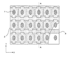
図2は、図1に示す画像表示装置の前面基板の内面図、図3は、図2の部分拡大図、図4は、図2,3中のA−A線に沿った断面図である。図2の右下部はメタルバックを剥ぎ取った状態(すなわち、発光部材と抵抗体が露出した状態)を示している。これらの図を参照して、前面基板4の構成について説明する。 2 is an internal view of the front substrate of the image display device shown in FIG. 1, FIG. 3 is a partially enlarged view of FIG. 2, and FIG. 4 is a cross-sectional view taken along line AA in FIGS. . The lower right part of FIG. 2 shows a state where the metal back is peeled off (that is, a state where the light emitting member and the resistor are exposed). The configuration of the front substrate 4 will be described with reference to these drawings.
前面基板4の内面には、赤(R)、緑(G)、青(B)に発光する多数の蛍光体からなる発光部材1が位置している。本実施形態の画像表示装置15は典型的な横長画面の画像表示装置であり、長軸方向をX方向(行方向)、短軸方向をY方向(列方向)としたときに、発光部材1は、X方向(行方向)、Y方向(列方向)に所定のピッチで行列状に配列されている。R,G,Bの蛍光体はX方向(行方向)に繰り返し配置されている。ここで、「所定のピッチ」は、製造上の誤差の範囲内で配列ピッチが変動する場合、あるいは設計上の理由により配列ピッチが変動する場合を含んでいる。発光部材1は、モノクローム、カラーによらず、沈殿法、スクリーン印刷法、ディスペンサ法等を用いて塗布形成することができる。
On the inner surface of the front substrate 4, a
発光部材1上には、アノード電極として機能するメタルバック層(電極)2が形成されている。メタルバック層2はX方向(行方向)及びY方向(列方向)に分断されている。すなわち、本実施形態では、一つのメタルバック層2が一つの発光部材1に対応し、各メタルバック層2が、対応する発光部材1を画像表示装置15の内面側から覆っている。メタルバック層2は、発光部材1の形成された、基板のほぼ全域に形成されている。メタルバック層2は、フォトエッチングによりパターニングする方法(フォトリソグラフィ法)を用いて形成することができる。または、所定の開口を有するメタルマスクを遮蔽部材として用いて真空蒸着する(マスク蒸着)方法によってもよい。
A metal back layer (electrode) 2 that functions as an anode electrode is formed on the
Y方向(列方向)に隣接するメタルバック層2の間(電極間)には、X方向(行方向)に連続して延びる抵抗体3が設けられている。抵抗体3は、図2の右下部分に示すように、Y方向(列方向)に一定幅のストライプ状の形状を有している。抵抗体3は、フォトリソグラフィ法、スクリーン印刷法、ディスペンサ法などによって形成できる。
Between the
図3を参照すると、メタルバック層2は、抵抗体3との接続部S1では抵抗体3を覆うように、すなわち抵抗体3に乗り上げるように形成されている。この結果、メタルバック層2は、X方向(行方向)に隣接するメタルバック層2同士、及びY方向(列方向)に隣接するメタルバック層2同士を電気的に接続している。図3には、行方向に隣接するメタルバック層2間に抵抗Rxが、列方向に隣接するメタルバック層2間に抵抗Ryが形成されることを模式的に示している。
Referring to FIG. 3, the
抵抗体3には、画像表示装置15に設けられた高圧電源(図示せず)からアノード電位が供給されている。従って、メタルバック層2は、抵抗体3を介してアノード電位に設定され、電子放出素子7から放出された電子ビームはアノード電圧により加速されて発光部材1に衝突し、画像が表示される。
The
メタルバック層2は、発光部材1を覆う部分S2におけるX方向(行方向)の幅Mxが抵抗体3との接続部S1におけるX方向(行方向)の幅Mx’よりも大きく形成されている。この結果、抵抗体との接続部S1におけるX方向(行方向)に隣接するメタルバック層2同士の行方向の離間距離Gx’は、発光部材を覆っている部分S2におけるX方向(行方向)に隣接するメタルバック層2同士の行方向の離間距離Gxよりも大きくなっている。この構成により、X方向(行方向)に隣接するメタルバック層2の先端部の離間距離を大きく確保でき、実質的に抵抗Rxを大きく設定することができる。換言すれば、あるメタルバックで放電が発生すると、隣接するメタルバックから抵抗体3を通して電子が流入するが、抵抗体3との接続部S1でメタルバック間の離間距離Gx’を大きく取ることで、抵抗体3の行方向の長さを確保することが容易となる。これによって、抵抗体3が隣接メタルバック2間の電位差に耐え易くなり、電極電圧をより高くすることが可能となるのである。従って、高輝度な画像表示が可能な前面基板を得ることができる。なお、メタルバック2間の離間距離Gxは放電電流仕様やプロセス上の都合などから適宜選択することができる。
The
また、列方向の発光部材の配列数は走査線の本数で限定されるため、実施形態によっては、メタルバック層2の列方向の離間距離Gyが行方向の離間距離Gxよりも大きくなることがある。この場合、抵抗Ryは大きくなるが、先端部を長くすることによって、すなわち接続部S1のY方向(列方向)の長さLを大きく取ることで、列方向に隣接するメタルバック層2の離間距離Gyを狭め、抵抗Ryを下げることができる。
In addition, since the number of light emitting members arranged in the column direction is limited by the number of scanning lines, the separation distance Gy in the column direction of the metal back
本実施形態では、隣接するメタルバック層2間の放電耐圧は、接続部S1におけるメタルバック間の離間距離Gx’で決定される。もし各メタルバック層2が矩形形状で、離間距離Gx’が発光部材1を覆っている部分S2における離間距離Gxと等しいならば、抵抗体3の高精度なパターン形成や抵抗体の塗り分けによって抵抗Rxを厳密に調整することが必要となる。しかし、離間距離Gx’は離間距離Gxより大きいため、抵抗体3の形成精度が抵抗Rxに与える影響が緩和され、抵抗体3の高精度なパターン形成は不要である。しかも、離間距離Gx’は発光部材1の配列ピッチとは無関係に決定できるため、調整の自由度も大きい。さらに、抵抗体3は、X方向(行方向)に一定の幅で延びる膜を形成するだけでよいため、製造プロセスも簡略化される。
In the present embodiment, the discharge breakdown voltage between the adjacent metal back layers 2 is determined by the separation distance Gx ′ between the metal backs in the connection portion S1. If each metal back
図2〜4に示した構成の前面基板を以下の工程により作製した。ガラス基板として、厚さ2.8mmのガラス基板(PD200、旭硝子社製)を用い、その上に遮光層としてNP−7803D(ノリタケ機材社製)を形成した。次に、R,G,Bの発光部材1を塗布焼成した後、ディスペンサ法で行方向に延びる長尺の抵抗体3を形成した。さらに、発光部材1の上にメタルバック層2をフォトリソグラフィ法により形成した。
A front substrate having the structure shown in FIGS. 2 to 4 was produced by the following steps. A glass substrate (PD200, manufactured by Asahi Glass Co., Ltd.) having a thickness of 2.8 mm was used as a glass substrate, and NP-7803D (manufactured by Noritake Equipment Co., Ltd.) was formed thereon as a light shielding layer. Next, R, G, and B
本実施例では、放電電流を1A以下に低減し、分断したメタルバック層2間に放電時に発生する電位差による2次的な放電を防ぐとともに、駆動時のアノード電位降下を250V以下に抑えて輝度低下を許容レベルにすることを目標とした。そのためには、Rx=367kΩ、Ry=250kΩで作成する必要がある。これらの値は、抵抗、容量、インダクタンス等が2次元的につながった等価回路モデルで事前に計算を行い算出した。求められる放電電流、隣接メタルバック間に発生する電位差、駆動時の輝度低下量に応じ、事前に等価回路モデルを立て計算を行うことにより、必要とされるRx、Ryの抵抗値を求めることが可能である。 In this embodiment, the discharge current is reduced to 1 A or less, secondary discharge due to the potential difference generated during the discharge between the divided metal back layers 2 is prevented, and the anode potential drop during driving is suppressed to 250 V or less. The goal was to bring the decline to an acceptable level. For this purpose, it is necessary to create the data with Rx = 367 kΩ and Ry = 250 kΩ. These values were calculated in advance using an equivalent circuit model in which resistance, capacitance, inductance, and the like were two-dimensionally connected. The required resistance values of Rx and Ry can be obtained by setting up an equivalent circuit model in advance according to the required discharge current, the potential difference generated between adjacent metal backs, and the amount of decrease in luminance during driving. Is possible.
本実施例では、メタルバック層2としてアルミニウム(Al)を用い、Rx=367kΩ、Ry=250kΩの抵抗値を実現した。具体的には、メタルバック層2の行方向の幅Mxを160μm、先端部分の行方向の幅(Mx’)を100μmで形成した(図3参照)。また、行方向に隣接するメタルバック層2の離間距離(Gx)を50μm、列方向に隣接するメタルバック層2の離間距離(Gy)を50μmで形成した。さらに、抵抗体3として体積抵抗が5Ω・mの抵抗材を用い、抵抗体3の列方向の幅を200μm、膜厚を10μmで形成した。行方向に隣接するメタルバック層2の先端部分の離間距離(Gx’)は110μmとなる。本実施例においては、メタルバック層2の幅が狭くなっている先端部分に抵抗体3を形成するため、Rx、Ryの抵抗値は隣接するメタルバック層2の先端部分の幅、間隔、長さにより規定される。
Rx=5Ω・m/10μm×110μm/(200−50)μm
Ry=5Ω・m/10μm×50μm/100μm
この前面基板を用いた画像表示装置を用い、内部の真空度を悪化させて耐放電テストを行ったところ、放電電流が1A以下に低減されていることが確認できた。行方向・列方向に分断したメタルバック層2間に発生する電位差による2次的な放電は発生しなかった。放電個所に点欠陥も発生せず、放電前の状態を維持することができた。また、画像形成装置の駆動時のアノード電位降下は250V以下になり、輝度低下も目視で確認する上では問題が無かった。
In this example, aluminum (Al) was used as the metal back
Rx = 5Ω · m / 10 μm × 110 μm / (200-50) μm
Ry = 5Ω · m / 10 μm × 50 μm / 100 μm
When an image display apparatus using this front substrate was used and a discharge resistance test was performed with the internal vacuum degree deteriorated, it was confirmed that the discharge current was reduced to 1 A or less. Secondary discharge due to a potential difference generated between the metal back layers 2 divided in the row direction and the column direction did not occur. No point defects occurred at the discharge location, and the state before discharge could be maintained. Further, the anode potential drop during driving of the image forming apparatus was 250 V or less, and there was no problem in visually confirming the brightness drop.
以上のように、量産に適したプロセスで製造可能な構成の前面基板、およびこれを用いた画像表示装置の耐放電性能を確認することができた。 As described above, it was possible to confirm the front substrate having a configuration that can be manufactured by a process suitable for mass production and the discharge resistance performance of an image display device using the front substrate.
1 発光部材
2 メタルバック層
3 抵抗体
S1 抵抗体との接続部
7 電子放出素子
15 画像表示装置
Gx 部分S2におけるメタルバック層同士の行方向の離間距離
Gx’ 接続部S1におけるメタルバック層同士の行方向の離間距離
DESCRIPTION OF
Claims (2)
前記基板上に行列状に位置する複数の発光部材と、
各々が少なくとも1つの前記発光部材を覆い、行列状に位置する複数の電極と、
列方向において隣接する前記電極間に位置し、行方向及び該列方向に隣接する電極同士を接続する行方向に延びるストライプ状の抵抗体と、
を有する前面基板において、
前記抵抗体との接続部における前記行方向に隣接する電極同士の行方向の離間距離は、前記発光部材を覆っている部分における前記行方向に隣接する電極同士の行方向の離間距離よりも大きいことを特徴とする前面基板。 A substrate,
A plurality of light emitting members positioned in a matrix on the substrate;
A plurality of electrodes, each covering at least one light emitting member and positioned in a matrix;
A striped resistor located between the electrodes adjacent in the column direction and extending in the row direction connecting the electrodes adjacent in the row direction and the column direction;
In a front substrate having
The separation distance in the row direction between the electrodes adjacent in the row direction in the connection portion with the resistor is larger than the separation distance in the row direction between the electrodes adjacent in the row direction in the portion covering the light emitting member. A front substrate characterized by that.
請求項1に記載の前面基板と、
を有し、前記電子放出素子から放出された電子によって前記発光部材が発光する、画像表示装置。 A back substrate having a plurality of electron-emitting devices;
The front substrate according to claim 1;
And the light emitting member emits light by electrons emitted from the electron emitting device.
Priority Applications (2)
| Application Number | Priority Date | Filing Date | Title |
|---|---|---|---|
| JP2008156665A JP2009301933A (en) | 2008-06-16 | 2008-06-16 | Front substrate and image display device using the same |
| US12/482,854 US8129892B2 (en) | 2008-06-16 | 2009-06-11 | Light emitter substrate and image displaying apparatus using the same |
Applications Claiming Priority (1)
| Application Number | Priority Date | Filing Date | Title |
|---|---|---|---|
| JP2008156665A JP2009301933A (en) | 2008-06-16 | 2008-06-16 | Front substrate and image display device using the same |
Publications (2)
| Publication Number | Publication Date |
|---|---|
| JP2009301933A true JP2009301933A (en) | 2009-12-24 |
| JP2009301933A5 JP2009301933A5 (en) | 2011-07-07 |
Family
ID=41414100
Family Applications (1)
| Application Number | Title | Priority Date | Filing Date |
|---|---|---|---|
| JP2008156665A Withdrawn JP2009301933A (en) | 2008-06-16 | 2008-06-16 | Front substrate and image display device using the same |
Country Status (2)
| Country | Link |
|---|---|
| US (1) | US8129892B2 (en) |
| JP (1) | JP2009301933A (en) |
Families Citing this family (2)
| Publication number | Priority date | Publication date | Assignee | Title |
|---|---|---|---|---|
| JP2009295532A (en) | 2008-06-09 | 2009-12-17 | Canon Inc | Light-emitting element substrate and image display device using the same |
| JP2010061999A (en) | 2008-09-04 | 2010-03-18 | Canon Inc | Emitter substrate and image display apparatus using the same |
Family Cites Families (5)
| Publication number | Priority date | Publication date | Assignee | Title |
|---|---|---|---|---|
| JP4027386B2 (en) * | 2004-11-18 | 2007-12-26 | キヤノン株式会社 | Luminescent screen structure and image forming apparatus |
| JP4551755B2 (en) | 2004-12-24 | 2010-09-29 | キヤノン株式会社 | Image display device |
| JP2009176424A (en) | 2008-01-21 | 2009-08-06 | Canon Inc | Image display apparatus |
| JP2009295532A (en) | 2008-06-09 | 2009-12-17 | Canon Inc | Light-emitting element substrate and image display device using the same |
| JP2009301932A (en) | 2008-06-16 | 2009-12-24 | Canon Inc | Front substrate and image display device using the same |
-
2008
- 2008-06-16 JP JP2008156665A patent/JP2009301933A/en not_active Withdrawn
-
2009
- 2009-06-11 US US12/482,854 patent/US8129892B2/en not_active Expired - Fee Related
Also Published As
| Publication number | Publication date |
|---|---|
| US20090309480A1 (en) | 2009-12-17 |
| US8129892B2 (en) | 2012-03-06 |
Similar Documents
| Publication | Publication Date | Title |
|---|---|---|
| JP5317658B2 (en) | Light emitting substrate and display device using the same | |
| JP2006120622A (en) | Luminescent screen structure and image forming apparatus | |
| JP4115403B2 (en) | Luminescent substrate and image display device | |
| JP2008159449A (en) | Display device | |
| KR100742096B1 (en) | Image display | |
| US8072133B2 (en) | Light emitter substrate and image displaying apparatus using the same | |
| JP2009301932A (en) | Front substrate and image display device using the same | |
| JP2010015870A (en) | Image display device | |
| JP2009301933A (en) | Front substrate and image display device using the same | |
| WO2005124814A1 (en) | Planar display device | |
| JP2006185701A (en) | Image display device | |
| JP2005268109A (en) | Light emitting body substrate and image display device using it | |
| EP1732143A1 (en) | Image display | |
| EP1760757A1 (en) | Image display device and method for manufacturing the same | |
| JP2005294157A (en) | Image display device | |
| US8044568B2 (en) | Light emitter substrate with different gaps between metal backs and image displaying apparatus using the same | |
| JP2006120422A (en) | Display and manufacturing method thereof | |
| US20100148655A1 (en) | Light-emitting substrate and image display apparatus | |
| EP1734557A1 (en) | Image display apparatus | |
| US20100148670A1 (en) | Electron source substrate and image display apparatus | |
| JP2006066201A (en) | Image display device and its manufacturing method | |
| JP2006092963A (en) | Image display device | |
| JP2005259517A (en) | Display device | |
| JP2012221896A (en) | Image display device | |
| JP2006107765A (en) | Image display device and its manufacturing method |
Legal Events
| Date | Code | Title | Description |
|---|---|---|---|
| A521 | Written amendment |
Free format text: JAPANESE INTERMEDIATE CODE: A523 Effective date: 20110523 |
|
| A621 | Written request for application examination |
Free format text: JAPANESE INTERMEDIATE CODE: A621 Effective date: 20110523 |
|
| A761 | Written withdrawal of application |
Free format text: JAPANESE INTERMEDIATE CODE: A761 Effective date: 20111212 |