JP2009295904A - Surface-emitting laser - Google Patents
Surface-emitting laser Download PDFInfo
- Publication number
- JP2009295904A JP2009295904A JP2008150284A JP2008150284A JP2009295904A JP 2009295904 A JP2009295904 A JP 2009295904A JP 2008150284 A JP2008150284 A JP 2008150284A JP 2008150284 A JP2008150284 A JP 2008150284A JP 2009295904 A JP2009295904 A JP 2009295904A
- Authority
- JP
- Japan
- Prior art keywords
- refractive index
- periodic structure
- layer
- photonic crystal
- emitting laser
- Prior art date
- Legal status (The legal status is an assumption and is not a legal conclusion. Google has not performed a legal analysis and makes no representation as to the accuracy of the status listed.)
- Granted
Links
Images


Abstract
Description
本発明は、面発光レーザに関するものである。 The present invention relates to a surface emitting laser.
近年、面発光レーザが盛んに研究されている。面発光レーザは、集積化アレイ化が容易、外部光学系との結合効率が優れているなどの利点があり、通信、電子写真、センシングなどの分野に応用が期待されている。
特に、赤外線短距離通信などの通信分野においては、すでに実用化されている。
In recent years, surface emitting lasers have been actively studied. A surface emitting laser has advantages such as easy integration into an array and excellent coupling efficiency with an external optical system, and is expected to be applied in fields such as communication, electrophotography, and sensing.
In particular, it has already been put into practical use in the communication field such as infrared short-range communication.
面発光レーザにはいくつかの種類が存在するが、その中の一つとして、基板に平行な方向に光を共振させ、発振したレーザ光を、基板に垂直方向に回折させて取り出すことで面発光機能を持たせるレーザ素子がある。
これは、レーザの形式としては、現在世の中で広く用いられているDFB(Distributed Feedback)レーザの一形態である。
There are several types of surface emitting lasers. One of them is to resonate light in a direction parallel to the substrate, and oscillate the laser beam oscillated in a direction perpendicular to the substrate. There is a laser element that has a light emitting function.
This is a form of a DFB (Distributed Feedback) laser that is widely used in the world as a type of laser.
特許文献1には、このような面発光レーザとして、2次元フォトニック結晶の回折効果を用いたレーザ素子(半導体発光デバイス)およびその製造法が開示されている。
このレーザ素子においては、半導体レーザの活性層の近傍にフォトニック結晶を導入し、活性層内部で発光した光をフォトニック結晶の2次回折効果により面内方向で発振させる。
そして、発振したレーザ光を、同一フォトニック結晶の1次回折により、面垂直方向に取り出す。
In this laser element, a photonic crystal is introduced in the vicinity of the active layer of the semiconductor laser, and light emitted inside the active layer is oscillated in the in-plane direction by the second-order diffraction effect of the photonic crystal.
The oscillated laser light is extracted in the direction perpendicular to the plane by the first-order diffraction of the same photonic crystal.
しかしながら、上記した従来例のような面発光レーザにおいては、低閾値化の観点から、更なる性能向上が望まれている。
本発明は、上記課題に鑑み、従来例よりも低閾値で動作することが可能となる面発光レーザを提供することを目的とする。
However, in the surface emitting laser as in the conventional example described above, further performance improvement is desired from the viewpoint of lowering the threshold.
In view of the above problems, an object of the present invention is to provide a surface emitting laser that can operate at a lower threshold than the conventional example.
本発明は、つぎのように構成した面発光レーザを提供するものである。
本発明の面発光レーザは、活性層を備えた導波路層と、前記活性層からの光と結合する位置に設けられた屈折率周期構造と、を有する面発光レーザであって、
前記屈折率周期構造が、前記活性層側に設けられている低屈折率媒質と高屈折率媒質とからなる第1の屈折率周期構造層と、該第1の屈折率周期構造層上に積層された低屈折率媒質と高屈折率媒質とからなる第2の屈折率周期構造層とを備え、
前記第2の屈折率周期構造層における前記低屈折率媒質の体積分率が、前記第1の屈折率周期構造層における前記低屈折率媒質よりも大きい体積分率を有していることを特徴とする。
また、本発明の面発光レーザは、前記第1の屈折率周期構造層における屈折率周期構造が2次元周期構造であり、
前記第2の屈折率周期構造層における屈折率周期構造が1次元周期構造であることを特徴とする。
また、本発明の面発光レーザは、前記第1の屈折率周期構造層における屈折率周期構造を構成するパターンが正方格子状であり、
前記第2の屈折率周期構造層における屈折率周期構造を構成するパターンがストライプ状であることを特徴とする。
また、本発明の面発光レーザは、前記第1の屈折率周期構造層を構成する低屈折率媒質としての気体媒質の体積分率が16%以上であり、
前記第2の屈折率周期構造層を構成する低屈折率媒質としての気体媒質の体積分率が52%より大きく97%以下であることを特徴とする。
また、本発明の面発光レーザは、前記第2の屈折率周期構造層に隣接して、電極が形成されていることを特徴とする。
また、本発明の面発光レーザは、前記電極が、前記第2の屈折率周期構造層における前記高屈折率媒質の全部と、前記第2の屈折率周期構造層における前記低屈折率媒質の一部に隣接して、形成されていることを特徴とする。
また、本発明の面発光レーザは、前記電極が、前記第2の屈折率周期構造層における前記高屈折率媒質の上に形成されており、
前記第2の屈折率周期構造層における前記高屈折率媒質のパターンと、前記電極のパターンとが、同一のパターンであることを特徴とする。
また、本発明の面発光レーザは、前記第1の屈折率周期構造層における前記低屈折率媒質が、環状形状であることを特徴とする。
また、本発明の面発光レーザは、前記第2の屈折率周期構造層における周期構造の周期が、不規則にずれて構成されていることを特徴とする。
The present invention provides a surface emitting laser configured as follows.
The surface-emitting laser of the present invention is a surface-emitting laser having a waveguide layer including an active layer and a refractive index periodic structure provided at a position where it is coupled with light from the active layer,
The refractive index periodic structure is laminated on the first refractive index periodic structure layer, a first refractive index periodic structure layer comprising a low refractive index medium and a high refractive index medium provided on the active layer side A second refractive index periodic structure layer comprising a low refractive index medium and a high refractive index medium,
The volume fraction of the low refractive index medium in the second refractive index periodic structure layer is larger than the volume fraction of the low refractive index medium in the first refractive index periodic structure layer. And
In the surface emitting laser of the present invention, the refractive index periodic structure in the first refractive index periodic structure layer is a two-dimensional periodic structure,
The refractive index periodic structure in the second refractive index periodic structure layer is a one-dimensional periodic structure.
Further, in the surface emitting laser of the present invention, the pattern constituting the refractive index periodic structure in the first refractive index periodic structure layer is a square lattice shape,
The pattern constituting the refractive index periodic structure in the second refractive index periodic structure layer is striped.
In the surface emitting laser of the present invention, the volume fraction of the gas medium as the low refractive index medium constituting the first refractive index periodic structure layer is 16% or more,
A volume fraction of a gas medium as a low refractive index medium constituting the second refractive index periodic structure layer is more than 52% and not more than 97%.
The surface emitting laser of the present invention is characterized in that an electrode is formed adjacent to the second refractive index periodic structure layer.
In the surface emitting laser according to the present invention, the electrode may include one of the high refractive index medium in the second refractive index periodic structure layer and one of the low refractive index media in the second refractive index periodic structure layer. It is formed adjacent to the part.
In the surface emitting laser of the present invention, the electrode is formed on the high refractive index medium in the second refractive index periodic structure layer,
The pattern of the high refractive index medium and the pattern of the electrode in the second refractive index periodic structure layer are the same pattern.
In the surface emitting laser of the present invention, the low refractive index medium in the first refractive index periodic structure layer has an annular shape.
The surface emitting laser according to the present invention is characterized in that the period of the periodic structure in the second refractive index periodic structure layer is irregularly shifted.
本発明によれば、従来例よりも低閾値で動作することが可能となる面発光レーザを実現することができる。 According to the present invention, it is possible to realize a surface emitting laser that can operate at a lower threshold than the conventional example.
本発明の実施形態における活性層を備えた導波路層と、前記活性層からの光と結合する位置に設けられた屈折率周期構造と、を有する面発光レーザについて、図を用いて説明する。
図1に、本実施形態の面発光レーザにおける素子構造の全体構成を説明する断面図を示す。
図1において、101は基板、102はクラッド層、103は下部導波路層、104は活性層、105は上部導波路層、106は導波路層である。
107は第1の屈折率周期構造層である下部屈折率周期構造層、108は第2の屈折率周期構造層である上部屈折率周期構造層、109は屈折率周期構造層である。
110は下層高屈折率媒質、111は下層低屈折率媒質、112は上層高屈折率媒質、113は上層低屈折率媒質である。
114は下部電極、115は上部電極である。
A surface-emitting laser having a waveguide layer including an active layer and a refractive index periodic structure provided at a position where it couples with light from the active layer according to an embodiment of the present invention will be described with reference to the drawings.
FIG. 1 is a cross-sectional view illustrating the overall configuration of the element structure of the surface emitting laser according to the present embodiment.
In FIG. 1, 101 is a substrate, 102 is a cladding layer, 103 is a lower waveguide layer, 104 is an active layer, 105 is an upper waveguide layer, and 106 is a waveguide layer.
Reference numeral 107 denotes a lower refractive index periodic structure layer which is a first refractive index periodic structure layer, 108 denotes an upper refractive index periodic structure layer which is a second refractive index periodic structure layer, and 109 denotes a refractive index periodic structure layer.
Reference numeral 110 denotes a lower layer high refractive index medium, 111 denotes a lower layer low refractive index medium, 112 denotes an upper layer high refractive index medium, and 113 denotes an upper layer low refractive index medium.
Reference numeral 114 denotes a lower electrode, and 115 denotes an upper electrode.
本実施形態の面発光レーザは、基板101の上にクラッド層102が設けられ、更にその上に、下部導波路層103と上部導波路層105との間に活性層104を挟持して構成された導波路層106が設けられている。
この導波路層106上には屈折率周期構造が設けられており、この屈折率周期構造は活性層側に設けられている第1の屈折率周期構造層と該第1の屈折率周期構造層上に積層された第2の屈折率周期構造層とによって構成されている。
具体的には、上部導波路層105の上に、高屈折率媒質と低屈折率媒質よりなる下部屈折率周期構造層(第1の屈折率周期構造層)107と、上部屈折率周期構造層(第2の屈折率周期構造層)108によって構成された屈折率周期構造層109が設けられている。
さらに、上記の下部屈折率周期構造層107は下層高屈折率媒質110および下層低屈折率媒質111により形成され、上部屈折率周期構造層108は上層高屈折率媒質112および上層低屈折率媒質113により形成されている。
下部電極114と上部電極115はそれぞれ基板101の裏面、上部屈折率周期構造層108の上層に設けられている。
The surface emitting laser of this embodiment is configured by providing a clad layer 102 on a substrate 101 and further sandwiching an active layer 104 between a lower waveguide layer 103 and an upper waveguide layer 105 thereon. A waveguide layer 106 is provided.
A refractive index periodic structure is provided on the waveguide layer 106. The refractive index periodic structure includes a first refractive index periodic structure layer and a first refractive index periodic structure layer provided on the active layer side. It is comprised by the 2nd refractive index periodic structure layer laminated | stacked on the top.
Specifically, on the upper waveguide layer 105, a lower refractive index periodic structure layer (first refractive index periodic structure layer) 107 composed of a high refractive index medium and a low refractive index medium, and an upper refractive index periodic structure layer. A refractive index periodic structure layer 109 constituted by (second refractive index periodic structure layer) 108 is provided.
Further, the lower refractive index periodic structure layer 107 is formed of a lower high refractive index medium 110 and a lower low refractive index medium 111, and the upper refractive index periodic structure layer 108 is composed of an upper high refractive index medium 112 and an upper low refractive index medium 113. It is formed by.
The lower electrode 114 and the upper electrode 115 are provided on the back surface of the substrate 101 and on the upper layer of the upper refractive index periodic structure layer 108, respectively.
つぎに、本実施の形態における、屈折率周期構造層109の機能について説明する。
屈折率周期構造層109は高屈折率媒質と低屈折率媒質が交互に周期構造を形成している。
このような屈折率周期構造層は、例えば、フォトニック結晶などを用いて構成することができる。
本実施形態における面発光レーザにおいては、屈折率周期構造層109は、活性層からの発光を面内方向にフィードバックし、さらに発振した光を上方に回折することにより面発光する。
Next, the function of the refractive index periodic structure layer 109 in this embodiment will be described.
In the refractive index periodic structure layer 109, a high refractive index medium and a low refractive index medium alternately form a periodic structure.
Such a refractive index periodic structure layer can be configured using, for example, a photonic crystal.
In the surface emitting laser according to the present embodiment, the refractive index periodic structure layer 109 feeds back light emitted from the active layer in the in-plane direction, and further emits light by diffracting the oscillated light upward.
本実施形態の面発光レーザにおける屈折率周期構造層109では、上部屈折率周期構造層108における低屈折率媒質の体積分率が、下部屈折率周期構造層107における低屈折率媒質よりも大きい体積分率を有する構成とされている。
このような構成を備えた屈折率周期構造層109では、レーザのフィードバック機能をメインに持つのは下部屈折率周期構造層107であり、上部屈折率周期構造層108は、低屈折率媒質の割合が大きいため、光を閉じ込めるための閉じ込め層の機能を有している。
このように上部と下部の屈折率周期構造層の機能を分離することで、下部屈折率周期構造層によるフィードバック効果を高めながら、上部屈折率周期構造層による閉じ込めで光を電極に吸収させないようにすることができる。
これにより、素子の閾値を下げることが可能となる。
さらに、上部屈折率周期構造層を100〜200nm程度に薄くすることが可能なため、貼りあわせなどを用いず素子を一括で作成することが可能となる。
In the refractive index periodic structure layer 109 in the surface emitting laser of the present embodiment, the volume fraction of the low refractive index medium in the upper refractive index periodic structure layer 108 is larger than that of the low refractive index medium in the lower refractive index periodic structure layer 107. It is set as the structure which has a fraction.
In the refractive index periodic structure layer 109 having such a configuration, the lower refractive index periodic structure layer 107 mainly has a laser feedback function, and the upper refractive index periodic structure layer 108 is a ratio of a low refractive index medium. Therefore, it has a function of a confinement layer for confining light.
By separating the functions of the upper and lower refractive index periodic structure layers in this way, the feedback effect by the lower refractive index periodic structure layer is enhanced, and confinement by the upper refractive index periodic structure layer prevents light from being absorbed by the electrode. can do.
Thereby, the threshold value of the element can be lowered.
Furthermore, since the upper refractive index periodic structure layer can be thinned to about 100 to 200 nm, it is possible to collectively form elements without using bonding or the like.
図9に、本実施形態の面発光レーザにおける上部屈折率周期構造層の空孔部の体積分率を下部屈折率周期構造層に比べて等しくした時と大きくした時とで、共振光の電極による吸収率を比較するグラフを示す。
図9では、格子定数a、屈折率周期構造の厚さを固定し、横軸で上部屈折率周期構造層の半径を変化させ、共振光の上部電極115による吸収率を見たものである。
上部屈折率周期構造層の低屈折率媒質の体積分率が下層と同じときと、下部屈折率周期構造層よりも大きいときとの両方の結果を示すが、この図9によれば上部屈折率周期構造層の体積分率が大きい時の方が吸収率が小さくなることが分かる。
FIG. 9 shows the resonant light electrodes when the volume fraction of the holes of the upper refractive index periodic structure layer in the surface emitting laser of this embodiment is made equal to and larger than that of the lower refractive index periodic structure layer. The graph which compares the absorption rate by is shown.
In FIG. 9, the lattice constant a and the thickness of the refractive index periodic structure are fixed, the radius of the upper refractive index periodic structure layer is changed on the horizontal axis, and the absorption rate of the resonant light by the upper electrode 115 is observed.
The results of both the case where the volume fraction of the low refractive index medium of the upper refractive index periodic structure layer is the same as that of the lower layer and the case where the volume fraction of the lower refractive index periodic structure layer is larger than that of the lower refractive index periodic structure layer are shown. It can be seen that the absorption rate is smaller when the volume fraction of the periodic structure layer is larger.
屈折率周期構造層109は、屈折率のコントラストが大きい方が好ましいため、例えば、高屈折率の半導体材料に空孔を設けた構成などが好ましい。
このとき下部屈折率周期構造層107は、フォトニック結晶に共振光を大きく染み出させフィードバック効果を高めるため、空孔の大きさはある程度小さい方がよい。しかしながら、あまりに小さくし過ぎると、作製も困難になり、フィードバック効果も下がってしまうことになるため、そこには一定の好ましい範囲がある。
具体的には、周期構造の周期をaとした時、半径rでおよそ0.13a〜0.28aの範囲内(低屈折率媒質の体積分率にして5%〜25%程度)とすることが好ましい。
また、低屈折率媒質が導電性の固体の場合は電流注入の経路が広くなるため、電流注入の観点からは好ましい。これらは後述するように、電極の構造にも依存する。
Since the refractive index periodic structure layer 109 preferably has a higher refractive index contrast, for example, a structure in which holes are provided in a high refractive index semiconductor material is preferable.
At this time, since the lower refractive index periodic structure layer 107 oozes resonance light into the photonic crystal to enhance the feedback effect, the size of the holes is preferably small to some extent. However, if it is too small, it will be difficult to produce and the feedback effect will be reduced, so there is a certain preferred range there.
Specifically, when the period of the periodic structure is a, the radius r is within the range of about 0.13a to 0.28a (the volume fraction of the low refractive index medium is about 5% to 25%). Is preferred.
Further, when the low refractive index medium is a conductive solid, the current injection path is wide, which is preferable from the viewpoint of current injection. As will be described later, these also depend on the structure of the electrode.
上部屈折率周期構造層108においては、本発明の効果を得るためには、少なくとも低屈折率媒質の体積分率が、下部屈折率周期構造層107よりも大きいことが必要がある。
また、本実施形態においては、屈折率周期構造層の説明において、便宜上、周期構造の周期が一定のものについて説明したが、必ずしも周期構造の周期が一定である必要はない。
例えば、上部屈折率周期構造層108における周期構造の周期がランダム(不規則)にずれて構成されていてもよく、このような構造とした場合にはプロセスの制約などを緩和することができる点において好ましい。
In the upper refractive index periodic structure layer 108, in order to obtain the effect of the present invention, at least the volume fraction of the low refractive index medium needs to be larger than that of the lower refractive index periodic structure layer 107.
In the present embodiment, in the description of the refractive index periodic structure layer, the periodic structure has a constant period for convenience. However, the period of the periodic structure does not necessarily have to be constant.
For example, the period of the periodic structure in the upper refractive index periodic structure layer 108 may be configured to be randomly (irregular) shifted. With such a structure, process restrictions and the like can be relaxed. Is preferable.
また、下部、上部屈折率周期構造の周期構造の配列は、対称性、周期などで必ずしも同じでなくともよい。
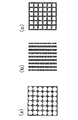
例えば、下部屈折率周期構造層(第1の屈折率周期構造層)における屈折率周期構造を、図2(a)、(c)のように、該屈折率周期構造を構成するパターンを正方格子状に配列した2次元周期構造とする。
一方、上部屈折率周期構造層(第2の屈折率周期構造層)における屈折率周期構造を、図2(b)のように、該屈折率周期構造を構成するパターンをストライプ状として1次元周期構造とすることも可能である。
これらの構成例については、後の実施例2で説明する。
また、格子点およびストライプラインの形状もそれぞれ違っていてもよい。
例えば、下部屈折率周期構造、上部屈折率周期構造ともに2次元の正方格子とし、下部屈折率周期構造の格子点形状を図2(a)のような円形に、上部周期構造の格子点形状を図2(c)のような正方形とすることも可能である。
Further, the arrangement of the periodic structures of the lower and upper refractive index periodic structures may not necessarily be the same due to symmetry, period, and the like.
For example, the refractive index periodic structure in the lower refractive index periodic structure layer (first refractive index periodic structure layer) is represented by a square lattice as shown in FIGS. 2 (a) and 2 (c). A two-dimensional periodic structure arranged in a shape.
On the other hand, the refractive index periodic structure in the upper refractive index periodic structure layer (second refractive index periodic structure layer) is changed to a one-dimensional period with the pattern constituting the refractive index periodic structure as stripes as shown in FIG. A structure is also possible.
Examples of these configurations will be described later in Example 2.
Further, the lattice points and the stripe lines may have different shapes.
For example, both the lower refractive index periodic structure and the upper refractive index periodic structure are two-dimensional square lattices, the lattice point shape of the lower refractive index periodic structure is circular as shown in FIG. It is also possible to use a square as shown in FIG.
さらに、本実施形態においては、2次元の屈折率周期構造は正方格子のものについて説明したが、これらに限られるものではない。
例えば、長方格子、三角格子、円対称格子、準結晶などの対称性を用いることも可能である。格子点形状も円形、正方形のみ紹介したが、その他、楕円形、三角形、長方形、環状形状、十字形状など、様々な形状の格子点を用いることができる。
なお、格子点が環状形状の場合については、実施例3にて説明する。
また、上層、下層ともに1次元の周期構造を用いることも可能である。
Furthermore, in the present embodiment, the two-dimensional refractive index periodic structure has been described as a square lattice, but is not limited thereto.
For example, symmetry such as a rectangular lattice, a triangular lattice, a circularly symmetric lattice, and a quasicrystal can be used. Although only the circular and square grid shapes have been introduced, various other grid points such as an ellipse, a triangle, a rectangle, an annular shape, and a cross shape can be used.
The case where the lattice points are annular will be described in Example 3.
It is also possible to use a one-dimensional periodic structure for both the upper layer and the lower layer.
屈折率周期構造層109を構成するフォトニック結晶の材料としては、光損失の少ない半導体材料や、酸化物透明導電媒質などを用いることができる。
本実施形態においては、周期構造を通して電流を注入するため、材料は導電性を有する必要がある。
半導体材料としては、キャリアドープされたGaAs、AlGaAs、InP、GaAsInP、AlGaInP、GaN、InGaN、AlGaN、AlN、InNなどのIII−V族化合物半導体およびそれらの任意の混晶などを用いることができる。
また、ZnSe、CdS、ZnOなどのII−VI族化合物半導体およびそれらの任意の混晶、Si、SiGeなどのIV族半導体およびそれらの任意の混晶などを用いることができる。さらに、各種の有機半導体なども使用可能である。
酸化物透明導電媒質としてはITO(Indium Tin Oxaide)SnO2、In2O3などがある。
上部および下部の屈折率周期構造層における低屈折率媒質は固体でも空気でも良いが、固体の場合は電流注入の経路が広くなるため好ましい。これらは後述するように、電極の構造にも依存する。
As a material of the photonic crystal constituting the refractive index periodic structure layer 109, a semiconductor material with little light loss, an oxide transparent conductive medium, or the like can be used.
In the present embodiment, since current is injected through the periodic structure, the material needs to have conductivity.
As the semiconductor material, carrier-doped GaAs, AlGaAs, InP, GaAsInP, AlGaInP, GaN, InGaN, AlGaN, AlN, InN, and other III-V group compound semiconductors and arbitrary mixed crystals thereof can be used.
Moreover, II-VI group compound semiconductors, such as ZnSe, CdS, ZnO, and those arbitrary mixed crystals, IV group semiconductors, such as Si and SiGe, and those arbitrary mixed crystals, etc. can be used. Furthermore, various organic semiconductors can be used.
Examples of the oxide transparent conductive medium include ITO (Indium Tin Oxide) SnO 2 and In 2 O 3 .
The low refractive index medium in the upper and lower refractive index periodic structure layers may be either solid or air, but a solid is preferable because the current injection path becomes wider. As will be described later, these also depend on the structure of the electrode.
つぎに、本実施形態における活性層、導波路層、クラッド層、等について説明する。
活性層104には量子井戸構造、ひずみ量子井戸構造、量子ドット構造などを用いることができる。
また、クラッド層102は、導波路層106に対して屈折率が低くなっていることが必要である。
また、本実施形態には記載していないが、クラッド層102、導波路層106のいずれかの層に、水蒸気酸化やイオン注入による電流狭窄層や、キャリアの漏れを抑えるキャリアブロック層を設けることも可能である。
活性層、クラッド層に用いることのできる材料は半導体であり、上述したようなフォトニック結晶に用いることのできる半導体材料は全て使用することができる。
クラッド層102および導波路層106の一部は、nまたはpのキャリアがドープされている。
Next, an active layer, a waveguide layer, a cladding layer, and the like in this embodiment will be described.
For the active layer 104, a quantum well structure, a strained quantum well structure, a quantum dot structure, or the like can be used.
Further, the cladding layer 102 needs to have a lower refractive index than the waveguide layer 106.
Although not described in this embodiment, a current confinement layer by steam oxidation or ion implantation or a carrier block layer for suppressing carrier leakage is provided in any one of the cladding layer 102 and the waveguide layer 106. Is also possible.
The material that can be used for the active layer and the clad layer is a semiconductor, and all the semiconductor materials that can be used for the photonic crystal as described above can be used.
A part of the cladding layer 102 and the waveguide layer 106 is doped with n or p carriers.
つぎに、本実施形態における電流注入方法について説明する。
本実施形態における面発光レーザは、下部電極114、上部電極115を、p電極またはn電極とし(逆でも可)、電極からの電流注入により駆動させることができる。
電極を構成する材料としては、従来の半導体レーザプロセスなどで用いられている材料をはじめとし、あらゆる金属材料を用いることが可能である。
特に、半導体材料に関しては、従来の半導体レーザプロセスにおいて、半導体材料に応じて使用できる電極材料がほぼ決まっており、電極を形成する技術はほとんど確立されているため、それに従えばよい。
例えば、GaAsのn電極には、Au−Ge−Ni、Au−Ge−Pt、p電極にはAg−Zn、Au−Znなどの材料が用いられる。
また、金属以外にも、ITO、SnO2、InO2などの、導電性を有する透明酸化物材料などを電極に用いることも可能である。
Next, the current injection method in this embodiment will be described.
In the surface emitting laser according to the present embodiment, the lower electrode 114 and the upper electrode 115 can be p-electrodes or n-electrodes (or vice versa) and can be driven by current injection from the electrodes.
As a material constituting the electrode, any metal material can be used including a material used in a conventional semiconductor laser process or the like.
In particular, with respect to semiconductor materials, electrode materials that can be used according to semiconductor materials are almost determined in conventional semiconductor laser processes, and almost all techniques for forming electrodes have been established.
For example, materials such as Au—Ge—Ni and Au—Ge—Pt are used for the n electrode of GaAs, and Ag—Zn and Au—Zn are used for the p electrode.
In addition to metals, conductive transparent oxide materials such as ITO, SnO 2 and InO 2 can also be used for the electrodes.
つぎに、本実施形態における電極パターンと光取り出し方法について説明する。
本実施形態においては、上部屈折率周期構造層に隣接して形成された電極が、上部屈折率周期構造層における前記高屈折率媒質のパターンと同一のパターンにパターニングされているが、このような構成に限定されるものではない。
例えば、電極方向に光を取り出す構成になっているが、パターニングしない平板状の電極を設けることも可能である。
このような電極においては、特に上部屈折率周期構造層の低屈折率媒質が導電性のある固体媒質で構成されているような場合、電極の接触面積が広くなることで電気抵抗が低くなり好ましい。
但し、このような電極の場合、吸収により出射光を電極方向から取り出すことは出来ないため、基板方向から取り出すことになる。このとき基板は出射光を吸収しないことが必要である。
また、出射光を吸収する場合も、出射部の基板を裏抜きするなどして吸収を減らすことで、裏面より出射光を取り出すことができる。
さらに、この電極とフォトニック結晶層との距離を調整することで、電極方向に出射する光を適当な位相で返すようにすることで、さらに閾値を下げることもできる。
Next, an electrode pattern and a light extraction method in this embodiment will be described.
In the present embodiment, the electrode formed adjacent to the upper refractive index periodic structure layer is patterned in the same pattern as the pattern of the high refractive index medium in the upper refractive index periodic structure layer. The configuration is not limited.
For example, although it is configured to extract light in the electrode direction, it is possible to provide a flat electrode that is not patterned.
In such an electrode, in particular, when the low refractive index medium of the upper refractive index periodic structure layer is composed of a conductive solid medium, it is preferable because the contact area of the electrode is widened to reduce the electric resistance. .
However, in the case of such an electrode, emitted light cannot be extracted from the electrode direction due to absorption, and thus is extracted from the substrate direction. At this time, it is necessary that the substrate does not absorb the emitted light.
Further, also when the emitted light is absorbed, the emitted light can be extracted from the back surface by reducing the absorption by, for example, removing the substrate of the emitting portion.
Further, by adjusting the distance between the electrode and the photonic crystal layer, the light emitted in the electrode direction is returned in an appropriate phase, so that the threshold can be further lowered.
以下に、本発明の実施例について説明する。
[実施例1]
実施例1においては、本発明を適用した面発光レーザの構成例について説明する。
図3に、本実施例における面発光レーザの構成例を説明する模式図を示す。
図3(a)は面発光レーザ全体の斜視図、図3(b)は図3(a)に示す面発光レーザをa−a’に沿ってz軸方向に切断した断面における模式的断面図、図3(c)は図3(a)に示す面発光レーザをz方向よりみた模式的平面図である。図3において、301は基板、302はクラッド層、303は下部導波路層、304は活性層、305は上部導波路層である。
307は下部フォトニック結晶層、308は上部フォトニック結晶層、309はフォトニック結晶層、311は下層フォトニック結晶層空孔、313は上層フォトニック結晶層空孔、314はn電極、315はp電極である。
Examples of the present invention will be described below.
[Example 1]
In Example 1, a configuration example of a surface emitting laser to which the present invention is applied will be described.
FIG. 3 is a schematic diagram illustrating a configuration example of the surface emitting laser in the present embodiment.
3A is a perspective view of the entire surface emitting laser, and FIG. 3B is a schematic sectional view of the surface emitting laser shown in FIG. 3A taken along the line aa ′ in the z-axis direction. FIG. 3C is a schematic plan view of the surface emitting laser shown in FIG. In FIG. 3, 301 is a substrate, 302 is a cladding layer, 303 is a lower waveguide layer, 304 is an active layer, and 305 is an upper waveguide layer.
307 is a lower photonic crystal layer, 308 is an upper photonic crystal layer, 309 is a photonic crystal layer, 311 is a lower photonic crystal layer hole, 313 is an upper photonic crystal layer hole, 314 is an n electrode, 315 is p electrode.
本実施例における面発光レーザは、図3(a)に示すように、基板301上に、まず厚さ1μmのクラッド層302が積層されている。
さらに、下部導波路層303が厚さ100μm、活性層304が厚さ24nm、上部導波路層305が厚さ100nmで積層されている。
さらに、上部導波路層305の上に、フォトニック結晶層309を厚さ200nmの順番に積層した構造を有している。
基板裏面301、フォトニック結晶層309の上層にはそれぞれn電極314、p電極315が設けられている。p電極の方は上部フォトニック結晶層と同様にパターニングされている。
In the surface emitting laser of this embodiment, as shown in FIG. 3A, a clad layer 302 having a thickness of 1 μm is first laminated on a substrate 301.
Further, the lower waveguide layer 303 is laminated with a thickness of 100 μm, the active layer 304 is laminated with a thickness of 24 nm, and the upper waveguide layer 305 is laminated with a thickness of 100 nm.
Further, the photonic crystal layer 309 is stacked on the upper waveguide layer 305 in order of 200 nm in thickness.
An n-electrode 314 and a p-electrode 315 are provided on the substrate back surface 301 and the photonic crystal layer 309, respectively. The p electrode is patterned in the same manner as the upper photonic crystal layer.
図3(b)に示すように、フォトニック結晶層309は下部フォトニック結晶層307、上部フォトニック結晶層308の2層に分かれており、フォトニック結晶の空孔部の体積分率について、上層空孔313が下層空孔311よりも大きくなっている。
フォトニック結晶は個体媒質に空孔を導入した構成であり、上部下部とも格子形状は円形、配置は正方格子状となっている。
図3(c)の平面図には、上部、下部結晶層の空孔部が図示されており、上部層の方が空孔径が大きくなっている。
なお、図3(c)における空孔数は、図3(a)と異なっているが、これも図示の際の便宜上の理由のみで、実際の空孔数は両者等しくなっている。
As shown in FIG. 3B, the photonic crystal layer 309 is divided into two layers, a lower photonic crystal layer 307 and an upper photonic crystal layer 308. Regarding the volume fraction of the hole portion of the photonic crystal, The upper layer hole 313 is larger than the lower layer hole 311.
The photonic crystal has a structure in which holes are introduced into a solid medium, and the upper and lower portions have a circular lattice shape and a square lattice arrangement.
In the plan view of FIG. 3C, the hole portions of the upper and lower crystal layers are shown, and the upper layer has a larger hole diameter.
Although the number of holes in FIG. 3C is different from that in FIG. 3A, this is also the same as the actual number of holes for the convenience of illustration.
本実施例の面発光レーザ素子を構成する材料はGaN系半導体である。
基板301はGaN、クラッド層302はAl0.07Ga0.93Nで構成され、下部導波路層303、上部導波路層305はGaN、フォトニック結晶層309はそれぞれAl0.07GaNである。
活性層はIn0.2Ga0.8N/GaNの多重量子井戸構造であり、それぞれ層厚3nm/7.5nmのものが3層、2層ずつで構成されている。
電極はn電極314、p電極315の順番に、それぞれTi/Al、Ti/Pt/Auとなっている。基板、クラッド層はn型に、フォトニック結晶層はp型にドーピングされている。
The material constituting the surface emitting laser element of this example is a GaN-based semiconductor.
The substrate 301 is made of GaN, the cladding layer 302 is made of Al 0.07 Ga 0.93 N, the lower waveguide layer 303 and the upper waveguide layer 305 are GaN, and the photonic crystal layer 309 is Al 0.07 GaN.
The active layer has a multiple quantum well structure of In 0.2 Ga 0.8 N / GaN, each having a thickness of 3 nm / 7.5 nm and is composed of three layers and two layers.
The electrodes are Ti / Al and Ti / Pt / Au in the order of the n electrode 314 and the p electrode 315, respectively. The substrate and cladding layer are doped n-type, and the photonic crystal layer is doped p-type.
つぎに、共振器ミラーとなるフォトニック結晶部に関して説明する。
フォトニック結晶部は2層構成となっており、結晶の周期は170nm、周期数は300(図3には全部は図示されていない)、フォトニック結晶部の面積は凡そ51μmで、以上のパラメータは上部、下部フォトニック結晶層ともに共通である。
孔半径は、上部フォトニック結晶層が70nm、下部フォトニック結晶層が43nmである。
厚さは、上部フォトニック結晶層が65nm、下部フォトニック結晶層が135nmである。
本発明の実施形態において説明したとおり、下部フォトニック結晶層は主に光のフィードバックを担うため、波長、閾値などのレーザ発振特性はほぼこのフォトニック結晶の特性で決定する。
また、上部フォトニック結晶層は主に光の閉じ込め層として機能しているため、この層の存在により、共振光は電極でほとんど吸収されない。本実施例においては、電流注入により波長420nm付近で発振する。
Next, a photonic crystal part that becomes a resonator mirror will be described.
The photonic crystal part has a two-layer structure, the crystal period is 170 nm, the period number is 300 (not shown in FIG. 3), and the area of the photonic crystal part is about 51 μm. Are common to the upper and lower photonic crystal layers.
The hole radius is 70 nm for the upper photonic crystal layer and 43 nm for the lower photonic crystal layer.
The thickness is 65 nm for the upper photonic crystal layer and 135 nm for the lower photonic crystal layer.
As described in the embodiment of the present invention, since the lower photonic crystal layer mainly bears optical feedback, the laser oscillation characteristics such as wavelength and threshold value are substantially determined by the characteristics of the photonic crystal.
Further, since the upper photonic crystal layer mainly functions as a light confinement layer, resonance light is hardly absorbed by the electrode due to the presence of this layer. In this embodiment, oscillation occurs at a wavelength of around 420 nm by current injection.
次に、本実施例における面発光レーザ素子の作製方法について説明する。
本実施例のレーザ素子は、結晶成長プロセス、フォトリソグラフィー、EBリソグラフィーなどのリソグラフィープロセス、リフトオフプロセス、等を用いて製造することができる。
また、ウェット・ドライエッチングなどのエッチングプロセス・選択エッチングプロセス、蒸着・スパッタリングなどの電極形成プロセス、等を用いて製造することができる。
ここで、2段のフォトニック結晶部のみ、作製プロセスについて詳しく説明する。まず、フォトニック結晶層の上部にレジストを塗布しEBリソでパターニングする。
その上にp電極を形成し、さらにSiNのマスクを形成し、電極下のレジストをアセトンで溶かすことで電極をリフトオフして上層空孔のみが形成された電極パターンとする。
再度、レジストを塗布し、レジストをパターニングした後ドライエッチングにより転写し、下部フォトニック結晶層まで空孔を形成する。これが孔径の小さい下層空孔となる。
その後SiNが乗った電極そのものをマスクとし、上部空孔を形成する。本実施例では、電極にSiN層を設けマスクとしたが、これを形成せず、電極そのものをマスクとして作製することも可能である。
Next, a method for manufacturing the surface emitting laser element in this example will be described.
The laser element of this embodiment can be manufactured using a crystal growth process, a lithography process such as photolithography and EB lithography, a lift-off process, and the like.
Further, it can be manufactured by using an etching process such as wet / dry etching, a selective etching process, an electrode forming process such as vapor deposition / sputtering, or the like.
Here, the manufacturing process will be described in detail only for the two-stage photonic crystal portion. First, a resist is applied to the upper part of the photonic crystal layer and patterned by EB lithography.
A p-electrode is formed thereon, a SiN mask is further formed, and the resist under the electrode is dissolved in acetone to lift off the electrode, thereby forming an electrode pattern in which only upper layer holes are formed.
A resist is applied again, the resist is patterned, and then transferred by dry etching to form holes up to the lower photonic crystal layer. This is a lower layer hole having a small hole diameter.
Thereafter, an upper hole is formed using the electrode on which SiN is placed as a mask. In this embodiment, the SiN layer is provided on the electrode and used as a mask. However, it is also possible to fabricate the electrode itself without using the mask.
さらに、プロセスの過程において、上部空孔をウエットエッチングで形成することも可能である。この時、ウエットエッチングの等方性により、上部フォトニック結晶の穴が、電極直下まで広がることが予想される。
図10は、上部フォトニック結晶層における高屈折率媒質の全部と、上部フォトニック結晶層における低屈折率媒質の一部の上に形成され、上部フォトニック結晶層の空孔が電極に設けられた空孔よりも大きい時の素子の様子を示す模式的断面図である。
図10に示されるように、図3(b)の素子をウエットエッチングで作製した場合の模式断面図であるが、電極915の下部まで上層空孔913が広がっている。
このような場合、ドライエッチングで上部フォトニック結晶を形成するよりも、広い穴を作ることができ、従って体積分率もより下がることになり好ましい。しかし、等方性であるが故に、フォトニック結晶の側壁の垂直性は損なわれる傾向にある。
Furthermore, it is possible to form the upper holes by wet etching in the course of the process. At this time, it is expected that the hole of the upper photonic crystal expands to just below the electrode due to the isotropic property of wet etching.
FIG. 10 shows the upper photonic crystal layer formed on all of the high refractive index medium and part of the low refractive index medium in the upper photonic crystal layer, and the holes of the upper photonic crystal layer are provided in the electrodes. It is typical sectional drawing which shows the mode of an element when it is larger than the void | hole.
As shown in FIG. 10, it is a schematic cross-sectional view when the element of FIG. 3B is fabricated by wet etching, but the upper layer hole 913 extends to the lower part of the electrode 915.
In such a case, it is preferable that a wide hole can be made and therefore the volume fraction is further lowered, compared to the case where the upper photonic crystal is formed by dry etching. However, because of the isotropic property, the verticality of the sidewall of the photonic crystal tends to be impaired.
本実施例においては、レーザ素子全体の材料はGaN、AlGaN系のものを用いたが、上記本発明の実施形態において述べたような、フォトニック結晶層、活性層、クラッド層などの材料は全て適用することが可能である。電極の材料に関しても同様である。
また、本実施例においては、電極は上部フォトニック結晶層と同様にパターニングした構造となっているが、上記本発明の実施形態において述べたように、パターニングしない平板状の電極を設けることも可能である。
このときは、フォトニック結晶をパターニングした後、平板上の電極を形成するか、電極を形成したフォトニック結晶を平板電極にボンディングする等して作製する。
また、電極の種類もpとnを入れ替えることもできる。このときは結晶のドーピングが本実施例と逆転する。
In this example, the material of the entire laser device is GaN or AlGaN, but all materials such as the photonic crystal layer, active layer, and cladding layer as described in the above embodiment of the present invention are used. It is possible to apply. The same applies to the electrode material.
In this example, the electrode is patterned in the same manner as the upper photonic crystal layer. However, as described in the embodiment of the present invention, it is possible to provide a flat electrode without patterning. It is.
At this time, after patterning the photonic crystal, an electrode on a flat plate is formed, or the photonic crystal on which the electrode is formed is bonded to the flat plate electrode.
Moreover, p and n can also be exchanged for the kind of electrode. At this time, the crystal doping is reversed from that of this embodiment.
さらに、フォトニック結晶の種類や格子点の配置、形状に関しても上記本実施形態において述べたようなものはすべてを用いることができる。
また、同じく上記本発明の実施形態において述べたように、上部フォトニック結晶層においては、必ずしも周期構造である必要もない。
また、周期構造である場合でも、必ずしも下部フォトニック結晶層と周期を同一にする必要はない。
また、導波路の厚さ、フォトニック結晶のパラメータを用いることも可能である。例えば、導波路厚さを厚くすると、高次の導波モードが表れるが、それらを用いることも出来る。本実施例では、0次の同波モードを用いている。
また、フォトニック結晶の周期を大きくすると、高次の回折モードが現れるがそれらを用いることも可能である。
本実施例では、面内共振には2次の回折、面垂直方向には1次の回折を利用するモードを用いている。
Furthermore, all of the types described in the present embodiment can be used for the type of photonic crystal, the arrangement and shape of lattice points.
Similarly, as described in the embodiment of the present invention, the upper photonic crystal layer does not necessarily have a periodic structure.
Even in the case of a periodic structure, the period is not necessarily the same as that of the lower photonic crystal layer.
It is also possible to use the waveguide thickness and photonic crystal parameters. For example, when the waveguide thickness is increased, higher-order waveguide modes appear, but they can also be used. In this embodiment, the 0th-order common mode is used.
Moreover, when the period of the photonic crystal is increased, higher-order diffraction modes appear, but they can be used.
In this embodiment, a mode using second-order diffraction for in-plane resonance and first-order diffraction in the direction perpendicular to the surface is used.
なお、上記した面発光レーザ素子に用いる素子材料、電極材料、電極パターニングの任意性、フォトニック結晶の対称性、格子点形状、フォトニック結晶が同一周期ではなくても良い点は、以下に述べる実施例2、3においてもすべて同様である。
あるいは、上記した面発光レーザ素子に用いる導波モード等において設計により自由に選択できる点は、以下に述べる実施例2、3においてもすべて同様である。
The element materials, electrode materials, electrode patterning optionality, photonic crystal symmetry, lattice point shape, and photonic crystals that are not required to have the same period will be described below. The same applies to Examples 2 and 3.
Alternatively, the points that can be freely selected by design in the waveguide mode or the like used for the surface-emitting laser element described above are also the same in Examples 2 and 3 described below.
[実施例2]
実施例2においては、本発明を適用した実施例1とは異なる形態の面発光レーザの構成例について説明する。
図4及び図5に、本実施例における面発光レーザの構成例を説明する模式図を示す。
図4は面発光レーザ全体の斜視図である。
図5(a)は図4に示す面発光レーザをa−a’に沿ってz軸方向に切断した断面における模式的断面図、図5(b)は図4に示す面発光レーザをb−b’に沿ってz軸方向に切断した断面における模式的断面図である。
図5(c)は図4に示す面発光レーザをz方向より見たときの模式的平面図である。
図4及び図5において、401は基板、402はクラッド層、403は下部導波路層、404は活性層、405は上部導波路層である。
407は下部フォトニック結晶層、408は上部フォトニック結晶層、409はフォトニック結晶層、411は下層フォトニック結晶層空孔、413は上層フォトニック結晶層空孔414はn電極、415はp電極である。
[Example 2]
In Example 2, a configuration example of a surface emitting laser having a different form from that of Example 1 to which the present invention is applied will be described.
4 and 5 are schematic views for explaining a configuration example of the surface emitting laser in the present embodiment.
FIG. 4 is a perspective view of the entire surface emitting laser.
FIG. 5A is a schematic cross-sectional view of the surface emitting laser shown in FIG. 4 cut along the z-axis direction along aa ′, and FIG. 5B shows the surface emitting laser shown in FIG. It is typical sectional drawing in the cross section cut | disconnected in z-axis direction along b '.
FIG. 5C is a schematic plan view when the surface emitting laser shown in FIG. 4 is viewed from the z direction.
4 and 5, 401 is a substrate, 402 is a cladding layer, 403 is a lower waveguide layer, 404 is an active layer, and 405 is an upper waveguide layer.
407 is a lower photonic crystal layer, 408 is an upper photonic crystal layer, 409 is a photonic crystal layer, 411 is a lower photonic crystal layer hole, 413 is an upper photonic crystal layer hole, 414 is an n electrode, and 415 is p Electrode.
実施例2におけるレーザ素子は、フォトニック結晶層409のパターン、およびパラメータ、p電極415のパターンが実施例1と相違しているが、これら以外の素子構成、寸法、等においては基本的に実施例1と差異のないものである。本実施例においては、下部フォトニック結晶層407は円型ホール格子点の四角格子のままであるが、上部フォトニック結晶層408のパターンは個体媒質と空気部分(上層溝413)が交互に並んだストライプ形状となっている。
ここでも上部フォトニック結晶層の上層溝の体積分率は、下部フォトニック結晶層の下層空孔411の体積分率よりも大きくなっている。
本実施例においては、レーザ素子を構成する材料は実施例1と同様であり、GaN系を用いている。
The laser element in the second embodiment is different from the first embodiment in the pattern of the photonic crystal layer 409, the parameters, and the pattern of the p-electrode 415. However, the other element configurations, dimensions, etc. are basically implemented. No difference from Example 1. In the present embodiment, the lower photonic crystal layer 407 remains a square lattice of circular hole lattice points, but the pattern of the upper photonic crystal layer 408 includes solid media and air portions (upper grooves 413) alternately arranged. It has a stripe shape.
Here again, the volume fraction of the upper groove of the upper photonic crystal layer is larger than the volume fraction of the lower hole 411 of the lower photonic crystal layer.
In this example, the material constituting the laser element is the same as that of Example 1, and GaN is used.
フォトニック結晶層のパラメータは、フォトニック結晶の周期、下部フォトニック結晶層の孔半径、フォトニック結晶層の厚さ(下部フォトニック結晶層407、上部フォトニック結晶層408)において実施例1と同様である。
上部フォトニック結晶層のストライプ幅(上層溝幅413)は85nm、また導波路層の厚さは、上部、下部導波路層ともそれぞれ90nmである。
p電極のパターンは、上部フォトニック結晶層の形状と同様にストライプ型となっている。周期、ストライプ幅などのパラメータは、上部フォトニック結晶層のものと同様になっている。
本実施例においても、実施例1と同様、電流注入により波長420nm付近で発振する。
The parameters of the photonic crystal layer are the same as in Example 1 in terms of the period of the photonic crystal, the hole radius of the lower photonic crystal layer, and the thickness of the photonic crystal layer (lower photonic crystal layer 407, upper photonic crystal layer 408). It is the same.
The stripe width (upper layer groove width 413) of the upper photonic crystal layer is 85 nm, and the thickness of the waveguide layer is 90 nm for both the upper and lower waveguide layers.
The pattern of the p electrode is a stripe type similar to the shape of the upper photonic crystal layer. Parameters such as period and stripe width are the same as those of the upper photonic crystal layer.
In the present embodiment, as in the first embodiment, oscillation occurs at a wavelength of about 420 nm by current injection.
前述したように、上部フォトニック結晶層は主に光閉じ込めの機能を有しているため、フォトニック結晶の対称性が必ずしも下部フォトニック結晶層と一致している必要はない。
従って本実施例のように、上部フォトニック結晶層をストライプの1次元フォトニック結晶、下部フォトニック結晶層を正方格子の2次元フォトニック結晶とすることも可能である。
As described above, since the upper photonic crystal layer mainly has a function of optical confinement, the symmetry of the photonic crystal does not necessarily coincide with the lower photonic crystal layer.
Therefore, as in this embodiment, the upper photonic crystal layer can be a striped one-dimensional photonic crystal and the lower photonic crystal layer can be a square lattice two-dimensional photonic crystal.
本実施例のように、上部フォトニック結晶を用いることにより、つぎのような利点を有している。
まず、上部フォトニック結晶の空気部分(上層溝413)の体積分率は大きい方が好ましいが、円形空孔パターンにおいては体積分率を大きくしていくと、あるところで隣の空孔同士がつながってしまう。
空孔同士がつながってしまうと、電極は全面でつながらなくなり、電流注入することはできない(体積分率上限はおよそ70%程度)。従って、体積分率には幾何学的に上限がある。
ストライプの場合には、幾何的にはどれだけ体積分率を上げても(電極を細くしても)、フォトニック結晶面全面に渡り電流注入することができる。
但し、実際には、電極幅を細くしすぎると抵抗が大きくなるため、こちらにも体積分率の上限は存在し、凡そ97%程度と見積られる。
また、電極の幅を一定に出来るため、円形空孔アレイパターンなどに比べ粗密なく一様に電流を注入できるという利点もある。
さらに、上部フォトニック結晶層をストライプ形状とした時、フォトニック結晶のパラメータによっては次のような利点も存在する。
The use of the upper photonic crystal as in this embodiment has the following advantages.
First, it is preferable that the volume fraction of the air portion (upper groove 413) of the upper photonic crystal is large. However, when the volume fraction is increased in a circular hole pattern, adjacent holes are connected to each other at a certain point. End up.
When the vacancies are connected, the electrodes are not connected on the entire surface, and current cannot be injected (the upper limit of the volume fraction is about 70%). Therefore, there is a geometric upper limit to the volume fraction.
In the case of stripes, current can be injected over the entire surface of the photonic crystal surface no matter how geometrically the volume fraction is increased (even if the electrode is thinned).
However, in practice, since the resistance increases when the electrode width is too narrow, there is an upper limit of the volume fraction here, which is estimated to be about 97%.
In addition, since the width of the electrode can be made constant, there is an advantage that current can be injected uniformly with less density than a circular hole array pattern.
Further, when the upper photonic crystal layer is formed in a stripe shape, there are the following advantages depending on the parameters of the photonic crystal.
図6は、下部フォトニック結晶の空孔径を0.25a(aはフォトニック結晶の周期)とし、上部フォトニック結晶の体積分率を変化させていった時の、共振光のp電極への吸収率を表したものである。
ここでは、上部フォトニック結晶層の体積分率を同じくしたときの空孔とストライプの場合とを比較している。
図6から分かるように、上部フォトニック結晶層の空気部分(空孔または上層溝)の体積分率が52%より大きい時、円形空孔よりもストライプ型配置の方が吸収率が少なくなっている。
体積分率が52%の時は、吸収率は両者の間でほぼ等しく、このとき空孔半径は0.41a、ストライプ線幅(媒質の方)は、60nmである。
FIG. 6 shows that when the hole diameter of the lower photonic crystal is 0.25a (a is the period of the photonic crystal) and the volume fraction of the upper photonic crystal is changed, the resonant light is applied to the p-electrode. It represents the absorption rate.
Here, the case of holes and stripes when the volume fraction of the upper photonic crystal layer is the same is compared.
As can be seen from FIG. 6, when the volume fraction of the air portion (hole or upper layer groove) of the upper photonic crystal layer is larger than 52%, the striped arrangement has a lower absorption rate than the circular hole. Yes.
When the volume fraction is 52%, the absorptance is substantially equal between the two, and at this time, the hole radius is 0.41a, and the stripe line width (medium) is 60 nm.
図7に図6のグラフの、上部フォトニック結晶層の空気部分体積分率が、それぞれ52%、60%、70%の時の電極部における共振光の電場強度分布を示す。
図7に示す電場強度分布は、電極と上部フォトニック結晶層の境界部における、フォトニック結晶の単位セルにおけるものである。
ストライプの場合は、周期構造の周期方向は図の縦方向のみであるため、縦方向の長さはストライプ周期分であり、横方向は周期はないが縦方向の周期分の大きさの正方領域を取ってある。実際は上の領域が縦横に敷き詰められ、フォトニック結晶層となっている。
図7の表の下部にあるレーザデバイスの図で見ると、c−c’の線に沿って、基板と平行方向に切った断面における電場分布の様子である。
電場分布の図中にある白線は、それぞれ上部フォトニック結晶層の格子点(格子線)を描いたものである。
円形ホールの場合、ストライプの場合とも、上部フォトニック結晶の上層で、かつ白線の外側の部分にのみ電極が設けられている。
FIG. 7 shows the electric field intensity distribution of the resonance light in the electrode portion when the air partial volume fraction of the upper photonic crystal layer is 52%, 60%, and 70%, respectively, in the graph of FIG.
The electric field intensity distribution shown in FIG. 7 is in the unit cell of the photonic crystal at the boundary between the electrode and the upper photonic crystal layer.
In the case of stripes, since the periodic direction of the periodic structure is only the vertical direction in the figure, the length in the vertical direction is the length of the stripe period, and there is no period in the horizontal direction, but a square area that is the size of the period in the vertical direction I have taken. Actually, the upper region is spread vertically and horizontally to form a photonic crystal layer.
Looking at the laser device diagram at the bottom of the table of FIG. 7, it shows the electric field distribution in a cross section cut in a direction parallel to the substrate along the line cc ′.
Each white line in the electric field distribution diagram represents a lattice point (lattice line) of the upper photonic crystal layer.
In the case of a circular hole, in the case of a stripe, an electrode is provided only on the upper layer of the upper photonic crystal and outside the white line.
図7の電場分布の図では、黒い部分ほど電場強度が大きいことを示している。図から分かるように、空気部分の体積分率が52%の時は、フォトニック結晶が円の時と、ストライプの時と両方とも、電極部において電場強度分布が大きくなっていることが分かる。
それに対して、上部フォトニック結晶の体積分率を大きくして行くと、円形ホールの時は電場強度は電極部において最も強いままであるが、ストライプの場合は、電極部以外の部分で強くなることが分かる。
以上の理由により、上部フォトニック結晶層の個体媒質の体積分率を低くすると、共振光の電極による吸収損失が減少し、従って図6のグラフのように吸収率が減少したものと推測される。
このような傾向は、上部フォトニック結晶の体積分率が52%より大きく、下部フォトニック結晶層の穴径が0.225a以上のときに現れる。
従って、下部フォトニック結晶の穴径は0.225a以上(空孔体積分率16%以上)で、かつ上部フォトニック結晶層の空孔部分(気体媒質)の体積分率は52%より大きく97%以下が、パラメータとしては特に好ましい。
この上部フォトニック結晶層の空孔部分(気体媒質)の体積分率の上限の97%は電気抵抗の要因によるものである。すなわち、あまりに空孔部の体積が大きくなり半導体部分が減少すると、電気抵抗が大きくなりすぎてしまうためである。
In the electric field distribution diagram of FIG. 7, the black portion indicates that the electric field strength is larger. As can be seen from the figure, when the volume fraction of the air portion is 52%, the electric field intensity distribution is large in the electrode portion both when the photonic crystal is a circle and when it is a stripe.
On the other hand, when the volume fraction of the upper photonic crystal is increased, the electric field strength remains strongest in the electrode part in the case of a circular hole, but in the case of a stripe, it becomes strong in parts other than the electrode part. I understand that.
For the above reasons, when the volume fraction of the solid medium of the upper photonic crystal layer is lowered, the absorption loss due to the electrode of the resonant light is reduced, and therefore it is presumed that the absorption rate is reduced as shown in the graph of FIG. .
Such a tendency appears when the volume fraction of the upper photonic crystal is larger than 52% and the hole diameter of the lower photonic crystal layer is 0.225a or more.
Therefore, the hole diameter of the lower photonic crystal is 0.225a or more (hole volume fraction 16% or more), and the volume fraction of the hole portion (gas medium) of the upper photonic crystal layer is larger than 52% and 97 % Or less is particularly preferable as a parameter.
97% of the upper limit of the volume fraction of the void portion (gas medium) of the upper photonic crystal layer is due to the factor of electric resistance. That is, if the volume of the void portion becomes too large and the semiconductor portion decreases, the electric resistance becomes too large.
また、本実施例のように上部フォトニック結晶層をストライプ上にすることで、レーザの共振光の方向に対して異方性を持たせることができ、結果として出射光の偏光を直線偏光に制御できる。
本実施例におけるレーザ素子の作製方法は、実施例1と同様のプロセスで作製することができる。実施例1の上部フォトニック結晶パターンを変えたものである。
Further, by making the upper photonic crystal layer on the stripe as in this embodiment, it is possible to provide anisotropy with respect to the direction of the laser resonance light, and as a result, the polarization of the emitted light is changed to linearly polarized light. Can be controlled.
The manufacturing method of the laser element in this embodiment can be manufactured by the same process as in Embodiment 1. The upper photonic crystal pattern of Example 1 is changed.
[実施例3]
実施例3においては、上記各実施例とは異なる形態の面発光レーザの構成例について説明する。
図8に、本発明の実施例3における面発光レーザを説明する模式図を示す。
図8(a)は面発光レーザ全体の斜視図である。
図8(b)は面発光レーザをa−a’に沿ってz軸方向に切断した断面における模式的断面図である。
図8(c)は面発光レーザをb−b’を通り、x−y面に平行な平面で切った時の模式的断面図である。
図8(d)は面発光レーザをc−c’を通り、x−y面に平行な平面で切った時の模式的断面図である。
図8において、701は基板、702はクラッド層、703は下部導波路層、704は活性層、705は上部導波路層である。
709はフォトニック結晶層、713は上層フォトニック結晶層空孔、714はn電極、715はp電極である。
[Example 3]
In the third embodiment, a configuration example of a surface emitting laser having a different form from the above embodiments will be described.
FIG. 8 is a schematic diagram illustrating a surface emitting laser according to Example 3 of the present invention.
FIG. 8A is a perspective view of the entire surface emitting laser.
FIG. 8B is a schematic cross-sectional view of a cross-section obtained by cutting the surface-emitting laser in the z-axis direction along aa ′.
FIG. 8C is a schematic cross-sectional view when the surface emitting laser is cut along a plane parallel to the xy plane through bb ′.
FIG. 8D is a schematic cross-sectional view when the surface emitting laser is cut along a plane parallel to the xy plane through cc ′.
In FIG. 8, 701 is a substrate, 702 is a cladding layer, 703 is a lower waveguide layer, 704 is an active layer, and 705 is an upper waveguide layer.
709 is a photonic crystal layer, 713 is an upper photonic crystal layer hole, 714 is an n-electrode, and 715 is a p-electrode.
本実施例における面発光レーザでは、フォトニック結晶層709以外のパラメータは全て実施例1と同じである。
材料に関してはフォトニック結晶層も含め、全ての部位が実施例1と同じである。
従って、以下にフォトニック結晶部についての違いのみ説明する。
本実施例においては、上部フォトニック結晶層708は実施例1と同様円形ホールタイプの正方格子を用いているが、下部フォトニック結晶層707が実施例1と異なっている。
具体的には、図8(c)に示すように、下部フォトニック結晶層(第1の屈折率周期構造層)707における低屈折率媒質が環状形状に形成されている。
この環状形状のフォトニック結晶は、環幅が、20nm、内円の半径が23nmである。周期は170nm、外円部の半径は43nmであり、それぞれ実施例1と同様である。その他、下部フォトニック結晶層707、上部フォトニック結晶708の厚さに関しても、実施例1と同様である。
In the surface emitting laser according to the present embodiment, all parameters other than the photonic crystal layer 709 are the same as those in the first embodiment.
Regarding the material, all parts including the photonic crystal layer are the same as those in the first embodiment.
Therefore, only the difference regarding the photonic crystal portion will be described below.
In this embodiment, the upper photonic crystal layer 708 uses a circular hole type square lattice as in the first embodiment, but the lower photonic crystal layer 707 is different from the first embodiment.
Specifically, as shown in FIG. 8C, the low refractive index medium in the lower photonic crystal layer (first refractive index periodic structure layer) 707 is formed in an annular shape.
This annular photonic crystal has a ring width of 20 nm and an inner circle radius of 23 nm. The period is 170 nm, and the radius of the outer circle is 43 nm, which is the same as in Example 1. In addition, the thicknesses of the lower photonic crystal layer 707 and the upper photonic crystal 708 are the same as in the first embodiment.
本実施例においては、下部フォトニック結晶の中心を埋めることで、下部フォトニック結晶層の半導体媒質体積分率を大きくしている。
円形空孔の場合、半導体媒質体積分率を大きくするため空孔径を小さくすると、フォトニック結晶に対する共振光の重なりが大きくなり、フィードバック効果が大きくなる。
しかし、同じ光の重なりで、空孔径が大きい時よりもフィードバック効果は低い。
そこで、本実施例のように環状型として中心を埋め、空気部分の散乱面積を増やしてやることで、空孔径が大きい時に似た効果を出し、さらにフィードバック効果を高めることができる。
本実施例における素子の作製方法は、実施例1と同様の行程で作製することができる。
本実施例においては下部フォトニック結晶層では円形環の格子点としたが、環状形状であればどのようなものを用いてもよい。
例えば、方形環や三角形環などの多角形環や、楕円環を用いることも可能である。
In this embodiment, the semiconductor medium volume fraction of the lower photonic crystal layer is increased by filling the center of the lower photonic crystal.
In the case of circular holes, if the hole diameter is reduced to increase the volume fraction of the semiconductor medium, the overlap of the resonant light with the photonic crystal increases, and the feedback effect increases.
However, the feedback effect is lower than when the hole diameter is large due to the same light overlap.
Therefore, by filling the center as an annular type and increasing the scattering area of the air portion as in this embodiment, a similar effect can be obtained when the hole diameter is large, and the feedback effect can be further enhanced.
The element manufacturing method in this example can be manufactured in the same process as in Example 1.
In the present embodiment, the lower photonic crystal layer has a circular ring lattice point, but any other ring shape may be used.
For example, a polygonal ring such as a rectangular ring or a triangular ring, or an elliptical ring can be used.
以上に説明した実施例1から実施径3の構成は例示的なものであり、本発明において用いる面発光レーザ素子の構造材料、大きさ、形状などの諸条件は、以上の実施例により何ら限定されるものではない。 The configuration of the embodiment 1 to the embodiment diameter 3 described above is an exemplification, and various conditions such as the structural material, size, and shape of the surface emitting laser element used in the present invention are limited by the above embodiments. Is not to be done.
101、301、401、701:基板
102、302、402、702:クラッド層
103、303、403、703:下部導波路層
104、304、404、704:活性層
105、305、405、705:上部導波路層
106:導波路層
107:下部屈折率周期構造層
108:上部屈折率周期構造層
109:屈折率周期構造層
110:下層高屈折率媒質
111:下層低屈折率媒質
112:上層高屈折率媒質
113:上層低屈折率媒質
114:下部電極
115:上部電極
307、407:下部フォトニック結晶層
308、408:上部フォトニック結晶層
309、409:フォトニック結晶層
311、411:下層フォトニック結晶層空孔
313、413、713:上層フォトニック結晶層空孔
314、414、714:n電極
315、415、715:p電極
101, 301, 401, 701: Substrate 102, 302, 402, 702: Clad layer 103, 303, 403, 703: Lower waveguide layer 104, 304, 404, 704: Active layer 105, 305, 405, 705: Upper Waveguide layer 106: Waveguide layer 107: Lower refractive index periodic structure layer 108: Upper refractive index periodic structure layer 109: Refractive index periodic structure layer 110: Lower layer high refractive index medium 111: Lower layer low refractive index medium 112: Upper layer high refraction Refractive index medium 113: Upper layer low refractive index medium 114: Lower electrode 115: Upper electrode 307, 407: Lower photonic crystal layer 308, 408: Upper photonic crystal layer 309, 409: Photonic crystal layer 311, 411: Lower layer photonic Crystal layer vacancies 313, 413, 713: upper layer photonic crystal layer vacancies 314, 414, 714: n electrode 315 415,715: p electrode
Claims (9)
前記屈折率周期構造が、前記活性層側に設けられている低屈折率媒質と高屈折率媒質とからなる第1の屈折率周期構造層と、該第1の屈折率周期構造層上に積層された低屈折率媒質と高屈折率媒質とからなる第2の屈折率周期構造層とを備え、
前記第2の屈折率周期構造層における前記低屈折率媒質の体積分率が、前記第1の屈折率周期構造層における前記低屈折率媒質よりも大きい体積分率を有していることを特徴とする面発光レーザ。 A surface-emitting laser having a waveguide layer including an active layer and a refractive index periodic structure provided at a position where it couples with light from the active layer,
The refractive index periodic structure is laminated on the first refractive index periodic structure layer, a first refractive index periodic structure layer comprising a low refractive index medium and a high refractive index medium provided on the active layer side A second refractive index periodic structure layer comprising a low refractive index medium and a high refractive index medium,
The volume fraction of the low refractive index medium in the second refractive index periodic structure layer is larger than the volume fraction of the low refractive index medium in the first refractive index periodic structure layer. A surface emitting laser.
前記第2の屈折率周期構造層における屈折率周期構造が1次元周期構造であることを特徴とする請求項1に記載の面発光レーザ。 The refractive index periodic structure in the first refractive index periodic structure layer is a two-dimensional periodic structure,
2. The surface emitting laser according to claim 1, wherein the refractive index periodic structure in the second refractive index periodic structure layer is a one-dimensional periodic structure.
前記第2の屈折率周期構造層における屈折率周期構造を構成するパターンがストライプ状であることを特徴とする請求項2に記載の面発光レーザ。 The pattern constituting the refractive index periodic structure in the first refractive index periodic structure layer is a square lattice,
3. The surface emitting laser according to claim 2, wherein the pattern constituting the refractive index periodic structure in the second refractive index periodic structure layer is a stripe shape.
前記第2の屈折率周期構造層を構成する低屈折率媒質としての気体媒質の体積分率が52%より大きく97%以下であることを特徴とする請求項3に記載の面発光レーザ。 A volume fraction of a gas medium as a low refractive index medium constituting the first refractive index periodic structure layer is 16% or more;
The surface emitting laser according to claim 3, wherein a volume fraction of a gas medium as a low refractive index medium constituting the second refractive index periodic structure layer is greater than 52% and not greater than 97%.
前記第2の屈折率周期構造層における前記高屈折率媒質のパターンと、前記電極のパターンとが、同一のパターンであることを特徴とする請求項5に記載の面発光レーザ。 The electrode is formed on the high refractive index medium in the second refractive index periodic structure layer;
6. The surface emitting laser according to claim 5, wherein the pattern of the high refractive index medium and the pattern of the electrode in the second refractive index periodic structure layer are the same pattern.
Priority Applications (1)
| Application Number | Priority Date | Filing Date | Title |
|---|---|---|---|
| JP2008150284A JP5288893B2 (en) | 2008-06-09 | 2008-06-09 | Surface emitting laser |
Applications Claiming Priority (1)
| Application Number | Priority Date | Filing Date | Title |
|---|---|---|---|
| JP2008150284A JP5288893B2 (en) | 2008-06-09 | 2008-06-09 | Surface emitting laser |
Publications (2)
| Publication Number | Publication Date |
|---|---|
| JP2009295904A true JP2009295904A (en) | 2009-12-17 |
| JP5288893B2 JP5288893B2 (en) | 2013-09-11 |
Family
ID=41543806
Family Applications (1)
| Application Number | Title | Priority Date | Filing Date |
|---|---|---|---|
| JP2008150284A Expired - Fee Related JP5288893B2 (en) | 2008-06-09 | 2008-06-09 | Surface emitting laser |
Country Status (1)
| Country | Link |
|---|---|
| JP (1) | JP5288893B2 (en) |
Cited By (6)
| Publication number | Priority date | Publication date | Assignee | Title |
|---|---|---|---|---|
| JP2013004906A (en) * | 2011-06-21 | 2013-01-07 | Canon Inc | Photonic crystal surface emission laser and manufacturing method thereof |
| WO2014030361A1 (en) * | 2012-08-22 | 2014-02-27 | 国立大学法人奈良先端科学技術大学院大学 | Laser reflecting mirror and surface emitting laser device using same |
| JP2017168594A (en) * | 2016-03-15 | 2017-09-21 | 株式会社東芝 | Plane emission quantum cascade laser |
| US10447012B2 (en) | 2017-11-16 | 2019-10-15 | Kabushiki Kaisha Toshiba | Surface-emitting quantum cascade laser |
| US10714897B2 (en) | 2016-03-15 | 2020-07-14 | Kabushiki Kaisha Toshiba | Distributed feedback semiconductor laser |
| US11258233B2 (en) | 2017-12-27 | 2022-02-22 | Kabushiki Kaisha Toshiba | Quantum cascade laser |
Citations (2)
| Publication number | Priority date | Publication date | Assignee | Title |
|---|---|---|---|---|
| JP2003273455A (en) * | 2002-03-14 | 2003-09-26 | Japan Science & Technology Corp | Two-dimensional photonic crystal face emitting laser and its manufacturing method |
| JP2007234835A (en) * | 2006-02-28 | 2007-09-13 | Canon Inc | Vertical resonator type surface-emitting laser |
-
2008
- 2008-06-09 JP JP2008150284A patent/JP5288893B2/en not_active Expired - Fee Related
Patent Citations (2)
| Publication number | Priority date | Publication date | Assignee | Title |
|---|---|---|---|---|
| JP2003273455A (en) * | 2002-03-14 | 2003-09-26 | Japan Science & Technology Corp | Two-dimensional photonic crystal face emitting laser and its manufacturing method |
| JP2007234835A (en) * | 2006-02-28 | 2007-09-13 | Canon Inc | Vertical resonator type surface-emitting laser |
Cited By (8)
| Publication number | Priority date | Publication date | Assignee | Title |
|---|---|---|---|---|
| JP2013004906A (en) * | 2011-06-21 | 2013-01-07 | Canon Inc | Photonic crystal surface emission laser and manufacturing method thereof |
| WO2014030361A1 (en) * | 2012-08-22 | 2014-02-27 | 国立大学法人奈良先端科学技術大学院大学 | Laser reflecting mirror and surface emitting laser device using same |
| JPWO2014030361A1 (en) * | 2012-08-22 | 2016-07-28 | 国立大学法人 奈良先端科学技術大学院大学 | Surface emitting laser device |
| JP2017168594A (en) * | 2016-03-15 | 2017-09-21 | 株式会社東芝 | Plane emission quantum cascade laser |
| US9893493B2 (en) | 2016-03-15 | 2018-02-13 | Kabushiki Kaisha Toshiba | Surface emitting quantum cascade laser |
| US10714897B2 (en) | 2016-03-15 | 2020-07-14 | Kabushiki Kaisha Toshiba | Distributed feedback semiconductor laser |
| US10447012B2 (en) | 2017-11-16 | 2019-10-15 | Kabushiki Kaisha Toshiba | Surface-emitting quantum cascade laser |
| US11258233B2 (en) | 2017-12-27 | 2022-02-22 | Kabushiki Kaisha Toshiba | Quantum cascade laser |
Also Published As
| Publication number | Publication date |
|---|---|
| JP5288893B2 (en) | 2013-09-11 |
Similar Documents
| Publication | Publication Date | Title |
|---|---|---|
| KR100759603B1 (en) | Vertical cavity surface emitting laser device | |
| KR100991070B1 (en) | Surface emitting laser device | |
| JP5020866B2 (en) | Vertical cavity surface emitting laser | |
| US6683898B2 (en) | Mode control using transversal bandgap structure in VCSELs | |
| JP5388666B2 (en) | Surface emitting laser | |
| US7483466B2 (en) | Vertical cavity surface emitting laser device | |
| US10340659B1 (en) | Electronically pumped surface-emitting photonic crystal laser | |
| US20070201527A1 (en) | Vertical cavity surface emitting laser | |
| KR20090129461A (en) | Photonic crystal laser and method for manufacturing photonic crystal laser | |
| JP5288893B2 (en) | Surface emitting laser | |
| JP2014027264A (en) | Surface emitting laser | |
| JP2007036233A (en) | Vcsel system with lateral p-n juunction | |
| JP5322453B2 (en) | 3D photonic crystal light emitting device | |
| JP2011108935A (en) | Two-dimensional photonic crystal surface emitting laser and method of manufacturing the same | |
| JP2006165309A (en) | Semiconductor laser element | |
| JP5892534B2 (en) | Semiconductor laser element | |
| US20090304038A1 (en) | Semiconductor Laser Device | |
| JP2010109223A (en) | Surface-emitting laser | |
| US10840673B1 (en) | Electrically pumped surface-emitting photonic crystal laser | |
| JP2011091251A (en) | Nitride semiconductor light-emitting device | |
| KR100480764B1 (en) | A method for manufacturing a optical device having DBR based on GaN system material | |
| JP2006165255A (en) | Semiconductor laser element | |
| JP2008277563A (en) | Surface light emitting laser | |
| JP2007242945A (en) | Surface-emitting semiconductor laser device | |
| JP2006179573A (en) | Semiconductor laser device and its manufacturing method |
Legal Events
| Date | Code | Title | Description |
|---|---|---|---|
| A621 | Written request for application examination |
Free format text: JAPANESE INTERMEDIATE CODE: A621 Effective date: 20110609 |
|
| A977 | Report on retrieval |
Free format text: JAPANESE INTERMEDIATE CODE: A971007 Effective date: 20120801 |
|
| A131 | Notification of reasons for refusal |
Free format text: JAPANESE INTERMEDIATE CODE: A131 Effective date: 20121226 |
|
| A521 | Written amendment |
Free format text: JAPANESE INTERMEDIATE CODE: A523 Effective date: 20130222 |
|
| TRDD | Decision of grant or rejection written | ||
| A01 | Written decision to grant a patent or to grant a registration (utility model) |
Free format text: JAPANESE INTERMEDIATE CODE: A01 Effective date: 20130507 |
|
| A61 | First payment of annual fees (during grant procedure) |
Free format text: JAPANESE INTERMEDIATE CODE: A61 Effective date: 20130604 |
|
| RD03 | Notification of appointment of power of attorney |
Free format text: JAPANESE INTERMEDIATE CODE: R3D03 |
|
| LAPS | Cancellation because of no payment of annual fees |