JP2009294883A - Series regulator and electronic equipment - Google Patents
Series regulator and electronic equipment Download PDFInfo
- Publication number
- JP2009294883A JP2009294883A JP2008147494A JP2008147494A JP2009294883A JP 2009294883 A JP2009294883 A JP 2009294883A JP 2008147494 A JP2008147494 A JP 2008147494A JP 2008147494 A JP2008147494 A JP 2008147494A JP 2009294883 A JP2009294883 A JP 2009294883A
- Authority
- JP
- Japan
- Prior art keywords
- voltage
- output
- predetermined
- unit
- current
- Prior art date
- Legal status (The legal status is an assumption and is not a legal conclusion. Google has not performed a legal analysis and makes no representation as to the accuracy of the status listed.)
- Withdrawn
Links
Images


Abstract
Description
本発明は、シリーズレギュレータおよびそれを備える電子機器に関する。 The present invention relates to a series regulator and an electronic apparatus including the same.
たとえば車両のバッテリなどの電源は、非常に電圧変動が大きいので、この電源に接続される電子機器の内部回路を保護したり、前記電子機器に接続されるセンサからの安定した入力を確保したりするためなどのために、シリーズレギュレータ、スイッチングレギュレータによって、その電圧を降圧して用いられている。 For example, a power source such as a battery of a vehicle has a very large voltage fluctuation, so that an internal circuit of an electronic device connected to the power source is protected or a stable input from a sensor connected to the electronic device is secured. For this purpose, the voltage is stepped down by a series regulator or a switching regulator.
シリーズレギュレータにおいては、電源の出力端が地絡、または許容電流を超えた際に、ブーストトランジスタの焼損破壊を防止するために、過電流保護回路が使用されている。シリーズレギュレータにおける過電流保護の方式には、制限電流を固定値とする「垂下特性」方式と、出力電圧に依存して制限電流を可変する「アの字特性」方式および「フの字特性」方式とがある。たとえば200mA以上の負荷電流のシステムでは、地絡時にトランジスタのベースおよびコレクタ間の損失低減のために「アの字特性」方式または「フの字特性」方式が用いられる。 In the series regulator, an overcurrent protection circuit is used to prevent the boost transistor from burning out when the output terminal of the power source exceeds a ground fault or allowable current. The over-current protection method for series regulators includes the “droop characteristic” method with a fixed limit current, the “A-shaped characteristic” method that varies the limiting current depending on the output voltage, and the “F-character characteristic”. There is a method. For example, in a system with a load current of 200 mA or more, the “A-shaped characteristic” method or the “F-shaped characteristic” method is used to reduce the loss between the base and collector of the transistor in the event of a ground fault.
また従来の技術として、電源起動から一定時間後に過電流検知特性を切り換え、電源起動時の過電流検知レベルを大きくして、出力の安定化容量をすばやく充電する際のフェールセーフ機能を改善している低電圧電源回路がある(たとえば特許文献1参照)。 In addition, as a conventional technology, the overcurrent detection characteristics are switched after a certain period of time from power startup, the overcurrent detection level at power startup is increased, and the fail-safe function for quickly charging the output stabilization capacity has been improved. There is a low-voltage power supply circuit (see, for example, Patent Document 1).
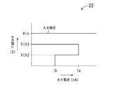
図1は、「アの字特性」方式を採用する過電流保護回路(以下、アの字方式という)を有するシリーズレギュレータの出力電圧を示すグラフである。図1において横軸は出力電流を示し、縦軸は出力電圧を示す。アの字方式では、電源が低電圧のときに、シリーズレギュレータの出力電圧を用いる電子機器の内部回路の動作が犠牲になってしまうという問題がある。アの字方式では、シリーズレギュレータの出力電圧を監視し、シリーズレギュレータの出力電圧が所定の電圧Vaよりも下回ると、出力電圧が得られなくなるので、制限電流がIaからIbに切り替わってしまう。つまり従来の方式では、過負荷によってシリーズレギュレータの出力電圧が低下したのか、シリーズレギュレータの定電圧動作によって出力電圧が低下したのかを、区別することができない。 FIG. 1 is a graph showing the output voltage of a series regulator having an overcurrent protection circuit (hereinafter referred to as “A-shaped method”) employing the “A-shaped characteristic” method. In FIG. 1, the horizontal axis indicates the output current, and the vertical axis indicates the output voltage. The A-shaped method has a problem that the operation of the internal circuit of the electronic device using the output voltage of the series regulator is sacrificed when the power supply is at a low voltage. In the A-shaped method, the output voltage of the series regulator is monitored, and when the output voltage of the series regulator is lower than the predetermined voltage Va, the output voltage cannot be obtained, so that the limit current is switched from Ia to Ib. In other words, in the conventional method, it cannot be distinguished whether the output voltage of the series regulator has dropped due to overload or whether the output voltage has fallen due to constant voltage operation of the series regulator.
たとえば車載品の場合、特に低温下や、老朽化バッテリを使用する場合には、エンジンの始動のためのスタータを回しているクランキング時などに、バッテリ電圧が大きく低下するが、エンジンの始動を完了するためには、バッテリ電圧が低下した状態であっても、電子機器の内部回路が噴射および点火などの最低限の処理動作をしなくてはならない。ところがバッテリ電圧が低下すると、同時にシリーズレギュレータの出力電圧も低下してしまうため、過電流保護回路が作用して、本来の電子機器の内部回路が成すべき動作まで制限されてしまうという問題がある。たとえば図1に仮想線で示す負荷線で動作するIC(Integrated Circuit)では、入力電圧が低いときには大きな入力電流を必要とするが、電源電圧が低下するとICの動作に必要な電流がICに入力されずに、動作が制限されてしまう。また特許文献1に記載される従来の技術においても、同様の問題がある。 For example, in the case of in-vehicle products, especially when the temperature is low or when an aging battery is used, the battery voltage decreases greatly during cranking when the starter is turned on to start the engine. In order to complete, the internal circuit of the electronic device must perform minimum processing operations such as injection and ignition even when the battery voltage is low. However, when the battery voltage decreases, the output voltage of the series regulator also decreases at the same time. Therefore, there is a problem that the overcurrent protection circuit acts and the operation that the internal circuit of the original electronic device should perform is limited. For example, an IC (Integrated Circuit) that operates on a load line indicated by a virtual line in FIG. 1 requires a large input current when the input voltage is low, but when the power supply voltage decreases, a current necessary for the operation of the IC is input to the IC Instead, the operation is limited. The conventional technique described in Patent Document 1 also has the same problem.
したがって本発明の目的は、ブーストランジスタを保護するだけではなく、電源電圧が低下したときであっても、出力電圧を用いる機器に所望の電流を供給することができるシリーズレギュレータおよびそれを備える電子機器を提供することである。 Accordingly, an object of the present invention is not only to protect the booth transistor but also to provide a series regulator that can supply a desired current to a device that uses the output voltage even when the power supply voltage drops, and an electronic device including the series regulator Is to provide.
本発明(1)は、入力部と、出力部と、入力部および出力部の間に設けられるブーストトランジスタとを備え、ブーストトランジスタを制御することによって、入力部に与えられる入力電圧を所定の電圧に変換して出力部から出力可能なシリーズレギュレータであって、
前記入力電圧を検出する検出部と、
前記入力電圧が予め定める第1電圧よりも高く、かつ前記出力部の電圧が予め定める第2の電圧よりも高いときに、前記出力部からの出力電流を予め定める電流に保持し、前記入力電圧が予め定める第1の電圧よりも高く、かつ前記出力部の電圧が予め定める第2の電圧よりも低くなると、前記出力部からの出力電流を低下させる第1の過電流制限特性と、前記入力電圧が前記予め定める第1の電圧よりも低い予め定める範囲の電圧で、かつ前記出力部の電圧が予め定める第2の電圧よりも低いときに、前記第1の過電流制限特性における出力電流よりも大きな出力電流を前記出力部から出力可能な第2の過電流制限特性とを切り換えて、前記ブーストトランジスタを制御する制御部とを備えることを特徴とするシリーズレギュレータである。
The present invention (1) includes an input unit, an output unit, and a boost transistor provided between the input unit and the output unit. By controlling the boost transistor, an input voltage applied to the input unit is set to a predetermined voltage. Series regulator that can convert to
A detection unit for detecting the input voltage;
When the input voltage is higher than a predetermined first voltage and the voltage of the output unit is higher than a predetermined second voltage, an output current from the output unit is held at a predetermined current, and the input voltage Is higher than a predetermined first voltage, and when the voltage of the output unit is lower than a predetermined second voltage, a first overcurrent limiting characteristic for reducing an output current from the output unit, and the input When the voltage is in a predetermined range lower than the predetermined first voltage and the voltage of the output unit is lower than the predetermined second voltage, the output current in the first overcurrent limiting characteristic is more than And a control unit that controls the boost transistor by switching to a second overcurrent limiting characteristic capable of outputting a large output current from the output unit.
また本発明(3)は、入力部と、出力部と、入力部および出力部の間に設けられるブーストトランジスタとを備え、ブーストトランジスタを制御することによって、入力部に与えられる入力電圧を所定の電圧に変換して出力部から出力可能なシリーズレギュレータであって、
前記入力電圧および前記出力部の電圧の電位差を検出する検出部と、
前記電位差が予め定める電位差よりも大きく、かつ前記出力部の電圧が予め定める電圧よりも高いときに、前記出力部からの出力電流を予め定める電流に保持し、前記入力電圧が予め定める電位差よりも高く、かつ前記出力部の電圧が予め定める電圧よりも低くなると、前記出力部からの出力電流を低下させる第1の過電流制限特性と、前記入力電圧が前記予め定める電位差よりも小さい予め定める範囲の電位差で、かつ前記出力部の電圧が予め定める電圧よりも低いときに、前記第1の過電流制限特性における出力電流よりも大きな出力電流を前記出力部から出力可能な第2の過電流制限特性とを切り換えて、前記ブーストトランジスタを制御する制御部とを備えることを特徴とするシリーズレギュレータである。
Further, the present invention (3) includes an input unit, an output unit, and a boost transistor provided between the input unit and the output unit. By controlling the boost transistor, an input voltage applied to the input unit is set to a predetermined value. A series regulator that can convert to voltage and output from the output section,
A detection unit for detecting a potential difference between the input voltage and the voltage of the output unit;
When the potential difference is larger than a predetermined potential difference and the voltage of the output unit is higher than a predetermined voltage, the output current from the output unit is held at a predetermined current, and the input voltage is larger than the predetermined potential difference. A first overcurrent limiting characteristic that reduces the output current from the output unit when the voltage of the output unit is lower than a predetermined voltage, and a predetermined range in which the input voltage is smaller than the predetermined potential difference And a second overcurrent limit capable of outputting an output current larger than the output current in the first overcurrent limit characteristic when the voltage of the output section is lower than a predetermined voltage. And a control unit that controls the boost transistor by switching characteristics.
また本発明(5)は、前記シリーズレギュレータを備えることを特徴とする電子機器である。 The present invention (5) is an electronic apparatus comprising the series regulator.
本発明(1)によれば、入力電圧を検出部によって検出し、この入力電圧に応じて制御部が、第1および第2の過電流制限特性を切り換えて、ブーストトランジスタを制御する。第1の過電流制限特性は、入力電圧が予め定める第1の電圧よりも高く、かつ出力部の電圧が予め定める第2の電圧よりも高いときには、出力部からの出力電流を予め定める電流に保持し、入力電圧が予め定める第1の電圧よりも高く、かつ出力部の電圧が予め定める第2の電圧よりも低くなると、出力部からの出力電流を低下させる特性である。第2の過電流制限特性は、入力電圧が予め定める第1の電圧よりも低い予め定める範囲の電圧で、かつ出力部の電圧が予め定める第2の電圧よりも低い場合に、第1の過電流制限特性における出力電流よりも大きな出力電流を出力部から出力することができる特性である。 According to the present invention (1), the input voltage is detected by the detection unit, and the control unit switches the first and second overcurrent limiting characteristics in accordance with the input voltage to control the boost transistor. The first overcurrent limiting characteristic is that when the input voltage is higher than the predetermined first voltage and the voltage of the output unit is higher than the predetermined second voltage, the output current from the output unit is set to the predetermined current. When the input voltage is higher than the predetermined first voltage and the voltage of the output unit is lower than the predetermined second voltage, the output current from the output unit is reduced. The second overcurrent limiting characteristic is the first overcurrent when the input voltage is a voltage in a predetermined range lower than the predetermined first voltage and the voltage of the output unit is lower than the predetermined second voltage. This is a characteristic that can output an output current larger than the output current in the current limiting characteristic from the output unit.
これによって入力電圧が予め定める第1の電圧よりも高いときには、出力電圧が予め定める第2の電圧よりも低下したときに、出力電流が制限されるので、地絡時にトランジスタのベースおよびコレクタ間の焼損を抑制することができるとともに、入力電圧が予め定める第1の電圧よりも低いときには、出力電圧が予め定める第2の電圧よりも低下したときに、出力部からの出力電流を、第1の過電流制限特性の場合に比べて増加させるようにブーストトランジスタが制御部によって制御されるので、入力電圧が低下したときであっても、出力電圧を用いる機器に所望の電流を供給することができる。したがって、高いフェールセーフ性と、低電圧時における動作とを両立することができる。 As a result, when the input voltage is higher than the predetermined first voltage, the output current is limited when the output voltage is lower than the predetermined second voltage. Burnout can be suppressed, and when the input voltage is lower than the predetermined first voltage, the output current from the output unit is changed to the first voltage when the output voltage is lower than the predetermined second voltage. Since the boost transistor is controlled by the control unit so as to increase compared to the case of the overcurrent limiting characteristic, a desired current can be supplied to a device using the output voltage even when the input voltage is lowered. . Therefore, both high fail-safety and operation at low voltage can be achieved.
本発明(3)によれば、入力電圧および出力部の電圧の電位差を検出部によって検出し、この電位差に応じて制御部が、第1および第2の過電流制限特性を切り換えて、ブーストトランジスタを制御する。第1の過電流制限特性は、前記電位差が予め定める電位差よりも大きく、かつ出力部の電圧が予め定める電圧よりも高いときには、出力部からの出力電流を予め定める電流に保持し、前記電位差が予め定める電位差よりも大きく、かつ出力部の電圧が予め定める電圧よりも低くなると、出力部からの出力電流を低下させる特性である。第2の過電流制限特性は、前記電位差が予め定める電位差よりも小さい予め定める範囲の電位差で、かつ出力部の電圧が予め定める電圧よりも低い場合に、第1の過電流制限特性における出力電流よりも大きな出力電流を出力部から出力することができる特性である。 According to the present invention (3), the potential difference between the input voltage and the voltage of the output unit is detected by the detection unit, and the control unit switches between the first and second overcurrent limiting characteristics according to the potential difference, and the boost transistor To control. In the first overcurrent limiting characteristic, when the potential difference is larger than a predetermined potential difference and the voltage of the output unit is higher than a predetermined voltage, the output current from the output unit is held at a predetermined current, and the potential difference is When the voltage difference is larger than the predetermined potential difference and the voltage of the output unit becomes lower than the predetermined voltage, the output current from the output unit is reduced. The second overcurrent limiting characteristic is an output current in the first overcurrent limiting characteristic when the potential difference is a potential difference in a predetermined range smaller than the predetermined potential difference and the voltage of the output unit is lower than the predetermined voltage. It is a characteristic that a larger output current can be output from the output unit.
これによって前記電位差が予め定める電位差よりも大きいときには、出力電圧が予め定める電圧よりも低下したときに、出力電流が制限されるので、地絡時にトランジスタのベースおよびコレクタ間の損失を低減することができるとともに、前記電位差が予め定める電圧よりも小さいときには、出力電圧が所定の電圧から低下したときに、出力部からの出力電流を、第1の過電流制限特性の場合に比べて増加させるようにブーストトランジスタが制御部によって制御されるので、入力電圧が低下したときであっても、出力電圧を用いる機器に所望の電流を供給することができる。したがって、高いフェールセーフ性と、低電圧時における動作とを両立することができる。 As a result, when the potential difference is larger than the predetermined potential difference, the output current is limited when the output voltage drops below the predetermined voltage, so that the loss between the base and collector of the transistor can be reduced during a ground fault. In addition, when the potential difference is smaller than a predetermined voltage, when the output voltage drops from a predetermined voltage, the output current from the output unit is increased as compared with the case of the first overcurrent limiting characteristic. Since the boost transistor is controlled by the control unit, a desired current can be supplied to a device using the output voltage even when the input voltage is lowered. Therefore, both high fail-safety and operation at low voltage can be achieved.
本発明(5)によれば、前記スイッチングレギュレータを備えることによって、ブーストトランジスタの焼損破壊が抑制されるとともに、スイッチングレギュレータに入力される入力電圧が低下したときに、スイッチングレギュレータから出力される電流の低下が抑制されるので、スイッチングレギュレータからの電流が与えられて動作する回路の動作が制限されてしまうことを抑制することができ、信頼性の向上された電子機器を提供することができる。 According to the present invention (5), by providing the switching regulator, the burnout destruction of the boost transistor is suppressed, and the current output from the switching regulator is reduced when the input voltage input to the switching regulator is reduced. Since the decrease is suppressed, it is possible to suppress the operation of a circuit that operates by being supplied with a current from the switching regulator, and an electronic device with improved reliability can be provided.
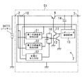
図2は、本発明の実施の一形態のシリーズレギュレータ1を示す回路図である。シリーズレギュレータ(以下、レギュレータという)1は、入力部2と、出力部3と、入力部2および出力部3の間に設けられるブーストトランジスタ(以下、出力トランジスタという)4とを備え、ブーストトランジスタ4を制御することによって、入力部2に与えられる入力電圧を所定の電圧に変換して出力部3から出力可能となっている。入力部2には電源であるバッテリ(BATT)5が接続されて、バッテリ5から電源電圧が与えられる。したがって本実施の形態において、レギュレータ1に与えられる入力電圧は、電源電圧(バッテリ電圧)に等しい。ブーストトランジスタ4は、PNP型のバイポーラトランジスタ(以下「PNPトランジスタ」という)であり、エミッタが後述する抵抗素子10を介して入力部2に電気的に接続され、コレクタが出力部3に電気的に接続されている。ブーストトランジスタ4は、そのベースに与えられる信号に応じて、エミッタに与えられる電圧を所定の電圧に変換して、コレクタから出力する。
FIG. 2 is a circuit diagram showing a series regulator 1 according to an embodiment of the present invention. A series regulator (hereinafter referred to as a regulator) 1 includes an
レギュレータ1は、電源電圧モニタ部6と、制御部7とを含んで構成されている。電源電圧モニタ部6は、入力電圧を検出する検出部である。電源電圧モニタ部6は、入力電圧と、予め定める第1の電圧Vth1とを比較して、その結果を後述する切り換え部16に与える。電源電圧モニタ部6は、たとえば入力電圧が予め定める第1の電圧Vth1以上のときには、ハイレベルの信号を出力して、入力電圧が予め定める第1の電圧Vth1未満のときには、ローレベルの信号を出力する。
The regulator 1 is configured to include a power supply
図3は、電源電圧モニタ部6の回路構成の一例を示す図である。電源電圧モニタ部6は、2つの直列に抵抗される抵抗素子7a,7bと、コンパレータ8と、第1の基準電圧源9とを備える。直列に接続される抵抗素子7a,7bの一方の端子は、入力部2に電気的に接続され、他方はグランドに電気的に接続される。コンパレータ8の非反転入力端子は、抵抗素子7a,7bの接続部位7cに接続され、反転入力端子は第1の基準電圧源9に接続される。コンパレータ8の出力端子が後述する切り換え部16の切り換え制御端子16dに電気的に接続される。第1の基準電圧源9の電圧は、予め定める第1の電圧Vth1である。
FIG. 3 is a diagram illustrating an example of a circuit configuration of the power supply
制御部7は、抵抗素子10と、第1および第2トランジスタ11,12と、レギュレータ制御回路13と、コンデンサ14と、切り換え部16と、複数の過電流制限特性を実現するための第1の過電流制御回路21および第2の過電流制御回路22とを備えている。第1の過電流制御回路21および第2の過電流制御回路22は、過電流からブートトランジスタ4を保護するための保護回路である。
The
抵抗素子10は、その一方の端子が入力部2に接続され、他方の端子がブーストトランジスタ4のエミッタに電気的に接続されている。第1トランジスタ11は、NPN型のバイポーラトランジスタ(以下「NPNトランジスタ」という)であり、エミッタがグランドに接続され、コレクタが、ブーストトランジスタ4のベースに接続され、ベースが、レギュレータ制御回路13に接続されている。
The
第2トランジスタ12は、NPNトランジスタであり、エミッタがグランドに接続され、コレクタが第1トランジスタ11のベースに接続され、ベースが、切り換え回路17に接続されている。レギュレータ制御回路13は、ブーストトランジスタ4のコレクタから出力される出力電圧を検知し、第1トランジスタ11のベースに供給する電流を変化させて、ブーストトランジスタ4のベース電流を制御し、ブーストトランジスタ4の出力電圧が所定の電圧になるように制御する。
The
コンデンサ14は、一方の端子がブーストトランジスタ4のコレクタに接続され、他方の端子がレギュレータ制御回路13に接続されている。コンデンサ14を設けることによって、ブーストトランジスタ4のコレクタから出力される出力電圧の急激な変動を抑制して、レギュレータ制御回路13においてブーストトランジスタ4のコレクタから出力される出力電圧を安定して検出することができる。
The
切り換え部16は、2つの入力端子16a,16bと、1つの出力端子16cと、切り換え制御端子16dを有する3端子スイッチによって構成されている。切り換え部16は、電源電圧モニタ部6から切り換え制御端子16dに与えられる信号に応じて、2つの入力端子16a,16bのうちの一方と、出力端子16cとを選択的に接続する。ここでは、電源電圧モニタ部6から与えられる信号がハイレベルのとき、入力端子16aと出力端子16cとを接続し、電源電圧モニタ部6から与えられる信号がローレベルのとき、入力端子16bと出力端子16cとを接続する。
The switching
第1の過電流制御回路21は、出力電圧が予め定める第2の電圧Vth2よりも高いときには、出力部3からの出力電流を予め定める電流に保持し、出力電圧が予め定める第2の電圧Vth2よりも低くなると、出力部3からの出力電流を低下させるような、指令信号を出力する。第1の過電流制御回路21は、3つの入力端子21a,21b,21cと、1つの出力端子21dとを備える。入力端子21aは、抵抗素子10の一端に電気的に接続され、入力端子21bは抵抗素子10の他端に電気的に接続され、入力端子21cはブーストトランジスタ4のコレクタに電気的に接続されている。出力端子21dは、切り換え部16の入力端子16aに電気的に接続されている。
When the output voltage is higher than the predetermined second voltage Vth2, the first
図4は、第1の過電流制御回路21の一例を示す図である。第1の過電流制御回路21は、抵抗素子31a,31b,31cと、コンパレータ32a,32bと、電流源33a,33bと、第2の基準電圧源34とを、制御スイッチ35とを備える。抵抗素子31aの一方の端子が入力端子21aに電気的に接続され、他方の端子がコンパレータ32aの非反転入力端子に接続されている。コンパレータ32aの反転入力端子は、入力端子21bに接続されている。コンパレータ32aの出力端子は、出力端子21dに接続されている。第2の基準電圧源34の電圧は、予め定める第2の電圧Vth2よりも低い電圧である、予め定める第3の電圧Vth3である。予め定める第1の電圧Vth1は、Vth2<Vth1<Vth3となるように設定されている。
FIG. 4 is a diagram illustrating an example of the first
抵抗素子31b,32cは、直列に接続され、直列に接続された抵抗素子31b,32cの一方の端子が入力端子21cに接続され、他方の端子がグランドに接続されている。コンパレータ32bの非反転入力端子は、抵抗素子31b,32cの接続部位に接続され、反転入力端子は第2の基準電圧源34に接続されている。コンパレータ32aの反転入力端子および抵抗素子31aの他方の端子には、電流源33aと、制御スイッチ35の一方の端子とが接続されている。制御スイッチ35の他方の端子には、電流源33bが接続される。制御スイッチ35の制御端子は、コンパレータ32bの出力端子に接続されている。
The
第1の過電流制御回路21では、入力端子21a,21b間に与えられる電圧と、入力端子21cに与えられる電圧とに応じて、制御スイッチ35が一方の接続端子と他方の接続端子との、導通および非導通を切り換えることによって、レギュレータ1から出力される電圧および電流特性が、いわゆる「アの字特性」となるように、出力端子21dから信号を出力する。
In the first
図5は、切り換え部16の入力端子16aと出力端子16cとが接続されているときの、レギュレータ1から出力される電圧および電流特性を示すグラフである。図5において、横軸は出力電流を示し、縦軸は出力電圧を示す。図5においては、予め定める第1の電圧Vthよりも大きな入力電圧Vinが入力されているとする。またレギュレータ1は、予め定める第1の電圧Vthよりも大きな入力電圧をVinが入力されているときには、出力電圧が、予め定める第3の電圧Vthとなるように出力電圧を調整する。図5に示すように、レギュレータ1は出力電圧をVoutとし、Vth3≧Vout≧Vth2のときには、出力電流をIaで一定に保持して過電流を抑制し、Vth3>Voutのときには、出力部3において短絡が発生しているおそれがあるので、出力電流をIaより小さなIbで、一定に保持して、出力部3に接続される回路を保護する。Vinは、たとえば14V程度であり、Vth2は、たとえば3V程度であり、Vth3はたとえば5V程度である。またIbはIaの1/2以下程度に設定されている。
FIG. 5 is a graph showing the voltage and current characteristics output from the regulator 1 when the
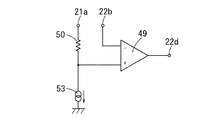
再び図2を参照して、第2の過電流制御回路22は、出力電圧が予め定める電圧Vth2よりも低い予め定める範囲の電圧のときに、第1の過電流制御回路21における出力電流よりも大きな出力電流を出力部3から出力させるような指令信号を出力する。第2の過電流制御回路22は、2つの入力端子22a,22bと、1つの出力端子22dとを備える。入力端子22aは、抵抗素子10の一端に電気的に接続され、入力端子22bは抵抗素子10の他端に電気的に接続されている。出力端子22dは、切り換え部16の入力端子16bに接続されている。
Referring again to FIG. 2, the second
図6は、第2の過電流制御回路22の一例を示す図である。第2の過電流制御回路22は、抵抗素子50と、コンパレータ49と、電流源53とを有する。抵抗素子50の一方の端子が入力端子22aに電気的に接続され、他方の端子がコンパレータ49の非反転入力端子に接続されている。コンパレータ49の反転入力端子は、入力端子22bに接続されている。コンパレータ49の出力端子は、出力端子22dに接続されている。コンパレータ49の反転入力端子および抵抗素子50の他方の端子には、電流源53が接続されている。
FIG. 6 is a diagram illustrating an example of the second
第2の過電流制御回路22では、入力端子22a,22b間に与えられる電圧に応じて、レギュレータ1から出力される電圧および電流特性が、いわゆる「垂下特性」となるように、出力端子22dから信号を出力する。
In the second
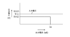
図7は、切り換え部16の入力端子16bと出力端子16cとが接続されているときの、レギュレータ1から出力される電圧および電流特性を示すグラフである。図7において、横軸は出力電流を示し、縦軸は出力電圧を示す。図5においては、予め定める第1の電圧Vthよりも大きな入力電圧Vinが入力されているとする。レギュレータ1は、予め定める第1の電圧Vthよりも小さな入力電圧Vinが入力されているときには、出力電圧が、予め定める第2の電圧Vth2となるように出力電圧を調整する。図7に示すように、レギュレータ1は出力電圧をVoutとし、Vth2≧Voutのときには、出力電流をIaで一定に保持して過電流を抑制する。
FIG. 7 is a graph showing the voltage and current characteristics output from the regulator 1 when the
以上のようにレギュレータ1では、入力電圧が予め定める第1の電圧Vth1よりも大きい場合と小さい場合とにおいて、第1の過電流制御回路21および第2の過電流制御回路22を選択的に第2トランジスタ12に電気的に接続して、図5と図7に示すような出力電圧電流特性とを切り換えて、出力電圧と出力電流とを制御している。これによって入力電圧が予め定める第1の電圧Vth1よりも高いときには、出力電圧が予め定める第2の電圧Vth2から低下したときに、出力電流が制限されるので、地絡時にブーストトランジスタ4のベースおよびコレクタ間の焼損を抑制することができるとともに、入力電圧が予め定める電圧よりも低いときには、出力電圧が予め定める第2の電圧Vth2よりも低下したときに、出力部からの出力電流を、第1の過電流制限特性の場合に比べて増加させるようにブーストトランジスタ4が制御部7によって制御されるので、入力電圧が低下したときであっても、出力電圧を用いる機器に所望の電流を供給することができる。したがって、高いフェールセーフ性と、低電圧時における動作とを両立することができる。
As described above, in the regulator 1, the first
本実施の形態では、第1の過電流制御回路21をアの字特性の保護回路としているが、第1の過電流制御回路21のフの字特性の保護回路としてもよい。フの字特性の保護回路を用いると、出力電圧が低下したときに、出力電流を線形に変化させることができる。このような組合せであっても、前述した実施の形態と同様の効果を達成することができる。
In the present embodiment, the first
図8は、本発明の実施の他の形態のレギュレータ41を示す回路図である。本実施の形態のレギュレータ41は、前述の図2に示すレギュレータ1に類似し、基本的には、前述の図2に示すレギュレータ1の構成に、第3の過電流制御回路23を付加した構成であるので、同様の構成には同様の参照符号を付して、重複する説明を省略する。電源電圧モニタ部6は、入力電圧と、予め定める第1の電圧Vth1とを比較し、さらに入力電圧と、予め定める第1の電圧Vth1よりも低い予め定める第4の電圧Vth4とを比較して、その結果を後述する切り換え部16に与える。電源電圧モニタ部6は、たとえば2つの出力端子を備え、たとえば入力電圧が予め定める第1の電圧Vth1以上のときには、一方の出力端子からハイレベルの信号を出力して、入力電圧が予め定める第1の電圧Vth1未満のときには、一方の出力端子からローレベルの信号を出力し、たとえば入力電圧が予め定める第4の電圧Vth4以上のときには、他方の出力端子からハイレベルの信号を出力して、入力電圧が予め定める第4の電圧Vth4未満のときには、他方の出力端子からローレベルの信号を出力する。
FIG. 8 is a circuit diagram showing a
本実施の形態では、切り換え部16は、2つの入力端子16a,16bと、1つの出力端子16cと、切り換え制御端子16dとに加えて、さらに1つの入力端子16eとを有するスイッチによって構成されている。切り換え部16は、電源電圧モニタ部6から切り換え制御端子16dに与えられる信号に応じて、3つの入力端子16a,16b,16eのうちのいずれか1つと、出力端子16cとを選択的に接続する。ここでは、電源電圧モニタ部6の一方の出力端子から与えられる信号がハイレベルで、かつ他方の出力端子から与えられる信号レベルがハイレベルとき、入力端子16aと出力端子16cとを接続し、一方の出力端子から与えられる信号がローレベルで、かつ他方の出力端子から与えられる信号レベルがハイレベルとき、入力端子16eと出力端子16cとを接続し、一方の出力端子から与えられる信号がローレベルで、かつ他方の出力端子から与えられる信号レベルがローレベルとき、入力端子16bと出力端子16cとを接続する。
In the present embodiment, the switching
第1および第2の過電流制御回路21,22は、前述の実施の形態と同様であり、第3の過電流制御回路23は、3つの入力端子23a,23b,23cと、1つの出力端子23dとを備え、レギュレータ1から出力される電圧および電流特性が、いわゆる「フの字特性」となるように、出力端子23dから信号を出力する。すなわちレギュレータ41では、入力電圧が低下していくと、レギュレータ41の出力電圧電流特性が、アの字特性から、フの字特性に変化し、さらに垂下特性に変化する。このように、入力電圧に応じて、複数段階に特性を変化させることによって、出力部3に接続される付加において用いられる電流について、より細かな調整が可能となる。したがって、出力電圧と出力電流を負荷回路に応じて好適に変化させることができ、負荷回路における動作処理を円滑に行うことができる。
The first and second
図9は、本発明のさらに実施の他の形態のレギュレータ51を示す回路図である。本実施の形態のレギュレータ51は、前述の図2に示すレギュレータ1に類似し、基本的には、前述の図2に示すレギュレータ1の構成において、電源電圧モニタ部6を、差電圧モニタ部52に代えた構成を有し、その他の構成は、レギュレータ1と同様であるので、同様の構成には同様の参照符号を付して、重複する説明を省略する。
FIG. 9 is a circuit diagram showing a
差電圧モニタ部52は、入力部2に与えられる入力電圧と、出力部3の出力電圧との電位差を検出して、この電位差に応じて、切り換え制御端子16dに制御信号を与える。差電圧モニタ部52が検出した電位差が、予め定める電位差以上であれば、差電圧モニタ部52は、切り換え部16の入力端子16aと出力端子16cとを接続させ、前記電位差が、予め定める電位差未満であれば、差電圧モニタ部52は、切り換え部16の入力端子16bと出力端子16cとを接続させる。
The differential
以上のようなレギュレータ51においても、前述したレギュレータ1と同様の効果を達成することができる。また入力電圧と出力電圧との電位差に基づいて、出力電圧電流特性を切り換えるので、電源電圧モニタ部6では必要である第1の基準電圧源9を用いなくても回路を構成することができ、回路構成を簡略化することができる。
In the
図10は、本発明の実施のさらに他の形態のレギュレータ61を示す回路図である。本実施の形態のレギュレータ61は、前述の図2に示すレギュレータ1に類似し、基本的には、前述の図2に示すレギュレータ1の構成において、第1および第2の過電流制御回路21,22と切り換え部16とを、アの字保護回路62に代えた構成であるので、同様の構成には同様の参照符号を付して、その説明を省略する。
FIG. 10 is a circuit diagram showing a
アの字保護回路62は、3つの入力端子21a,21b,21cと、1つの出力端子21dとを備え、レギュレータ61から出力される電圧および電流特性が、アの字特性となるように出力端子21dから信号を出力する。
The
図11は、レギュレータ61から出力される電圧および電流特性を示すグラフである。レギュレータ61は、入力電圧Vinが予め定める電圧VT以上のときに、アの字特性における電流の切り替える電圧レベルをV1とし、入力電圧Vinが予め定める電圧VT未満のときに、アの字特性における電流を切り替える電圧レベルをVth2よりも低いVth4とする。したがってレギュレータ61では、アの字特性で、電圧レベルがV1となる第1の過電流制限特性と、アの字特性で、電圧レベルがV2となる第2の過電流制限特性が切り換えられる。したがって、第2の過電流制限特性は、第1の過電流制限特性において出力部3からの出力電流を低下させる基準となる予め定める電圧VTを低下させた特性となり、すなわち出力部の電圧が予め定める第2の電圧Vth2以下、かつ予め定めるしきい電圧Vth4を超えるときに、出力部3からの出力電流を予め定める電流に保持し、出力部3の電圧が予め定めるしきい電圧Vth4未満になると、出力部3からの出力電流を低下させる特性となる。
FIG. 11 is a graph showing the voltage and current characteristics output from the
図12は、アの字保護回路62の一例を示す回路図である。図4に示す第1の過電流制御回路21の構成に加えて、抵抗素子64と、スイッチ素子65とを備えて構成されている。抵抗素子64は、抵抗素子31cと、グランドとの間に介在され、スイッチ素子65は、抵抗素子31cと並列に接続されている。スイッチ素子65の一方の端子は、抵抗素子31cと抵抗素子64との接続部位に接続され、他方の端子はグランドに接続されている。スイッチ素子65は、電源電圧モニタ部6からの制御信号に応じて、開閉し、電源電圧モニタ部6からハイレベルの信号が与えられるとスイッチが閉じた状態となり、電源電圧モニタ部6からハイレベルの信号が与えられるとスイッチが開いた状態となる。スイッチ素子65の開閉に応じて、コンパレータ32bの非反転入力端子に入力される電圧が変化する。これによって、アの字特性における電流の切り替える電圧レベルをV1からV2に変化させることができる。
FIG. 12 is a circuit diagram showing an example of the letter
抵抗素子31b,31c,64と、コンパレータ32bと、電流源33a,33bと、第2の基準電圧源34とを、制御スイッチ35と、スイッチ素子65とを備えて、過電流検知レベル切換回路部63が構成されている。以上のようなレギュレータ61においても、前述したレギュレータ1と同様の効果を達成することができる。
The
図13は、本発明の実施のさらに他の形態のレギュレータ71を示す回路図である。本実施の形態のレギュレータ71は、前述の図2および図10に示すレギュレータ1に類似し、基本的には、前述の図10に示すレギュレータ1の構成において、アの字保護回路62を、他のアの字保護回路72に代えた構成であるので、同様の構成には同様の参照符号を付して、その説明を省略する。
FIG. 13 is a circuit diagram showing a
図10に示す実施の形態では、第2の過電流制限特性は、第1の過電流制限特性において出力部3からの出力電流を低下させる基準となる予め定める電圧VTを低下させた特性としているが、本実施の形態では、第2の過電流制限特性は、第1の過電流制限特性において入力電圧が予め定める電圧VTよりも低くなったときに、出力部3から出力される出力電流を増加させた特性となっている。
In the embodiment shown in FIG. 10, the second overcurrent limiting characteristic is a characteristic in which a predetermined voltage VT that is a reference for reducing the output current from the
図14は、レギュレータ71から出力される電圧および電流特性を示すグラフである。レギュレータ71は、入力電圧Vinが予め定める電圧VT以上のときに、アの字特性における電流の制限レベル(Ib)を、第1の制限レベルIb1とし、入力電圧Vinが予め定める電圧VT未満のときに、アの字特性における電流の制限レベルをIb1よりも大きい第2の制限レベルIb2とする。したがってレギュレータ71では、アの字特性で、電圧レベルがV1となる第1の過電流制限特性と、アの字特性で、電圧レベルがV2となる第2の過電流制限特性が切り換えられる。したがって、第2の過電流制限特性は、第1の過電流制限特性において出力電圧が予め定める第2の電圧Vth2よりも低くなったときに、出力部3から出力される出力電流を増加させた特性となり、すなわち、出力部3の電圧が予め定める第2の電圧Vth2以上のときに、出力部3からの出力電流を予め定める電流に保持し、出力部3の電圧が予め定める第2の電圧Vth2よりも低いときに、出力部3からの出力電流を予め定める電流よりも大きな電流に保持する特性となる。以上のようなレギュレータ51においても、前述したレギュレータ1と同様の効果を達成することができる。
FIG. 14 is a graph showing the voltage and current characteristics output from the
本発明の実施のさらの他の形態では、前述した図12および図13に示す回路を組み合わせて、レギュレータを構成してもよい。アの字特性における電流を切り替える電圧レベルと、アの字特性における電流の制限レベルとを設けることによって、接続される負荷にさらに最適な電流を出力部3から出力することができるようになる。
In still another embodiment of the present invention, a regulator may be configured by combining the circuits shown in FIGS. 12 and 13 described above. By providing the voltage level for switching the current in the A-shaped characteristic and the current limit level in the A-shaped characteristic, it becomes possible to output a further optimal current from the
また前述した図12に示すアの字保護回路62において、コンパレータ32bにヒステリシス特性を持たせるか、またはコンパレータ32bの出力にフィルタを挿入することによって、切り換え時のチャタリングを抑制する構成としてもよい。これによってチャタリングによって出力電圧電流特性が変化してしまうことが抑制され、レギュレータの信頼性を向上することができる。
Further, in the above-described character-shaped
上述した各実施の形態では、レギュレータの入力部2をバッテリ5に接続しているが、入力部2は、本発明の各実施の形態のいずれかのレギュレータの出力部3に接続されて、レギュレータを多段に接続してもちいてもよい。
In each of the above-described embodiments, the
また上述した各実施の形態のレギュレータのいずれかを備える電子機器においては、前記レギュレータを備えることによって、ブーストトランジスタの焼損破壊が抑制されるとともに、スイッチングレギュレータに入力される入力電圧が低下したときに、レギュレータから出力される電流の低下が抑制されるので、レギュレータからの電流が与えられて動作する回路の動作が制限されてしまうことを抑制することができる。したがって、信頼性の向上された電子機器を提供することができる。 In addition, in an electronic device including any of the regulators of the above-described embodiments, by providing the regulator, burnout destruction of the boost transistor is suppressed and the input voltage input to the switching regulator is reduced. Since the decrease in the current output from the regulator is suppressed, it is possible to suppress the operation of the circuit that operates by being supplied with the current from the regulator. Therefore, an electronic device with improved reliability can be provided.
1,41,51,61,71 シリーズレギュレータ
2 入力部
3 出力部
4 ブーストトランジスタ
6 電源電圧モニタ部
7 制御部
21 第1の過電流制御回路
22 第2の過電流制御回路
23 第3の過電流制御回路
52 差電圧モニタ部
62,72 アの字保護回路
1, 41, 51, 61, 71
Claims (5)
前記入力電圧を検出する検出部と、
前記入力電圧が予め定める第1電圧よりも高く、かつ前記出力部の電圧が予め定める第2の電圧よりも高いときに、前記出力部からの出力電流を予め定める電流に保持し、前記入力電圧が予め定める第1の電圧よりも高く、かつ前記出力部の電圧が予め定める第2の電圧よりも低くなると、前記出力部からの出力電流を低下させる第1の過電流制限特性と、前記入力電圧が前記予め定める第1の電圧よりも低い予め定める範囲の電圧で、かつ前記出力部の電圧が予め定める第2の電圧よりも低いときに、前記第1の過電流制限特性における出力電流よりも大きな出力電流を前記出力部から出力可能な第2の過電流制限特性とを切り換えて、前記ブーストトランジスタを制御する制御部とを備えることを特徴とするシリーズレギュレータ。 An input unit, an output unit, and a boost transistor provided between the input unit and the output unit are provided, and by controlling the boost transistor, an input voltage applied to the input unit is converted into a predetermined voltage to be output from the output unit. A series regulator capable of output,
A detection unit for detecting the input voltage;
When the input voltage is higher than a predetermined first voltage and the voltage of the output unit is higher than a predetermined second voltage, an output current from the output unit is held at a predetermined current, and the input voltage Is higher than a predetermined first voltage, and when the voltage of the output unit is lower than a predetermined second voltage, a first overcurrent limiting characteristic for reducing an output current from the output unit, and the input When the voltage is in a predetermined range lower than the predetermined first voltage and the voltage of the output unit is lower than the predetermined second voltage, the output current in the first overcurrent limiting characteristic is more than And a control unit that controls the boost transistor by switching to a second overcurrent limiting characteristic capable of outputting a larger output current from the output unit.
前記入力電圧および前記出力部の電圧の電位差を検出する検出部と、
前記電位差が予め定める電位差よりも大きく、かつ前記出力部の電圧が予め定める電圧よりも高いときに、前記出力部からの出力電流を予め定める電流に保持し、前記入力電圧が予め定める電位差よりも高く、かつ前記出力部の電圧が予め定める電圧よりも低くなると、前記出力部からの出力電流を低下させる第1の過電流制限特性と、前記入力電圧が前記予め定める電位差よりも小さい予め定める範囲の電位差で、かつ前記出力部の電圧が予め定める電圧よりも低いときに、前記第1の過電流制限特性における出力電流よりも大きな出力電流を前記出力部から出力可能な第2の過電流制限特性とを切り換えて、前記ブーストトランジスタを制御する制御部とを備えることを特徴とするシリーズレギュレータ。 An input unit, an output unit, and a boost transistor provided between the input unit and the output unit are provided, and by controlling the boost transistor, an input voltage applied to the input unit is converted into a predetermined voltage to be output from the output unit. A series regulator capable of output,
A detection unit for detecting a potential difference between the input voltage and the voltage of the output unit;
When the potential difference is larger than a predetermined potential difference and the voltage of the output unit is higher than a predetermined voltage, the output current from the output unit is held at a predetermined current, and the input voltage is larger than the predetermined potential difference. A first overcurrent limiting characteristic that reduces the output current from the output unit when the voltage of the output unit is lower than a predetermined voltage, and a predetermined range in which the input voltage is smaller than the predetermined potential difference And a second overcurrent limit capable of outputting an output current larger than the output current in the first overcurrent limit characteristic when the voltage of the output section is lower than a predetermined voltage. And a control unit that controls the boost transistor by switching characteristics.
Priority Applications (1)
| Application Number | Priority Date | Filing Date | Title |
|---|---|---|---|
| JP2008147494A JP2009294883A (en) | 2008-06-04 | 2008-06-04 | Series regulator and electronic equipment |
Applications Claiming Priority (1)
| Application Number | Priority Date | Filing Date | Title |
|---|---|---|---|
| JP2008147494A JP2009294883A (en) | 2008-06-04 | 2008-06-04 | Series regulator and electronic equipment |
Publications (1)
| Publication Number | Publication Date |
|---|---|
| JP2009294883A true JP2009294883A (en) | 2009-12-17 |
Family
ID=41543020
Family Applications (1)
| Application Number | Title | Priority Date | Filing Date |
|---|---|---|---|
| JP2008147494A Withdrawn JP2009294883A (en) | 2008-06-04 | 2008-06-04 | Series regulator and electronic equipment |
Country Status (1)
| Country | Link |
|---|---|
| JP (1) | JP2009294883A (en) |
Cited By (5)
| Publication number | Priority date | Publication date | Assignee | Title |
|---|---|---|---|---|
| JP2011166987A (en) * | 2010-02-12 | 2011-08-25 | Fuji Electric Co Ltd | Power supply apparatus |
| JP2013130937A (en) * | 2011-12-20 | 2013-07-04 | Ricoh Co Ltd | Constant voltage circuit and electronic equipment |
| JP2014100063A (en) * | 2014-03-03 | 2014-05-29 | Fuji Electric Co Ltd | Power supply device |
| JP2017120568A (en) * | 2015-12-28 | 2017-07-06 | ローム株式会社 | Power supply circuit and control circuit thereof, control method, and electronic equipment using the same |
| JP2020087306A (en) * | 2018-11-30 | 2020-06-04 | 株式会社デンソーテン | Voltage converter apparatus |
-
2008
- 2008-06-04 JP JP2008147494A patent/JP2009294883A/en not_active Withdrawn
Cited By (6)
| Publication number | Priority date | Publication date | Assignee | Title |
|---|---|---|---|---|
| JP2011166987A (en) * | 2010-02-12 | 2011-08-25 | Fuji Electric Co Ltd | Power supply apparatus |
| JP2013130937A (en) * | 2011-12-20 | 2013-07-04 | Ricoh Co Ltd | Constant voltage circuit and electronic equipment |
| JP2014100063A (en) * | 2014-03-03 | 2014-05-29 | Fuji Electric Co Ltd | Power supply device |
| JP2017120568A (en) * | 2015-12-28 | 2017-07-06 | ローム株式会社 | Power supply circuit and control circuit thereof, control method, and electronic equipment using the same |
| JP2020087306A (en) * | 2018-11-30 | 2020-06-04 | 株式会社デンソーテン | Voltage converter apparatus |
| JP7152942B2 (en) | 2018-11-30 | 2022-10-13 | 株式会社デンソーテン | voltage converter |
Similar Documents
| Publication | Publication Date | Title |
|---|---|---|
| US7408755B1 (en) | Advanced inrush/transient current limit and overload/short circuit protection method and apparatus for DC voltage power supply | |
| US8508900B2 (en) | Overvoltage protection circuit and electronic device comprising the same | |
| US8502513B2 (en) | Voltage regulator | |
| JP2011055634A (en) | Power supply breaker and electronic apparatus | |
| JP2004046616A (en) | Power circuit | |
| US20100027180A1 (en) | Electronic circuit breaker apparatus and systems | |
| JP2008197892A (en) | Series regulator | |
| JP2012231407A (en) | Semiconductor switching element drive circuit | |
| US10615586B2 (en) | Overcurrent protection device and vehicular electronic control unit | |
| JP2011061966A (en) | Voltage regulator | |
| JP2007244147A (en) | Power source protective circuit for integrated circuit | |
| JP2017045096A (en) | Semiconductor integrated circuit for regulator | |
| KR100782425B1 (en) | A charging circuit and a semiconductor device including the same | |
| JP2009294883A (en) | Series regulator and electronic equipment | |
| JP2015171224A (en) | power supply device | |
| JPS6154874A (en) | Power supply circuit device to electric load | |
| US9397493B2 (en) | Switching device | |
| US8593120B2 (en) | Voltage regulator | |
| US11281246B2 (en) | Circuit for detecting circuit defects and for preventing overvoltages in controllers | |
| JP2010015471A (en) | Regulator apparatus, and electronic apparatus provided with the same | |
| US20130119957A1 (en) | Bi-directional Switching Regulator and Control Circuit Thereof | |
| TWI695246B (en) | Voltage regulator | |
| TWI762133B (en) | Inrush current suppression circuit | |
| US11709514B2 (en) | Voltage regulator and in-vehicle backup power supply | |
| JP2014021634A (en) | Rush current suppression circuit |
Legal Events
| Date | Code | Title | Description |
|---|---|---|---|
| A300 | Withdrawal of application because of no request for examination |
Free format text: JAPANESE INTERMEDIATE CODE: A300 Effective date: 20110906 |