JP2009294167A - Image forming apparatus - Google Patents
Image forming apparatus Download PDFInfo
- Publication number
- JP2009294167A JP2009294167A JP2008150487A JP2008150487A JP2009294167A JP 2009294167 A JP2009294167 A JP 2009294167A JP 2008150487 A JP2008150487 A JP 2008150487A JP 2008150487 A JP2008150487 A JP 2008150487A JP 2009294167 A JP2009294167 A JP 2009294167A
- Authority
- JP
- Japan
- Prior art keywords
- connector
- temperature
- temperature sensor
- thermistor
- image forming
- Prior art date
- Legal status (The legal status is an assumption and is not a legal conclusion. Google has not performed a legal analysis and makes no representation as to the accuracy of the status listed.)
- Withdrawn
Links
Images


Classifications
-
- G—PHYSICS
- G03—PHOTOGRAPHY; CINEMATOGRAPHY; ANALOGOUS TECHNIQUES USING WAVES OTHER THAN OPTICAL WAVES; ELECTROGRAPHY; HOLOGRAPHY
- G03G—ELECTROGRAPHY; ELECTROPHOTOGRAPHY; MAGNETOGRAPHY
- G03G15/00—Apparatus for electrographic processes using a charge pattern
- G03G15/20—Apparatus for electrographic processes using a charge pattern for fixing, e.g. by using heat
- G03G15/2003—Apparatus for electrographic processes using a charge pattern for fixing, e.g. by using heat using heat
- G03G15/2014—Apparatus for electrographic processes using a charge pattern for fixing, e.g. by using heat using heat using contact heat
- G03G15/2039—Apparatus for electrographic processes using a charge pattern for fixing, e.g. by using heat using heat using contact heat with means for controlling the fixing temperature
Landscapes
- Physics & Mathematics (AREA)
- General Physics & Mathematics (AREA)
- Fixing For Electrophotography (AREA)
- Control Or Security For Electrophotography (AREA)
Abstract
【課題】 サーミスタ202の自己発熱を抑えながら、サーミスタ202からの信号の信号線上の電流値を増加させ、導通性能の向上、対ノイズ耐性の向上、及びコネクタ部201に形成されてしまった酸化皮膜の溶融除去を行う。
【解決手段】 定着ユニット40と画像形成装置本体とを接続するコネクタ部201に対して定着ユニット40内のサーミスタ202側に、サーミスタ202と並列に抵抗体301を接続し、抵抗体301の抵抗値を、定着ユニット40の低温時でもコネクタ部201の酸化皮膜を溶融除去できるような電流が流れるような値とする。
【選択図】 図4PROBLEM TO BE SOLVED: To increase a current value on a signal line of a signal from a thermistor 202 while suppressing self-heating of the thermistor 202, to improve conduction performance, to improve noise resistance, and an oxide film formed on a connector part 201 The melt is removed.
A resistor 301 is connected in parallel with the thermistor 202 on the side of the thermistor 202 in the fixing unit 40 with respect to a connector portion 201 that connects the fixing unit 40 and the image forming apparatus main body. Is set to such a value that a current flows that can melt and remove the oxide film of the connector portion 201 even when the fixing unit 40 is at a low temperature.
[Selection] Figure 4
Description
本発明は、電子写真プロセス方式を用いた複写機或いはプリンタ等の画像形成装置に於いて、信号経路および信号接続部における導通状態を改善する制御装置に関する。 The present invention relates to a control device for improving a conduction state in a signal path and a signal connection part in an image forming apparatus such as a copying machine or a printer using an electrophotographic process system.
画像形成装置における定着器の温度を検出する手段として、サーミスタが多く用いられている。定着装置の温度を検出するために、サーミスタは定着装置の内部に設けられ、信号信号線およびコネクタを介してCPU等の制御部へ検知信号が伝達されるように構成される。 A thermistor is often used as a means for detecting the temperature of a fixing device in an image forming apparatus. In order to detect the temperature of the fixing device, the thermistor is provided inside the fixing device and configured to transmit a detection signal to a control unit such as a CPU via a signal signal line and a connector.
そして制御部は、サーミスタからの検知信号に基づいて、定着装置を所定の温度に制御している。 The control unit controls the fixing device to a predetermined temperature based on the detection signal from the thermistor.
このような定着装置に適用するサーミスタは、転写材上のトナーを加熱定着させる温度、すなわち高温領域での温度検出を主目的としている為、その高温付近において精度が出るように構成されており、その抵抗値は数百Ω〜数キロΩ程度であることが多い。そして室温付近など低温領域における精度は荒く、その低温領域における抵抗値は、数百〜数メガΩ程度であることが多い。 The thermistor applied to such a fixing device is mainly configured to detect a temperature at which the toner on the transfer material is heated and fixed, that is, a temperature in a high temperature region, and is configured so that accuracy is obtained in the vicinity of the high temperature. The resistance value is often about several hundred Ω to several kiloΩ. The accuracy in the low temperature region such as near room temperature is rough, and the resistance value in the low temperature region is often about several hundred to several mega Ω.
上述のような特性の都合上、定着装置の温度が低い場合は、サーミスタの抵抗値が高いために、サーミスタが接続される信号線およびコネクタには、微少な電流(μAオーダー)しか流れないことになる。その場合には、下記のような課題が生ずる。 Due to the above characteristics, when the temperature of the fixing device is low, the resistance value of the thermistor is high, so that only a minute current (μA order) flows through the signal line and the connector to which the thermistor is connected. become. In that case, the following problems arise.
サーミスタが接続される信号線に微少な電流しか流れない為、その信号線に対して外乱ノイズが加わった場合に、信号線上のサーミスタの検知信号が乱れやすい。そして、サーミスタの検知信号に乱れが発生すると、定着装置の温度を誤って認識することになる。 Since a very small current flows through the signal line to which the thermistor is connected, the detection signal of the thermistor on the signal line is likely to be disturbed when disturbance noise is applied to the signal line. When the detection signal of the thermistor is disturbed, the temperature of the fixing device is erroneously recognized.
また、コネクタを互いに嵌合または結合させない状態で放置しておくと、コネクタのピンのメッキの状態によっては、その表面に酸化皮膜が形成されてしまうことがある。そして、コネクタのピンに酸化皮膜が形成された場合、コネクタを互いに嵌合させて通電を行っても、流れる電流の値が低いためにピンの酸化皮膜を破壊できず、電気的接続が得られないことになる。 Further, if the connectors are left in a state where they are not fitted or coupled to each other, an oxide film may be formed on the surface depending on the plating state of the pins of the connector. When an oxide film is formed on the connector pins, even if the connectors are fitted to each other and energized, the current value of the flowing current is low, so the pin oxide film cannot be destroyed and electrical connection can be obtained. There will be no.
上記のようにして、サーミスタの電気的接続が得られない場合や、サーミスタからの信号の伝送経路にノイズが重畳された場合、本来の検知温度よりも高い温度あるいは低い温度を検知することになる。 As described above, when electrical connection of the thermistor cannot be obtained, or when noise is superimposed on the transmission path of a signal from the thermistor, a temperature higher or lower than the original detection temperature is detected. .
誤って高い温度と検知した場合は、定着装置が本来の目標温度よりも低い温度に制御され、転写材上のトナー画像の定着不良が発生する等、画像品位の低下を招いてしまう。また誤って低い温度と検知した場合は、定着装置が本来の目標温度よりも高い温度に制御されるので、定着装置の劣化を早めてしまう等の課題を招いてしまう。 If it is erroneously detected as a high temperature, the fixing device is controlled to a temperature lower than the original target temperature, causing a poor fixing of the toner image on the transfer material, leading to a reduction in image quality. If the temperature is erroneously detected, the fixing device is controlled to a temperature higher than the original target temperature, which causes problems such as deteriorating the fixing device.
そこで、酸化皮膜によるコネクタの接触不良を回避するために、下記の方策が考えられている。
1.酸化しにくい材料(例えば、金)でコネクタピンをメッキする
2.コネクタを互いに嵌合させたときにコネクタピン同士が擦れて相互に相手側の表面を傷つけることで酸化被膜を破壊するような形状/構造にコネクタを形成する(参考文献1)。
3.コネクタを互いに嵌合させた後に、接点の酸化皮膜を破壊しうる電流を流して接触不良を解消する(参考文献2)。
Therefore, in order to avoid poor contact of the connector due to the oxide film, the following measures are considered.
1. 1. Plate the connector pins with a material that is difficult to oxidize (eg, gold). When the connectors are fitted to each other, the connector pins are rubbed to form a structure / structure that destroys the oxide film by damaging the mating surfaces of each other (Reference 1).
3. After fitting the connectors to each other, a current that can destroy the oxide film of the contact is passed to eliminate the contact failure (Reference Document 2).
また後述の、サーミスタの信号線上の外乱ノイズの影響を受けにくいようにするためには、ノイズ源となる他の信号線との距離を取ることや、サーミスタからの信号をアンプ等でバッファリングして伝達する等の方策が考えられる。
しかしながら、金等の酸化しにくい材料は高価なので、そのような材料を使用したコネクタでは、コストの面でデメリットが大きい。また、嵌合時にコネクタの表面を傷つけることで酸化被膜を破壊する構造のコネクタは、着脱を繰り返すと、本来導通すべき接点部自身が欠損してしまう為、例えばユーザによって繰り返し着脱される部位のコネクタとしては適していないと考えられる。 However, since materials that are difficult to oxidize such as gold are expensive, a connector using such a material has a large disadvantage in terms of cost. In addition, a connector having a structure that destroys the oxide film by damaging the surface of the connector at the time of mating causes the contact part itself to be conducted to be lost when it is repeatedly attached and detached. It seems that it is not suitable as a connector.
そこで、電流を流すことで酸化皮膜を破壊する回路が実用化されているが、サーミスタに代表される温度検知デバイスが接続される場合、電流を増加させると温度検知デバイスの自己発熱によって、温度検出の精度を損なってしまうという問題がある。 Therefore, a circuit that breaks down the oxide film by applying an electric current has been put into practical use. However, when a temperature detection device typified by a thermistor is connected, if the current is increased, the temperature detection device detects the temperature by self-heating of the temperature detection device. There is a problem that the accuracy of the system is impaired.
例えば、画像形成装置の定着装置におけるサーミスタの場合、サーミスタが自己発熱した分だけ、検出温度が高くなり、定着装置が本来の目標温度よりも低い温度に制御され、転写材上のトナー画像の定着不良が発生する等、画像品位の低下を招いてしまう。 For example, in the case of a thermistor in a fixing device of an image forming apparatus, the detection temperature is increased by the amount of self-heating of the thermistor, the fixing device is controlled to a temperature lower than the original target temperature, and the toner image on the transfer material is fixed. Deterioration of image quality such as occurrence of defects will be caused.
また、サーミスタの信号線上の外乱ノイズの影響を受けにくいようにするために、ノイズ源となる他の信号線との距離を取ることは、装置の小型化を妨げる要因となる。 Further, in order to make it less susceptible to disturbance noise on the signal line of the thermistor, taking a distance from other signal lines serving as noise sources becomes a factor that hinders downsizing of the apparatus.
また、サーミスタの信号をアンプ等でバッファリングして伝達する場合には、その回路のコスト増加や電装スペース増加を招いてしまう。 Further, when the signal of the thermistor is buffered by an amplifier or the like and transmitted, the cost of the circuit increases and the electrical equipment space increases.
上記の課題を解決するために、本発明の画像形成装置は、転写材にトナー像を形成する像形成部と、前記転写材に形成されたトナー像を定着する定着ユニットと、を有し、更に、温度が低いほど抵抗値が高くなる素子を有し、前記定着ユニットの温度を検出する温度センサと、前記温度センサからの信号を伝達するためのコネクタと、前記コネクタに対して前記温度センサとは反対側に接続され、前記温度センサからの信号に基づいて前記定着ユニットの温度を制御する制御部と、前記コネクタに対して前記温度センサと同じ側で、前記温度センサと並列に接続される抵抗体と、前記コネクタに対して前記温度センサとは反対側に設けられ、前記コネクタを介して前記温度センサ及び前記抵抗体に電流を流すための電源と、を有することを特徴とする。 In order to solve the above problems, an image forming apparatus of the present invention includes an image forming unit that forms a toner image on a transfer material, and a fixing unit that fixes the toner image formed on the transfer material, And a temperature sensor for detecting the temperature of the fixing unit, a connector for transmitting a signal from the temperature sensor, and the temperature sensor for the connector. Connected to the opposite side, and connected to the control unit for controlling the temperature of the fixing unit based on a signal from the temperature sensor, and in parallel to the temperature sensor on the same side as the temperature sensor with respect to the connector. And a power source that is provided on the opposite side of the connector from the temperature sensor and that allows current to flow to the temperature sensor and the resistor via the connector. To.
本発明によれば、サーミスタの自己発熱を抑えながらサーミスタの信号の信号線上における外乱ノイズに対する耐性の向上することができる。更に信号線上のコネクタ部において酸化皮膜が発生した場合の溶融除去を行いつつ、サーミスタによる温度検出を安定化させることが可能となる。 ADVANTAGE OF THE INVENTION According to this invention, the tolerance with respect to the disturbance noise on the signal wire | line of the signal of a thermistor can be improved, suppressing the self-heating of a thermistor. Furthermore, temperature detection by the thermistor can be stabilized while performing melting removal when an oxide film is generated in the connector portion on the signal line.
(第1の実施の形態)
以下、本発明に関わる画像形成装置を図面に則して更に詳しく説明する。
(First embodiment)
Hereinafter, the image forming apparatus according to the present invention will be described in more detail with reference to the drawings.
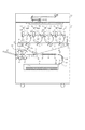
図1は、本発明の画像形成装置の一実施例に係る電子写真カラー複写機の全体構成を示す概略断面図である。本実施例の電子写真カラー複写機は、複数の画像形成部を並列に配し、且つ中間転写方式を採用したカラー画像形成装置である。 FIG. 1 is a schematic sectional view showing the overall configuration of an electrophotographic color copying machine according to an embodiment of an image forming apparatus of the present invention. The electrophotographic color copying machine of this embodiment is a color image forming apparatus in which a plurality of image forming units are arranged in parallel and an intermediate transfer method is adopted.
本実施形態における画像形成装置は、画像読取部1Rと、画像出力部1Pとを有する。画像読取部1Rは、原稿画像を光学的に読み取り、電気信号に変換して画像出力部1Pに送信する。画像出力部1Pは、画像形成部10(10a、10b、10c、10d)と、給紙ユニット20と、中間転写ユニット30と、定着ユニット40と、クリーニングユニット50、70と、フォトセンサ60と、制御ユニット80とを有する。
The image forming apparatus according to the present embodiment includes an image reading unit 1R and an image output unit 1P. The image reading unit 1R optically reads a document image, converts it into an electrical signal, and transmits it to the image output unit 1P. The image output unit 1P includes an image forming unit 10 (10a, 10b, 10c, 10d), a paper feeding unit 20, an intermediate transfer unit 30, a
更に、個々のユニットについて詳しく説明する。 Further, each unit will be described in detail.
画像形成部10a〜10dはそれぞれ同じ構成を有し、イエロー、マゼンタ、シアン、ブラックの各色毎のトナー像を形成する。図1において、数字及びTの添え字a,b,c,dはそれぞれイエロー、マゼンタ、シアン、ブラックの画像形成部の構成であることを示す。それぞれの画像形成部の構成は同じであるので、添え字a〜dを省略して1つの画像形成部で説明する。 Each of the image forming units 10a to 10d has the same configuration, and forms a toner image for each color of yellow, magenta, cyan, and black. In FIG. 1, numerals and T suffixes a, b, c, and d indicate the configurations of the image forming units of yellow, magenta, cyan, and black, respectively. Since the configuration of each image forming unit is the same, the subscripts a to d are omitted, and description will be made with one image forming unit.
画像形成部10では、第一の像担持体としてのドラム状の感光体11が回転自在に軸支され、矢印方向に回転駆動される。感光体11の外周面に対向してその回転方向に一次帯電器12、光学系13、折り返しミラー16、現像装置14、及びクリーニング装置15が配置されている。
In the
一次帯電器12において感光体ドラム11の表面に均一な帯電量の電荷を与える。次いで、光学系13により、画像読取部1Rからの記録画像信号に応じて変調した、例えばレーザビームなどの光線を折り返しミラー16を介して感光体ドラム11上に露光することによって、そこに静電潜像を形成する。
The
更に、現像剤(以下、「トナー」という)を収納した現像装置14によって上記静電潜像を顕像化する。なお、現像器14a〜14dには、それぞれイエロー、マゼンタ、シアン、ブラックのトナーが収納されている。 Further, the electrostatic latent image is visualized by a developing device 14 containing a developer (hereinafter referred to as “toner”). The developing devices 14a to 14d store yellow, magenta, cyan, and black toners, respectively.
画像形成部10a〜10dでそれぞれ顕像化された可視画像は画像転写領域Tにて中間転写ユニット30を構成する第二の像担持体としてのベルト状の中間転写体、即ち、中間転写ベルト31に重ねて転写される。中間転写ユニット30については、後で詳述する。
The visible images respectively visualized by the image forming units 10a to 10d are belt-shaped intermediate transfer members as a second image carrier constituting the intermediate transfer unit 30 in the image transfer region T, that is, the
画像転写領域Tの下流側では、クリーニング装置15により中間転写体に転写されずに感光体ドラム11上に残されたトナーを掻き落として感光体ドラム11の表面の清掃を行う。以上に示したプロセスにより、各トナーによる画像形成が順次行われる。
On the downstream side of the image transfer region T, the
給紙ユニット20は、転写材Pを収納するためのカセット21と、カセット21より転写材Pを一枚ずつ送り出すためのピックアップローラ22と、ピックアップローラ22sで送り出された転写材Pを更に搬送するための給紙ローラ対23を有する。給紙ユニット20は更に、給紙ガイド24と、そして、各画像形成部の画像形成タイミングに合わせて転写材Pを二次転写領域Teへ送り出すためのレジストレーションローラ25とを有する。
The paper feeding unit 20 further conveys the cassette 21 for storing the transfer material P, the pickup roller 22 for feeding the transfer material P one by one from the cassette 21, and the transfer material P sent out by the pickup roller 22s. A pair of
中間転写ユニット30について詳細に説明する。 The intermediate transfer unit 30 will be described in detail.
中間転写ベルト31は、中間転写ベルト31に駆動を伝達する駆動ローラ32と、中間転写ベルト31の回動に従動する従動ローラ33と、二次転写対向ローラ34とに巻き回されている。又、駆動ローラ32と従動ローラ33の間に一次転写平面Aが形成される。中間転写ベルト31としては、例えばPET(ポリエチレンテレフタレート)、PVdF(ポリフッ化ビニリデン)などが用いられる。駆動ローラ32は、金属ローラの表面に数mm厚のゴム(ウレタン又はクロロプレン)をコーティングしてベルトとのスリップを防いでいる。駆動ローラ32は、パルスモータ(不図示)によって回転駆動される。
The
各感光体ドラム11a〜11dと中間転写ベルト31が対向する一次転写領域Ta〜Tdには、中間転写ベルト31の裏に一次転写用帯電器35(35a〜35d)が配置されている。一方、二次転写対向ローラ34に対向して二次転写ローラ36が配置され、中間転写ベルト31とのニップによって二次転写領域Teを形成する。二次転写ローラ36は、中間転写ベルト31に対して適度な圧力で加圧されている。
Primary transfer chargers 35 (35 a to 35 d) are disposed on the back of the
また、中間転写ベルト31の二次転写領域Teの下流には中間転写ベルト31の画像形成面をクリーニングするためのクリーニングユニット50が配置される。クリーニングユニット50は、中間転写ベルト31上のトナーを除去するためのクリーニングブレード51と、転写されなかったトナーを収納する廃トナーボックス52とを備えている。
A
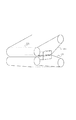
定着ユニット40は、加熱手段としての電磁誘導加熱用のIHコイルの駆動回路211などを備えた定着ベルト41aと、そのベルト加圧される加圧ベルト41b(このベルトにも熱源を備える場合もある)とを有する。定着ベルト41aと加圧ベルト41bは不図示の圧解除ユニットにより離間することが可能である。
The fixing
また、定着ユニット40から排出されてきた転写材Pをさらに装置外部に導き出すための内排紙ローラ27、外排紙ローラ28及び転写材P積載する排紙トレイ29が設けられている。
Further, an internal
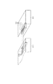
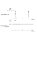
なお、定着ユニット40は、画像形成装置本体に対して着脱可能なユニットであり、本体とはドロアコネクタに代表される着脱可能なコネクタで電気的に接続されている。図2に着脱可能なコネクタの例を示す。
The fixing
図2において、1001は画像形成装置本体側に設けられたコネクタ、1002は定着ユニット40側に設けられたコネクタである。コネクタ1001とコネクタ1002には、それぞれ接触子1003と1004が備えられ、コネクタ1001とコネクタ1002が接合すると、接触子1003と1004が嵌合して電気的に導通がなされる。
In FIG. 2, 1001 is a connector provided on the image forming apparatus main body side, and 1002 is a connector provided on the fixing
なお、接触子1003および1004は、コネクタを互いに嵌合または結合させない状態で大気中の放置しておくと、コネクタピンのメッキの状態によっては、その表面に酸化皮膜が形成されてしまうことがある。
In addition, if the
そして、コネクタピンに酸化皮膜が形成された場合、コネクタを互いに嵌合させて通電させても、電流値が低い場合は酸化皮膜を破壊できず、電気的接続が得られないことがある。 When an oxide film is formed on the connector pins, even if the connectors are fitted to each other and energized, the oxide film cannot be broken and the electrical connection may not be obtained if the current value is low.
図3に示すように、定着ユニット40内には、定着ベルトの温度を検出するための温度センサ202が配置されている。また温度センサ202の素子としてはサーミスタを用いている。
As shown in FIG. 3, a
温度センサ202にてベルト表面の温度が検出され、予め設定された目標温度となるように、IHコイル駆動回路211への供給電力が制御される。
The temperature of the belt surface is detected by the
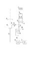
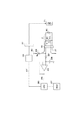
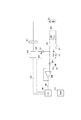
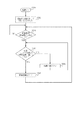
図4は、定着ユニット40の温度制御のための回路構成を示すブロック図である。
FIG. 4 is a block diagram showing a circuit configuration for temperature control of the fixing
201はコネクタであり、図2に示したコネクタ1001と1002とが嵌合している状態を示している。図4において、コネクタ201の右側が定着ユニット40側の回路であり、コネクタ201の左側が画像形成装置本体側の回路である。203は電源、204はサーミスタ202に流れる電流を設定するための電流設定抵抗、207及び208はノイズ除去フィルタを構成する抵抗とコンデンサである。206はサーミスタ202の出力をバッファするオペアンプ、209は、定着装置の温度制御を行うCPUである。211は定着器を電磁誘導方式により加熱するためのコイル、220はコイル212の駆動回路である。コイル駆動回路2202は、不図示の商用交流電源が接続され、コイル211へ供給される電力を制御する。CPU209は、サーミスタ202のからの検知信号205に基づいて温度を求め、検出した温度が所定温度となるように、コイル211に供給する電力を制御するための加熱制御信号212をコイル駆動回路220へ出力している。221はコイル211と交流電源とを接続するコネクタである。なお、コネクタ221には、8アンペア程度の大きな電流が流れるため、仮に酸化皮膜が形成されたとしても、コイル211を駆動する電流によって破壊される。301はコネクタ201を流れる電流の値を所定値以上にするための抵抗である。詳しくは後述する。
以下にサーミスタによる温度検出方法について詳述する。 The temperature detection method using the thermistor will be described in detail below.
サーミスタ202への電源供給は、コネクタ部201に対してサーミスタ202と反対側に設けられた電源203からコネクタ部201を介してより行われている。サーミスタ202へ供給する電流値は、電源203の電圧値Vと電流設定抵抗204の抵抗値Raにより決定される。サーミスタ202は、温度Tに対して抵抗値Rthが変化する特性を持つデバイスである。図5にサーミスタ202の特性を示す。サーミスタ202の検出電圧(Vdet)は、以下の式で決定される。
Vdet=(V/(Ra+Rth))×Rth
例えば、V=3.3V、Ra=2kΩ、T=220℃の場合、図5の特性に従うとRth=0.368kΩなので、Vdet=0.517Vとなる。検出電圧Vdetは、ノイズ除去フィルタである抵抗207とコンデンサ208を通ったあと、オペアンプ206によりバッファされ、CPU209のA/Dコンバータに入力される。
Power is supplied to the
Vdet = (V / (Ra + Rth)) × Rth
For example, when V = 3.3 V, Ra = 2 kΩ, and T = 220 ° C., Rth = 0.368 kΩ according to the characteristics shown in FIG. 5, so Vdet = 0.517V. The detection voltage Vdet passes through a
上記の計算式より、検出電圧Vdetに対する温度Tが決定される。バックアップされたRAM210には、図6に示す温度と検出電圧の対応を示すテーブルが格納されており、CPU209のA/Dコンバータの分解能が8bitであれば、CPU209は検出電圧Vdetを図6のようなHEX値で読み取ることが出来る。CPU209は読み取った検出電圧から対応する温度Tを求めることが出来る。
The temperature T with respect to the detection voltage Vdet is determined from the above calculation formula. 6 is stored in the backed-up
次に、上記構成の電子写真カラー複写機の動作について説明する。 Next, the operation of the electrophotographic color copying machine having the above configuration will be described.
CPU209により画像形成動作の開始信号が発せられると、ピックアップローラ22aにより、カセット21aから転写材Pが一枚ずつ送り出される。そして、給紙ローラ対23によって転写材Pが給紙ガイド24の間を案内されてレジストレーションローラ25まで搬送される。その時、レジストレーションローラ25の駆動は停止されており、転写材Pの先端はレジストレーションローラ25のニップ部に突き当たる。その後、画像形成部が画像の形成を開始するタイミングに合わせてレジストレーションローラ25は回転を始める。この回転時期は、転写材Pと画像形成部より中間転写ベルト31上に一次転写されたトナー画像とが二次転写領域Teにおいて一致するようにそのタイミングが設定されている。
When the
一方、画像形成部では、画像形成動作開始信号が発せられると、前述したプロセスにより感光体ドラム11d上に形成されたトナー画像が、高電圧が印加された一次転写用帯電器35dによって一次転写領域Tdにおいて中間転写ベルト31に一次転写される。一次転写されたトナー像は次の一次転写領域Tcまで搬送される。そこでは各画像形成部間をトナー像が搬送される時間だけ遅延して画像形成が行われており、既に転写されているトナー画像に重ねてその次のトナー像が転写される。以下も同様の工程が繰り返され、結局4色のトナー像が中間転写ベルト31上において転写される。
On the other hand, in the image forming section, when an image forming operation start signal is issued, the toner image formed on the photosensitive drum 11d by the above-described process is transferred to the primary transfer region by the
その後、転写材Pが二次転写領域Teに進入し、中間転写ベルト31に到達すると、転写材Pの通過タイミングに合わせて二次転写ローラ36に高電圧を印加する。これにより、前述したプロセスにより中間転写ベルト31上に形成された4色のトナー画像が転写材Pの表面に転写される。その後、転写材Pは搬送ガイド43によって定着ユニット40へ搬送される。そして、ベルト41a、41bの熱及びニップの圧力によってトナー画像が転写材Pの表面に定着される。その後、転写材Pは内排紙ローラ27、外排紙ローラ28により搬送され、転写材Pは機外に排出され、排紙トレイ29に積載される。
Thereafter, when the transfer material P enters the secondary transfer region Te and reaches the
次に本発明の特徴となる定着ユニット40と本体を接続する信号線およびコネクタ部の導通状態を安定させる構成について、図4、図7を用いて説明する。
Next, a configuration for stabilizing the conduction state of the signal line and the connector portion connecting the fixing
図4において、抵抗体301は、コネクタ部201に対してサーミスタ202と同じ側に配置され、かつサーミスタ202の両端と並列に接続される。図7は、図4において、サーミスタ202と抵抗体301に夫々流れる電流経路を付加した図である。サーミスタ202は特に低温環境においては抵抗値が高いために、コネクタ部201からサーミスタ202までの信号線(図7のAに示す経路)上に流れる電流値が微少である。従って、低温環境では、サーミスタ202からの検知信号が外乱ノイズを受けやすくなったり、コネクタ部201の端子において酸化皮膜が形成された場合に、その酸化皮膜を破壊できずに接触不良になることがある。また、コネクタ部201を含む信号線上の電流を増加させるだけでは、サーミスタの自己発熱が大きくなり、定着温度の検出結果にズレが生ずる。
In FIG. 4, the
そこで図12に示す従来の回路に抵抗体301を追加することによって、図7のBに示す電流経路の電流値を増加させるようにしている。具体的には、サーミスタ202の抵抗値に関わらずに、コネクタ部201および信号線上に一定以上の電流が流れるように抵抗体301を設ける。即ち、抵抗体301はコネクタ部201に対してサーミスタ202側に設けることによってコネクタ部201に流れる電流を増加させることができる。その結果、サーミスタ202からの検出信号が外乱ノイズに対して耐性が向上し、更に、コネクタ部201に酸化皮膜が発生した場合において酸化皮膜を溶融破壊させうる電流を流すことができる。
Therefore, by adding a
一方、抵抗体301をコネクタ部201に対してサーミスタ202と逆側(CPU209等の制御ユニット側)に設けた場合には、図7のBに示した電流経路を形成することができないので、コネクタ201に流れる電流を増加させることができない。
On the other hand, when the
なお、コネクタ部201およびサーミスタ202への信号線に流れる電流値は、サーミスタ202からの検出信号が信号線上における外乱ノイズの影響を受けない大きさ、かつコネクタ部201の端子の酸化皮膜を溶融破壊できる十分な電流値であれば良い。また、抵抗体301の抵抗値は、抵抗体301に流れる電流がサーミスタ202に流れる電流よりも大きくなるような抵抗値に設定される。
The value of the current flowing in the signal line to the
本実施形態においては、その電流値を1.0mA以上としている。コネクタ部201およびサーミスタ202への信号線に流れる電流値を1.0mA以上にするために、抵抗体301の抵抗値を2.4kΩとし、かつ電流設定抵抗204の抵抗値も2.4kΩに設定する。また、電源203の電圧値を5Vに設定している。上記の値に設定することで、コネクタ部201および信号線上に流れる電流値、サーミスタ202の抵抗値、サーミスタ202と抵抗体301の合成抵抗値、検知温度の関係は図8の如くとなる。
In the present embodiment, the current value is 1.0 mA or more. The resistance value of the
例えばサーミスタの検知温度が20℃の場合の合成抵抗値は、サーミスタ202の抵抗値が43.907kΩであるので、合成抵抗値は
1/{(1/43.907kΩ)+(1/2.4kΩ)}=2.276kΩ
となる。このときの電流値は、
5V/(2.276kΩ+2.4kΩ)=1.069mA
となる。
For example, when the thermistor detection temperature is 20 ° C., the combined resistance value is 43.907 kΩ, and the combined resistance value is 1 / {(1 / 43.907 kΩ) + (1 / 2.4 kΩ). )} = 2.276kΩ
It becomes. The current value at this time is
5V / (2.276 kΩ + 2.4 kΩ) = 1.068 mA
It becomes.
図9は、図4および図7に示した回路におけるサーミスタ202と抵抗体301の合成抵抗値、サーミスタ202の検知電圧(検知信号205の電圧)及びCPU209のA/Dコンバータのデジタル値の関係を表す。
9 shows the relationship between the combined resistance value of the
検出電圧(Vdet)は、以下のようにして決定される。
Vdet=(V/(Ra+合成抵抗値))×合成抵抗値
例えば検知温度20℃の場合、上述の如く合成抵抗値=2.276kΩであり、また電源203の電圧値V=5V、電流設定抵抗204の抵抗値Ra=2.4kΩであるので、
Vdet=(5/(2.4+2.276))×2.276=2.433Vとなる。
The detection voltage (Vdet) is determined as follows.
Vdet = (V / (Ra + combined resistance value)) × combined resistance value For example, when the detection temperature is 20 ° C., the combined resistance value = 2.276 kΩ as described above, the voltage value V = 5 V of the
Vdet = (5 / (2.4 + 2.276)) × 2.276 = 2.433V.
また検知電圧VdetとAD入力値との関係は、CPU209のA/Dコンバータが8bit分解能であれば、図9に示す値となる。従って、図9に示すテーブルをRAM210に格納しておくことで、読み取った検出電圧から定着ユニット40の温度を求めることができる。
The relationship between the detection voltage Vdet and the AD input value is the value shown in FIG. 9 if the A / D converter of the
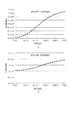
図10(1)は、図12に示す抵抗体301が設けられていない従来の構成における検知温度と信号線の電流との関係を示すグラフ、図10(2)は本実施形態における検知温度と信号線の電流との関係を示すグラフである。図10(1)に示すように、従来構成では、検知温度が20℃の場合のコネクタ部201および信号線上に流れる電流値は、0.1mA(100μA)程度である。これに対して本実施形態の構成では、抵抗体301を追加することによって、抵抗体301を介して流れる電流が加算されるため、20℃の環境でも1.0mA以上を確保することが可能である。
FIG. 10A is a graph showing the relationship between the detected temperature and the signal line current in the conventional configuration in which the
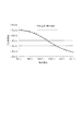
図11に、検知電圧と検知温度との関係のグラフを示す。 FIG. 11 shows a graph of the relationship between the detected voltage and the detected temperature.
なお電源203および電流設定抵抗204の値は、CPU209のA/Dコンバータ部における分解能を考慮して設定すれば良い。またコネクタ201に流れる電流の目標値は、サーミスタ202に電流が流れることによってサーミスタ自身の温度上昇が許容範囲内に収まるように設定するのが好ましい。本実施形態においては、サーミスタ202の温度上昇値を1℃以下(制御温度220℃付近)にすることを考慮している。以上を考慮して本実施形態では、電源203の電圧値を5V、電流設定抵抗204および抵抗体301の抵抗値を2.4kΩに設定しているが、もちろんこの値に限定されるものではなく、装置に合わせて最適に設定するのが良い。
The values of the
即ち、
・サーミスタ202の信号線上における外乱ノイズの影響を受けない電流値、且つ、コネクタ部201の端子上に酸化皮膜が発生してしまった場合に、酸化皮膜を溶融破壊するために十分な電流値。
・検知電圧の分解能。
・サーミスタ自身の温度上昇。
That is,
A current value that is not affected by disturbance noise on the signal line of the
・ Resolution of detection voltage.
・ Thermistor's own temperature rise.
以上の点に鑑みて、抵抗体301の値および、さらに必要に応じて電圧203の電圧値や、電流設定抵抗204の値を決定すればよい。
In view of the above points, the value of the
以上のように、定着ユニット40が低温状態であり、サーミスタに微少電流しか流れない状態においても、サーミスタ自身の温度上昇を抑えながらサーミスタの信号経路におけるコネクタ部や信号線上の電流値を増加させることができる。これにより、サーミスタの信号線上における外乱ノイズの耐性向上および、コネクタ部における導通状態を改善させることにより、安定した温度検知を可能にすることができる。
As described above, even when the fixing
抵抗体301の値はもちろんこれに限定されるものではなく、コネクタ部201の端子等の仕様やサーミスタの信号線の状況に応じて設定すれば良い。
Of course, the value of the
(第2の実施の形態)
図13は第2の実施の形態における温度制御回路である。図4の回路同じ構成要素に関しては同じ符号を付し、詳細な説明を省略する。
(Second Embodiment)
FIG. 13 shows a temperature control circuit according to the second embodiment. The same components as those in the circuit of FIG. 4 are denoted by the same reference numerals, and detailed description thereof is omitted.
図4の回路との違いは、抵抗体301の代わりに、コンデンサ401が設けられている点と、電圧印加部402及び、電圧印加部402から一瞬パルス状の波形の電圧を発生させ印加信号403が設けられている点である。電圧印加部402は印加信号403により、コネクタ201からコンデンサ401への電流径路上に図15に示すようなパルス状の電流を重畳する。印加信号403は画像形成装置の電源投入や画像形成開始の指示の入力、コネクタ201の接続などに応じてCPU209から出力されるが、任意のタイミングでCPU209が発生しても良い。
4 differs from the circuit of FIG. 4 in that a
コンデンサ401はコネクタ部201に対して、サーミスタ202と同じ側に設けられ、電圧印加部402はコネクタ部201に対してサーミスタ202とは反対側に設けられる。電圧印加部402からのパルス状の電圧が発生され、コネクタ部201に流れる電流にパルス状の電流が重畳されることにより、コネクタ部201に流れる電流を増加させる。
The
図14は、図13の回路において、電流経路を示した図である。低温環境においてはサーミスタ202の抵抗値が高いために、コネクタ部201およびコネクタ部201を介してサーミスタ202までの信号線(図14のAに示す経路)上に流れる電流値が微少である。その場合には前述したように、コネクタ部201の端子において酸化皮膜が形成された場合に、コネクタ部201に電流が流れても、その酸化皮膜を破壊できずに接触不良に至ることがある。
FIG. 14 is a diagram showing current paths in the circuit of FIG. Since the resistance value of the
そこで、コンデンサ401及び電圧印加部402とを追加することによって、図14のBに示す電流経路によりコネクタ部201に流れる電流値を増加させるようにしている。
Therefore, by adding the
図15は、電圧印加部402が出力するパルス状の電流と、該パルス状の電流を印加した際のサーミスタ202の検出信号205を示す波形図である。このパルス状の電流の値および印加時間は、コネクタ部201の端子上に酸化皮膜が発生してしまった場合に、酸化皮膜を溶融破壊するために十分な電流値と印加時間に設定すれば良い。また、コンデンサ401の容量は、コンデンサ401に流れる電流のピーク値がサーミスタ202に流れる直流の電流よりも大きくなるような容量に設定される。本実施形態においては、パルス状の電流の値Iを100mA、印加時間Tを0.1μsとしている。電流値および印加時間はもちろんこの値に限定されるものではなく、コネクタ部201の端子等の仕様に合わせて適切に設定すれば良い。
FIG. 15 is a waveform diagram showing a pulsed current output from the
そしてコンデンサ401は、電圧印加部402にて重畳したパルス状の電流を通過させうる大きさの容量、かつ温度検出において要求される応答性を満たすように容量を設定すれば良い。例えば本実施形態ではコンデンサ401の容量を22μFとしている。もちろんコンデンサ401もこの値に限定されるものでは無い。
上記の構成により、サーミスタ202の検知信号経路は、図15に示すように、電圧印加部402からのパルス電流の重畳の有無に関わらずに、CPU209は直流的に安定した信号として検知することが可能となる。従って、CPU209は定着ユニット40を精度良く目標温度に制御することが可能である。
With the above configuration, the detection signal path of the
次に本実施形態におけるCPU209の制御シーケンスについて、図16を用いて説明する。図16はCPU209が実行する定着ユニットの温度制御のフローチャートである。
Next, a control sequence of the
画像形成装置の電源が投入される(ステップS501)と、CPU209は電圧印加部402に対して印加信号403を出力する(ステップS502)。電圧印加部402は印加信号403に基づいてサーミスタ202の電流経路上にパルス状の電流を重畳させる。この時に、コネクタ部201に流れる電流が増加するため、コネクタ部201に酸化皮膜が形成されていたとしても、電流によりその酸化皮膜が破壊されて、サーミスタ202からの信号の導通状態が改善される。なお前述のように、CPU209が電圧印加部402に対して印加信号403を出力するタイミングは電源オン時に限定されるものではない。
When the image forming apparatus is turned on (step S501), the
続いてCPU209は、画像形成開始の指示が入力されたか否かを判断する(ステップS503)。画像形成開始の指示がない場合は、CPU209は、定着ユニット40内の駆動回路211をオフさせた状態まま、指示を待つことになる。画像形成開始の指示が入力された場合、CPU209は、定着ユニット40の温度が目標温度に達しているか否かを判断する(ステップS504)。そして、定着ユニット40の温度が目標温度に達していれば、CPU209は定着ユニット内の駆動回路211をオフさせたまま(ステップS505)、再びステップS503へ戻る。定着ユニット40の温度が目標温度に達していない場合は、定着ユニット40内の駆動回路211を駆動させ、誘導加熱により定着ユニット40を加熱させ(ステップS506)、再びステップS504に戻る。なお、本実施形態では、電磁誘導加熱方式の定着ユニットを用いているため、像形成開始の指示が入力されてから定着ユニット40の過熱を開始しているが、ハロゲンヒータを用いた定着ユニットであれば、電源オン後に加熱を開始する。
Subsequently, the
以上説明したようにして、定着ユニット40が低温状態であってサーミスタ202に微少電流しか流れない状態においても、サーミスタ202自身の温度上昇を抑えながらコネクタ部201や信号線上の電流値を増加させることができる。これにより、コネクタ部201における導通状態を改善させることにより、安定した温度検知及び温度制御を可能にすることができる。
As described above, even when the fixing
201 コネクタ部
202 サーミスタ
203 電源
204 電流設定抵抗
205 サーミスタからの検知信号
209 CPU
210 RAM
301 抵抗体
401 コンデンサ
402 電圧印加部
201
210 RAM
Claims (5)
温度が低いほど抵抗値が高くなる素子を有し、前記定着ユニットの温度を検出する温度センサと、
前記温度センサからの信号を伝達するためのコネクタと、
前記コネクタに対して前記温度センサとは反対側に接続され、前記温度センサからの信号に基づいて前記定着ユニットの温度を制御する制御部と、
前記コネクタに対して前記温度センサと同じ側で、前記温度センサと並列に接続される抵抗体と、
前記コネクタに対して前記温度センサとは反対側に設けられ、前記コネクタを介して前記温度センサ及び前記抵抗体に電流を流すための電源と、
を有することを特徴とする画像形成装置。 In an image forming apparatus comprising: an image forming unit that forms a toner image on a transfer material; and a fixing unit that fixes the toner image formed on the transfer material.
A temperature sensor that has an element whose resistance value increases as the temperature decreases, and detects the temperature of the fixing unit;
A connector for transmitting a signal from the temperature sensor;
A controller that is connected to the connector on the opposite side of the temperature sensor and controls the temperature of the fixing unit based on a signal from the temperature sensor;
A resistor connected in parallel with the temperature sensor on the same side as the temperature sensor with respect to the connector;
A power supply for passing a current to the temperature sensor and the resistor through the connector;
An image forming apparatus comprising:
温度が低いほど抵抗値が高くなる素子を有し、前記定着ユニットの温度を検出する温度センサと、
前記温度センサからの信号を伝達するためのコネクタと、
前記コネクタに対して前記温度センサとは反対側に接続され、前記温度センサからの信号に基づいて前記定着ユニットの温度を制御する制御部と、
前記コネクタに対して前記温度センサと同じ側で、前記温度センサと並列に接続されるコンデンサと、
前記コネクタに対して前記温度センサとは反対側に設けられ、前記コネクタを介して前記温度センサに電流を流すための電源と、
前記コネクタに対して前記制御部と同じ側に設けられ、前記コネクタを介して前記コンデンサにパルス状の電流を流すための電圧を発生する電圧印加部と、
を有し、前記制御部は前記画像形成装置の電源投入に応じて前記電圧印加部に対して前記パルス状の電流を流すための信号を出力することを特徴とする画像形成装置。 In an image forming apparatus comprising: an image forming unit that forms a toner image on a transfer material; and a fixing unit that fixes the toner image formed on the transfer material.
A temperature sensor that has an element whose resistance value increases as the temperature decreases, and detects the temperature of the fixing unit;
A connector for transmitting a signal from the temperature sensor;
A controller that is connected to the connector on the opposite side of the temperature sensor and controls the temperature of the fixing unit based on a signal from the temperature sensor;
A capacitor connected in parallel with the temperature sensor on the same side as the temperature sensor with respect to the connector;
A power source provided on the opposite side of the temperature sensor with respect to the connector, and for passing a current to the temperature sensor via the connector;
A voltage applying unit that is provided on the same side as the control unit with respect to the connector and generates a voltage for flowing a pulsed current to the capacitor via the connector;
And the control unit outputs a signal for causing the pulsed current to flow to the voltage application unit in response to power-on of the image forming apparatus.
Priority Applications (2)
| Application Number | Priority Date | Filing Date | Title |
|---|---|---|---|
| JP2008150487A JP2009294167A (en) | 2008-06-09 | 2008-06-09 | Image forming apparatus |
| US12/480,401 US8385764B2 (en) | 2008-06-09 | 2009-06-08 | Image forming apparatus |
Applications Claiming Priority (1)
| Application Number | Priority Date | Filing Date | Title |
|---|---|---|---|
| JP2008150487A JP2009294167A (en) | 2008-06-09 | 2008-06-09 | Image forming apparatus |
Publications (2)
| Publication Number | Publication Date |
|---|---|
| JP2009294167A true JP2009294167A (en) | 2009-12-17 |
| JP2009294167A5 JP2009294167A5 (en) | 2011-07-28 |
Family
ID=41400433
Family Applications (1)
| Application Number | Title | Priority Date | Filing Date |
|---|---|---|---|
| JP2008150487A Withdrawn JP2009294167A (en) | 2008-06-09 | 2008-06-09 | Image forming apparatus |
Country Status (2)
| Country | Link |
|---|---|
| US (1) | US8385764B2 (en) |
| JP (1) | JP2009294167A (en) |
Cited By (1)
| Publication number | Priority date | Publication date | Assignee | Title |
|---|---|---|---|---|
| JP7512595B2 (en) | 2020-01-16 | 2024-07-09 | 株式会社リコー | Fixing device and image forming apparatus |
Families Citing this family (3)
| Publication number | Priority date | Publication date | Assignee | Title |
|---|---|---|---|---|
| JP5982413B2 (en) * | 2014-02-20 | 2016-08-31 | 京セラドキュメントソリューションズ株式会社 | Post-processing apparatus, image forming apparatus, and image forming system |
| JP6204329B2 (en) * | 2014-11-28 | 2017-09-27 | 京セラドキュメントソリューションズ株式会社 | Fixing apparatus and image forming apparatus |
| JP2020122820A (en) * | 2019-01-29 | 2020-08-13 | 株式会社リコー | Fixing device and image forming apparatus |
Family Cites Families (5)
| Publication number | Priority date | Publication date | Assignee | Title |
|---|---|---|---|---|
| JPH04190382A (en) * | 1990-11-26 | 1992-07-08 | Fujitsu Ltd | Detecting and protecting circuit for toner fixing unit |
| JPH0835860A (en) | 1994-07-22 | 1996-02-06 | Mitsubishi Electric Corp | Sensor control device |
| JP3265843B2 (en) | 1994-08-04 | 2002-03-18 | 株式会社デンソー | Connector pin connection device and method of assembling the same |
| US5971935A (en) * | 1998-05-01 | 1999-10-26 | Baxter International Inc. | Methods and apparatus for reducing noise in systems using thermistor catheters to measure biological functions |
| US6420854B1 (en) * | 2001-05-17 | 2002-07-16 | Hubbell Incorporated | Battery detector |
-
2008
- 2008-06-09 JP JP2008150487A patent/JP2009294167A/en not_active Withdrawn
-
2009
- 2009-06-08 US US12/480,401 patent/US8385764B2/en not_active Expired - Fee Related
Cited By (1)
| Publication number | Priority date | Publication date | Assignee | Title |
|---|---|---|---|---|
| JP7512595B2 (en) | 2020-01-16 | 2024-07-09 | 株式会社リコー | Fixing device and image forming apparatus |
Also Published As
| Publication number | Publication date |
|---|---|
| US20090304405A1 (en) | 2009-12-10 |
| US8385764B2 (en) | 2013-02-26 |
Similar Documents
| Publication | Publication Date | Title |
|---|---|---|
| US9081340B2 (en) | Image forming apparatus having first and second cooling portions or fans cooling end regions of a fixing portion with respect to a direction perpendicular to a recording material conveyance direction | |
| US9501003B2 (en) | Image forming apparatus | |
| JP5825298B2 (en) | Image forming apparatus | |
| US10416595B2 (en) | Image forming apparatus having a control circuit that selectively controls power to be supplied to a plurality of heat generating blocks of a heater | |
| JP7301677B2 (en) | image forming device | |
| CN101021710A (en) | Fixing device | |
| JP5089146B2 (en) | Image heating apparatus and image forming apparatus | |
| US10990054B2 (en) | Image forming apparatus that corrects a target temperature for heating a region without a toner image when an abnormality is detected | |
| JP4931664B2 (en) | Image forming apparatus | |
| US8649698B2 (en) | Image forming apparatus controlling power to a heating unit forming a fixing nip portion with a pressure roller through which a recording sheet is conveyed to fix a toner image thereon | |
| JP2010054688A (en) | Temperature control device and control method | |
| JP2009294167A (en) | Image forming apparatus | |
| JP5460442B2 (en) | Power supply control device and image forming apparatus | |
| JP5406951B2 (en) | Power supply control apparatus, electronic device, and image forming apparatus | |
| JP2007035606A (en) | Heating device, fixing device and image forming apparatus | |
| JP6187224B2 (en) | Image forming apparatus | |
| JP2009025365A (en) | Image heating heater and image heating apparatus | |
| JP5329032B2 (en) | Image forming apparatus | |
| JP2012226048A (en) | Image forming apparatus | |
| JP2011033808A (en) | Image forming apparatus | |
| JP2013195470A (en) | Power supply unit, image forming apparatus, and output error detection method | |
| US10191437B2 (en) | Image forming apparatus, method of controlling image forming apparatus, and non-transitory computer readable medium storing program for method of controlling image forming apparatus | |
| JP5862626B2 (en) | Fixing apparatus and image forming apparatus | |
| JP2021096427A (en) | Image forming apparatus | |
| US12554218B2 (en) | Temperature control device and image forming apparatus including temperature control device |
Legal Events
| Date | Code | Title | Description |
|---|---|---|---|
| RD04 | Notification of resignation of power of attorney |
Free format text: JAPANESE INTERMEDIATE CODE: A7424 Effective date: 20100201 |
|
| RD01 | Notification of change of attorney |
Free format text: JAPANESE INTERMEDIATE CODE: A7421 Effective date: 20100630 |
|
| A521 | Request for written amendment filed |
Free format text: JAPANESE INTERMEDIATE CODE: A523 Effective date: 20110608 |
|
| A621 | Written request for application examination |
Free format text: JAPANESE INTERMEDIATE CODE: A621 Effective date: 20110608 |
|
| A761 | Written withdrawal of application |
Free format text: JAPANESE INTERMEDIATE CODE: A761 Effective date: 20120127 |