JP2009277686A - Method of forming insulating film, and insulating film - Google Patents
Method of forming insulating film, and insulating film Download PDFInfo
- Publication number
- JP2009277686A JP2009277686A JP2008124604A JP2008124604A JP2009277686A JP 2009277686 A JP2009277686 A JP 2009277686A JP 2008124604 A JP2008124604 A JP 2008124604A JP 2008124604 A JP2008124604 A JP 2008124604A JP 2009277686 A JP2009277686 A JP 2009277686A
- Authority
- JP
- Japan
- Prior art keywords
- insulating film
- dielectric constant
- forming
- film
- air atmosphere
- Prior art date
- Legal status (The legal status is an assumption and is not a legal conclusion. Google has not performed a legal analysis and makes no representation as to the accuracy of the status listed.)
- Pending
Links
Images
Abstract
Description
この発明は、半導体装置の層間絶縁膜などに有用な絶縁膜を成膜する際に用いられる絶縁膜およびこれの成膜方法に関し、低誘電率で、かつ高機械的強度および高安定性を有する絶縁膜が得られるようにしたものである。 The present invention relates to an insulating film used when forming an insulating film useful as an interlayer insulating film of a semiconductor device and a film forming method thereof, and has a low dielectric constant, high mechanical strength, and high stability. An insulating film is obtained.
半導体装置の高集積化に伴い、配線層が微細化されつつある。しかし、微細な配線層では、配線層における信号遅延の影響が大きくなり、信号伝送速度の高速化を妨げている。 この信号遅延は、配線層の抵抗と配線層間容量に比例するため、高速化を実現するためには、配線層の低抵抗化と配線層間容量の低減が必須である。 As semiconductor devices are highly integrated, wiring layers are being miniaturized. However, in the fine wiring layer, the influence of the signal delay in the wiring layer is increased, which hinders the increase in the signal transmission speed. Since this signal delay is proportional to the resistance of the wiring layer and the wiring interlayer capacitance, it is essential to reduce the resistance of the wiring layer and reduce the wiring interlayer capacitance in order to achieve high speed.
このため、最近では配線層を構成する材料として、従来のアルミニウムから抵抗率の低い銅が用いられ、さらに配線層間容量を減らすために比誘電率の低い層間絶縁膜が用いられている。
例えば、SiO2膜が4.1、SiOF膜が3.7の比誘電率を有するが、さらに比誘電率の低いSiOCH膜や有機膜を用いるようになっている。
Therefore, recently, copper having a lower resistivity than conventional aluminum is used as a material constituting the wiring layer, and an interlayer insulating film having a low relative dielectric constant is further used to reduce the wiring interlayer capacitance.
For example, the SiO 2 film has a relative dielectric constant of 4.1 and the SiOF film has a relative dielectric constant of 3.7, but an SiOCH film or an organic film having a lower relative dielectric constant is used.
このように層間絶縁膜の比誘電率は次第に小さくなっており、次世代用途のための比誘電率が2.4以下である低誘電率層間絶縁膜の研究開発がすすめられ、現在では、比誘電率が2.0を下回る層間絶縁膜が報告されている。 As described above, the relative dielectric constant of the interlayer insulating film is gradually decreasing, and research and development of a low dielectric constant interlayer insulating film having a relative dielectric constant of 2.4 or less for next-generation applications has been promoted. An interlayer insulating film having a dielectric constant lower than 2.0 has been reported.
また、多層配線構造を形成する過程では、絶縁膜に対して、エッチング工程、洗浄工程、研磨工程といった処理が施される。これら処理に際し、絶縁膜が損傷することを防ぐため、絶縁膜は機械的強度が高いことが求められる(例えば、特許文献1参照)。
しかしながら、前記先行発明において開示された絶縁膜の比誘電率は2.6と高く、かつ、比低誘電率化に伴い、絶縁膜の形成中において絶縁膜の剥離や絶縁膜の性質が変化して、製品化できない問題があった。 However, the dielectric constant of the insulating film disclosed in the prior invention is as high as 2.6, and with the reduction of the dielectric constant, the peeling of the insulating film and the properties of the insulating film change during the formation of the insulating film. There was a problem that could not be commercialized.
例えば、前記多層配線構造を形成する過程において、工程待ちとしてウェーハに形成された絶縁膜を空気雰囲気中で約2週間ほど放置する場合がある。このとき、絶縁膜が成膜時においては低い比誘電率であっても、空気雰囲気中で放置している間に、比誘電率が高くなってしまうことがあった。 For example, in the process of forming the multilayer wiring structure, the insulating film formed on the wafer may be left in an air atmosphere for about two weeks while waiting for the process. At this time, even when the insulating film has a low relative dielectric constant, the relative dielectric constant may be increased while the insulating film is left in an air atmosphere.
また、前記多層配線構造を形成する過程には加熱工程があり、絶縁膜が加熱されることにより、比誘電率が変化してしまうこともあった。 In addition, there is a heating process in the process of forming the multilayer wiring structure, and the dielectric constant may be changed by heating the insulating film.
そこで、本発明は、高い機械的強度、空気雰囲気中での高い安定性、高い熱的安定性を有しかつ低い比誘電率を有した絶縁膜を得ることを目的とする。 Therefore, an object of the present invention is to obtain an insulating film having high mechanical strength, high stability in an air atmosphere, high thermal stability, and a low relative dielectric constant.
かかる課題を解決するため、
請求項1にかかる発明は、下記化学式(1)で示されるプラズマCVD用絶縁膜材料を用い、プラズマCVD法により、絶縁膜を成膜する成膜方法であって、
成膜の際、酸化剤を同伴させるとともに、成膜温度を200℃〜300℃とし、ついで絶縁膜に200nm以上の波長の紫外線を照射する絶縁膜の成膜方法。
R1およびR2は、CH3、C2H5、n−C3H7、iso−C3H7、n−C4H9、iso−C4H9、tert−C4H9のいずれかであり、R1およびR2とは、一分子中において同一でも互いに相違であっても良い。
R3およびR4は、
c−C4X7、c−C5X9、c−C6X11、
c−C4X5、c−C5X7、c−C6X9、
c−C5X5、c−C6X7、
c−C6X5
のいずれかであり、R3およびR4とは、一分子中において同一でも互いに相違であっても良い。
前記R3、R4において、
Xは、H、CH3、C2H5、n−C3H7、iso−C3H7、n−C4H9、iso−C4H9、tert−C4H9のいずれかである。
To solve this problem,
The invention according to claim 1 is a film forming method for forming an insulating film by a plasma CVD method using an insulating film material for plasma CVD represented by the following chemical formula (1),
A method for forming an insulating film in which an oxidant is accompanied during film formation, the film forming temperature is set to 200 ° C. to 300 ° C., and then the ultraviolet light having a wavelength of 200 nm or more is irradiated to the insulating film.
R 1 and R 2 are CH 3 , C 2 H 5 , n-C 3 H 7 , iso-C 3 H 7 , n-C 4 H 9 , iso-C 4 H 9 , tert-C 4 H 9 . R 1 and R 2 may be the same or different from each other in one molecule.
R 3 and R 4 are
c-C 4 X 7, c -C 5 X 9, c-C 6 X 11,
c-C 4 X 5 , c-C 5 X 7 , c-C 6 X 9 ,
c-C 5 X 5 , c-C 6 X 7 ,
c-C 6 X 5
R 3 and R 4 may be the same or different from each other in one molecule.
In R 3 and R 4 ,
X is any one of H, CH 3 , C 2 H 5 , n-C 3 H 7 , iso-C 3 H 7 , n-C 4 H 9 , iso-C 4 H 9 , and tert-C 4 H 9 . It is.
請求項2にかかる発明は、プラズマCVD用絶縁膜材料が、ジシクロペンチルジメトキシシランまたはジシクロヘキシルジメトキシシランである請求項1に記載の絶縁膜の成膜方法である。
請求項3にかかる発明は、酸化剤が酸素である請求項1または2記載の絶縁膜の成膜方法である。
請求項4にかかる発明は、紫外線の照射時間が6分以内である請求項1ないし3のいずれかに記載の絶縁膜の成膜方法である。
The invention according to
The invention according to
The invention according to
請求項5にかかる発明は、請求項1ないし4のいずれかに記載の成膜方法により得られた絶縁膜である。
請求項6にかかる発明は、空気雰囲気下において比誘電率の変化の割合(Δk)が2%/14日以下である請求項5記載の絶縁膜である。
請求項7にかかる発明は、比誘電率が2.4以下である請求項5または6記載の絶縁膜である。
A fifth aspect of the present invention is an insulating film obtained by the film forming method according to any one of the first to fourth aspects.
The invention according to
The invention according to claim 7 is the insulating film according to
本発明によれば、前記化学式(1)で示されるケイ素化合物を絶縁膜材料としてプラズマCVD法により成膜し、さらに紫外線照射処理して得られた絶縁膜は、その誘電率が低く、しかも機械的強度、空気雰囲気中の安定性、熱的安定性が高いものとなる。 According to the present invention, an insulating film obtained by forming a silicon compound represented by the chemical formula (1) as an insulating film material by a plasma CVD method and further irradiating with an ultraviolet ray has a low dielectric constant and is mechanical. Strength, stability in air atmosphere, and thermal stability.
以下、本発明を詳しく説明する。
本発明の絶縁膜の成膜方法に用いられるプラズマCVD用絶縁膜材料は、前記化学式(1)で表されるケイ素化合物であり、これらのケイ素化合物は、すべて公知化合物であって、公知合成方法により得ることができる。
この化学式(1)で示される化合物を機械的強度が高くかつ高安定性を有する絶縁膜を形成する材料として使用することは、従来知られていない。
The present invention will be described in detail below.
The insulating film material for plasma CVD used in the insulating film forming method of the present invention is a silicon compound represented by the chemical formula (1), and these silicon compounds are all known compounds, and are known synthesis methods. Can be obtained.
The use of the compound represented by the chemical formula (1) as a material for forming an insulating film having high mechanical strength and high stability has not been conventionally known.
化学式(1)で示される化合物を構成するR1、R2、R3、R4の組み合わせに制限はない。また、R1およびR2の炭素の数に上限はないが、分子量が大きくなり過ぎると化合物の蒸気圧が低下してガスとして使用できなくなるため、C4までが好ましい。R3およびR4は、環状炭化水素の安定性を考慮するとC4〜C6の範囲が好ましい。Xは水素が好ましい。 R 1, R 2, R 3 , limited to the combination of R 4 is not constituting the compound represented by the chemical formula (1). Moreover, although there is no upper limit to the number of carbons of R 1 and R 2 , it is preferable to use up to C 4 since the vapor pressure of the compound is lowered and cannot be used as a gas when the molecular weight becomes too large. R 3 and R 4 are preferably in the range of C 4 to C 6 in consideration of the stability of the cyclic hydrocarbon. X is preferably hydrogen.
化学式(1)で示される化合物の具体的なものとしては、ジシクロペンチルジメトキシシラン、ジシクロヘキシルジメトキシシランが好ましい化合物である。
これ以外に用いられるケイ素化合物の例としては、ジシクロブチルジメトキシシラン、ジシクロブチルジエトキシシシラン、ジシクロブチルジプロポキシシラン、ジシクロブチルジイソプロポキシシラン、ジシクロブチルジブトキシシラン、ジシクロブチルジイソブトキシシラン、ジシクロブチルジターシャルブトキシシラン、ジシクロペンチルジエトキシシシラン、ジシクロペンチルジプロポキシシラン、ジシクロペンチルジイソプロポキシシラン、ジシクロペンチルジブトキシシラン、ジシクロペンチルジイソブトキシシラン、ジシクロペンチルジターシャルブトキシシラン、ジシクロヘキシルジエトキシシシラン、ジシクロヘキシルジプロポキシシラン、ジシクロヘキシルジイソプロポキシシラン、ジシクロヘキシルジブトキシシラン、ジシクロヘキシルジイソブトキシシラン、ジシクロヘキシルジターシャルブトキシシラン、ジシクロブテニルジメトキシシラン、ジシクロブテニルジエトキシシシラン、ジシクロブテニルジプロポキシシラン、ジシクロブテニルジイソプロポキシシラン、ジシクロブテニルジブトキシシラン、ジブテニルブチルジイソブトキシシラン、ジシクロブテニルジターシャルブトキシシラン、ジ−1−シクロペンテニルジメトキシシラン、ジ−1−シクロペンテニルジエトキシシシラン、ジ−1−シクロペンテニルジプロポキシシラン、ジ−1−シクロペンテニルジイソプロポキシシラン、ジ−1−シクロペンテニルジブトキシシラン、ジ−1−シクロペンテニルジイソブトキシシラン、ジ−1−シクロペンテニルジターシャルブトキシシラン、ジ−2−シクロペンテニルジメトキシシラン、ジ−2−シクロペンテニルジエトキシシシラン、ジ−2−シクロペンテニルジプロポキシシラン、ジ−2−シクロペンテニルジイソプロポキシシラン、ジ−2−シクロペンテニルジブトキシシラン、ジ−2−シクロペンテニルジイソブトキシシラン、ジ−2−シクロペンテニルジターシャルブトキシシラン、ジ−3−シクロペンテニルジメトキシシラン、ジ−3−シクロペンテニルジエトキシシシラン、ジ−3−シクロペンテニルジプロポキシシラン、ジ−3−シクロペンテニルジイソプロポキシシラン、ジ−3−シクロペンテニルジブトキシシラン、ジ−3−シクロペンテニルジイソブトキシシラン、ジ−3−シクロペンテニルジターシャルブトキシシラン、ジ−1−シクロヘキセニルジメトキシシラン、ジ−1−シクロヘキセニルジエトキシシシラン、ジ−1−シクロヘキセニルジプロポキシシラン、ジ−1−シクロヘキセニルジイソプロポキシシラン、ジ−1−シクロヘキセニルジブトキシシラン、ジ−1−シクロヘキセニルジイソブトキシシラン、ジ−1−シクロヘキセニルジターシャルブトキシシラン、ジ−2−シクロヘキセニルジメトキシシラン、ジ−2−シクロヘキセニルジエトキシシシラン、ジ−2−シクロヘキセニルジプロポキシシラン、ジ−2−シクロヘキセニルジイソプロポキシシラン、ジ−2−シクロヘキセニルジブトキシシラン、ジ−2−シクロヘキセニルジイソブトキシシラン、ジ−2−シクロヘキセニルジターシャルブトキシシラン、ジ−3−シクロヘキセニルジメトキシシラン、ジ−3−シクロヘキセニルジエトキシシシラン、ジ−3−シクロヘキセニルジプロポキシシラン、ジ−3−シクロヘキセニルジイソプロポキシシラン、ジ−3−シクロヘキセニルジブトキシシラン、ジ−3−シクロヘキセニルジイソブトキシシラン、ジ−3−シクロヘキセニルジターシャルブトキシシラン、ジ−2,4−シクロペンテジエニルジメトキシシラン、ジ−2,4−シクロペンテジエニルジエトキシシシラン、ジ−2,4−シクロペンテジエニルジプロポキシシラン、ジ−2,4−シクロペンテジエニルジイソプロポキシシラン、ジ−2,4−シクロペンテジエニルジブトキシシラン、ジ−2,4−シクロペンテジエニルジイソブトキシシラン、ジ−2,4−シクロペンテジエニルジターシャルブトキシシラン、ジ−1,3−シクロペンテジエニルジメトキシシラン、ジ−1,3−シクロペンテジエニルジエトキシシシラン、ジ−1,3−シクロペンテジエニルジプロポキシシラン、ジ−1,3−シクロペンテジエニルジイソプロポキシシラン、ジ−1,3−シクロペンテジエニルジブトキシシラン、ジ−1,3−シクロペンテジエニルジイソブトキシシラン、ジ−1,3−シクロペンテジエニルジターシャルブトキシシラン、ジ−1,3−シクロヘキサジエニルジメトキシシラン、ジ−1,3−シクロヘキサジエニルシジエトキシシシラン、ジ−1,3−シクロヘキサジエニルジプロポキシシラン、ジ−1,3−シクロヘキサジエニルジイソプロポキシシラン、ジ−1,3−シクロヘキサジエニルジブトキシシラン、ジ−1,3−シクロヘキサジエニルジイソブトキシシラン、ジ−1,3−シクロヘキサジエニルジターシャルブトキシシランなどがあげられる。
Specific examples of the compound represented by the chemical formula (1) are dicyclopentyldimethoxysilane and dicyclohexyldimethoxysilane.
Examples of other silicon compounds used include dicyclobutyldimethoxysilane, dicyclobutyldiethoxysilane, dicyclobutyldipropoxysilane, dicyclobutyldiisopropoxysilane, dicyclobutyldibutoxysilane, dicyclo Butyl diisobutoxy silane, dicyclobutyl di-tert butoxy silane, dicyclopentyl diethoxy silane, dicyclopentyl dipropoxy silane, dicyclopentyl diisopropoxy silane, dicyclopentyl dibutoxy silane, dicyclopentyl diisobutoxy silane, dicyclopentyl di-tert butoxy Silane, dicyclohexyldiethoxysilane, dicyclohexyldipropoxysilane, dicyclohexyldiisopropoxysilane, dicyclohexyldibutoxysilane Dicyclohexyldiisobutoxysilane, dicyclohexylditerbutoxysilane, dicyclobutenyldimethoxysilane, dicyclobutenyldiethoxysilane, dicyclobutenyldipropoxysilane, dicyclobutenyldiisopropoxysilane, dicyclobutenyldibutoxy Silane, dibutenyl butyl diisobutoxy silane, dicyclobutenyl di-tert butoxy silane, di-1-cyclopentenyl dimethoxy silane, di-1-cyclopentenyl diethoxy silane, di-1-cyclopentenyl dipropoxy silane, di- 1-cyclopentenyl diisopropoxy silane, di-1-cyclopentenyl dibutoxy silane, di-1-cyclopentenyl diisobutoxy silane, di-1-cyclopentenyl di-tert-butoxy silane, di 2-cyclopentenyl dimethoxy silane, di-2-cyclopentenyl diethoxy silane, di-2-cyclopentenyl dipropoxy silane, di-2-cyclopentenyl diisopropoxy silane, di-2-cyclopentenyl dibutoxy silane, di 2-cyclopentenyl diisobutoxy silane, di-2-cyclopentenyl di-tert-butoxy silane, di-3-cyclopentenyl dimethoxy silane, di-3-cyclopentenyl diethoxy silane, di-3-cyclopentenyl dipropoxy silane, Di-3-cyclopentenyl diisopropoxy silane, di-3-cyclopentenyl dibutoxy silane, di-3-cyclopentenyl diisobutoxy silane, di-3-cyclopentenyl di-tert-butoxy silane, di-1-cyclohexenyl dimethoxy Silane, di-1-cyclohexenyl diethoxysilane, di-1-cyclohexenyl dipropoxysilane, di-1-cyclohexenyl diisopropoxysilane, di-1-cyclohexenyl dibutoxysilane, di-1-cyclohexenyl Diisobutoxy silane, di-1-cyclohexenyl di-tert-butoxy silane, di-2-cyclohexenyl dimethoxy silane, di-2-cyclohexenyl diethoxy silane, di-2-cyclohexenyl dipropoxy silane, di-2-cyclo Hexenyl diisopropoxy silane, di-2-cyclohexenyl dibutoxy silane, di-2-cyclohexenyl diisobutoxy silane, di-2-cyclohexenyl di-tert butoxy silane, di-3-cyclohexenyl dimethoxy silane, di-3- Cyclohexeni Diethoxysilane, di-3-cyclohexenyl dipropoxysilane, di-3-cyclohexenyl diisopropoxysilane, di-3-cyclohexenyl dibutoxysilane, di-3-cyclohexenyl diisobutoxysilane, di-3- Cyclohexenyl ditertiary butoxysilane, di-2,4-cyclopentedienyldimethoxysilane, di-2,4-cyclopentedienyldiethoxysilane, di-2,4-cyclopentedienyldipropoxysilane, di -2,4-cyclopentedienyldiisopropoxysilane, di-2,4-cyclopentedienyldibutoxysilane, di-2,4-cyclopentedienyldiisobutoxysilane, di-2,4-cyclopent Tedienyl ditertiary butoxysilane, di-1,3-cyclopentedienyl dimetho Sisilane, di-1,3-cyclopentedienyldiethoxysilane, di-1,3-cyclopentedienyl dipropoxysilane, di-1,3-cyclopentedienyldiisopropoxysilane, di-1, 3-cyclopentedienyldibutoxysilane, di-1,3-cyclopentedienyldiisobutoxysilane, di-1,3-cyclopentedienylditerbutoxysilane, di-1,3-cyclohexadienyldimethoxysilane Di-1,3-cyclohexadienylcidiethoxysilane, di-1,3-cyclohexadienyldipropoxysilane, di-1,3-cyclohexadienyldiisopropoxysilane, di-1,3-cyclohexadi Enyldibutoxysilane, di-1,3-cyclohexadienyldiisobutoxysilane, di-1,3-cycl Examples include rohexadienyl di-tert-butoxysilane.
次に、本発明の成膜方法について説明する。
本発明の成膜方法は、基本的には、上述の化学式(1)に示される絶縁膜材料を用いプラズマCVD法により成膜を行い、ついで紫外線照射処理を行うものである。
この場合、化学式(1)で示されるケイ素化合物の1種または2種以上を混合して使用することができる。
Next, the film forming method of the present invention will be described.
The film forming method of the present invention basically forms a film by the plasma CVD method using the insulating film material represented by the above chemical formula (1), and then performs ultraviolet irradiation treatment.
In this case, one or more silicon compounds represented by the chemical formula (1) can be mixed and used.
1種以上の絶縁膜材料を混合して使用する場合の混合比率は特に限定されず、得られる絶縁膜の比誘電率、機械的強度、空気雰囲気中での安定性、熱的安定性などを勘案して決定することができる。
また、成膜の際に、前記化学式(1)で示されるケイ素化合物からなる絶縁膜材料に酸化剤を添加し、好ましくはさらにキャリアガスを添加して成膜する。
したがって、成膜装置のチャンバー内に送り込まれ成膜に供される成膜用ガスは、絶縁膜材料からなるガスの他に、酸化剤、キャリアガスが混合された混合ガスとなることがある。
The mixing ratio in the case of using one or more kinds of insulating film materials mixed is not particularly limited, and the dielectric constant, mechanical strength, stability in air atmosphere, thermal stability, etc. of the obtained insulating film are not limited. It can be decided in consideration.
In film formation, an oxidizing agent is added to the insulating film material made of the silicon compound represented by the chemical formula (1), and a carrier gas is preferably added to form a film.
Therefore, the film forming gas fed into the chamber of the film forming apparatus and used for film formation may be a mixed gas in which an oxidizing agent and a carrier gas are mixed in addition to a gas made of an insulating film material.
このキャリアガスには、例えばヘリウム、アルゴン、クリプトン、キセノンなどの希ガスの他に、窒素、水素、メタン、エタンなど炭化水素などが挙げられるが、特に限定されるものではない。キャリアガスには、2種以上を混合して使用することができ、絶縁膜材料を含めその混合割合に特に限定はない。 Examples of the carrier gas include hydrocarbons such as nitrogen, hydrogen, methane, and ethane in addition to noble gases such as helium, argon, krypton, and xenon, but are not particularly limited. Two or more carrier gases can be mixed and used, and the mixing ratio including the insulating film material is not particularly limited.
酸化剤としては、プラズマ雰囲気中で酸化能力を発揮する化合物が用いられ、具体的には、酸素(O2)、亜酸化窒素(N2O)、水(H2O)、二酸化炭素(CO2)、オゾン(O3)などが挙げられる。なかでも、酸素は好適な効果を示すが、これに限定されるものではない。 As the oxidant, a compound that exhibits an oxidizing ability in a plasma atmosphere is used. Specifically, oxygen (O 2 ), nitrous oxide (N 2 O), water (H 2 O), carbon dioxide (CO 2 ), ozone (O 3 ) and the like. Of these, oxygen exhibits a suitable effect, but is not limited thereto.
成膜の際に酸化剤を共存させることは、得られる絶縁膜の空気雰囲気中での保存安定性を大きく改善することに寄与し、酸化剤が共存しないと、形成された絶縁膜が空気雰囲気中の酸素または水分によって徐々に酸化されて絶縁膜の比誘電率を上昇させてしまう。これは、絶縁膜中のSi−Hが酸化して比誘電率の上昇に大きく影響するSi−OHを生成するためである。 The coexistence of an oxidant during film formation contributes to greatly improving the storage stability of the resulting insulating film in the air atmosphere. If the oxidant does not coexist, the formed insulating film is in the air atmosphere. It is gradually oxidized by oxygen or moisture therein, and increases the dielectric constant of the insulating film. This is because Si—H in the insulating film is oxidized to generate Si—OH that greatly affects the increase in relative dielectric constant.
酸化剤の供給量は、体積比で上記絶縁膜材料に対して、5〜25%とされ、5%未満では空気雰囲気中での保存安定性改善効果が得られず、25%を越えると紫外線照射による改質効果が発現しにくくなり、比誘電率が低下しない。 The supply amount of the oxidizing agent is 5 to 25% by volume with respect to the insulating film material, and if it is less than 5%, the effect of improving the storage stability in the air atmosphere cannot be obtained. The modification effect due to irradiation becomes difficult to develop, and the relative dielectric constant does not decrease.
絶縁膜材料およびキャリアガスが常温で気体状であればそのまま用いられ、液体状のものであればヘリウムなどの不活性ガスを用いたバブリングによる気化、気化器による気化、または加熱による気化によってガス化して用いられる。 If the insulating film material and carrier gas are gaseous at normal temperature, they are used as they are. If liquid, the gas is vaporized by bubbling using an inert gas such as helium, vaporized by a vaporizer, or vaporized by heating. Used.
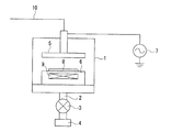
プラズマCVD法としては、周知のものが用いられ、例えば、図1に示すような平行平板型のプラズマ成膜装置などを使用して成膜することができる。
図1に示したプラズマ成膜装置は、減圧可能なチャンバー1を備え、このチャンバー1は、排気管2、開閉弁3を介して排気ポンプ4に接続されている。また、チャンバー1には、図示しない圧力計が備えられ、チャンバー1内の圧力が測定できるようになっている。チャンバー1内には、相対向する一対の平板状の上部電極5と下部電極6とが設けられている。上部電極5は、高周波電源7に接続され、上部電極5に高周波電流が印加されるようになっている。
As the plasma CVD method, a well-known method is used. For example, the film can be formed using a parallel plate type plasma film forming apparatus as shown in FIG.
The plasma film forming apparatus shown in FIG. 1 includes a chamber 1 that can be decompressed, and the chamber 1 is connected to an
下部電極6は、基板8を載置する載置台を兼ねており、その内部にはヒーター9が内蔵され、基板8を加熱できるようになっている。
また、上部電極5には、ガス供給配管10が接続されている。このガス供給配管10には、図示しない成膜用ガス供給源が接続され、この成膜用ガス供給装置からの成膜用のガスが供給され、このガスは上部電極5内に形成された複数の貫通孔を通って、下部電極6に向けて拡散しつつ流れ出るようになっている。
The
A
また、上記成膜用ガス供給源には、上述の絶縁膜材料を気化する気化装置と、その流量を調整する流量調整弁を備えるとともに、酸化剤およびキャリアガスを供給する供給装置がそれぞれ設けられており、これらのガスもガス供給配管10を流れて、上部電極5からチャンバー1内に流れ出るようになっている。
The film forming gas supply source includes a vaporizer for vaporizing the insulating film material and a flow rate adjusting valve for adjusting the flow rate, and a supply device for supplying an oxidant and a carrier gas. These gases also flow through the
プラズマ成膜装置のチャンバー1内の下部電極6上に基板8を置き、成膜用ガス供給源から上記成膜用ガスをチャンバー1内に送り込む。高周波電源7から高周波電流を上部電極5に印加して、チャンバー1内にプラズマを発生させる。これにより、基板8上に上記成膜用ガスから気相化学反応により生成した絶縁膜が形成される。
基板8には、主にシリコンウェーハからなるものが用いられるが、このシリコンウェーハ上にはあらかじめ形成された他の絶縁膜、導電膜、配線構造などが存在していてもよい。
The
The
プラズマCVD法としては、平行平板型の他に、ICPプラズマ、ECRプラズマ、マグネトロンプラズマ、高周波プラズマ、マイクロ波プラズマ、容量結合プラズマ、誘導結合プラズマなどを用いることが可能であり、平行平板型装置の下部電極にも高周波を導入する2周波励起プラズマを使用することもできる。 As the plasma CVD method, in addition to the parallel plate type, ICP plasma, ECR plasma, magnetron plasma, high frequency plasma, microwave plasma, capacitively coupled plasma, inductively coupled plasma, etc. can be used. It is also possible to use a two-frequency excitation plasma that introduces a high frequency to the lower electrode.
このプラズマ成膜装置における成膜条件は、以下の範囲が好適である。
絶縁膜材料流量 :25〜100cc/分 (2種以上の場合は合計量である)
キャリアガス流量 :0〜1000cc/分
酸化剤ガス流量 :1.25〜25cc/分
圧力 :1〜35Torr
RFパワー :100〜600W
基板温度 :200〜300℃
反応時間 :1秒〜1800秒
成膜厚さ :100nm〜300nm
The following ranges are suitable for the film forming conditions in this plasma film forming apparatus.
Insulating film material flow rate: 25 to 100 cc / min (in the case of 2 or more types, the total amount)
Carrier gas flow rate: 0 to 1000 cc / min Oxidant gas flow rate: 1.25 to 25 cc / min Pressure: 1 to 35 Torr
RF power: 100-600W
Substrate temperature: 200-300 ° C
Reaction time: 1 second to 1800 seconds Film thickness: 100 nm to 300 nm
上記成膜条件において、重要な点は、基板温度である。従来の成膜方法では、通常基板温度は350℃程度とされるが、本発明では基板の温度を200〜300℃の範囲とする。絶縁膜の比誘電率を低くするには、200℃程度がよく、機械的強度を高くするには300℃程度がよく、目的の物性に合わせて適宜選択することができる。
誘電率、強度、安定性の三者のバランスを重視した絶縁膜を形成する場合は250℃前後が好ましい。
In the film forming conditions, an important point is the substrate temperature. In the conventional film forming method, the substrate temperature is usually about 350 ° C., but in the present invention, the substrate temperature is set in the range of 200 to 300 ° C. In order to reduce the relative dielectric constant of the insulating film, about 200 ° C. is preferable, and in order to increase the mechanical strength, about 300 ° C. is preferable, and can be appropriately selected according to the desired physical properties.
In the case of forming an insulating film with an emphasis on the balance between the dielectric constant, strength, and stability, the temperature is preferably around 250 ° C.
また、酸化剤を同伴させずに成膜を行った場合、成膜後に不活性ガスと酸化剤との混合ガスをプラズマ成膜装置に流通させつつ、基板を加熱して絶縁膜の熱処理を行ってもよい。不活性ガスには例えば窒素が使用され、基板温度は例えば200〜300℃の範囲とされる。 In addition, when film formation is performed without accompanying an oxidant, the insulating film is heat-treated by heating the substrate while circulating a mixed gas of an inert gas and an oxidant through the plasma film formation apparatus after film formation. May be. For example, nitrogen is used as the inert gas, and the substrate temperature is in the range of 200 to 300 ° C., for example.
プラズマCVD法により成膜された絶縁膜は、ついで紫外線(UV)照射により後処理される。紫外線照射することで、絶縁膜中に存在する炭化水素を除去して、比誘電率を低くすることができる。例えば、除去される炭化水素としては、CxHy(x=1〜6、y=3〜11)がある。
紫外線照射法としては、周知のものが用いられ、例えば、図2に示すような紫外線照射装置などを使用する。
The insulating film formed by the plasma CVD method is then post-processed by ultraviolet (UV) irradiation. By irradiating with ultraviolet rays, hydrocarbons present in the insulating film can be removed and the relative dielectric constant can be lowered. For example, hydrocarbons to be removed include CxHy (x = 1 to 6, y = 3 to 11).
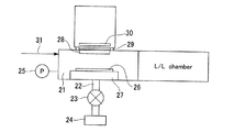
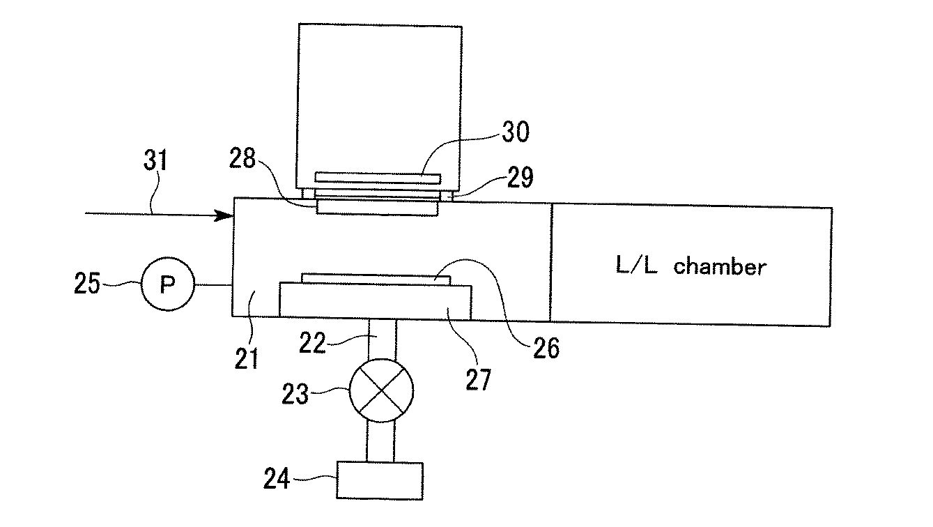
As the ultraviolet irradiation method, a well-known method is used, and for example, an ultraviolet irradiation device as shown in FIG. 2 is used.
図2に示した紫外線照射装置は、減圧可能なチャンバー21を備え、このチャンバー21は、排気管22、開閉弁23を介して排気ポンプ24に接続されている。また、チャンバー21には、圧力計25が備えられ、チャンバー21内の圧力が測定できるようになっている。さらに、チャンバー21内には、基板26を載置する載置台27に対向して、石英板28とシャッター29が設けられ、シャッター29の裏面には紫外線ランプ30が設けられている。
The ultraviolet irradiation apparatus shown in FIG. 2 includes a
基板26を載置する載置台27の内部には、図示しないヒーターが内蔵され、基板26を加熱できるようになっている。
また、チャンバー21にはガス供給配管31が接続されており、このガス供給配管31には、図示しない不活性ガス供給源が接続され、チャンバー21内を不活性雰囲気に保つことができる。不活性ガスには例えば窒素が使用される。
A heater (not shown) is built in the mounting table 27 for mounting the
Further, a
紫外線照射装置のチャンバー21内の載置台27上に基板26を載置して、載置台27に備えられたヒーターにより基板26を加熱しつつ、不活性ガス供給源から不活性ガスをチャンバー21内に流通させながら、紫外線照射を行う。これにより、基板26上にある絶縁膜が紫外線照射処理される。
The
この紫外線照射装置における紫外線照射条件は、以下の範囲が好適であるがこの限りではない。
不活性ガス流量 :0〜5slm
圧力 :10Torr以下
基板温度 :450℃以下、好ましくは350〜450℃
紫外線強度 :430mW/cm2程度
紫外線波長 :200nm以上、好ましくは350〜400nm
紫外線照射時間 :3〜6分
基板と紫外線ランプの距離:50〜150mm、好ましくは108mm
The following range is suitable for the ultraviolet irradiation conditions in this ultraviolet irradiation apparatus, but is not limited thereto.
Inert gas flow rate: 0-5 slm
Pressure: 10 Torr or less Substrate temperature: 450 ° C. or less, preferably 350 to 450 ° C.
UV intensity: about 430 mW / cm 2 UV wavelength: 200 nm or more, preferably 350 to 400 nm
UV irradiation time: 3 to 6 minutes Distance between substrate and UV lamp: 50 to 150 mm, preferably 108 mm
紫外線照射条件のなかで、紫外線の波長が重要な要素となる。この発明における紫外線照射処理は、絶縁膜の劣化を伴うことなく、実施する必要があり、短波長の高エネルギーの紫外線は用いることができず、比較的低エネルギーの200nm以上の波長の紫外線が用いられ、350〜400nmの波長が好ましい。200nm未満の波長の紫外線では、絶縁膜の劣化が生じる。 Among the UV irradiation conditions, the wavelength of the UV is an important factor. The ultraviolet irradiation treatment in this invention needs to be carried out without deteriorating the insulating film, and short wavelength high energy ultraviolet rays cannot be used, and relatively low energy ultraviolet rays having a wavelength of 200 nm or more are used. A wavelength of 350 to 400 nm is preferred. In the ultraviolet ray having a wavelength of less than 200 nm, the insulating film is deteriorated.
また、紫外線照射時間が短すぎると紫外線照射による効果が充分に絶縁膜内に行き渡らず、長すぎると絶縁膜の劣化が生じる。絶縁膜の膜厚が増すにつれて必要な照射時間も増加するが、最大でも6分を越えないことが好ましい。 If the ultraviolet irradiation time is too short, the effect of ultraviolet irradiation does not reach the insulating film sufficiently, and if it is too long, the insulating film deteriorates. Although the necessary irradiation time increases as the thickness of the insulating film increases, it is preferable not to exceed 6 minutes at the maximum.
他に、紫外線照射条件のなかでは、基板温度が熱的安定性に影響する。基板温度が低いと熱的安定性が低くなり、多層配線構造を形成する加熱工程で絶縁膜の劣化が生じる。
一方、基板温度が高いと熱的安定性が高くなるが、基板温度が高すぎると多層配線構造の熱的に弱い構造部分を劣化させてしまう恐れがあるため、350〜450℃の基板温度が好ましい。
In addition, among the ultraviolet irradiation conditions, the substrate temperature affects the thermal stability. When the substrate temperature is low, the thermal stability is lowered, and the insulating film is deteriorated in the heating process for forming the multilayer wiring structure.
On the other hand, if the substrate temperature is high, the thermal stability becomes high, but if the substrate temperature is too high, there is a risk of degrading the thermally weak structural portion of the multilayer wiring structure. preferable.
次に、本発明の絶縁膜について、説明する。
本発明の絶縁膜は、上述のプラズマCVD用絶縁膜材料と酸化剤またはこれとキャリアガスとを用い、プラズマ成膜装置によってプラズマCVD反応により成膜された後、紫外線照射処理されたもので、その比誘電率が低くで、機械的強度が高く、空気雰囲気中での安定性および熱的安定性が高いものである。
Next, the insulating film of the present invention will be described.
The insulating film of the present invention is a film formed by a plasma CVD reaction by a plasma film forming apparatus using the above-described plasma CVD insulating film material and an oxidizing agent or a carrier gas, and then subjected to ultraviolet irradiation treatment. The relative dielectric constant is low, the mechanical strength is high, and the stability in the air atmosphere and the thermal stability are high.
すなわち、得られた絶縁膜の比誘電率は少なくとも2.4以下で2.3程度のものとなり、大気圧下で空気雰囲気中に14日間放置した後の比誘電率の変化率(Δk)が2%以下、好ましくは1%以下であるものである。
この絶縁膜は、ケイ素と水素と炭素と酸素から構成されている。
That is, the relative dielectric constant of the obtained insulating film is at least 2.4 or less and about 2.3, and the change rate (Δk) of the relative dielectric constant after being left in an air atmosphere at atmospheric pressure for 14 days is 2% or less, preferably 1% or less.
This insulating film is composed of silicon, hydrogen, carbon, and oxygen.
本発明の絶縁膜形成方法により得られた絶縁膜が、優れた機械的強度を有し、かつ空気雰囲気中での安定性および熱的安定性が高く、低比誘電率を有する理由は、以下のように推測される。
プラズマ成膜装置によってプラズマCVD反応により形成された絶縁膜は、CxHy、水素終端されたSi−H、架橋されたSi−Oで構成されている。Si−Hは比誘電率に対する寄与が大きく、Si−Oは絶縁膜を形成するための主骨格の役割がある。
The insulating film obtained by the insulating film forming method of the present invention has excellent mechanical strength, high stability in the air atmosphere and high thermal stability, and the reason for having a low dielectric constant is as follows. Is guessed.
The insulating film formed by the plasma CVD reaction by the plasma film forming apparatus is composed of CxHy, hydrogen-terminated Si—H, and cross-linked Si—O. Si-H greatly contributes to the relative dielectric constant, and Si-O plays a role of a main skeleton for forming an insulating film.
絶縁膜を構成するCxHyの量は、プラズマ成膜装置に設けられた基板8の温度に依存する。できる限りCxHyを適量導入するには、該基板温度は200〜300℃の範囲とされる。
比誘電率を低くするためには、絶縁膜構造中の空孔を増加させること、絶縁膜を構成するSi−Hを減少させることに関与する。
The amount of CxHy constituting the insulating film depends on the temperature of the
In order to reduce the relative dielectric constant, it is involved in increasing the number of vacancies in the insulating film structure and decreasing Si—H constituting the insulating film.
絶縁膜構造中の空孔を増加させるには、紫外線照射により絶縁膜を構成するCxHyを除去する。つまり、プラズマ成膜装置によって成膜された絶縁膜中にCxHyの量が多ければ、紫外線照射により絶縁膜構造中の空孔を増加させることができる。CxHyの量はプラズマ成膜装置の成膜温度すなわち基板温度に依存し、基板温度が低いと成膜後の絶縁膜中のCxHy量は多くなる。 In order to increase the number of holes in the insulating film structure, CxHy constituting the insulating film is removed by ultraviolet irradiation. That is, if the amount of CxHy is large in the insulating film formed by the plasma film forming apparatus, the number of holes in the insulating film structure can be increased by ultraviolet irradiation. The amount of CxHy depends on the deposition temperature of the plasma deposition apparatus, that is, the substrate temperature. When the substrate temperature is low, the amount of CxHy in the insulating film after deposition increases.
絶縁膜を構成するCxHyの除去量は、紫外線強度、紫外線波長および基板温度に依存する。紫外線強度は紫外線照射装置に設けられた前記基板温度に影響を与えるため、使用する紫外線照射装置によって管理する。紫外線波長は、短波長(高エネルギー)の紫外線光より長波長(低エネルギー)の紫外線光のほうが好ましい。紫外線照射時間が長い場合は、絶縁膜が収縮するとともに絶縁膜中の空孔が収縮するため、比誘電率が高くなる。 The amount of CxHy that forms the insulating film depends on the ultraviolet intensity, the ultraviolet wavelength, and the substrate temperature. Since the ultraviolet intensity affects the temperature of the substrate provided in the ultraviolet irradiation apparatus, it is controlled by the ultraviolet irradiation apparatus used. The ultraviolet wavelength is preferably long wavelength (low energy) ultraviolet light rather than short wavelength (high energy) ultraviolet light. When the ultraviolet irradiation time is long, the insulating film contracts and the vacancies in the insulating film contract, so that the relative dielectric constant increases.
なお、紫外線照射装置に設けられたチャンバー21内に水分等が存在すると、該絶縁膜を構成する炭化水素が絶縁膜から除去されるとともに、該水分等が該絶縁膜に吸着して、比誘電率を上昇させるため、不活性ガスをチャンバーに流通させる。
If moisture or the like is present in the
絶縁膜を構成するSi−Hを減少させるには、絶縁膜材料に酸化剤ガスを同伴させてプラズマCVD法により成膜する。前記絶縁膜を構成するSi−Hと反応して、Si−Oを形成するとともにSi−Hが減少する。同伴させる酸化剤ガスの量が多すぎると、Si−Oが過剰に形成されるとともに絶縁膜の密度が高くなるため、比誘電率が低下しない。 In order to reduce Si—H constituting the insulating film, the insulating film material is formed by a plasma CVD method with an oxidant gas. It reacts with Si—H constituting the insulating film to form Si—O and Si—H decreases. When the amount of the oxidant gas to be accompanied is too large, Si—O is excessively formed and the density of the insulating film increases, so that the relative dielectric constant does not decrease.
機械的強度を高くするには、絶縁膜を構成するSi−O量を増加させればよい。Si−Oはプラズマ成膜装置の成膜温度すなわち基板温度に依存し、基板温度が高いと形成される絶縁膜中のSi−O量は多くなる。また、絶縁膜材料に酸化剤ガスを同伴させ、Si−HをSi−Oに変化させることでSi−O量を増加させることができる。しかし、Si−Oが過剰に形成されると絶縁膜の密度が高くなり、機械的強度は高くなるが、比誘電率が低下しない。 In order to increase the mechanical strength, the amount of Si—O constituting the insulating film may be increased. Si—O depends on the film forming temperature of the plasma film forming apparatus, that is, the substrate temperature. When the substrate temperature is high, the amount of Si—O in the formed insulating film increases. In addition, the amount of Si—O can be increased by entraining the insulating film material with an oxidant gas and changing Si—H to Si—O. However, when Si—O is excessively formed, the density of the insulating film increases and the mechanical strength increases, but the relative dielectric constant does not decrease.
絶縁膜の空孔率を増加させると、絶縁膜の空気に触れる部分が増加するとともに、絶縁膜構造内で主に絶縁膜中のSi−Hが徐々に空気雰囲気中の酸素または水分と反応して誘電率が経時的に高くなる。 Increasing the porosity of the insulating film increases the portion of the insulating film that comes into contact with air, and Si-H in the insulating film gradually reacts with oxygen or moisture in the air atmosphere in the insulating film structure. The dielectric constant increases with time.
空気雰囲気中での保存安定性を高くするには、絶縁膜中のSi−Hを減少させることで可能であり、Si−Hを減少させるには、酸化剤を同伴した条件で成膜を行うことで達成できる。絶縁膜中にSi−Hが存在すると、これが空気雰囲気中の酸素または水分と反応してSi−OHに変化して、比誘電率が高くなって、保存安定性が悪くなる。 In order to increase the storage stability in the air atmosphere, it is possible to reduce Si—H in the insulating film, and in order to reduce Si—H, film formation is performed under conditions accompanied by an oxidizing agent. Can be achieved. If Si—H is present in the insulating film, it reacts with oxygen or moisture in the air atmosphere and changes to Si—OH, resulting in an increase in relative dielectric constant and poor storage stability.
また、紫外線照射により絶縁膜の熱的安定性が向上する。すなわち、プラズマCVD法によって成膜されたままの絶縁膜中には、不安定なCxHyが多量に存在すると考えられ、紫外線照射によって、不安定なCxHy結合を除去できる。このように、熱的安定性を損ねる恐れのある不安定なCxHyが取り除かれることで、熱的安定性が向上するものと推定される。
以上より、本発明にかかる絶縁膜が、低比誘電率を有し、かつ高い機械的強度、高い空気雰囲気中の安定性、高い熱的安定性を有する絶縁膜となるものと考えられる。
In addition, the thermal stability of the insulating film is improved by ultraviolet irradiation. That is, it is considered that a large amount of unstable CxHy is present in the insulating film that has been formed by the plasma CVD method, and unstable CxHy bonds can be removed by ultraviolet irradiation. Thus, it is presumed that the thermal stability is improved by removing unstable CxHy that may impair the thermal stability.
From the above, it is considered that the insulating film according to the present invention is an insulating film having a low relative dielectric constant, high mechanical strength, high stability in an air atmosphere, and high thermal stability.
以下、本発明を実施例および比較例によりさらに詳細に説明する。
ただし、本発明は以下の実施例によって何ら限定されるものではない。
Hereinafter, the present invention will be described in more detail with reference to Examples and Comparative Examples.
However, the present invention is not limited to the following examples.
(実施例1)
絶縁膜を形成するにあたっては、平行平板型の容量結合プラズマCVD装置を使用し、
あらかじめ250℃程度に加熱したサセプター上に、8インチ(直径200mm)または
12インチ(直径300mm)のシリコンウェーハを搬送し、絶縁膜材料ガスとしてジシクロペンチルジメトキシシランを30cc/minの体積流量で、キャリアガスとしてヘリウムを600cc/min、酸素ガスを4cc/minを同伴して流通させ、プラズマ発生用高周波電源装置の出力を300Wに設定して絶縁膜を形成した。このときの前記プラズマCVD装置のチャンバー内圧力は35Torrであった。
Example 1
In forming the insulating film, using a parallel plate type capacitively coupled plasma CVD apparatus,
An 8-inch (diameter 200 mm) or 12-inch (diameter 300 mm) silicon wafer is transferred onto a susceptor that has been heated to about 250 ° C. in advance, and dicyclopentyldimethoxysilane is used as an insulating film material gas at a volume flow rate of 30 cc / min. Helium was circulated as a gas at 600 cc / min and oxygen gas was circulated at 4 cc / min, and the output of the high frequency power supply for plasma generation was set to 300 W to form an insulating film. At this time, the pressure in the chamber of the plasma CVD apparatus was 35 Torr.
プラズマ成膜装置によってプラズマCVD反応により成膜された絶縁膜を改質するにあたっては、紫外線照射装置を使用し、あらかじめ400℃程度に加熱した載置台上に、8インチ(直径200mm)または12インチ(直径300mm)のシリコンウェーハを搬送し、窒素ガスを2000cc/minの体積流量で流通させ、紫外線波長350nm程度、紫外線強度430mW/cm2程度、ウェーハと紫外線ランプの距離を108mm、紫外線照射時間を5分程度に設定して、絶縁膜を改質した。このときの前記紫外線照射装置のチャンバー内圧力は5Torrであった。 In modifying an insulating film formed by a plasma CVD reaction by a plasma film forming apparatus, an ultraviolet irradiation apparatus is used and is placed on a mounting table preliminarily heated to about 400 ° C., 8 inches (diameter 200 mm) or 12 inches. A silicon wafer (diameter 300 mm) is conveyed, nitrogen gas is circulated at a volume flow rate of 2000 cc / min, an ultraviolet wavelength of about 350 nm, an ultraviolet intensity of about 430 mW / cm 2 , a distance between the wafer and the ultraviolet lamp of 108 mm, and an ultraviolet irradiation time. The insulating film was modified for about 5 minutes. At this time, the pressure in the chamber of the ultraviolet irradiation device was 5 Torr.
得られた絶縁膜の比誘電率を測定するために、前記シリコンウェーハをSSM社製CV測定装置495上に搬送し、水銀電極を用いて絶縁膜の比誘電率を測定した。測定結果を表1に示す。 In order to measure the relative dielectric constant of the obtained insulating film, the silicon wafer was transferred onto a CV measuring device 495 manufactured by SSM, and the relative dielectric constant of the insulating film was measured using a mercury electrode. The measurement results are shown in Table 1.
得られた絶縁膜の機械的強度を測定するために、MTS社製Nano Indenter DCMを使用した。該絶縁膜のヤング率を機械的強度とした。該測定装置に設けられた圧子の押し込み深さは、該絶縁膜の厚さの10%程度とした。測定結果を表1に示す。 In order to measure the mechanical strength of the obtained insulating film, Nano Indenter DCM manufactured by MTS was used. The Young's modulus of the insulating film was defined as mechanical strength. The indentation depth of the indenter provided in the measuring apparatus was about 10% of the thickness of the insulating film. The measurement results are shown in Table 1.
得られた絶縁膜の熱的安定性を評価する方法として、該絶縁膜を400℃で10分間加熱した後、比誘電率を測定した。加熱と測定を3回繰り返すことで、該絶縁膜が多層配線構造を形成する過程で加熱される様態を再現している。評価結果を表1に示す。 As a method for evaluating the thermal stability of the obtained insulating film, the insulating film was heated at 400 ° C. for 10 minutes, and then the relative dielectric constant was measured. By repeating the heating and measurement three times, the state in which the insulating film is heated in the process of forming the multilayer wiring structure is reproduced. The evaluation results are shown in Table 1.
得られた絶縁膜の空気雰囲気中での安定性を評価する方法として、該絶縁膜を空気雰囲気中に放置して、比誘電率の経時変化を測定した。この評価方法は、多層配線構造を形成する過程における、該絶縁膜の空気雰囲気中での放置を再現している。例えば、放置期間は2週間程度である。評価結果を表1に示す。 As a method for evaluating the stability of the obtained insulating film in an air atmosphere, the insulating film was left in an air atmosphere, and a change with time in relative permittivity was measured. This evaluation method reproduces the leaving of the insulating film in the air atmosphere in the process of forming the multilayer wiring structure. For example, the neglect period is about two weeks. The evaluation results are shown in Table 1.
(実施例2)
絶縁膜を形成するにあたって使用する装置および方法は実施例1とほぼ同じであるが、
絶縁膜材料ガスとしてジシクロヘキシルジメトキシシランを30cc/minの体積流量で、キャリアガスとしてヘリウムを600cc/min、酸素ガスを4cc/min同伴して流通させ、プラズマ発生用高周波電源装置の出力を300Wに設定して絶縁膜を形成した。このときの前記プラズマCVD装置のチャンバー内圧力は35Torrであった。
(Example 2)
The apparatus and method used to form the insulating film are almost the same as those in Example 1,
Dicyclohexyldimethoxysilane as an insulating film material gas is circulated at a volume flow rate of 30 cc / min, helium as carrier gas at 600 cc / min and oxygen gas at 4 cc / min, and the output of the high frequency power supply for plasma generation is set to 300 W. Thus, an insulating film was formed. At this time, the pressure in the chamber of the plasma CVD apparatus was 35 Torr.
また、成膜後の絶縁膜を紫外線照射処理するにあたって使用した装置および方法は実施例1と同じである。 The apparatus and method used for the ultraviolet irradiation treatment of the insulating film after film formation are the same as those in the first embodiment.
得られた絶縁膜の比誘電率、機械的強度、熱的安定性、空気雰囲気での安定性を実施例1と同様にして評価した。比誘電率、機械的強度、熱的安定性、空気雰囲気での安定性の測定結果を表1に示す。 The dielectric constant, mechanical strength, thermal stability, and stability in the air atmosphere of the obtained insulating film were evaluated in the same manner as in Example 1. Table 1 shows the measurement results of relative permittivity, mechanical strength, thermal stability, and stability in an air atmosphere.
(比較例1)
絶縁膜を形成するにあたって使用する装置および方法は実施例1とほぼ同じであるが、
サセプターをあらかじめ275℃程度に加熱して、絶縁膜材料ガスとしてジシクロペンチルジメトキシシランを30cc/minの体積流量で、キャリアガスとしてヘリウムを600cc/minを同伴して流通させ、プラズマ発生用高周波電源装置の出力を300Wに設定して絶縁膜を形成した。このときの前記プラズマCVD装置のチャンバー内圧力は35Torrであった。
この例では、酸化剤を同伴していない。
(Comparative Example 1)
The apparatus and method used to form the insulating film are almost the same as those in Example 1,
A susceptor is preheated to about 275 ° C., dicyclopentyldimethoxysilane as an insulating film material gas is circulated at a volume flow rate of 30 cc / min, and helium as a carrier gas is circulated along with 600 cc / min to generate a high frequency power supply for plasma generation Was set to 300 W to form an insulating film. At this time, the pressure in the chamber of the plasma CVD apparatus was 35 Torr.
In this example, no oxidant is involved.
また、成膜後の絶縁膜を紫外線照射処理するにあたって使用した装置および方法は実施例1と同じである。 The apparatus and method used for the ultraviolet irradiation treatment of the insulating film after film formation are the same as those in the first embodiment.
得られた絶縁膜の比誘電率、機械的強度、熱的安定性、空気雰囲気での安定性を実施例1と同様にして評価した。比誘電率、機械的強度、熱的安定性、空気雰囲気での安定性の測定結果を表1に示す。 The dielectric constant, mechanical strength, thermal stability, and stability in the air atmosphere of the obtained insulating film were evaluated in the same manner as in Example 1. Table 1 shows the measurement results of relative permittivity, mechanical strength, thermal stability, and stability in an air atmosphere.
(比較例2)
絶縁膜を形成するにあたって使用する装置および方法は実施例1とほぼ同じであるが、
サセプターをあらかじめ275℃程度に加熱して、絶縁膜材料ガスとしてジシクロペンチルジメトキシシランを30cc/minの体積流量で、キャリアガスとしてヘリウムを600cc/min、酸素ガスを4cc/min同伴して流通させ、プラズマ発生用高周波電源装置の出力を300Wに設定して絶縁膜を形成した。このときの前記プラズマCVD装置のチャンバー内圧力は35Torrであった。
(Comparative Example 2)
The apparatus and method used to form the insulating film are almost the same as those in Example 1,
The susceptor is preheated to about 275 ° C., dicyclopentyldimethoxysilane as an insulating film material gas is supplied at a volume flow rate of 30 cc / min, helium as a carrier gas is 600 cc / min, and oxygen gas is accompanied by 4 cc / min. The output of the plasma generating high frequency power supply device was set to 300 W to form an insulating film. At this time, the pressure in the chamber of the plasma CVD apparatus was 35 Torr.
成膜された絶縁膜には、紫外線照射処理を施していない。 The formed insulating film is not subjected to ultraviolet irradiation treatment.
得られた絶縁膜の比誘電率、機械的強度を実施例1と同様にして評価した。比誘電率、機械的強度の測定結果を表1に示す。 The dielectric constant and mechanical strength of the obtained insulating film were evaluated in the same manner as in Example 1. Table 1 shows the measurement results of relative dielectric constant and mechanical strength.
(比較例3)
絶縁膜を形成するにあたって使用する装置および方法は実施例1とほぼ同じであるが、
サセプターをあらかじめ275℃程度に加熱して、絶縁膜材料ガスとしてジシクロペンチルジメトキシシランを30cc/minの体積流量で、キャリアガスとしてヘリウムを600cc/min、酸素ガスを4cc/min同伴して流通させ、プラズマ発生用高周波電源装置の出力を300Wに設定して絶縁膜を形成した。このときの前記プラズマCVD装置のチャンバー内圧力は35Torrであった。
(Comparative Example 3)
The apparatus and method used to form the insulating film are almost the same as those in Example 1,
The susceptor is preheated to about 275 ° C., dicyclopentyldimethoxysilane as an insulating film material gas is supplied at a volume flow rate of 30 cc / min, helium as a carrier gas is 600 cc / min, and oxygen gas is accompanied by 4 cc / min. The output of the plasma generating high frequency power supply device was set to 300 W to form an insulating film. At this time, the pressure in the chamber of the plasma CVD apparatus was 35 Torr.
また、成膜後の絶縁膜を紫外線照射処理するにあったって使用する装置および方法は実施例1とほぼ同じであるが、紫外線波長172nm程度、紫外線強度20mW/cm2程度に設定して絶縁膜を改質させた。 The apparatus and method used for the ultraviolet irradiation treatment of the insulating film after film formation are substantially the same as in Example 1, but the insulating film is set to an ultraviolet wavelength of about 172 nm and an ultraviolet intensity of about 20 mW / cm 2. Was modified.
得られた絶縁膜の比誘電率、機械的強度、空気雰囲気での安定性を実施例1と同様にして評価した。比誘電率、機械的強度、空気雰囲気での安定性の測定結果を表1に示す。 The dielectric constant, mechanical strength, and stability in the air atmosphere of the obtained insulating film were evaluated in the same manner as in Example 1. Table 1 shows the measurement results of relative permittivity, mechanical strength, and stability in an air atmosphere.
(比較例4)
絶縁膜を形成するにあたって使用する装置および方法は実施例1とほぼ同じであるが、
サセプターをあらかじめ275℃程度に加熱して、絶縁膜材料ガスとしてジシクロペンチルジメトキシシランを30cc/minの体積流量で、キャリアガスとしてヘリウムを600cc/min、酸素ガスを4cc/min同伴して流通させ、プラズマ発生用高周波電源装置の出力を300Wに設定して絶縁膜を形成した。このときの前記プラズマCVD装置のチャンバー内圧力は35Torrであった。
(Comparative Example 4)
The apparatus and method used to form the insulating film are almost the same as those in Example 1,
The susceptor is preheated to about 275 ° C., dicyclopentyldimethoxysilane as an insulating film material gas is supplied at a volume flow rate of 30 cc / min, helium as a carrier gas is 600 cc / min, and oxygen gas is accompanied by 4 cc / min. The output of the plasma generating high frequency power supply device was set to 300 W to form an insulating film. At this time, the pressure in the chamber of the plasma CVD apparatus was 35 Torr.
成膜後の絶縁膜を紫外線照射処理するにあたって使用する装置および方法は実施例1と同じである。 The apparatus and method used for the ultraviolet irradiation treatment of the insulating film after film formation are the same as those in the first embodiment.
得られた絶縁膜の比誘電率、機械的強度、空気雰囲気での安定性を実施例1と同様にして評価した。比誘電率、機械的強度、空気雰囲気での安定性の測定結果を表1に示す。 The dielectric constant, mechanical strength, and stability in the air atmosphere of the obtained insulating film were evaluated in the same manner as in Example 1. Table 1 shows the measurement results of relative permittivity, mechanical strength, and stability in an air atmosphere.
表1に示した結果から、実施例1で得られた絶縁膜は比誘電率が2.37、ヤング率が8.0GPa、2週間程度空気雰囲気中に放置した場合の比誘電率の上昇率が1%未満、比誘電率の加熱による変化なしであった。
実施例2で得られた絶縁膜は比誘電率が2.30、ヤング率が7.0GPa、2週間程度空気雰囲気中に放置した場合の比誘電率の上昇率が1%未満、比誘電率の加熱による変化なしであることがわかった。
From the results shown in Table 1, the insulating film obtained in Example 1 has a relative dielectric constant of 2.37, a Young's modulus of 8.0 GPa, and an increase rate of the relative dielectric constant when left in an air atmosphere for about two weeks. Was less than 1% and the dielectric constant was not changed by heating.
The insulating film obtained in Example 2 has a relative dielectric constant of 2.30, a Young's modulus of 7.0 GPa, a relative dielectric constant increase rate of less than 1% when left in an air atmosphere for about 2 weeks, and a relative dielectric constant. It was found that there was no change due to heating.
表1に示した結果から、比較例1で得られた絶縁膜は比誘電率が2.47、ヤング率が8.9GPa、2週間程度空気雰囲気中に放置した場合の比誘電率の上昇率が3%程度であることがわかった。 From the results shown in Table 1, the insulating film obtained in Comparative Example 1 has a relative dielectric constant of 2.47, a Young's modulus of 8.9 GPa, and an increase rate of the relative dielectric constant when left in an air atmosphere for about 2 weeks. Was found to be about 3%.
比較例1より、空気雰囲気中に放置すると比誘電率が大きくなることがわかった。したがって、多層配線構造を形成する過程において、絶縁膜を空気雰囲気中で放置すれば、配線層間容量を減らすことができないことがわかった。 From Comparative Example 1, it was found that the dielectric constant increased when left in an air atmosphere. Accordingly, it has been found that if the insulating film is left in the air atmosphere in the process of forming the multilayer wiring structure, the wiring interlayer capacitance cannot be reduced.
表1に示した結果から、比較例2で形成され改質された絶縁膜は比誘電率が2.70、ヤング率が5.0GPaであることがわかった。比較例2より、紫外線照射による絶縁膜の改質を行わなければ、比誘電率が小さくならないことがわかった。また、熱的安定性も確保できないことがわかった。 From the results shown in Table 1, it was found that the insulating film formed and modified in Comparative Example 2 had a relative dielectric constant of 2.70 and a Young's modulus of 5.0 GPa. From Comparative Example 2, it was found that the dielectric constant would not be reduced unless the insulating film was modified by ultraviolet irradiation. It was also found that thermal stability could not be ensured.
表1に示した結果および図3で示したグラフから、比較例3で形成され改質された絶縁膜は比誘電率が2.60、ヤング率が9.2GPa、2週間程度空気雰囲気中に放置した場合の比誘電率の上昇率が10%程度、比誘電率の加熱による変化なしであることがわかった。 From the results shown in Table 1 and the graph shown in FIG. 3, the modified insulating film formed in Comparative Example 3 has a relative dielectric constant of 2.60, a Young's modulus of 9.2 GPa, and in an air atmosphere for about two weeks. It was found that the increase rate of the relative permittivity when it was allowed to stand was about 10%, and the relative permittivity did not change due to heating.
比較例3より、短波長紫外線の照射による絶縁膜の改質を行っても、該絶縁膜の空気雰囲気中での安定性が低いことがわかった。 From Comparative Example 3, it was found that even when the insulating film was modified by irradiation with short wavelength ultraviolet rays, the stability of the insulating film in the air atmosphere was low.
表1に示した結果から、比較例4で形成され改質された絶縁膜は比誘電率が2.50、ヤング率が9.2GPa、2週間程度空気雰囲気中に放置した場合の比誘電率の上昇率が1%未満であることがわかった。 From the results shown in Table 1, the insulating film formed and modified in Comparative Example 4 has a relative dielectric constant of 2.50, a Young's modulus of 9.2 GPa, and a relative dielectric constant when left in an air atmosphere for about two weeks. It was found that the rate of increase was less than 1%.
比較例4より、プラズマ成膜装置で絶縁膜を形成する際の成膜温度が高かったために、得られた絶縁膜の比誘電率が比較的大きくなることがわかった。 From Comparative Example 4, it was found that the dielectric constant of the obtained insulating film was relatively large because the film forming temperature when forming the insulating film with the plasma film forming apparatus was high.
このように、前記化学式(1)で示されるケイ素化合物からなる絶縁膜材料を用いてプ
ラズマCVD法によって絶縁膜を適切な成膜温度で成膜して、適切な紫外線照射により該絶縁膜を改質することで、機械的強度、空気雰囲気中の安定性、熱的安定性が高くかつ比誘電率が低い絶縁膜を形成するができる。
Thus, an insulating film is formed at an appropriate film formation temperature by a plasma CVD method using an insulating film material made of a silicon compound represented by the chemical formula (1), and the insulating film is modified by appropriate ultraviolet irradiation. Therefore, it is possible to form an insulating film having high mechanical strength, stability in an air atmosphere, high thermal stability and low relative dielectric constant.
本発明は、次世代に求められる高集積化されたLSI配線を使用する半導体装置に適用することができる。 The present invention can be applied to a semiconductor device using highly integrated LSI wiring required for the next generation.
1・・チャンバー、2・・排気管、3・・開閉弁、4・・排気ポンプ、5・・上部電極、6・・下部電極、7・・高周波電源、8・・基板、9・・ヒータ、10・・ガス供給配管、21・・チャンバー、22・・排気管、23・・開閉弁、24・・排気ポンプ、25・・圧力計、26・・基板(ウェーハ)、27・・載置台(サセプタ)、28・・石英板、29・・シャッター、30・・紫外線ランプ、31・・ガス供給配管
1 .... Chamber, 2 .... Exhaust pipe, 3 .... Open / close valve, 4 .... Exhaust pump, 5 .... Upper electrode, 6 .... Lower electrode, 7 .... High frequency power supply, 8 .... Substrate, 9 ...
Claims (7)
成膜の際、酸化剤を同伴させるとともに、成膜温度を200℃〜300℃とし、ついで絶縁膜に200nm以上の波長の紫外線を照射する絶縁膜の成膜方法。
R1およびR2は、CH3、C2H5、n−C3H7、iso−C3H7、n−C4H9、iso−C4H9、tert−C4H9のいずれかであり、R1およびR2とは、一分子中において同一でも互いに相違であっても良い。
R3およびR4は、
c−C4X7、c−C5X9、c−C6X11、
c−C4X5、c−C5X7、c−C6X9、
c−C5X5、c−C6X7、
c−C6X5
のいずれかであり、R3およびR4とは、一分子中において同一でも互いに相違であっても良い。
前記R3、R4において、
Xは、H、CH3、C2H5、n−C3H7、iso−C3H7、n−C4H9、iso−C4H9、tert−C4H9のいずれかである。 A film forming method for forming an insulating film by a plasma CVD method using an insulating film material for plasma CVD represented by the following chemical formula (1):
A method for forming an insulating film in which an oxidant is accompanied during film formation, the film forming temperature is set to 200 ° C. to 300 ° C., and then the ultraviolet light having a wavelength of 200 nm or more is irradiated to the insulating film.
R 1 and R 2 are CH 3 , C 2 H 5 , n-C 3 H 7 , iso-C 3 H 7 , n-C 4 H 9 , iso-C 4 H 9 , tert-C 4 H 9 . R 1 and R 2 may be the same or different from each other in one molecule.
R 3 and R 4 are
c-C 4 X 7, c -C 5 X 9, c-C 6 X 11,
c-C 4 X 5 , c-C 5 X 7 , c-C 6 X 9 ,
c-C 5 X 5 , c-C 6 X 7 ,
c-C 6 X 5
R 3 and R 4 may be the same or different from each other in one molecule.
In R 3 and R 4 ,
X is any one of H, CH 3 , C 2 H 5 , n-C 3 H 7 , iso-C 3 H 7 , n-C 4 H 9 , iso-C 4 H 9 , and tert-C 4 H 9 . It is.
Priority Applications (1)
| Application Number | Priority Date | Filing Date | Title |
|---|---|---|---|
| JP2008124604A JP2009277686A (en) | 2008-05-12 | 2008-05-12 | Method of forming insulating film, and insulating film |
Applications Claiming Priority (1)
| Application Number | Priority Date | Filing Date | Title |
|---|---|---|---|
| JP2008124604A JP2009277686A (en) | 2008-05-12 | 2008-05-12 | Method of forming insulating film, and insulating film |
Publications (1)
| Publication Number | Publication Date |
|---|---|
| JP2009277686A true JP2009277686A (en) | 2009-11-26 |
Family
ID=41442885
Family Applications (1)
| Application Number | Title | Priority Date | Filing Date |
|---|---|---|---|
| JP2008124604A Pending JP2009277686A (en) | 2008-05-12 | 2008-05-12 | Method of forming insulating film, and insulating film |
Country Status (1)
| Country | Link |
|---|---|
| JP (1) | JP2009277686A (en) |
Citations (7)
| Publication number | Priority date | Publication date | Assignee | Title |
|---|---|---|---|---|
| JPH0848543A (en) * | 1994-04-19 | 1996-02-20 | Boc Group Inc:The | Plasma-strengthened chemical vapor deposition of anticlouding and scratch-resistant coating on varions substrates |
| JPH08321499A (en) * | 1995-03-20 | 1996-12-03 | Fujitsu Ltd | Silicon compound film and forming method thereof |
| JP2002526219A (en) * | 1998-09-21 | 2002-08-20 | ザ、プロクター、エンド、ギャンブル、カンパニー | Liquid permeable web that is durably wettable |
| JP2004274052A (en) * | 2003-03-04 | 2004-09-30 | Air Products & Chemicals Inc | Mechanical enhancement of high-density porous organic silicate material by uv irradiation |
| JP2005051192A (en) * | 2002-11-28 | 2005-02-24 | Tosoh Corp | Material for insulating film containing organic silane and organic siloxane compounds, manufacturing method thereof, and semiconductor device |
| WO2006075578A1 (en) * | 2005-01-12 | 2006-07-20 | Tri Chemical Laboratories Inc. | Film forming material and method of film forming |
| JP2007523484A (en) * | 2004-02-19 | 2007-08-16 | デグサ ゲーエムベーハー | Silicone compound for forming SiO2-containing insulating layer on chips |
-
2008
- 2008-05-12 JP JP2008124604A patent/JP2009277686A/en active Pending
Patent Citations (7)
| Publication number | Priority date | Publication date | Assignee | Title |
|---|---|---|---|---|
| JPH0848543A (en) * | 1994-04-19 | 1996-02-20 | Boc Group Inc:The | Plasma-strengthened chemical vapor deposition of anticlouding and scratch-resistant coating on varions substrates |
| JPH08321499A (en) * | 1995-03-20 | 1996-12-03 | Fujitsu Ltd | Silicon compound film and forming method thereof |
| JP2002526219A (en) * | 1998-09-21 | 2002-08-20 | ザ、プロクター、エンド、ギャンブル、カンパニー | Liquid permeable web that is durably wettable |
| JP2005051192A (en) * | 2002-11-28 | 2005-02-24 | Tosoh Corp | Material for insulating film containing organic silane and organic siloxane compounds, manufacturing method thereof, and semiconductor device |
| JP2004274052A (en) * | 2003-03-04 | 2004-09-30 | Air Products & Chemicals Inc | Mechanical enhancement of high-density porous organic silicate material by uv irradiation |
| JP2007523484A (en) * | 2004-02-19 | 2007-08-16 | デグサ ゲーエムベーハー | Silicone compound for forming SiO2-containing insulating layer on chips |
| WO2006075578A1 (en) * | 2005-01-12 | 2006-07-20 | Tri Chemical Laboratories Inc. | Film forming material and method of film forming |
Similar Documents
| Publication | Publication Date | Title |
|---|---|---|
| TWI706053B (en) | Precursors and flowable cvd methods for making low-k films to fill surface features | |
| JP5268130B2 (en) | Method for forming an oxygen-containing silicon carbide film | |
| JP2020065087A (en) | Formation of SiOCN thin film | |
| JP6845252B2 (en) | Compositions for depositing silicon-containing membranes and methods using them | |
| JP6959334B2 (en) | Use of Cyril Crosslinked Alkyl Compounds for High Density OSG Membranes | |
| JP4344841B2 (en) | Method for forming low dielectric constant insulating film | |
| JP5312588B2 (en) | Novel silicon precursor for making ultra-low K films with high mechanical properties by plasma enhanced chemical vapor deposition | |
| CN101316945B (en) | A method to improve the ashing/wet etch damage resistance and integration stability of low dielectric constant films | |
| JP2005117052A (en) | Method of manufacturing silicon carbide film | |
| JP5614589B2 (en) | Film forming method using insulating film material and insulating film | |
| JP2004320005A (en) | Chemical vapor deposition process for fabricating porous organic silica film | |
| JP2013211592A (en) | Method for removal of carbon from organic silicate material | |
| TWI388687B (en) | Novel silicon precursors to make ultra low-k films with high mechanical properties by plasma enhanced chemical vapor deposition | |
| TWI729417B (en) | Silicon compounds and methods for depositing films using same | |
| KR20180092309A (en) | Low k precursors providing superior integration attributes | |
| TW202117058A (en) | Silicon compounds and methods for depositing films using same | |
| JP2009289996A (en) | Method for manufacturing semiconductor device, and semiconductor device | |
| KR100926722B1 (en) | The siloxane polymer film on a semiconductor substrate and its manufacturing method | |
| JP2009277686A (en) | Method of forming insulating film, and insulating film | |
| JP3197008B2 (en) | Silicon polymer insulating film on semiconductor substrate and method for forming the film | |
| TWI762761B (en) | Use of silicon structure former with organic substituted hardening additive compounds for dense osg films | |
| JP2008263022A (en) | Insulating film material, film forming method employing the insulating film material, and insulating film | |
| TWI822044B (en) | Composition for vapor deposition of dielectric film and method for depositing organosilica film | |
| JP5607394B2 (en) | Method for forming interlayer insulating film and interlayer insulating film | |
| JP2007096237A (en) | Si-CONTAINING FILM AND MANUFACTURING METHOD THEREFOR |
Legal Events
| Date | Code | Title | Description |
|---|---|---|---|
| A621 | Written request for application examination |
Effective date: 20110405 Free format text: JAPANESE INTERMEDIATE CODE: A621 |
|
| A977 | Report on retrieval |
Effective date: 20110831 Free format text: JAPANESE INTERMEDIATE CODE: A971007 |
|
| A131 | Notification of reasons for refusal |
Free format text: JAPANESE INTERMEDIATE CODE: A131 Effective date: 20121204 |
|
| A02 | Decision of refusal |
Effective date: 20130604 Free format text: JAPANESE INTERMEDIATE CODE: A02 |