JP2009229263A - Inspection system - Google Patents
Inspection system Download PDFInfo
- Publication number
- JP2009229263A JP2009229263A JP2008075504A JP2008075504A JP2009229263A JP 2009229263 A JP2009229263 A JP 2009229263A JP 2008075504 A JP2008075504 A JP 2008075504A JP 2008075504 A JP2008075504 A JP 2008075504A JP 2009229263 A JP2009229263 A JP 2009229263A
- Authority
- JP
- Japan
- Prior art keywords
- detection unit
- light
- unit
- microchip
- light receiving
- Prior art date
- Legal status (The legal status is an assumption and is not a legal conclusion. Google has not performed a legal analysis and makes no representation as to the accuracy of the status listed.)
- Pending
Links
Images


Abstract
Description
本発明は、検査システムに関する。 The present invention relates to an inspection system.
近年、マイクロマシン技術および超微細加工技術を駆使することにより、従来の試料調製、化学分析、化学合成などを行うための装置、手段(例えばポンプ、バルブ、流路、センサなど)を微細化して1チップ上に集積化したシステムが開発されている(例えば、特許文献1参照)。これは、μ−TAS(Micro total Analysis System:マイクロ総合分析システム)、バイオリアクタ、ラボ・オン・チップ(Lab−on−chips)、バイオチップとも呼ばれ、医療検査・診断分野、環境測定分野、農産製造分野でその応用が期待されている。特に遺伝子検査に見られるように、煩雑な工程、熟練した手技、機器類の操作が必要とされる場合には、μ−TASを用いることによりコスト、必要試料量、所要時間を削減できる。 In recent years, by making full use of micromachine technology and ultrafine processing technology, devices and means (for example, pumps, valves, flow paths, sensors, etc.) for performing conventional sample preparation, chemical analysis, chemical synthesis, etc. have been miniaturized. A system integrated on a chip has been developed (see, for example, Patent Document 1). This is also called μ-TAS (Micro total Analysis System), bioreactor, lab-on-chip, biochip, medical test / diagnosis field, environmental measurement field, Its application is expected in the field of agricultural production. In particular, as seen in genetic testing, when complicated processes, skilled techniques, and operation of equipment are required, the cost, required sample amount, and required time can be reduced by using μ-TAS.
本出願人は、マイクロチップの微細流路内に試薬などを封入し、マイクロポンプによって微細流路に駆動液を注入して検体と試薬などの液体を移動させ、反応部、次いで検出部へ流すことにより、血液など検体との反応結果を測定することができる検査装置を提案している(例えば、特許文献2参照)。 The present applicant encloses a reagent or the like in the microchannel of the microchip, injects a driving liquid into the microchannel by a micropump, moves the liquid such as the specimen and the reagent, and flows the liquid to the reaction unit and then to the detection unit Thus, an inspection apparatus capable of measuring a reaction result with a specimen such as blood has been proposed (for example, see Patent Document 2).
このような検査装置では、マイクロチップの内部の試薬や検査項目等の情報を検査装置に入力する必要があるが、手動で検査装置に情報を入力すると効率が悪く、間違いが生じやすい。そのため、マイクロチップを特定する情報をバーコード化しマイクロチップに取り付けておく方法が提案されている(例えば、特許文献3参照)。
しかしながら、検体の反応を蛍光検出により測定し診断を行う検査装置では、検出部から蛍光を検出する光源や光学系を含む検出ユニットが大きく、また検出ユニットを移動させて複数の検出部から順次測定する場合がある。そのため、バーコードを読みとるセンサや機構を別に設けるとマイクロチップや検査装置が大型化してしまう。 However, in an inspection device that measures the reaction of a specimen by fluorescence detection and makes a diagnosis, the detection unit including a light source and an optical system for detecting fluorescence from the detection unit is large, and the detection unit is moved and sequentially measured from a plurality of detection units. There is a case. For this reason, if a sensor or mechanism for reading a bar code is provided separately, the microchip and the inspection apparatus will be enlarged.
本発明は、上記課題に鑑みてなされたものであって、簡単な構成でマイクロチップに設けられたバーコードを読みとることができる小型の検査システムを提供することを目的とする。 The present invention has been made in view of the above problems, and an object thereof is to provide a small inspection system capable of reading a barcode provided on a microchip with a simple configuration.
本発明の目的は、下記構成により達成することができる。 The object of the present invention can be achieved by the following constitution.
1.
マイクロチップの検出部から反応結果を光学的に検出して測定する検査システムにおいて、
前記マイクロチップに設けられた黒バーと白バーとからなるバーコードと、
前記黒バーからの光または前記白バーからの光を受光し電気信号に変換する第1の受光部と、
前記第1の受光部を備えた検出ユニットと、
前記検出ユニットを前記黒バーおよび前記白バーと直交する方向に移動させる検出ユニット駆動手段と、
を有することを特徴とする検査システム。
2.
前記検出ユニットは、
前記検出部からの光を受光する第2の受光部を備えることを特徴とする1に記載の検査システム。
3.
前記検出部と前記第2の受光部は、
前記検出ユニット駆動手段によって前記検出ユニットが移動すると、前記検出部からの光を前記第2の受光部が受光できる位置に配置されていることを特徴とする2に記載の検査システム。
4.
前記検出部と前記第1の受光部は、
前記検出ユニット駆動手段によって前記検出ユニットが移動すると、前記検出部からの光を前記第1の受光部が受光できる位置に配置されていることを特徴とする1に記載の検査システム。
5.
前記検出ユニットは、
前記黒バーからの光または前記白バーからの光を前記第1の受光部に集光する光学系と、
前記反応結果の光を選択的に透過するフィルタと、
前記フィルタを前記光学系の光路中に挿抜するフィルタ駆動手段と、
を有することを特徴とする4に記載の検査システム。
6.
前記検出ユニット駆動手段と前記フィルタ駆動手段とを制御する制御手段を有し、
前記制御手段は、
前記第1の受光部が前記バーコードからの光を受光する位置では前記フィルタを前記光路中から退避させ、前記第1の受光部が前記反応結果の光を受光する位置では前記フィルタを前記光路中に挿入するように制御することを特徴とする5に記載の検査システム。
1.
In the inspection system that optically detects and measures the reaction result from the detection part of the microchip,
A barcode consisting of a black bar and a white bar provided on the microchip;
A first light receiving unit that receives light from the black bar or light from the white bar and converts the light into an electrical signal;
A detection unit including the first light receiving unit;
Detection unit driving means for moving the detection unit in a direction perpendicular to the black bar and the white bar;
An inspection system comprising:
2.
The detection unit is
2. The inspection system according to 1, further comprising a second light receiving unit that receives light from the detection unit.
3.
The detection unit and the second light receiving unit are:
3. The inspection system according to 2, wherein when the detection unit is moved by the detection unit driving means, the second light receiving unit can receive light from the detection unit.
4).
The detection unit and the first light receiving unit are:
2. The inspection system according to 1, wherein when the detection unit is moved by the detection unit driving means, the first light receiving unit can receive light from the detection unit.
5.
The detection unit is
An optical system for condensing the light from the black bar or the light from the white bar on the first light receiving unit;
A filter that selectively transmits light of the reaction result;
Filter driving means for inserting and removing the filter in the optical path of the optical system;
5. The inspection system according to 4, wherein
6).
Control means for controlling the detection unit driving means and the filter driving means;
The control means includes
The filter is retracted from the optical path at a position where the first light receiving unit receives light from the barcode, and the filter is moved to the optical path at a position where the first light receiving unit receives light of the reaction result. 6. The inspection system according to 5, wherein the inspection system is controlled to be inserted therein.
本発明によれば、検出ユニットを移動させて第1の受光部によりバーコードを読みとるので、簡単な構成でマイクロチップに備えられたバーコードを読みとることができる小型の検査システムを提供することができる。 According to the present invention, since the bar code is read by the first light receiving unit by moving the detection unit, it is possible to provide a small inspection system capable of reading the bar code provided on the microchip with a simple configuration. it can.
以下、図面に基づき本発明の実施形態を説明する。 Hereinafter, embodiments of the present invention will be described with reference to the drawings.
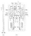
図1は、本発明の検査システムに用いられる検査装置80の外観図である。
FIG. 1 is an external view of an
検査装置80はマイクロチップ1に予め注入された検体と、試薬との反応を自動的に検出し、表示部84に結果を表示する装置である。
The
マイクロチップ1をチップ搬送トレイ2に載置した後チップ搬送トレイ2を挿入口83にローディングし、筐体82の内部にセットするようになっている。85はメモリカードスロット、86はプリント出力口、87は操作パネル、88は入出力端子、89はトレイ蓋、91は排出ボタンである。
After the
図1(a)はチップ搬送トレイ2がマイクロチップ1を載置可能な位置に排出された状態の外観図、図1(b)はチップ搬送トレイ2が検査可能な位置にローディングされた状態の外観図である。
FIG. 1A is an external view of a state where the
検査担当者はマイクロチップ1をチップ搬送トレイ2に載置し、排出ボタン91を押してチップ搬送トレイ2を図1(a)の矢印の方向に移動させる。チップ搬送トレイ2が図1(b)のように検査可能な位置まで移動すると、検査担当者は操作パネル87を操作して検査を開始させる。
The person inspecting places the
筐体82の内部では、制御手段の指令により図1には図示せぬマイクロポンプユニット75がマイクロチップ1に駆動液等の液体を注入し、マイクロチップ1内の反応の検査が自動的に行われる。検査が終了すると液晶パネルなどで構成される表示部84に結果が表示される。検査結果は操作パネル87の操作により、プリント出力口86よりプリントを出力したり、メモリカードスロット85に挿入されたメモリカードに記憶することができる。また、外部入出力端子88から例えばLANケーブルを使って、パソコンなどにデータを保存することができる。
In the
検査担当者は、検査終了後、排出ボタン91を押してチップ搬送トレイ2を図1(a)のようにマイクロチップ1を取り出し可能な位置まで移動させる。検査担当者は、マイクロチップ1をチップ搬送トレイ2から取り出す。
After the inspection is completed, the person inspecting presses the
なお、本実施形態ではモータ等の駆動手段によりチップ搬送トレイ2を移動させる例を説明するが、特に本発明の適用を限定されるものではなく手動でチップ搬送トレイ2を移動させても良い。
In this embodiment, an example in which the
図2は本発明の実施形態に係るマイクロチップ1の一例の外観図である。
FIG. 2 is an external view of an example of the
図2(a)のマイクロチップ1の側面図に示すように、マイクロチップ1は溝形成基板108と、溝形成基板108を覆う被覆基板109から構成されている。図2(a)の矢印は、検査装置80にマイクロチップ1を挿入する挿入方向である。
As shown in the side view of the
図2(b)はマイクロチップ1の平面図であり、透明な被覆基板109を通して見える溝形成基板108の溝を図示している。溝形成基板108の溝を被覆基板109が覆うことにより流路を形成している。マイクロチップ1には、検査、試料の処理などを行うための、微小な溝状の流路250(微細流路)および機能部品(流路エレメント)が、用途に応じた適当な態様で配設されている。
FIG. 2B is a plan view of the
流路はマイクロメーターオーダーで形成されており、例えば幅は数μm〜数百μm、好ましくは10〜200μmで、深さは25〜500μm程度、好ましくは25〜250μmである。 The flow path is formed on the order of micrometers, and for example, the width is several μm to several hundred μm, preferably 10 to 200 μm, and the depth is about 25 to 500 μm, preferably 25 to 250 μm.
本実施形態では、特定の遺伝子の増幅およびその検出を行う処理に用いるマイクロチップ1を例に説明する。
In the present embodiment, a
図2(b)の110a、110b、110cはマイクロチップ1内部の流路に連通する駆動液注入部であり、各駆動液注入部110から駆動液を注入し内部の検体や試薬等を駆動する。113はマイクロチップ1に検体を注入するための検体注入部であり、注射器などを用いて検体注入部113から血液などの検体を注入する。
2B,
本実施形態のマイクロチップ1では検体注入部113の下流の流路250は2方向に分岐し、検体を2分割するように構成されている。駆動液注入部110bから駆動液を注入すると、検体注入部113に注入されている検体は、検体注入部113と連通する流路250aaと流路250abを通ってそれぞれ検体収容部121a、121bに収容される。検体収容部121a、121bは所定量の検体を収容するために他の流路より溝が深くなっている。
In the
検体収容部121a、121bの溝の深さは例えば1.5μm、液溜部140a、140bの溝の深さは例えば1μm、他の流路の溝の深さは例えば0.25μmである。
The depth of the grooves of the
120a、120bは試薬類を収容する試薬収容部である。駆動液注入部110a、110cから駆動液を注入すると、試薬収容部120a、120bに収容された試薬は流路250に押し出されて、それぞれ下流の検体収容部121a、121bに注入される。検体と試薬が混合された液体は、流路250caと流路250cbを通ってそれぞれ下流の検出部19a、19bに収容される。
120a and 120b are reagent storage units for storing reagents. When the driving liquid is injected from the driving
検査装置80の内部で検出部19a、19bを加熱または吸熱して所定の温度で検体と試薬とを所定の時間反応させる。
The
検出部19a、19bは検体と試薬の反応を光学的に検出するために設けられ、所定量の検体と試薬を収容するために他の流路より溝が深くなっている。
The
検出部19a、19bの溝の深さは例えば1.5μm、他の流路の溝の深さは0.25μmである。検出部19a、19bに光を照射すると、検体と反応した試薬が例えば蛍光を発光するので蛍光の光量を測定することにより反応結果を計測する。
The depth of the grooves of the
次に、マイクロチップ1を構成する溝形成基板108と被覆基板109に用いる材料について説明する。
Next, materials used for the
マイクロチップ1は、加工成形性、非吸水性、耐薬品性、耐候性、コストなどに優れていることが望まれており、マイクロチップ1の構造、用途、検出方法などを考慮して、マイクロチップ1の材料を選択する。その材料としては従来公知の様々なものが使用可能であり、個々の材料特性に応じて通常は1以上の材料を適宜組み合わせて、基板および流路エレメントが成形される。
The
特に、多数の測定検体、とりわけ汚染、感染のリスクのある臨床検体を対象とするチップは、ディスポーサブルタイプであることが望ましい。そのため、量産可能であり、軽量で衝撃に強く、焼却廃棄が容易なプラステック樹脂、例えば、透明性、機械的特性および成型性に優れて微細加工がしやすいポリスチレンが好ましい。また、例えば分析においてチップを100℃近くまで加熱する必要がある場合には、耐熱性に優れる樹脂(例えばポリカーボネートなど)を用いることが好ましい。また、タンパク質の吸着が問題となる場合にはポリプロピレンを用いることが好ましい。樹脂やガラスなどは熱伝導率が小さく、マイクロチップの局所的に加熱される領域に、これらの材料を用いることにより、面方向への熱伝導が抑制され、加熱領域のみ選択的に加熱することができる。 In particular, it is desirable that a chip intended for a large number of measurement specimens, particularly clinical specimens at risk of contamination and infection, be of a disposable type. Therefore, a plastic resin that can be mass-produced, is lightweight, is strong against impact, and can be easily disposed of by incineration, for example, polystyrene that is excellent in transparency, mechanical properties, and moldability and is easy to be finely processed is preferable. For example, when it is necessary to heat the chip to near 100 ° C. in analysis, it is preferable to use a resin having excellent heat resistance (for example, polycarbonate). In addition, when protein adsorption becomes a problem, it is preferable to use polypropylene. Resin and glass have low thermal conductivity, and by using these materials in the locally heated region of the microchip, heat conduction in the surface direction is suppressed, and only the heated region is selectively heated. Can do.
検出部19において、呈色反応の生成物や蛍光物質などの検出を光学的に行うので、少なくとも被覆基板109のこの部位は光透過性の材料(例えばアルカリガラス、石英ガラス、透明プラスチック類)を用い、光が透過するようにする必要がある。
Since the detection unit 19 optically detects a color reaction product or a fluorescent substance, at least this portion of the
図3は、検査装置80の内部構成を説明するための斜視図である。なお、図3では説明を簡単にするためチップ搬送トレイ2を図示していない。
FIG. 3 is a perspective view for explaining the internal configuration of the
検査装置80は、温度調節ユニット152、検出ユニット15、駆動液ポンプ92、パッキン90、駆動液タンク91、送りネジ301、ジョイント302、モータ300などから構成される。図3のようにマイクロチップ1の面を温度調節ユニット152が密着している。また、図3はマイクロチップ1をパッキン90bに密着させている状態を示している。
The
以下、図3を用いて検査装置80の内部構成の例を説明する。
Hereinafter, an example of the internal configuration of the
温度調節ユニット152とマイクロチップ1は、図示せぬ駆動部材により駆動され、紙面上下方向に移動可能である。初期状態において、駆動部材により温度調節ユニット152を、図3の状態からマイクロチップ1の厚み以上上昇させる。すると、マイクロチップ1は図3の矢印A方向に挿抜可能であり、チップ搬送トレイ2に載置されたマイクロチップ1は、フォトインタラプタなどを用いたチップ検知部95がマイクロチップ1を検知する所定の位置まで図示せぬ駆動部材により搬送される。
The
温度調節ユニット152は、ペルチェ素子、電源装置、温度制御装置などを内蔵し、発熱または吸熱を行ってマイクロチップ1の面を所定の温度に調整するユニットである。
The
次に、駆動部材により温度調節ユニット152とチップ搬送トレイ2に載置されたマイクロチップ1を下降させて、マイクロチップ1を温度調節ユニット152とパッキン90bに密着させる。
Next, the
マイクロチップ1の検出部19では、検体と前記マイクロチップ1内に貯蔵された蛍光物質を含む試薬が反応し、励起光を照射すると蛍光をおこす。本実施形態では検出部19でおこる試薬の反応結果を光学的に検出する。
In the detection unit 19 of the
図3に示すマイクロチップ1の例は、被覆基板109にバーコード25が設けられており、試薬の反応結果を測光する検出部19がマイクロチップ1の内部に2つ設けられている。
In the example of the
2つの検出部19a、19bは、図3に示す直線Fに沿って配設されている。検出部19a、19bの位置に対応する被覆基板109の面には透明な窓がそれぞれ設けられており、窓を介して反応結果を光学的に検出できる。
The two
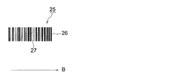
図4はバーコード25の一例を説明するための平面図である。バーコード25は棒状の黒バー26と白バー27からなる1次元バーコードであり、黒バー26と白バー27と直交する矢印Bの方向に黒バー26と白バー27の間隔をそれぞれ読みとることにより符号化された情報を読みとることができる。図3に示すマイクロチップ1では、黒バー26および白バー27と直交する矢印Bの方向が矢印Fと平行になるようにバーコード25が設けられている。
FIG. 4 is a plan view for explaining an example of the
図3に戻って説明を続ける。検出ユニット15は、送りネジ301と螺合するネジ部を有し、送りネジ301が回転することにより図3の矢印B方向または逆方向に移動する。送りネジ301は直線Fと平行に配設されており、検出ユニット15が送りネジ301によって移動すると、バーコード25から黒バー26または白バー27からの反射光を受光できる位置に検出ユニット15の図示せぬ第1受光部181の光軸が一致するように配置されている。第1受光部181は本発明の第1の受光部である。
Returning to FIG. 3, the description will be continued. The
また、検出部19a、19bのそれぞれの中心部に、検出ユニット15の図示せぬ第2受光部161の光軸が一致するように配置されている。検出ユニット15は、所定の位置に移動した後、検出部19a、19bに順次励起光を照射し、蛍光物質が発光する蛍光を受光して電気信号を出力する。
Moreover, it arrange | positions so that the optical axis of the 2nd light-receiving part 161 (not shown) of the
送りネジ301はモータ300によりジョイント302を介して駆動される。モータ300は例えばパルスモータであり、パルスにより所定量回転する。モータ300は本発明の検出ユニット駆動手段である。第1位置検出部40、第2位置検出部41は検出ユニット15の待機位置と初期位置とを検出するために設けられた、例えば光学センサやホールセンサなどの位置検出センサである。
The
なお、検出ユニット15には回転防止用にガイド穴が設けられており、ガイド穴を貫通するガイド棒310に沿って移動する。ガイド棒310は送りネジ301と平行に配設されている。
The
また、本実施形態ではマイクロチップ1に検出部19が2つ設けられている場合について説明したが、検出部19の数は1つ以上であればいくつでも良い。
In the present embodiment, the case where two detection units 19 are provided in the
駆動液ポンプ92の吸込側には、パッキン90cが接続され、駆動液タンク91に充填された駆動液を吸い込むようになっている。一方、駆動液ポンプ92の吐出側にはパッキン90bが接続されていて、パッキン90cから吸い込んだ駆動液を、パッキン90bを介してマイクロチップ1の駆動液注入部110からマイクロチップ1内に形成された流路250に注入する。パッキン90bは駆動液ポンプ92とマイクロチップ1の間に挟まれ、駆動液ポンプ92の駆動液出口とパッキン90bの開口部と駆動液注入部110とは連通している。このように、駆動液ポンプ92から、連通しているパッキン90bを介して駆動液注入部110より駆動液を注入する。
A
次に、第1の実施形態の検査システムに用いられる検出ユニット15の詳細について図5、図6、図7を用いて説明する。
Next, details of the
図5は、第1の実施形態の検査システムに用いられるマイクロチップ1と検出ユニット15の詳細を説明するための斜視図である。図5は、図3に図示した検査装置80の内部機構の一部を別の角度から図示したものであり、図3には図示しなかったチップ搬送トレイ2も図示している。今までに説明した構成要素には同番号を付し説明を省略する。
FIG. 5 is a perspective view for explaining details of the
検出ユニット15のマイクロチップ1と対向する面にはレンズ190、レンズ155が設けられている。レンズ190は、バーコード25の黒バー26からの光または白バー27からの光を第1受光部181に集光する光学系の集光レンズである。また、レンズ155は検出部19aまたは検出部19bから反応結果の光を第2受光部161に集光する光学系の集光レンズである。
A
第1の実施形態ではこのように検出ユニット15に第1受光部181と、第1受光部181に集光する光学系、第2受光部161と、第2受光部161に集光する光学系がそれぞれ設けられている。
In the first embodiment, the first
図6は、検出ユニット15のバーコード25の黒バー26からの光または白バー27からの光を第1受光部181に集光する光学系の一例を説明するための断面図である。図6に示す断面は、検出ユニット15をレンズ190の光軸L1を通るように矢印B方向に切断した断面である。
FIG. 6 is a cross-sectional view for explaining an example of an optical system that collects light from the
バーコード25の黒バー26からの光または白バー27からの光を第1受光部181に集光する光学系は、例えばレンズ190、レンズ168、ダイクロイックミラー191、レンズ169、第1発光部180、第1受光部181、基板163、164などから構成される。
The optical system that focuses the light from the
第1発光部180から照射される光は、ダイクロイックミラー191で反射し、バーコード25を照明する。黒バー26または白バー27で反射した光は、ダイクロイックミラー191を透過してレンズ169を介して第1受光部181に入射する。
The light emitted from the first
図7は、検出部19から反応結果の光を受光する第2の受光部を第2受光部161に集光する光学系の一例を説明するための断面図である。図7に示す断面は、検出ユニット15をレンズ155の光軸L2を通るように矢印B方向に切断した断面である。
FIG. 7 is a cross-sectional view for explaining an example of an optical system that condenses the second light receiving unit that receives the light of the reaction result from the detection unit 19 on the second
検出部19から反応結果の光を第2受光部161に集光する光学系は、例えばレンズ155、レンズ268、ダイクロイックミラー261、レンズ269、励起光カットフィルタ156、第2発光部160、第2受光部161、基板263、264などから構成される。励起光カットフィルタ156は、ダイクロイックミラー261に蒸着されていて、検出部19で発生する蛍光の波長を選択的に第2受光部161の方向に透過する。
The optical system that condenses the reaction result light from the detection unit 19 on the second
第2発光部160から照射される光は、ダイクロイックミラー261で反射し、検出部19を照射する。検出部19で発生する蛍光は、励起光カットフィルタ156を介してダイクロイックミラー261を透過して第2受光部161に入射する。ダイクロイックミラー261を透過した光には励起光が多く含まれているので、ダイクロイックミラー261に設けた励起光カットフィルタ156により励起光をカットし、蛍光のみを第2受光部161に入射するようにしている。
The light emitted from the second
蛍光物質を励起する励起光と、蛍光の波長の差は数nm〜数10nmと非常に少ないため、励起光カットフィルタ156は、励起光と蛍光を分離するために急峻な遮断特性を持つ必要がある。
Since the difference in wavelength between the excitation light for exciting the fluorescent substance and the fluorescence is very small, from several nanometers to several tens of nanometers, the excitation light cut
図8は、本発明の第1の実施形態における検査装置80の回路ブロック図である。
FIG. 8 is a circuit block diagram of the
制御部99は、CPU98(中央処理装置)とRAM97(Random Access Memory)、ROM96(Read Only Memory)等から構成され、不揮発性の記憶部であるROM96に記憶されているプログラムをRAM97に読み出し、当該プログラムに従って検査装置80の各部を集中制御する。
The
以下、いままでに説明した機能と同一機能を有する機能ブロックには同番号を付し、説明を省略する。 Hereinafter, functional blocks having the same functions as those described so far are denoted by the same reference numerals, and description thereof is omitted.
チップ検知部95はマイクロチップ1が規制部材に当接すると検知信号をCPU98に送信する。CPU98は検知信号を受信すると、機構駆動部32に指令し所定の手順でマイクロチップ1を下降または上昇させる。
The
ポンプ駆動部500は各マイクロポンプの圧電素子を駆動する駆動部である。ポンプ駆動制御部412はプログラムに基づいて、所定量の駆動液を注入または吸入するようにポンプ駆動部500を制御する。ポンプ駆動部500はポンプ駆動制御部412の指令を受けて、圧電素子を駆動する。
The
CPU98は所定のシーケンスで検査を行い、検査結果をRAM97に記憶する。検出ユニット駆動制御部411はモータ300を所定量回転させて、少なくともバーコード25に黒バー26、白バー27が記されている区間、検出ユニット15を移動させる。また、モータ300を所定量回転させて、所定の検出部19を検査する位置まで検出ユニット15を移動させる。バーコード読み取り部409は、第1の受光部181が出力する電気信号からバーコード読み取り、バーコード情報を解読する。光量算出部410は、第2受光部161の出力する電気信号から蛍光の光量を算出し検査結果とする。
The
検査結果は、操作部87の操作によりメモリカード501に記憶したり、プリンタ503によってプリントすることができる。
The inspection result can be stored in the
図9は本発明の第1の実施形態の検査システムによる検査の手順を説明するフローチャートである。 FIG. 9 is a flowchart for explaining an inspection procedure by the inspection system according to the first embodiment of the present invention.
なお、温度調節ユニット152は検査装置80の電源投入時に通電され、所定の温度になっているものとする。また、検査に先立って、パッキン90b上端まで駆動液11が充填されているものとする。
It is assumed that the
検査担当者は、最初に挿入口83からマイクロチップ1をチップ搬送トレイ2に載置し、排出ボタン91を押してチップ搬送トレイ2を検査可能な位置まで移動させ検査を開始させる。すると、CPU98がチップ検知部95から検知信号を検知して、機構駆動部32を制御し、図3のようにパッキン90bと温度調節ユニット152がマイクロチップ1に密着する。
The person inspecting first places the
本実施形態では、この状態からポンプ駆動制御部412が駆動液を各駆動液注入部110から所定の手順で注入し、マイクロチップ1内部の流路で所定の反応を行った後、試薬等と反応させた検体が検出部19a、19bに注入され反応結果を検出可能な状態になっているものとする。
In this embodiment, from this state, the pump
この状態からCPU98が検査のために行う手順について説明する。本実施形態では図3に示すマイクロチップ1のように複数の検出部19が一列に並んでいるものとする。
A procedure performed by the
S101:測定回数をn=0とする。 S101: The number of measurements is set to n = 0.
CPU98は、測定回数をn=0とする。
The
S102:検出ユニット15の位置を初期化するステップである。
S102: This is a step of initializing the position of the
検出ユニット駆動制御部411は、検出ユニット15が図3の矢印Bと反対方向に移動するようモータ300を回転させるとともに、第1位置検知部40の状態を検知する。検出ユニット15が第1位置検知部40に当接し、第1位置検知部40の備えるスイッチがオンになると検出ユニット駆動制御部411はモータ300の回転を停止する。
The detection unit
S103:検出ユニット15を所定量移動させる。
S103: The
検出ユニット駆動制御部411は、少なくともバーコード25の黒バー26、白バー27が記されている区間を光軸L1が一定速度で通過するように、検出ユニット15を駆動する。
The detection unit
S104:バーコードを読みとるステップである。 S104: This is a step of reading a barcode.
バーコード読み取り部409は、第1受光部181から出力される光量に比例した電気信号のデータを順次RAM97に記憶させる。バーコード読み取り部409は、バーコード25の読み取り終了後、RAM97に記憶されているデータを復号し、マイクロチップ1に関する情報を取得する。
The bar
S106:検出ユニット15を所定量移動させる。
S106: The
検出ユニット駆動制御部411は、これから測定する検出部19の中心に略一致する位置に光軸L2が移動するまで所定のパルスをモータ300に与えて移動させる。
The detection unit
S107:光量を測定するステップである。 S107: This is a step of measuring the amount of light.
光量算出部410は、第2発光部160に発光を指令し、第2受光部161から出力される光量に比例した電気信号のデータをRAM97に一時記憶する。
The light
S108:n=n+1とする。 S108: n = n + 1.
CPU98は、測定回数をn=n+1とする。
The
S109:n=Nか、否か、を判定するステップである。 S109: This is a step of determining whether or not n = N.
CPU98は、測定回数が所定の回数Nか、否かを判定する。例えば、検出部19の数が2つの場合はN=2である。
The
n=Nではない場合、(ステップS109;No)、ステップS106に戻る。 If n = N is not satisfied (step S109; No), the process returns to step S106.
n=Nの場合、(ステップS109;Yes)、ステップS110に進む。 When n = N (step S109; Yes), the process proceeds to step S110.
S110:待機位置に検出ユニット15を移動させるステップである。
S110: This is a step of moving the
検出ユニット駆動制御部411は、所定の数のパルスを与えてモータ300を回転させ、所定の位置に停止させる。
The detection
以上で、マイクロチップ1のバーコード読み取りと光量測定の手順は終了である。
This completes the procedure for reading the barcode of the
このように本発明では、バーコード読み取りと光量測定を同じ機構で行えるので、機構が簡単になり検査システムを小型化できる。 Thus, in the present invention, since the barcode reading and the light quantity measurement can be performed by the same mechanism, the mechanism is simplified and the inspection system can be downsized.
次に、第2の実施形態の検査システムに用いられる検出ユニット15の詳細について図10、図11、図12を用いて説明する。
Next, details of the
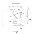
図10は、第2の実施形態の検査システムに用いられるマイクロチップ1と検出ユニット15の詳細を説明するための斜視図である。
FIG. 10 is a perspective view for explaining details of the
第2の実施形態では検出ユニット15に第2受光部161を設けず、第1受光部181が反応結果の光も受光する。そのため、バーコード25と2つの検出部19a、19bは、図10に示すよう直線Gに沿ってマイクロチップ1に配設されている。また、検出ユニット15のマイクロチップ1と対向する面には第1受光部181に集光するレンズ190だけ設けられている。直線Gは、黒バー26、白バー27と直交し、矢印Bと平行である。
In the second embodiment, the second
図11、図12は、第2の実施形態の第1受光部181に集光する光学系の一例を説明するための断面図である。図11、図12に示す断面は、検出ユニット15をレンズ190の光軸L1を通るように矢印B方向に切断した断面である。
11 and 12 are cross-sectional views for explaining an example of an optical system that focuses light on the first
図6で説明した光学系とほとんど同じ構成であるが、一部分に励起光カットフィルタ156が蒸着されたダイクロイックミラー193を用いて、ダイクロイックミラー193を軸170を中心に回転させることにより光路中に励起光カットフィルタ156を挿抜可能に構成されている。フィルタ駆動部280は、ベルトなどにより軸170と連結し、ダイクロイックミラー193を回転させて励起光カットフィルタ156を図12のように光路中に挿入する。励起光カットフィルタ156は本発明の反応結果の光を選択的に透過するフィルタ、フィルタ駆動部280は本発明のフィルタ駆動手段である。
The optical system has almost the same configuration as the optical system described in FIG. 6, but is excited in the optical path by rotating the
なお、本実施形態ではダイクロイックミラー193の一部に励起光カットフィルタ156を蒸着し、ダイクロイックミラー193を回転させて励起光カットフィルタ156を挿抜する例を説明するが、この例に限らず別部材の励起光カットフィルタ156を光路中に挿抜しても良い。
In the present embodiment, an example in which the excitation light cut
図11は、励起光カットフィルタ156が光路中に挿入されていない状態であり、バーコード25を読みとるときに用いる。第1受光部181に集光する光学系は、例えばレンズ190、レンズ168、ダイクロイックミラー193、レンズ169、第1発光部180、第1受光部181、基板163、164などから構成される。
FIG. 11 shows a state in which the excitation light cut
第1発光部180から照射される光は、ダイクロイックミラー193で反射し、バーコード25を照明する。黒バー26または白バー27で反射した光は、レンズ190で集光され、ダイクロイックミラー193を透過してレンズ169を介して第1受光部181に入射する。
The light emitted from the first
図12は、励起光カットフィルタ156が光路中に挿入された状態であり、反応結果を検出するときに用いる。
FIG. 12 shows a state in which the excitation light cut
第1発光部180から照射される光は、ダイクロイックミラー193で反射し、検出部19を照射する。検出部19で発生する蛍光は、レンズ190で集光され、励起光カットフィルタ156を介してダイクロイックミラー193を透過して第1受光部181に入射する。
The light emitted from the first
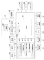
図13は、本発明の第2の実施形態における検査装置80の回路ブロック図である。
FIG. 13 is a circuit block diagram of the
第1の実施形態のブロック図との違いは、検出ユニット15にフィルタ駆動部280が設けられ、CPU98にフィルタ駆動部280を制御するフィルタ駆動制御部413が設けられている点である。また、第2発光部160、第2受光部161は設けられていない。その他は第1の実施形態と同様であり説明を省略する。
The difference from the block diagram of the first embodiment is that a
図14は本発明の第2の実施形態の検査システムによる検査の手順を説明するフローチャートである。 FIG. 14 is a flowchart for explaining an inspection procedure by the inspection system according to the second embodiment of the present invention.
図9で説明した状態からCPU98が検査のために行う手順について説明する。本実施形態では図10に示すマイクロチップ1のようにバーコード25と複数の検出部19が一列に並んでいるものとする。
A procedure performed by the
S201:測定回数をn=0とする。 S201: The number of measurements is set to n = 0.
CPU98は、測定回数をn=0とする。
The
S202:検出ユニット15の位置を初期化するステップである。
S202: This is a step of initializing the position of the
検出ユニット駆動制御部411は、検出ユニット15が図3の矢印Bと反対方向に移動するようモータ300を回転させるとともに、第1位置検知部40の状態を検知する。検出ユニット15が第1位置検知部40に当接し、第1位置検知部40の備えるスイッチがオンになると検出ユニット駆動制御部411はモータ300の回転を停止する。
The detection unit
S203:検出ユニット15を所定量移動させる。
S203: Move the
検出ユニット駆動制御部411は、少なくともバーコード25の黒バー26、白バー27が記されている区間を光軸L1が一定速度で通過するように、検出ユニット15を駆動する。
The detection unit
S204:バーコードを読みとるステップである。 S204: A step of reading a barcode.
バーコード読み取り部409は、第1受光部181から出力される光量に比例した電気信号のデータを順次RAM97に記憶させる。バーコード読み取り部409は、バーコード25の読み取り終了後、RAM97に記憶されているデータを復号し、マイクロチップ1に関する情報を取得する。
The bar
S205:フィルタを挿入するステップである。 S205: This is a step of inserting a filter.
フィルタ駆動制御部413は、フィルタ駆動部280を制御し励起光カットフィルタ156が光路中に挿入されるまでダイクロイックミラー193を回転させる。
The filter
S206:検出ユニット15を所定量移動させる。
S206: The
検出ユニット駆動制御部411は、これから測定する検出部19の中心に光軸L1が略一致する位置に移動するまで所定のパルスをモータ300に与えて移動させる。
The detection unit
S207:光量を測定するステップである。 S207: This is a step of measuring the amount of light.
光量算出部410は、第1発光部180に発光を指令し、第1受光部181から出力される光量に比例した電気信号のデータをRAM97に一時記憶する。
The light
S208:n=n+1とする。 S208: n = n + 1.
CPU98は、測定回数をn=n+1とする。
The
S209:n=Nか、否か、を判定するステップである。 S209: It is a step of determining whether n = N or not.
CPU98は、測定回数が所定の回数Nか、否かを判定する。例えば、検出部19の数が2つの場合はN=2である。
The
n=Nではない場合、(ステップS109;No)、ステップS206に戻る。 If n = N is not satisfied (step S109; No), the process returns to step S206.
n=Nの場合、(ステップS109;Yes)、ステップS210に進む。 When n = N (step S109; Yes), the process proceeds to step S210.
S210:待機位置に検出ユニット15を移動させるステップである。
S210: This is a step of moving the
検出ユニット駆動制御部411は、所定の数のパルスを与えてモータ300を回転させ、所定の位置に停止させる。
The detection
以上で、マイクロチップ1のバーコード読み取りと光量測定の手順は終了である。
This completes the procedure for reading the barcode of the
このように第2の実施形態では、バーコード読み取りと光量測定を同じ受光部で受光するので、機構が簡単になり検査システムを小型化できる。 As described above, in the second embodiment, since the barcode reading and the light amount measurement are received by the same light receiving unit, the mechanism is simplified and the inspection system can be downsized.
以上このように、本発明によれば、簡単な構成でマイクロチップに設けられたバーコードを読みとることができる小型の検査システムを提供することができる。 As described above, according to the present invention, it is possible to provide a small inspection system capable of reading a barcode provided on a microchip with a simple configuration.
1 マイクロチップ
15 検出ユニット
19 検出部
25 バーコード
26 黒バー
27 白バー
80 検査装置
82 筐体
83 挿入口
84 表示部
87 操作ボタン
90 パッキン
92 駆動液ポンプ
110 駆動液注入口
113 検体注入部
121 検体収容部
152 温度調整ユニット
156 励起光カットフィルタ
160 第2発光部
161 第2受光部
180 第1発光部
181 第1受光部
191 ダイクロイックミラー
193 ダイクロイックミラー
250 流路
261 ダイクロイックミラー
280 フィルタ駆動部
300 モータ
301 送りネジ
302 ジョイント
413 フィルタ駆動制御部
DESCRIPTION OF
Claims (6)
前記マイクロチップに設けられた黒バーと白バーとからなるバーコードと、
前記黒バーからの光または前記白バーからの光を受光し電気信号に変換する第1の受光部と、
前記第1の受光部を備えた検出ユニットと、
前記検出ユニットを前記黒バーおよび前記白バーと直交する方向に移動させる検出ユニット駆動手段と、
を有することを特徴とする検査システム。 In the inspection system that optically detects and measures the reaction result from the detection part of the microchip,
A barcode consisting of a black bar and a white bar provided on the microchip;
A first light receiving unit that receives light from the black bar or light from the white bar and converts the light into an electrical signal;
A detection unit including the first light receiving unit;
Detection unit driving means for moving the detection unit in a direction perpendicular to the black bar and the white bar;
An inspection system comprising:
前記検出部からの光を受光する第2の受光部を備えることを特徴とする請求項1に記載の検査システム。 The detection unit is
The inspection system according to claim 1, further comprising a second light receiving unit that receives light from the detection unit.
前記検出ユニット駆動手段によって前記検出ユニットが移動すると、前記検出部からの光を前記第2の受光部が受光できる位置に配置されていることを特徴とする請求項2に記載の検査システム。 The detection unit and the second light receiving unit are:
3. The inspection system according to claim 2, wherein when the detection unit is moved by the detection unit driving unit, the inspection unit is disposed at a position where the second light receiving unit can receive light from the detection unit.
前記検出ユニット駆動手段によって前記検出ユニットが移動すると、前記検出部からの光を前記第1の受光部が受光できる位置に配置されていることを特徴とする請求項1に記載の検査システム。 The detection unit and the first light receiving unit are:
The inspection system according to claim 1, wherein when the detection unit is moved by the detection unit driving unit, the inspection unit is arranged at a position where the light from the detection unit can be received by the first light receiving unit.
前記黒バーからの光または前記白バーからの光を前記第1の受光部に集光する光学系と、
前記反応結果の光を選択的に透過するフィルタと、
前記フィルタを前記光学系の光路中に挿抜するフィルタ駆動手段と、
を有することを特徴とする請求項4に記載の検査システム。 The detection unit is
An optical system for condensing the light from the black bar or the light from the white bar on the first light receiving unit;
A filter that selectively transmits light of the reaction result;
Filter driving means for inserting and removing the filter in the optical path of the optical system;
The inspection system according to claim 4, further comprising:
前記制御手段は、
前記第1の受光部が前記バーコードからの光を受光する位置では前記フィルタを前記光路中から退避させ、前記第1の受光部が前記反応結果の光を受光する位置では前記フィルタを前記光路中に挿入するように制御することを特徴とする請求項5に記載の検査システム。 Control means for controlling the detection unit driving means and the filter driving means;
The control means includes
The filter is retracted from the optical path at a position where the first light receiving unit receives light from the barcode, and the filter is moved to the optical path at a position where the first light receiving unit receives light of the reaction result. 6. The inspection system according to claim 5, wherein the inspection system is controlled to be inserted therein.
Priority Applications (1)
| Application Number | Priority Date | Filing Date | Title |
|---|---|---|---|
| JP2008075504A JP2009229263A (en) | 2008-03-24 | 2008-03-24 | Inspection system |
Applications Claiming Priority (1)
| Application Number | Priority Date | Filing Date | Title |
|---|---|---|---|
| JP2008075504A JP2009229263A (en) | 2008-03-24 | 2008-03-24 | Inspection system |
Publications (1)
| Publication Number | Publication Date |
|---|---|
| JP2009229263A true JP2009229263A (en) | 2009-10-08 |
Family
ID=41244834
Family Applications (1)
| Application Number | Title | Priority Date | Filing Date |
|---|---|---|---|
| JP2008075504A Pending JP2009229263A (en) | 2008-03-24 | 2008-03-24 | Inspection system |
Country Status (1)
| Country | Link |
|---|---|
| JP (1) | JP2009229263A (en) |
Cited By (1)
| Publication number | Priority date | Publication date | Assignee | Title |
|---|---|---|---|---|
| JP2013525763A (en) * | 2010-04-16 | 2013-06-20 | オプコ・ダイアグノスティクス・リミテッド・ライアビリティ・カンパニー | System and device for sample analysis |
-
2008
- 2008-03-24 JP JP2008075504A patent/JP2009229263A/en active Pending
Cited By (5)
| Publication number | Priority date | Publication date | Assignee | Title |
|---|---|---|---|---|
| JP2013525763A (en) * | 2010-04-16 | 2013-06-20 | オプコ・ダイアグノスティクス・リミテッド・ライアビリティ・カンパニー | System and device for sample analysis |
| US9643182B2 (en) | 2010-04-16 | 2017-05-09 | Opko Diagnostics, Llc | Systems and devices for analysis of samples |
| US9682376B2 (en) | 2010-04-16 | 2017-06-20 | Opko Diagnostics, Llc | Systems and devices for analysis of samples |
| US10456784B2 (en) | 2010-04-16 | 2019-10-29 | Opko Diagnostics, Llc | Systems and devices for analysis of samples |
| US11458473B2 (en) | 2010-04-16 | 2022-10-04 | Opko Diagnostics, Llc | Systems and devices for analysis of samples |
Similar Documents
| Publication | Publication Date | Title |
|---|---|---|
| US9081001B2 (en) | Diagnostic systems and instruments | |
| JP4943445B2 (en) | Method and system for delivering a fluid sample to a sensor array | |
| JP2009019962A (en) | Fluorescence detection unit, reaction detection device, and microchip inspection system | |
| JP6238207B2 (en) | Optical analysis method, optical analysis system and program | |
| JP6197263B2 (en) | Microchip | |
| JPH10221245A (en) | Miniaturized sensor using optics furnished with integrated hydrodynamic system | |
| US9517466B2 (en) | Measuring cassette and measuring device for the detection of target molecules in a liquid sample by measurement of fluorescence emission after excitation in an evanescent field | |
| WO2009125676A1 (en) | Inspection system | |
| JP4985646B2 (en) | Reaction vessel kit | |
| JP2008128869A (en) | Microchip inspection system and program used for the microchip inspection system | |
| JP2009042103A (en) | Base, reaction processor using it and reaction control method | |
| US20130156642A1 (en) | Optical detection system, a cartridge therefor and a reader therefor | |
| JP2009229263A (en) | Inspection system | |
| JP2009058256A (en) | Fluorescence detection unit, reaction detector and microchip inspection system | |
| JP2008128706A (en) | Microchip inspection system and program used for the microchip inspection system | |
| JP2009103641A (en) | Inspection apparatus | |
| JP2009300256A (en) | Inspecting system | |
| JP2009097999A (en) | Inspection apparatus | |
| JP2009058352A (en) | Inspection apparatus | |
| JP2009128277A (en) | Inspection apparatus and inspection system | |
| JP2009092455A (en) | Inspecting device | |
| JP2009122021A (en) | Inspection system | |
| WO2009113356A1 (en) | Reaction detection device | |
| JP2009229264A (en) | Inspection system | |
| JP2009025014A (en) | Reaction detection device and microchip inspection system |