JP2009191340A - Film-forming apparatus and film-forming method - Google Patents
Film-forming apparatus and film-forming method Download PDFInfo
- Publication number
- JP2009191340A JP2009191340A JP2008035643A JP2008035643A JP2009191340A JP 2009191340 A JP2009191340 A JP 2009191340A JP 2008035643 A JP2008035643 A JP 2008035643A JP 2008035643 A JP2008035643 A JP 2008035643A JP 2009191340 A JP2009191340 A JP 2009191340A
- Authority
- JP
- Japan
- Prior art keywords
- metal target
- film forming
- frame member
- metal
- forming apparatus
- Prior art date
- Legal status (The legal status is an assumption and is not a legal conclusion. Google has not performed a legal analysis and makes no representation as to the accuracy of the status listed.)
- Withdrawn
Links
Images


Classifications
-
- C—CHEMISTRY; METALLURGY
- C23—COATING METALLIC MATERIAL; COATING MATERIAL WITH METALLIC MATERIAL; CHEMICAL SURFACE TREATMENT; DIFFUSION TREATMENT OF METALLIC MATERIAL; COATING BY VACUUM EVAPORATION, BY SPUTTERING, BY ION IMPLANTATION OR BY CHEMICAL VAPOUR DEPOSITION, IN GENERAL; INHIBITING CORROSION OF METALLIC MATERIAL OR INCRUSTATION IN GENERAL
- C23C—COATING METALLIC MATERIAL; COATING MATERIAL WITH METALLIC MATERIAL; SURFACE TREATMENT OF METALLIC MATERIAL BY DIFFUSION INTO THE SURFACE, BY CHEMICAL CONVERSION OR SUBSTITUTION; COATING BY VACUUM EVAPORATION, BY SPUTTERING, BY ION IMPLANTATION OR BY CHEMICAL VAPOUR DEPOSITION, IN GENERAL
- C23C14/00—Coating by vacuum evaporation, by sputtering or by ion implantation of the coating forming material
- C23C14/22—Coating by vacuum evaporation, by sputtering or by ion implantation of the coating forming material characterised by the process of coating
- C23C14/34—Sputtering
- C23C14/35—Sputtering by application of a magnetic field, e.g. magnetron sputtering
-
- C—CHEMISTRY; METALLURGY
- C23—COATING METALLIC MATERIAL; COATING MATERIAL WITH METALLIC MATERIAL; CHEMICAL SURFACE TREATMENT; DIFFUSION TREATMENT OF METALLIC MATERIAL; COATING BY VACUUM EVAPORATION, BY SPUTTERING, BY ION IMPLANTATION OR BY CHEMICAL VAPOUR DEPOSITION, IN GENERAL; INHIBITING CORROSION OF METALLIC MATERIAL OR INCRUSTATION IN GENERAL
- C23C—COATING METALLIC MATERIAL; COATING MATERIAL WITH METALLIC MATERIAL; SURFACE TREATMENT OF METALLIC MATERIAL BY DIFFUSION INTO THE SURFACE, BY CHEMICAL CONVERSION OR SUBSTITUTION; COATING BY VACUUM EVAPORATION, BY SPUTTERING, BY ION IMPLANTATION OR BY CHEMICAL VAPOUR DEPOSITION, IN GENERAL
- C23C14/00—Coating by vacuum evaporation, by sputtering or by ion implantation of the coating forming material
- C23C14/22—Coating by vacuum evaporation, by sputtering or by ion implantation of the coating forming material characterised by the process of coating
- C23C14/34—Sputtering
-
- H—ELECTRICITY
- H01—ELECTRIC ELEMENTS
- H01J—ELECTRIC DISCHARGE TUBES OR DISCHARGE LAMPS
- H01J37/00—Discharge tubes with provision for introducing objects or material to be exposed to the discharge, e.g. for the purpose of examination or processing thereof
- H01J37/32—Gas-filled discharge tubes
- H01J37/34—Gas-filled discharge tubes operating with cathodic sputtering
- H01J37/3402—Gas-filled discharge tubes operating with cathodic sputtering using supplementary magnetic fields
- H01J37/3405—Magnetron sputtering
- H01J37/3408—Planar magnetron sputtering
-
- H—ELECTRICITY
- H01—ELECTRIC ELEMENTS
- H01J—ELECTRIC DISCHARGE TUBES OR DISCHARGE LAMPS
- H01J37/00—Discharge tubes with provision for introducing objects or material to be exposed to the discharge, e.g. for the purpose of examination or processing thereof
- H01J37/32—Gas-filled discharge tubes
- H01J37/34—Gas-filled discharge tubes operating with cathodic sputtering
- H01J37/3411—Constructional aspects of the reactor
- H01J37/3435—Target holders (includes backing plates and endblocks)
Abstract
Description
本発明は、成膜装置及び成膜方法に関するものである。 The present invention relates to a film forming apparatus and a film forming method.
従来の誘電体(SiO2等)の成膜は、高周波スパッタが主流であるが、成膜装置全体の自由度の問題や成膜レートなどの課題により、近年においては、直流反応性スパッタ法が提案されてきている。直流反応性スパッタ法では、ターゲットに金属もしくは導電体を用い、直流電圧により放電を発生させてスパッタリングを行うため、装置全体がシンプルで成膜レートが早いというメリットがある。しかし、チャンバ内に酸素などを導入して気相中や基板表面にてスパッタ粒子を酸化させて誘電体薄膜(酸化膜)を形成するため、金属ターゲットの表面にも酸化膜が形成されやすい。そのため、エロージョンエリア以外のターゲット表面に形成された酸化膜がチャージアップして異常放電が発生するという課題があった。
このような問題を解決する方法として、高周波の重畳やパルス重畳の手法、マグネットを移動してターゲット表面の酸化膜を除去して異常放電を防止する方法が提案されている(例えば、特許文献1,2参照)。
As a method for solving such a problem, a high frequency superposition method or a pulse superposition method, and a method of preventing abnormal discharge by moving the magnet and removing the oxide film on the target surface have been proposed (for example, Patent Document 1). , 2).
しかしながら、この手法においても、エロージョンエリアの外側となるターゲット側面や、シールド板の下に回り込んで酸化膜が形成されることを抑制することができない。特に、「直流反応性スパッタ・対向ターゲット方式」を採用する場合には、シールド板の下のバッキングプレート上における酸化膜の形成が顕著であり、異常放電による放電の不安定要因や、異常放電が原因となるパーティクルの発生が増加して成膜品質が低下するという問題を有する。 However, even with this method, it is not possible to suppress the formation of an oxide film that wraps around the target side surface that is outside the erosion area or under the shield plate. In particular, when the “DC reactive sputtering / opposite target method” is adopted, the formation of an oxide film on the backing plate under the shield plate is remarkable, causing unstable discharge due to abnormal discharge and abnormal discharge. There is a problem in that the generation of particles causing the problem increases and the film formation quality deteriorates.
本発明は、上記従来技術の問題点に鑑み成されたものであって、反応性直流スパッタ放電の安定性を向上させるとともに、パーティクルの発生による欠陥を抑えることのできる成膜装置及び成膜方法を提供することを目的としている。 The present invention has been made in view of the above-described problems of the prior art, and can improve the stability of reactive direct current sputter discharge and can suppress defects caused by generation of particles and a film forming method. The purpose is to provide.
本発明の成膜装置は、上記課題を解決するために、反応性直流型の成膜装置において、
直流電源と、前記直流電源に接続される金属ターゲットと、前記金属ターゲットの外周を取り囲むようにして配置される誘電体枠部材と、前記金属ターゲットの背面側に配置される電極部と、前記金属ターゲット及び前記誘電体枠部材の背面側に配置される磁場発生手段と、を有し、前記磁場発生手段の少なくとも一部が前記誘電体枠部材に沿うように配置されていることを特徴とする。
In order to solve the above problems, a film forming apparatus of the present invention is a reactive DC type film forming apparatus,
A direct current power source, a metal target connected to the direct current power source, a dielectric frame member disposed so as to surround an outer periphery of the metal target, an electrode portion disposed on a back side of the metal target, and the metal And a magnetic field generating means arranged on the back side of the dielectric frame member, wherein at least a part of the magnetic field generating means is arranged along the dielectric frame member. .
本発明の成膜装置によれば、プラズマ発生領域が、金属ターゲットの表面上から誘電体枠部材上にかけて形成されるので、金属ターゲット端部がエロージョンエリアとなって、金属ターゲットの表面や側面にスパッタ粒子が付着することを抑制することができる。これによって、酸化膜形成による異常放電の発生が防止されて安定した放電を維持することができるようになり、その結果、パーティクルの発生が低減されて膜性能が向上する。また、装置稼働率が向上し、生産性アップに繋がる。 According to the film forming apparatus of the present invention, since the plasma generation region is formed from the surface of the metal target to the dielectric frame member, the end portion of the metal target becomes an erosion area and is formed on the surface or side surface of the metal target. Adhesion of sputtered particles can be suppressed. As a result, the occurrence of abnormal discharge due to oxide film formation can be prevented and stable discharge can be maintained. As a result, the generation of particles is reduced and the film performance is improved. In addition, the device operation rate is improved, leading to an increase in productivity.
また、前記誘電体枠部材の厚みは、放電中に誘電体上にチャージアップされ絶縁破壊を起こさない厚さであることが好ましい。
本発明によれば、誘電体枠部材の厚さを放電中に誘電体上にチャージアップし絶縁破壊を起こさない厚さに形成しておくことにより、誘電体枠部材がアークで破壊されるようなことが防止される。例えば、誘電体枠部材の厚さを1mm程度とするか、あるいは金属ターゲットの厚さと同じにすることによって、放電中にチャージアップしても絶縁破壊が生じないものとなる。
また、誘電体枠部材の厚さを金属ターゲットの厚さと等しくすることで金属ターゲットの側面を誘電体枠部材で覆うことができるので、側面に対するスパッタ粒子の付着を確実に防止することができる。
The thickness of the dielectric frame member is preferably a thickness that does not cause dielectric breakdown by being charged up on the dielectric during discharge.
According to the present invention, the thickness of the dielectric frame member is formed on the dielectric so as not to cause dielectric breakdown during the discharge, so that the dielectric frame member is broken by the arc. It is prevented. For example, by setting the thickness of the dielectric frame member to about 1 mm or the same as the thickness of the metal target, dielectric breakdown does not occur even if the charge is increased during discharge.
Moreover, since the side surface of the metal target can be covered with the dielectric frame member by making the thickness of the dielectric frame member equal to the thickness of the metal target, it is possible to reliably prevent the sputter particles from adhering to the side surface.
また、誘電体枠部材は、前記金属ターゲットと同一の成分を含む金属酸化物もしくは金属窒化物からなることが好ましい。
本発明によれば、例えば、酸素を導入して基板上に酸化膜を成膜する場合には、誘電体枠部材を金属ターゲットと同一の成分を含む金属酸化物とし、窒素ガスを導入して基板上に窒化膜を成膜する場合には、誘電体枠部材を金属ターゲットと同一の成分を含む金属窒化物とすることによって、誘電体枠部材がスパッタされても成膜への影響をなくすことができる。
Moreover, it is preferable that a dielectric frame member consists of a metal oxide or metal nitride containing the same component as the said metal target.
According to the present invention, for example, when an oxide film is formed on a substrate by introducing oxygen, the dielectric frame member is made of a metal oxide containing the same component as the metal target, and nitrogen gas is introduced. When a nitride film is formed on a substrate, the dielectric frame member is made of a metal nitride containing the same component as the metal target, thereby eliminating the influence on the film formation even when the dielectric frame member is sputtered. be able to.
また、前記誘電体枠部材上であってプラズマ発生領域の外側にシールド板が配置され、前記プラズマ発生領域が前記金属ターゲットの平面領域よりも大きいことが好ましい。
本発明によれば、少なくとも金属ターゲットの全表面をスパッタすることができるので、成膜レートが向上し生産効率が向上する。
Preferably, a shield plate is disposed on the dielectric frame member and outside the plasma generation region, and the plasma generation region is larger than the planar region of the metal target.
According to the present invention, since at least the entire surface of the metal target can be sputtered, the film formation rate is improved and the production efficiency is improved.
また、前記プラズマ発生領域を挟んで対向配置された複数の前記金属ターゲットを備えることもできる。
本発明によれば、2枚の金属ターゲットを用いることによってライン状成膜が可能となり、基板を搬送して成膜することにより大型基板への適応も可能となる。
Moreover, the said several metal target arrange | positioned facing the said plasma generation area | region can also be provided.
According to the present invention, it is possible to form a line-shaped film by using two metal targets, and it is also possible to adapt to a large substrate by transporting the film to form a film.
また、前記複数の金属ターゲットの背面側に前記磁場発生手段がそれぞれ配置され、前記プラズマ発生領域を挟んで配置された前記複数の金属ターゲットの対向方向に磁界を発生させることが好ましい。
本発明によれば、対向する金属ターゲット間の空間内にプラズマを良好に閉じ込めることができるので、スパッタ効率を向上させることができる。
Further, it is preferable that the magnetic field generation means is disposed on the back side of the plurality of metal targets, and a magnetic field is generated in the opposing direction of the plurality of metal targets disposed with the plasma generation region interposed therebetween.
According to the present invention, the plasma can be confined favorably in the space between the opposing metal targets, so that the sputtering efficiency can be improved.
また、前記磁場発生手段が、前記金属ターゲットの面方向に沿って偏心運動することが好ましい。
本発明によれば、磁場発生手段を偏心運動させる際、該磁場発生手段の一部が常に誘電体枠部材と平面的に重なるようにすることで、その磁場も移動し、少なくとも金属ターゲットの全表面及び誘電体枠部材の一部をエロージョン領域とすることができる。
Moreover, it is preferable that the said magnetic field generation | occurrence | production means eccentrically moves along the surface direction of the said metal target.
According to the present invention, when the magnetic field generating means is eccentrically moved, the magnetic field generating means is always moved so that it partially overlaps the dielectric frame member, so that the magnetic field also moves, and at least the entire metal target is moved. A part of the surface and the dielectric frame member can be an erosion region.
本発明の成膜方法は、上記した成膜装置を用いた成膜方法であって、前記金属ターゲット上及び該金属ターゲットの外周を取り囲むようにして配置される前記誘電体枠部材上に、プラズマ発生領域がかかるように磁場を発生させることを特徴とする。
本発明の成膜方法によれば、金属ターゲットの側面や表面上にスパッタ粒子が付着することを阻止することができるので、酸化膜形成による異常放電の発生が防止されて、安定した放電を維持することができる。これにより、パーティクルの発生が低減されるので成膜精度が向上する。また、装置稼働率が向上し、生産性アップに繋がる。
The film forming method of the present invention is a film forming method using the film forming apparatus described above, and plasma is formed on the metal target and on the dielectric frame member disposed so as to surround the outer periphery of the metal target. A magnetic field is generated so as to cover the generation region.
According to the film forming method of the present invention, it is possible to prevent sputtered particles from adhering to the side surface or the surface of the metal target, so that an abnormal discharge due to oxide film formation is prevented and a stable discharge is maintained. can do. Thereby, since the generation of particles is reduced, the film forming accuracy is improved. In addition, the device operation rate is improved, leading to an increase in productivity.
また、前記金属ターゲットに0Vもしくは0V近傍もしくは位相反転させた電圧を含むパルス状直流電圧を印加することが好ましい。
本発明によれば、金属ターゲットに0Vもしくは0V近傍もしくは位相反転させた電圧を含むパルス状直流電圧を印加することによって、エロージョンエリア以外の領域に短時間で形成される薄い酸化膜のチャージアップを防止し、より安定に放電を維持することができる。
Moreover, it is preferable to apply a pulsed DC voltage including a voltage of 0 V, near 0 V, or a phase inverted to the metal target.
According to the present invention, a thin oxide film formed in a region other than the erosion area can be charged up in a short time by applying a pulsed DC voltage including a voltage of 0 V, near 0 V, or a phase inverted to a metal target. It is possible to prevent discharge and maintain discharge more stably.
以下、本発明の実施形態につき、図面を参照して説明する。なお、以下の説明に用いる各図面では、各部材を認識可能な大きさとするため、各部材の縮尺を適宜変更している。 Embodiments of the present invention will be described below with reference to the drawings. In each drawing used for the following description, the scale of each member is appropriately changed to make each member a recognizable size.
(第1の実施形態)
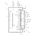
図1は、本発明の第1の実施形態である成膜装置の一実施形態を示す概略構成図である。図2(a)は、磁石対の平面図、図2(b)は金属ターゲット、誘電体枠部材及び磁石対の位置関係を示す平面図である。
(First embodiment)
FIG. 1 is a schematic configuration diagram showing an embodiment of a film forming apparatus according to the first embodiment of the present invention. 2A is a plan view of the magnet pair, and FIG. 2B is a plan view showing the positional relationship between the metal target, the dielectric frame member, and the magnet pair.
図1に示すように、本実施形態の成膜装置1は、真空雰囲気内に配置された金属ターゲット10上にプラズマを生成し、その生成されたプラズマによってターゲット原子を放出させ、その放出粒子をワークホルダ7に保持された基板W上に付着及び堆積させる反応性直流スパッタ法を用いた成膜装置である。この成膜装置1は、直流電源12及び磁石対8(磁場発生手段)等を主体としたスパッタ装置3を具備する。
As shown in FIG. 1, the
直流反応性スパッタは、直流スパッタにおいて反応性ガスを導入し、金属粒子(スパッタ粒子)を酸化させて基板W上に誘電体薄膜を形成する技術である。この技術は、直流電源12で放電を発生させてスパッタを行うため、装置構成がシンプルで成膜レートが速いというメリットがある。
DC reactive sputtering is a technique for forming a dielectric thin film on a substrate W by introducing reactive gas in DC sputtering and oxidizing metal particles (sputtered particles). This technique has an advantage that the apparatus configuration is simple and the film formation rate is fast because sputtering is performed by generating a discharge with the
本実施形態の成膜装置について詳述する。
図1に示すように、本実施形態の成膜装置1は、成膜室として真空状態の維持を可能とした真空チャンバ2と、真空チャンバ2内に収容された基板Wの表面に無機材料からなる薄膜をスパッタ法により形成するスパッタ装置3とを備えている。
真空チャンバ2は、内部を減圧雰囲気にするための真空排気系4と、真空チャンバ2内に放電用のスパッタリングガスをその流量を調整しながら供給するための第1のガス供給手段5と、真空チャンバ2内に反応性ガスをその流量を調整しながら供給するための第2のガス供給手段6と、内部に基板を保持するためのワークホルダ7とを有してなる。
The film forming apparatus of this embodiment will be described in detail.
As shown in FIG. 1, a
The
真空チャンバ2には真空排気系4が接続されているので、この真空排気系4が稼動すると真空チャンバ2の内部が排気されて真空雰囲気となる。その後、真空チャンバ2内に第1のガス供給手段5を通してスパッタリングガスとしてのアルゴンガス(Ar)が導入され、所定の真空度に設定される。スパッタ成膜を行う対象物としての基板Wはこの真空雰囲気内に配置される。
Since the vacuum exhaust system 4 is connected to the
また、スパッタ装置3は、磁石対8が配置された電極部9と、電極部9に支持され且つ金属ターゲット10を保持するバッキングプレート11と、電極部9を介して金属ターゲット10に接続された直流電源12とを有し、電圧を印加することで金属ターゲット10の表面上にプラズマ発生領域13を形成する。
本実施形態においては、バッキングプレート11上に配置される金属ターゲット10の外周を取り囲むようにして誘電体枠部材14が配置されている。
Further, the sputtering apparatus 3 was connected to the
In the present embodiment, the
電極部9は、マグネトロンカソードとして公知のもので、真空チャンバ2外に配置され直流電源12から電力が供給される。この電極部9内には金属ターゲット10の表面に磁界を与える磁石対8が配置されており、永久磁石、電磁石、或いはこれらを組み合わせた磁石等からなる。図2(a)に示すように、磁石対8は同心円状の永久磁石であって、中心磁石8Bとそれを取り囲む環状磁石8Aとで極性が異なる。
The
図1に示すように、金属ターゲット10は、電極部9に支持されたバッキングプレート11上に配置され、基板上に形成する無機膜の構成物質を含む材料、例えばシリコンからなるものとされる。金属ターゲット10(電極部9)には直流電源12が接続されており、直流電源12から電極部9を介して金属ターゲット10に電圧が印加され、金属ターゲット10の表面上にプラズマを発生させるようになっている。
As shown in FIG. 1, the
金属ターゲット10の外周を取り囲む誘電体枠部材14は、金属ターゲット10と同一材料を用いた酸化物素材(SiO2)もしくは窒化物素材(SiN)などからなり、該誘電体枠部材14と金属ターゲット10とでバッキングプレート11の表面全体を覆う形状となっている。誘電体枠部材14は、所定の厚みを有して形成され、その厚さは直流電源12により印加された電圧がチャージアップして異常放電が発生しない厚さとされ、本実施形態においては金属ターゲット10と同じ厚さとされている。金属ターゲット10と同じ厚さとすることで、金属ターゲット10の側面が誘電体枠部材14によって覆われることになる。
なお、誘電体枠部材14は、バッキングプレート11と別体であっても一体に形成されていてもよい。
The
The
誘電体枠部材14の背面側には、上記した磁石対8の環状磁石8Aが、誘電体枠部材14の内周端あるいは外周端に沿うようにして配置されている。磁石対8の環状磁石8Aを金属ターゲット10よりも面方向外側であって、誘電体枠部材14と(バッキングプレート11を介して)対向するように配置することによって、磁石対8による磁界が誘電体枠部材14上にまで及ぶことになる。このように、金属ターゲット10の全表面及び誘電体枠部材14にかかるようにプラズマ発生領域13が制御された磁場を形成することによって、少なくとも金属ターゲット10の全表面をエロージョン領域とすることができる。
On the back side of the
また、スパッタ装置3には、バッキングプレート11を介して金属ターゲット10を冷却するための冷却手段16が接続されている。バッキングプレート11には冷媒を流通させるための冷却流路(図示略)が形成されており、冷却手段16はかかる冷却流路に対して冷媒の循環を行うことによって金属ターゲット10の冷却を行うようになっている。
In addition, a cooling
真空チャンバ2内には、カソードであるターゲット10の放電領域を規制するためのシールド板17が設けられており、カソードシースより小さくなるようにカソードとのギャップを設け、カソード周辺にアースに接続され設置される。シールド板17は、電極部9及び誘電体枠部材14の外周を取り囲むようにして真空チャンバ2の底部に立設されており、誘電体枠部材14上に位置する遮蔽部17aに金属ターゲット10の平面領域よりも大きい開口17bが形成されている(図2(b)参照)。
A
[成膜方法]
上述した構成の成膜装置1を使用して反応性直流スパッタにより基板Wに無機酸化膜を形成するには、まず、真空チャンバ2内を排気してスパッタ用のアルゴンガス(Ar)を電極部9近傍の第1のガス供給手段5から適宜導入して圧力を調整した後、直流電源12により直流電圧を金属ターゲット10に印加すると、金属ターゲット10の全面及び誘電体枠部材14上にプラズマが発生する。導入されたアルゴンガスは、プラズマによって励起及びイオン化される。そして、プラズマ雰囲気中のアルゴンイオン等によって金属ターゲット10及び誘電体枠部材14がスパッタされる。また、磁石対8の磁界により、プラズマ密度の高いプラズマ発生領域13が発生し、アルゴンイオンの金属ターゲット10への衝突量が増加する。そして、その領域、すなわちエロージョンエリアからスパッタ粒子が飛散することになる。
[Film formation method]
In order to form an inorganic oxide film on the substrate W by reactive direct current sputtering using the
本実施形態におけるエロージョン領域は、金属ターゲット10の全表面及び誘電体枠部材14の表面の一部を含む範囲である。基板Wの被成膜面上に飛来したスパッタ粒子は、第2のガス供給手段6から導入された酸素(O2)と反応することで、金属酸化膜を基板W上に形成することができる。本実施形態では、シリコン(Si)を使用していることからSiO2の無機酸化膜を形成することができる。
The erosion region in the present embodiment is a range including the entire surface of the
なお、金属ターゲット10には、化合して金属酸化膜を形成する各種の金属の使用が可能である。また、金属ターゲット10の種類だけでなく、反応性ガスを適宜選択することで種々の絶縁膜を形成することができ、例えば、窒素ガスを導入することによって、基板上に金属窒化膜を形成することができる。このとき、外周に設置される誘電体材料14は、反応性ガスと同一元素を含む金属化合物としておく必要があり、窒素ガスを用いる場合は、金属窒化物を用いる。
The
本実施形態では、金属ターゲット10上及び誘電体枠部材14上にプラズマ発生領域13がかかるように磁場を発生させることができるので、少なくとも金属ターゲット10の全表面がエロージョン領域となる。そのため、金属ターゲット10の表面に酸化膜が形成されることがなく、異常放電の発生を極めて低くすることができる。誘電体枠部材14上がプラズマ発生領域13に晒されても、直流電圧下においてはプラズマプローティング電位にチャージアップはするが原理的にスパッタされるほどのバイアスが殆どかからないため、イオン拡散によるスパッタリングのみで僅かしか削れず成膜に影響は及ばない。たとえ誘電体枠部材14がスパッタされたとしても、そのスパッタ粒子は金属ターゲット10と同一の成分を含む金属酸化物であることから成膜への影響はない。
In this embodiment, since a magnetic field can be generated so that the
また、誘電体枠部材14は、数ミリ以上のバルクから形成されているので、プラズマに晒されて表面がチャージアップしても絶縁破壊による異常放電は生じない。したがって、誘電体枠部材14を設けても異常放電によるプラズマの不安定化やパーティクルの発生は起きない。また、誘電体枠部材14によって金属ターゲット10の側面やバッキングプレート11上が覆われているので、これらにスパッタ粒子が付着することが防止される。
Further, since the
また、シールド板17の下方にスパッタ粒子が廻りこんで、エロージョン領域以外の誘電体枠部材14上に反応性スパッタによる酸化膜が形成された場合でも、成膜材料と同一の材料であることから密着性が良く膜剥がれもし難い。
In addition, even when sputtered particles travel below the
以上により、金属ターゲット10の側面やバッキングプレート11上の酸化膜形成による異常放電の発生が防止されて、安定した放電を維持することができる。これにより、パーティクルの発生が低減されるので膜性能が向上する。また、装置稼働率が向上し、生産性アップに繋がる。
As described above, the occurrence of abnormal discharge due to the formation of an oxide film on the side surface of the
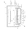
[第2実施形態の成膜装置]
図3は、本発明の第2実施形態に係る成膜装置の構成を示す模式図である。
以下の説明では、先の実施形態の同様の構造及び同一部材には同一符号を付して、その詳細な説明は省略または簡略化する。
本実施形態は、2枚の金属ターゲットを対向配置してなる対向ターゲット方式の成膜装置である。
[Film Forming Apparatus of Second Embodiment]
FIG. 3 is a schematic diagram showing a configuration of a film forming apparatus according to the second embodiment of the present invention.
In the following description, the same reference numerals are given to the same structures and the same members in the previous embodiment, and the detailed description thereof is omitted or simplified.
The present embodiment is a facing target type film forming apparatus in which two metal targets are disposed to face each other.
図3に示すように、本実施形態の成膜装置18は、基板Wを収容する真空チャンバ2と、真空チャンバ2内の基板Wの被成膜面に金属酸化膜を形成するスパッタ装置40とが装置接続部22を介して接続された構成を備えている。
As shown in FIG. 3, the
スパッタ装置40は、金属ターゲット10a、磁石対8、電極部9、バッキングプレート11、直流電源12、冷却手段16を有するプラズマ発生手段20Aと、金属ターゲット10b、磁石対8、電極部9、バッキングプレート11、直流電源12、冷却手段16を有するプラズマ発生手段20Bとを備えており、真空チャンバ2内に配置された基板Wの被成膜面(表面)に対して2枚の金属ターゲット10a,10bが垂直姿勢に保持されている。
The
各金属ターゲット10a,10bは、各々の外周が誘電体枠部材14a、14bによって取り囲まれており、金属ターゲット10a,10b同士の対向面及び誘電体枠部材14a,14b同士の対向面が略平行となるように設置されている。
The outer peripheries of the
各金属ターゲット10a、10b(各電極部9,9)にはそれぞれ直流電源12が接続され、各直流電源12から供給される電力によって金属ターゲット10a,10b及び誘電体枠部材14a,14b同士が対向する空間にそれぞれプラズマを発生させるようになっている。
A direct
スパッタ装置40は、そのプラズマ発生領域13に放電用のアルゴンガス(Ar)を流通させる第1のガス供給手段5を備えており、金属ターゲット10a,10bに挟まれるプラズマ発生領域13に対して真空チャンバ2と反対側に配置された側壁部材21に接続されている。第1のガス供給手段5から供給されるアルゴンガス(Ar)は、側壁部材21側からプラズマ発生領域13に流入し、装置接続部22を介して真空チャンバ2の上方に向けて流入するようになっている。一方、真空チャンバ2には、その内部に反応性ガスとして酸素(O2)を供給するための第2のガス供給手段6が備えられており、基板Wの近傍に酸素(O2)が流入するようになっている。
The
また、各シールド板17は、第1の実施形態と同じように、各誘電体枠部材14a,14bの外周を取り囲むようにして配置されており、遮蔽部17aの端部が誘電体枠部材14a,14b上に位置している。すなわち、シールド板17の開口17bが、金属ターゲット10a,10bの平面領域よりも大きくなっている
Each
なお、本実施形態においても、各電極部9に接続された冷却手段16によって、各電極部9内に形成される冷却流路Rに対して冷媒の循環を行う構成となっており、バッキングプレート11,11を介して各金属ターゲット10a,10bを所望の温度に冷却する。
In the present embodiment, the cooling means 16 connected to each
[成膜方法]
本実施形態の成膜装置18により基板W上に金属酸化膜を形成するには、図3に示すように、第1のガス供給手段5からアルゴン(Ar)ガスを導入しながら、金属ターゲット10a及び金属ターゲット10bに直流電力を供給することで、これら2枚の金属ターゲット10a,10bに挟まれる空間にプラズマを発生させる。具体的には、各金属ターゲット10a,10bの全表面と各誘電体枠部材14a,14bの表面の一部にプラズマ発生領域13がかかるようにそれぞれ磁場を発生させ、プラズマ雰囲気中のアルゴンイオン等を各金属ターゲット10a,10bに衝突させることで、各金属ターゲット10a,10bから成膜材料(シリコン)をスパッタ粒子としてたたき出す。
[Film formation method]
In order to form a metal oxide film on the substrate W by the
第1のガス供給手段5からアルゴンガスを導入してプラズマを発生した後、真空チャンバ2内に第2のガス供給手段6から酸素ガスを導入する。そして、スパッタ装置40側から飛来したスパッタ粒子と、基板Wの近傍に設けられた第2のガス供給手段6から供給された酸素ガスとを基板Wの被成膜面上で反応させることで、金属酸化物からなる薄膜を基板W上にそれぞれ形成するようになっている。
After introducing argon gas from the first gas supply means 5 to generate plasma, oxygen gas is introduced from the second gas supply means 6 into the
このように、本実施形態においても、上記第1の実施形態同様の作用効果を得ることができる。本実施形態では、2枚の金属ターゲット10a,10bを用いることによってライン状成膜が可能となり、基板を搬送して成膜することにより大型基板への適応も可能となる。また、金属ターゲット10a,10b同士の間隔を狭くすることにより、スパッタ装置40から装置接続部22を解して対向するターゲット方位に関して放出されるスパッタ粒子の指向性を高めることができるので、形成される金属酸化膜の成膜品質を向上させることができる。
As described above, also in this embodiment, the same operational effects as those in the first embodiment can be obtained. In the present embodiment, line-shaped film formation is possible by using the two
[第3実施形態の成膜装置]
図4は、本発明の第3実施形態に係る成膜装置の構成を示す模式図である。
以下の説明では、先の実施形態の同様の構造及び同一部材には同一符号を付して、その詳細な説明は省略または簡略化する。
本実施形態は、第2実施形態同様に、2枚の金属ターゲットを対向配置してなる対向ターゲット方式の成膜装置であるが、磁場発生手段の構成において異なる。
[Film Forming Apparatus of Third Embodiment]
FIG. 4 is a schematic diagram showing a configuration of a film forming apparatus according to the third embodiment of the present invention.
In the following description, the same reference numerals are given to the same structures and the same members in the previous embodiment, and the detailed description thereof is omitted or simplified.
As in the second embodiment, the present embodiment is a facing target type film forming apparatus in which two metal targets are arranged to face each other, but differs in the configuration of the magnetic field generating means.
図4に示すように、本実施形態のスパッタ装置50における各プラズマ発生手段25A,25Bには、金属ターゲット10a,10bの外周端に沿うような環状の磁石からなる磁場発生手段26a,26bが設けられている。第1の磁場発生手段26aは誘電体枠部材14aの背面側に配置され、第2の磁場発生手段26bは誘電体枠部材14bの背面側に配置されている。したがって、第1の磁場発生手段26aと第2の磁場発生手段26bとは、対向配置された金属ターゲット10a,10bの周縁部外側において互いに対向配置されている。
なお、これら第1の磁場発生手段26aと第2の磁場発生手段26bとの極性は異なっている。
As shown in FIG. 4, the plasma generating means 25A and 25B in the
The first magnetic field generating means 26a and the second magnetic field generating means 26b have different polarities.
成膜動作に際して、これら対向する磁場発生手段26a,26bによって金属ターゲット10a,10bを取り囲む磁場が形成される。そのため、本実施形態の成膜装置27では、かかる磁界によってプラズマに含まれる電子を捕捉ないし反射させることができるので、対向する金属ターゲット10a,10bの間の空間内にプラズマを良好に閉じ込めることができる。
During the film forming operation, a magnetic field surrounding the
[第4実施形態の成膜装置]
図5は、本発明の第4実施形態に係る成膜装置の構成を示す模式図である。
以下の説明では、先の実施形態の同様の構造及び同一部材には同一符号を付して、その詳細な説明は省略または簡略化する。
図5に示すように、本実施形態はマグネットスキャン式の成膜装置30であって、同心円状にN極、S極を配置した円状の磁場発生手段32をスパッタ装置60に備える。
[Film Forming Apparatus of Fourth Embodiment]
FIG. 5 is a schematic view showing a configuration of a film forming apparatus according to the fourth embodiment of the present invention.
In the following description, the same reference numerals are given to the same structures and the same members in the previous embodiment, and the detailed description thereof is omitted or simplified.
As shown in FIG. 5, the present embodiment is a magnet scan type
磁場発生手段32は電極部9(金属ターゲット10)の中心より偏って配置され、少なくとも環状の磁石31が金属ターゲット10の周縁部よりも外側、すなわち誘電体枠部材14の背面側となるように配置されている。このような磁場発生手段32は、複数の磁石31を金属ターゲット10の面方向(図中の矢印で示す方向)に沿って偏心運動できるように構成されている。
The magnetic field generating means 32 is arranged to be deviated from the center of the electrode portion 9 (metal target 10) so that at least the
成膜動作を行う際には磁場発生手段32を偏心運動させることになるが、このとき、磁場発生手段32を構成する環状の磁石31の一部が、常に誘電体枠部材14と平面的に重なるように偏心運動をさせる。このように、複数の磁石31を、金属ターゲット10に対して相対的に偏心移動させることでその磁場も移動し、少なくとも金属ターゲット10の全表面及び誘電体枠部材14の一部をエロージョン領域とすることができる。
When the film forming operation is performed, the magnetic
なお、磁石31の形状は、上記した形状に限ったものではなく、同心円状のマグネット構造ではなく、四角状などの複数の磁石の組み合わせによって長円状としてもよい。
In addition, the shape of the
以上述べたように、本発明によれば、金属ターゲット10の全表面及び誘電体枠部材14上にプラズマ発生領域13がかかるように磁場を形成することによって、少なくとも金属ターゲット10の全表面をエロージョンエリアとすることができる。そのため、金属ターゲット10の表面にスパッタ粒子(酸化物)が堆積することが防止される。また、金属ターゲット10の外周を取り囲む誘電体枠部材14によって、金属ターゲット10の側面やバッキングプレート11上にスパッタ粒子(酸化物)が堆積することが防止される。このように、所定の厚さを有した誘電体枠部材14を設けることにより、エロージョンエリア以外の部分に堆積する酸化物のチャージアップを防止することができる。また、金属ターゲット10やバッキングプレート11に対する酸化物の堆積を抑制して異常放電を防止し、プラズマを安定させることとなる。
As described above, according to the present invention, at least the entire surface of the
したがって、膜質均一性が向上し、パーティクルを減少させることができる。また、金属ターゲット10の表面全体がエロージョン領域となることから成膜速度が向上する。
さらに、スパッタ率の低い酸化物の堆積が抑制されるため成膜速度の低下を防止できるなどの効果を発揮する。
Therefore, film quality uniformity can be improved and particles can be reduced. Further, since the entire surface of the
Further, since the deposition of an oxide having a low sputtering rate is suppressed, the effect of preventing the film formation rate from decreasing can be exhibited.
以上、添付図面を参照しながら本発明に係る好適な実施形態について説明したが、本発明は係る例に限定されないことは言うまでもなく、上記各実施形態を組み合わせても良い。当業者であれば、特許請求の範囲に記載された技術的思想の範疇内において、各種の変更例または修正例に想到し得ることは明らかであり、それらについても当然に本発明の技術的範囲に属するものと了解される。 The preferred embodiments according to the present invention have been described above with reference to the accompanying drawings. However, it goes without saying that the present invention is not limited to such examples, and the above embodiments may be combined. It is obvious for those skilled in the art that various changes or modifications can be conceived within the scope of the technical idea described in the claims. It is understood that it belongs to.
上記実施形態においては、ターゲット形状を円状とし、磁石対の形状を同心円状としたが、磁石対のうち一方の磁石を細棒状とし、これを取り囲む他方の磁石を矩形枠状としても良い。また、ターゲットは四角であって、磁石形状もそれに準じた構造としても構わない。
また、直流電源12の他に高周波電源を設けるようにしても良い。直流電圧に加えて高周波電圧を同時に印加することにより、酸化物のチャージアップを防止してプラズマを安定化することができる。
また、金属ターゲット10と電極部9との間に直流電圧をパルス状に印加しても良い。これにより、エロージョンエリア以外の領域に酸化膜が形成されたとしても、その酸化膜のチャージアップを防止することができる。
In the above embodiment, the target shape is circular, and the shape of the magnet pair is concentric. However, one magnet of the magnet pair may be a thin rod, and the other magnet surrounding the magnet may be a rectangular frame. Further, the target may be a square, and the magnet shape may be a structure conforming thereto.
In addition to the
Further, a DC voltage may be applied in a pulsed manner between the
1,18,27,30…成膜装置、12…直流電源、14,14a,14b…誘電体枠部材、9…電極部、13…プラズマ発生領域、10,10a,10b…金属ターゲット、8…磁石対(磁場発生手段)、8A…中心磁石、8B…環状磁石、16…冷却手段、17…シールド板、17b…開口、26a,26b…磁場発生手段、31…磁石、32…磁場発生手段
DESCRIPTION OF
Claims (9)
直流電源と、
前記直流電源に接続される金属ターゲットと、
前記金属ターゲットの外周を取り囲むようにして配置される誘電体枠部材と、
前記金属ターゲットの背面側に配置される電極部と、
前記金属ターゲット及び前記誘電体枠部材の背面側に配置される磁場発生手段と、を有し、
前記磁場発生手段の少なくとも一部が前記誘電体枠部材に沿うように配置されていることを特徴とする成膜装置。 In reactive DC type film forming equipment,
DC power supply,
A metal target connected to the DC power source;
A dielectric frame member disposed so as to surround the outer periphery of the metal target;
An electrode part disposed on the back side of the metal target;
Magnetic field generating means disposed on the back side of the metal target and the dielectric frame member,
The film forming apparatus, wherein at least a part of the magnetic field generating means is disposed along the dielectric frame member.
前記プラズマ発生領域が前記金属ターゲットの平面領域よりも大きいことを特徴とする請求項1乃至3のいずれか一項に記載の成膜装置。 A shield plate is disposed outside the plasma generation region on the dielectric frame member,
The film forming apparatus according to claim 1, wherein the plasma generation region is larger than a planar region of the metal target.
前記プラズマ発生領域を挟んで配置された前記複数の金属ターゲットの対向方向に磁界を発生させることを特徴とする請求項5記載の成膜装置。 The magnetic field generating means are respectively disposed on the back side of the plurality of metal targets;
The film forming apparatus according to claim 5, wherein a magnetic field is generated in a facing direction of the plurality of metal targets arranged with the plasma generation region interposed therebetween.
前記金属ターゲット上及び該金属ターゲットの外周を取り囲むようにして配置される前記誘電体枠部材上に、プラズマ発生領域がかかるように磁場を発生させることを特徴とする成膜方法。 A film forming method using the film forming apparatus according to any one of claims 1 to 7,
A film forming method, wherein a magnetic field is generated so that a plasma generating region is applied on the metal target and on the dielectric frame member disposed so as to surround an outer periphery of the metal target.
Priority Applications (2)
| Application Number | Priority Date | Filing Date | Title |
|---|---|---|---|
| JP2008035643A JP2009191340A (en) | 2008-02-18 | 2008-02-18 | Film-forming apparatus and film-forming method |
| US12/364,545 US20090205950A1 (en) | 2008-02-18 | 2009-02-03 | Film deposition apparatus and film deposition method |
Applications Claiming Priority (1)
| Application Number | Priority Date | Filing Date | Title |
|---|---|---|---|
| JP2008035643A JP2009191340A (en) | 2008-02-18 | 2008-02-18 | Film-forming apparatus and film-forming method |
Publications (2)
| Publication Number | Publication Date |
|---|---|
| JP2009191340A true JP2009191340A (en) | 2009-08-27 |
| JP2009191340A5 JP2009191340A5 (en) | 2011-03-17 |
Family
ID=40954106
Family Applications (1)
| Application Number | Title | Priority Date | Filing Date |
|---|---|---|---|
| JP2008035643A Withdrawn JP2009191340A (en) | 2008-02-18 | 2008-02-18 | Film-forming apparatus and film-forming method |
Country Status (2)
| Country | Link |
|---|---|
| US (1) | US20090205950A1 (en) |
| JP (1) | JP2009191340A (en) |
Cited By (2)
| Publication number | Priority date | Publication date | Assignee | Title |
|---|---|---|---|---|
| WO2011148488A1 (en) * | 2010-05-27 | 2011-12-01 | 株式会社ナチュラテクノロジー | Naturatron sputtering device |
| JP7150364B1 (en) * | 2021-09-27 | 2022-10-11 | 株式会社アドバンスト・スパッタテック | Sputtering deposition source and deposition equipment |
Families Citing this family (3)
| Publication number | Priority date | Publication date | Assignee | Title |
|---|---|---|---|---|
| KR20130023282A (en) * | 2010-06-03 | 2013-03-07 | 울박, 인크 | Sputter deposition device |
| KR20130035256A (en) * | 2010-06-03 | 2013-04-08 | 울박, 인크 | Sputter deposition device |
| CN103469165B (en) * | 2013-10-10 | 2016-06-08 | 黄志宏 | Based on the rectangle plane cathode arc target of distributed electrical magnet |
Citations (7)
| Publication number | Priority date | Publication date | Assignee | Title |
|---|---|---|---|---|
| JPS63466A (en) * | 1986-06-18 | 1988-01-05 | Matsushita Electric Ind Co Ltd | Sputtering target |
| JPH02236277A (en) * | 1989-03-09 | 1990-09-19 | Fujitsu Ltd | Sputtering method |
| JPH02305960A (en) * | 1989-05-18 | 1990-12-19 | Sony Corp | Reactive magnetron sputtering device |
| JPH0375366A (en) * | 1989-08-17 | 1991-03-29 | Mitsubishi Kasei Corp | Sputtering target |
| JPH0397846A (en) * | 1989-09-07 | 1991-04-23 | Kao Corp | Formation of thin film of silicon compound |
| JPH03100173A (en) * | 1989-09-14 | 1991-04-25 | Mitsubishi Kasei Corp | Dc magnetron type reactive sputtering device |
| JPH07243039A (en) * | 1994-03-02 | 1995-09-19 | Chugai Ro Co Ltd | Dc-magnetron reactive sputtering method |
Family Cites Families (3)
| Publication number | Priority date | Publication date | Assignee | Title |
|---|---|---|---|---|
| US4622122A (en) * | 1986-02-24 | 1986-11-11 | Oerlikon Buhrle U.S.A. Inc. | Planar magnetron cathode target assembly |
| US5922176A (en) * | 1992-06-12 | 1999-07-13 | Donnelly Corporation | Spark eliminating sputtering target and method for using and making same |
| US5637199A (en) * | 1992-06-26 | 1997-06-10 | Minnesota Mining And Manufacturing Company | Sputtering shields and method of manufacture |
-
2008
- 2008-02-18 JP JP2008035643A patent/JP2009191340A/en not_active Withdrawn
-
2009
- 2009-02-03 US US12/364,545 patent/US20090205950A1/en not_active Abandoned
Patent Citations (7)
| Publication number | Priority date | Publication date | Assignee | Title |
|---|---|---|---|---|
| JPS63466A (en) * | 1986-06-18 | 1988-01-05 | Matsushita Electric Ind Co Ltd | Sputtering target |
| JPH02236277A (en) * | 1989-03-09 | 1990-09-19 | Fujitsu Ltd | Sputtering method |
| JPH02305960A (en) * | 1989-05-18 | 1990-12-19 | Sony Corp | Reactive magnetron sputtering device |
| JPH0375366A (en) * | 1989-08-17 | 1991-03-29 | Mitsubishi Kasei Corp | Sputtering target |
| JPH0397846A (en) * | 1989-09-07 | 1991-04-23 | Kao Corp | Formation of thin film of silicon compound |
| JPH03100173A (en) * | 1989-09-14 | 1991-04-25 | Mitsubishi Kasei Corp | Dc magnetron type reactive sputtering device |
| JPH07243039A (en) * | 1994-03-02 | 1995-09-19 | Chugai Ro Co Ltd | Dc-magnetron reactive sputtering method |
Cited By (3)
| Publication number | Priority date | Publication date | Assignee | Title |
|---|---|---|---|---|
| WO2011148488A1 (en) * | 2010-05-27 | 2011-12-01 | 株式会社ナチュラテクノロジー | Naturatron sputtering device |
| JP7150364B1 (en) * | 2021-09-27 | 2022-10-11 | 株式会社アドバンスト・スパッタテック | Sputtering deposition source and deposition equipment |
| WO2023047995A1 (en) * | 2021-09-27 | 2023-03-30 | 株式会社アドバンスト・スパッタテック | Sputtering deposition source and deposition device |
Also Published As
| Publication number | Publication date |
|---|---|
| US20090205950A1 (en) | 2009-08-20 |
Similar Documents
| Publication | Publication Date | Title |
|---|---|---|
| TWI414621B (en) | Sputtering target and sputtering method using the target | |
| JP5527894B2 (en) | Sputtering equipment | |
| JP5282167B2 (en) | Sputter deposition system | |
| JP2009191340A (en) | Film-forming apparatus and film-forming method | |
| JP2002173767A (en) | Facing target sputtering method and method for depositing electro-conductive film | |
| KR20210089740A (en) | Inclined magnetron in PVD sputtering deposition chamber | |
| JP2010248576A (en) | Magnetron sputtering apparatus | |
| US9368331B2 (en) | Sputtering apparatus | |
| JP3080945B1 (en) | High efficiency plasma gas condensing cluster deposition system | |
| JP4614936B2 (en) | Composite type sputtering apparatus and composite type sputtering method | |
| JP5853487B2 (en) | Discharge electrode and discharge method | |
| JP2010255052A (en) | Sputtering method | |
| JP2013001943A (en) | Sputtering apparatus | |
| WO2020004619A1 (en) | Sputter deposition device | |
| JPH07233473A (en) | Magnetron sputtering device | |
| JP2001081550A (en) | Reactive sputtering system, and method of film deposition | |
| JP2013129871A (en) | Magnetron sputtering cathode and sputtering apparatus equipped with the same | |
| WO2016208094A1 (en) | Vacuum arc film-forming apparatus and film-forming method | |
| JP2007291477A (en) | Sputtering apparatus | |
| JP2020180339A (en) | Sputtering apparatus and sputtering method | |
| US20060081467A1 (en) | Systems and methods for magnetron deposition | |
| JPH01111870A (en) | Sputtering device | |
| JP2013079420A (en) | Sputtering apparatus | |
| JP2006022372A (en) | Magnetron cathode electrode, and sputtering method using the same | |
| CN211897094U (en) | Hardware configuration and system for physical sputtering |
Legal Events
| Date | Code | Title | Description |
|---|---|---|---|
| A521 | Written amendment |
Free format text: JAPANESE INTERMEDIATE CODE: A523 Effective date: 20110131 |
|
| A621 | Written request for application examination |
Free format text: JAPANESE INTERMEDIATE CODE: A621 Effective date: 20110131 |
|
| A977 | Report on retrieval |
Free format text: JAPANESE INTERMEDIATE CODE: A971007 Effective date: 20120528 |
|
| A131 | Notification of reasons for refusal |
Free format text: JAPANESE INTERMEDIATE CODE: A131 Effective date: 20120605 |
|
| A761 | Written withdrawal of application |
Free format text: JAPANESE INTERMEDIATE CODE: A761 Effective date: 20120702 |