JP2009188378A - Pulse train annealing method and device - Google Patents
Pulse train annealing method and device Download PDFInfo
- Publication number
- JP2009188378A JP2009188378A JP2008287019A JP2008287019A JP2009188378A JP 2009188378 A JP2009188378 A JP 2009188378A JP 2008287019 A JP2008287019 A JP 2008287019A JP 2008287019 A JP2008287019 A JP 2008287019A JP 2009188378 A JP2009188378 A JP 2009188378A
- Authority
- JP
- Japan
- Prior art keywords
- substrate
- energy
- pulse
- pulses
- region
- Prior art date
- Legal status (The legal status is an assumption and is not a legal conclusion. Google has not performed a legal analysis and makes no representation as to the accuracy of the status listed.)
- Pending
Links
- 238000000034 method Methods 0.000 title claims abstract description 172
- 238000000137 annealing Methods 0.000 title claims abstract description 124
- 239000000758 substrate Substances 0.000 claims abstract description 450
- 230000005855 radiation Effects 0.000 claims abstract description 81
- 238000012545 processing Methods 0.000 claims description 33
- 230000005670 electromagnetic radiation Effects 0.000 claims description 27
- 230000003287 optical effect Effects 0.000 claims description 21
- 230000001939 inductive effect Effects 0.000 claims description 4
- 230000008569 process Effects 0.000 abstract description 129
- 239000000463 material Substances 0.000 abstract description 57
- 238000002844 melting Methods 0.000 abstract description 32
- 230000008018 melting Effects 0.000 abstract description 31
- 230000000694 effects Effects 0.000 abstract description 11
- 239000002019 doping agent Substances 0.000 description 75
- 239000013078 crystal Substances 0.000 description 52
- XUIMIQQOPSSXEZ-UHFFFAOYSA-N Silicon Chemical compound [Si] XUIMIQQOPSSXEZ-UHFFFAOYSA-N 0.000 description 35
- 229910052710 silicon Inorganic materials 0.000 description 33
- 239000010703 silicon Substances 0.000 description 32
- 239000010410 layer Substances 0.000 description 31
- 238000010438 heat treatment Methods 0.000 description 28
- 239000004065 semiconductor Substances 0.000 description 26
- 238000000576 coating method Methods 0.000 description 25
- 239000011248 coating agent Substances 0.000 description 23
- 230000008859 change Effects 0.000 description 21
- 238000009792 diffusion process Methods 0.000 description 20
- 230000033001 locomotion Effects 0.000 description 17
- 230000004044 response Effects 0.000 description 16
- 230000007547 defect Effects 0.000 description 15
- 239000003990 capacitor Substances 0.000 description 13
- 238000001816 cooling Methods 0.000 description 11
- 230000006870 function Effects 0.000 description 11
- 239000007789 gas Substances 0.000 description 11
- 238000010586 diagram Methods 0.000 description 9
- 238000009826 distribution Methods 0.000 description 9
- 238000002310 reflectometry Methods 0.000 description 9
- XKRFYHLGVUSROY-UHFFFAOYSA-N Argon Chemical compound [Ar] XKRFYHLGVUSROY-UHFFFAOYSA-N 0.000 description 8
- 239000000956 alloy Substances 0.000 description 8
- 230000004048 modification Effects 0.000 description 8
- 238000012986 modification Methods 0.000 description 8
- OKTJSMMVPCPJKN-UHFFFAOYSA-N Carbon Chemical compound [C] OKTJSMMVPCPJKN-UHFFFAOYSA-N 0.000 description 7
- 229910052799 carbon Inorganic materials 0.000 description 7
- 229910052732 germanium Inorganic materials 0.000 description 7
- GNPVGFCGXDBREM-UHFFFAOYSA-N germanium atom Chemical compound [Ge] GNPVGFCGXDBREM-UHFFFAOYSA-N 0.000 description 7
- 150000001875 compounds Chemical class 0.000 description 6
- 238000004519 manufacturing process Methods 0.000 description 6
- 230000015654 memory Effects 0.000 description 6
- PXHVJJICTQNCMI-UHFFFAOYSA-N nickel Substances [Ni] PXHVJJICTQNCMI-UHFFFAOYSA-N 0.000 description 6
- IJGRMHOSHXDMSA-UHFFFAOYSA-N Atomic nitrogen Chemical compound N#N IJGRMHOSHXDMSA-UHFFFAOYSA-N 0.000 description 5
- 230000004913 activation Effects 0.000 description 5
- 239000013590 bulk material Substances 0.000 description 5
- 230000007423 decrease Effects 0.000 description 5
- 230000001976 improved effect Effects 0.000 description 5
- 230000001965 increasing effect Effects 0.000 description 5
- 238000005224 laser annealing Methods 0.000 description 5
- 229910052751 metal Inorganic materials 0.000 description 5
- 239000002184 metal Substances 0.000 description 5
- 238000012544 monitoring process Methods 0.000 description 5
- VYPSYNLAJGMNEJ-UHFFFAOYSA-N silicon dioxide Inorganic materials O=[Si]=O VYPSYNLAJGMNEJ-UHFFFAOYSA-N 0.000 description 5
- 238000012546 transfer Methods 0.000 description 5
- ZOXJGFHDIHLPTG-UHFFFAOYSA-N Boron Chemical compound [B] ZOXJGFHDIHLPTG-UHFFFAOYSA-N 0.000 description 4
- 238000010521 absorption reaction Methods 0.000 description 4
- 229910045601 alloy Inorganic materials 0.000 description 4
- 229910052786 argon Inorganic materials 0.000 description 4
- 229910052785 arsenic Inorganic materials 0.000 description 4
- RQNWIZPPADIBDY-UHFFFAOYSA-N arsenic atom Chemical compound [As] RQNWIZPPADIBDY-UHFFFAOYSA-N 0.000 description 4
- 238000000151 deposition Methods 0.000 description 4
- 239000012530 fluid Substances 0.000 description 4
- 238000002513 implantation Methods 0.000 description 4
- 238000010884 ion-beam technique Methods 0.000 description 4
- 238000004151 rapid thermal annealing Methods 0.000 description 4
- 229910052721 tungsten Inorganic materials 0.000 description 4
- -1 tungsten halogen Chemical class 0.000 description 4
- JBRZTFJDHDCESZ-UHFFFAOYSA-N AsGa Chemical compound [As]#[Ga] JBRZTFJDHDCESZ-UHFFFAOYSA-N 0.000 description 3
- OAICVXFJPJFONN-UHFFFAOYSA-N Phosphorus Chemical compound [P] OAICVXFJPJFONN-UHFFFAOYSA-N 0.000 description 3
- BQCADISMDOOEFD-UHFFFAOYSA-N Silver Chemical compound [Ag] BQCADISMDOOEFD-UHFFFAOYSA-N 0.000 description 3
- 238000004458 analytical method Methods 0.000 description 3
- 229910052787 antimony Inorganic materials 0.000 description 3
- WATWJIUSRGPENY-UHFFFAOYSA-N antimony atom Chemical compound [Sb] WATWJIUSRGPENY-UHFFFAOYSA-N 0.000 description 3
- 229910052796 boron Inorganic materials 0.000 description 3
- 238000005229 chemical vapour deposition Methods 0.000 description 3
- 229910017052 cobalt Inorganic materials 0.000 description 3
- 239000010941 cobalt Substances 0.000 description 3
- GUTLYIVDDKVIGB-UHFFFAOYSA-N cobalt atom Chemical compound [Co] GUTLYIVDDKVIGB-UHFFFAOYSA-N 0.000 description 3
- 238000007796 conventional method Methods 0.000 description 3
- 239000012809 cooling fluid Substances 0.000 description 3
- 238000005137 deposition process Methods 0.000 description 3
- 239000006185 dispersion Substances 0.000 description 3
- 238000010894 electron beam technology Methods 0.000 description 3
- 229910052736 halogen Inorganic materials 0.000 description 3
- 229910052698 phosphorus Inorganic materials 0.000 description 3
- 239000011574 phosphorus Substances 0.000 description 3
- 230000010287 polarization Effects 0.000 description 3
- 238000002407 reforming Methods 0.000 description 3
- 230000008439 repair process Effects 0.000 description 3
- 235000012239 silicon dioxide Nutrition 0.000 description 3
- 229910052709 silver Inorganic materials 0.000 description 3
- 239000004332 silver Substances 0.000 description 3
- 239000010936 titanium Substances 0.000 description 3
- 239000010937 tungsten Substances 0.000 description 3
- 229910001218 Gallium arsenide Inorganic materials 0.000 description 2
- JMASRVWKEDWRBT-UHFFFAOYSA-N Gallium nitride Chemical compound [Ga]#N JMASRVWKEDWRBT-UHFFFAOYSA-N 0.000 description 2
- RTAQQCXQSZGOHL-UHFFFAOYSA-N Titanium Chemical compound [Ti] RTAQQCXQSZGOHL-UHFFFAOYSA-N 0.000 description 2
- NRTOMJZYCJJWKI-UHFFFAOYSA-N Titanium nitride Chemical compound [Ti]#N NRTOMJZYCJJWKI-UHFFFAOYSA-N 0.000 description 2
- 239000002250 absorbent Substances 0.000 description 2
- 230000002745 absorbent Effects 0.000 description 2
- 230000003213 activating effect Effects 0.000 description 2
- 238000000231 atomic layer deposition Methods 0.000 description 2
- 239000000969 carrier Substances 0.000 description 2
- 238000006243 chemical reaction Methods 0.000 description 2
- 239000004020 conductor Substances 0.000 description 2
- 239000002826 coolant Substances 0.000 description 2
- 239000000112 cooling gas Substances 0.000 description 2
- 230000003247 decreasing effect Effects 0.000 description 2
- 239000003989 dielectric material Substances 0.000 description 2
- 230000005611 electricity Effects 0.000 description 2
- 230000008020 evaporation Effects 0.000 description 2
- 238000001704 evaporation Methods 0.000 description 2
- 238000010304 firing Methods 0.000 description 2
- 230000004907 flux Effects 0.000 description 2
- 239000011521 glass Substances 0.000 description 2
- 229910052738 indium Inorganic materials 0.000 description 2
- APFVFJFRJDLVQX-UHFFFAOYSA-N indium atom Chemical compound [In] APFVFJFRJDLVQX-UHFFFAOYSA-N 0.000 description 2
- 150000002500 ions Chemical class 0.000 description 2
- 230000001788 irregular Effects 0.000 description 2
- 229910052743 krypton Inorganic materials 0.000 description 2
- DNNSSWSSYDEUBZ-UHFFFAOYSA-N krypton atom Chemical compound [Kr] DNNSSWSSYDEUBZ-UHFFFAOYSA-N 0.000 description 2
- 229910052759 nickel Inorganic materials 0.000 description 2
- 229910052757 nitrogen Inorganic materials 0.000 description 2
- 239000002245 particle Substances 0.000 description 2
- 229920000642 polymer Polymers 0.000 description 2
- 239000002243 precursor Substances 0.000 description 2
- 230000008707 rearrangement Effects 0.000 description 2
- 230000035939 shock Effects 0.000 description 2
- 229910021332 silicide Inorganic materials 0.000 description 2
- HBMJWWWQQXIZIP-UHFFFAOYSA-N silicon carbide Chemical compound [Si+]#[C-] HBMJWWWQQXIZIP-UHFFFAOYSA-N 0.000 description 2
- 229910010271 silicon carbide Inorganic materials 0.000 description 2
- 239000000377 silicon dioxide Substances 0.000 description 2
- 238000001228 spectrum Methods 0.000 description 2
- 239000000126 substance Substances 0.000 description 2
- 238000004381 surface treatment Methods 0.000 description 2
- 238000010301 surface-oxidation reaction Methods 0.000 description 2
- 229910052715 tantalum Inorganic materials 0.000 description 2
- GUVRBAGPIYLISA-UHFFFAOYSA-N tantalum atom Chemical compound [Ta] GUVRBAGPIYLISA-UHFFFAOYSA-N 0.000 description 2
- 229910052719 titanium Inorganic materials 0.000 description 2
- 229910052724 xenon Inorganic materials 0.000 description 2
- FHNFHKCVQCLJFQ-UHFFFAOYSA-N xenon atom Chemical compound [Xe] FHNFHKCVQCLJFQ-UHFFFAOYSA-N 0.000 description 2
- 229910052684 Cerium Inorganic materials 0.000 description 1
- 206010010144 Completed suicide Diseases 0.000 description 1
- 206010073306 Exposure to radiation Diseases 0.000 description 1
- PXGOKWXKJXAPGV-UHFFFAOYSA-N Fluorine Chemical compound FF PXGOKWXKJXAPGV-UHFFFAOYSA-N 0.000 description 1
- GYHNNYVSQQEPJS-UHFFFAOYSA-N Gallium Chemical compound [Ga] GYHNNYVSQQEPJS-UHFFFAOYSA-N 0.000 description 1
- 229910000927 Ge alloy Inorganic materials 0.000 description 1
- 238000004616 Pyrometry Methods 0.000 description 1
- KJTLSVCANCCWHF-UHFFFAOYSA-N Ruthenium Chemical compound [Ru] KJTLSVCANCCWHF-UHFFFAOYSA-N 0.000 description 1
- ATJFFYVFTNAWJD-UHFFFAOYSA-N Tin Chemical compound [Sn] ATJFFYVFTNAWJD-UHFFFAOYSA-N 0.000 description 1
- 230000000996 additive effect Effects 0.000 description 1
- 238000005275 alloying Methods 0.000 description 1
- 229910052782 aluminium Inorganic materials 0.000 description 1
- XAGFODPZIPBFFR-UHFFFAOYSA-N aluminium Chemical compound [Al] XAGFODPZIPBFFR-UHFFFAOYSA-N 0.000 description 1
- 229910003481 amorphous carbon Inorganic materials 0.000 description 1
- 239000002194 amorphous carbon material Substances 0.000 description 1
- 230000008901 benefit Effects 0.000 description 1
- 230000015572 biosynthetic process Effects 0.000 description 1
- KYKAJFCTULSVSH-UHFFFAOYSA-N chloro(fluoro)methane Chemical compound F[C]Cl KYKAJFCTULSVSH-UHFFFAOYSA-N 0.000 description 1
- 238000004891 communication Methods 0.000 description 1
- 238000012937 correction Methods 0.000 description 1
- 230000008878 coupling Effects 0.000 description 1
- 238000010168 coupling process Methods 0.000 description 1
- 238000005859 coupling reaction Methods 0.000 description 1
- 229910021419 crystalline silicon Inorganic materials 0.000 description 1
- 230000003111 delayed effect Effects 0.000 description 1
- 230000008021 deposition Effects 0.000 description 1
- 238000013461 design Methods 0.000 description 1
- 230000001066 destructive effect Effects 0.000 description 1
- 238000001514 detection method Methods 0.000 description 1
- 238000011161 development Methods 0.000 description 1
- 238000007599 discharging Methods 0.000 description 1
- 238000006073 displacement reaction Methods 0.000 description 1
- 229910052731 fluorine Inorganic materials 0.000 description 1
- 239000011737 fluorine Substances 0.000 description 1
- 229940104869 fluorosilicate Drugs 0.000 description 1
- 229910052733 gallium Inorganic materials 0.000 description 1
- HZXMRANICFIONG-UHFFFAOYSA-N gallium phosphide Chemical compound [Ga]#P HZXMRANICFIONG-UHFFFAOYSA-N 0.000 description 1
- 238000009499 grossing Methods 0.000 description 1
- 238000005286 illumination Methods 0.000 description 1
- 239000011261 inert gas Substances 0.000 description 1
- 238000002329 infrared spectrum Methods 0.000 description 1
- 239000011810 insulating material Substances 0.000 description 1
- 239000012212 insulator Substances 0.000 description 1
- 230000010354 integration Effects 0.000 description 1
- 239000011229 interlayer Substances 0.000 description 1
- 230000001678 irradiating effect Effects 0.000 description 1
- 238000005339 levitation Methods 0.000 description 1
- 239000011159 matrix material Substances 0.000 description 1
- 230000007246 mechanism Effects 0.000 description 1
- 239000007769 metal material Substances 0.000 description 1
- 229910044991 metal oxide Inorganic materials 0.000 description 1
- 150000004706 metal oxides Chemical class 0.000 description 1
- 239000000203 mixture Substances 0.000 description 1
- 229910021421 monocrystalline silicon Inorganic materials 0.000 description 1
- 229910021334 nickel silicide Inorganic materials 0.000 description 1
- 238000005457 optimization Methods 0.000 description 1
- 230000008520 organization Effects 0.000 description 1
- 230000010355 oscillation Effects 0.000 description 1
- 238000005498 polishing Methods 0.000 description 1
- 238000007781 pre-processing Methods 0.000 description 1
- 238000004886 process control Methods 0.000 description 1
- 230000001902 propagating effect Effects 0.000 description 1
- 239000010453 quartz Substances 0.000 description 1
- 230000001172 regenerating effect Effects 0.000 description 1
- 238000007788 roughening Methods 0.000 description 1
- 229910052707 ruthenium Inorganic materials 0.000 description 1
- 238000000926 separation method Methods 0.000 description 1
- FVBUAEGBCNSCDD-UHFFFAOYSA-N silicide(4-) Chemical compound [Si-4] FVBUAEGBCNSCDD-UHFFFAOYSA-N 0.000 description 1
- 238000007711 solidification Methods 0.000 description 1
- 230000008023 solidification Effects 0.000 description 1
- 238000003860 storage Methods 0.000 description 1
- 150000003464 sulfur compounds Chemical class 0.000 description 1
- 238000010897 surface acoustic wave method Methods 0.000 description 1
- 230000002123 temporal effect Effects 0.000 description 1
- 239000010409 thin film Substances 0.000 description 1
- 238000002834 transmittance Methods 0.000 description 1
- 238000002211 ultraviolet spectrum Methods 0.000 description 1
- 238000009827 uniform distribution Methods 0.000 description 1
Images


Classifications
-
- H—ELECTRICITY
- H01—ELECTRIC ELEMENTS
- H01L—SEMICONDUCTOR DEVICES NOT COVERED BY CLASS H10
- H01L21/00—Processes or apparatus adapted for the manufacture or treatment of semiconductor or solid state devices or of parts thereof
- H01L21/02—Manufacture or treatment of semiconductor devices or of parts thereof
- H01L21/04—Manufacture or treatment of semiconductor devices or of parts thereof the devices having at least one potential-jump barrier or surface barrier, e.g. PN junction, depletion layer or carrier concentration layer
- H01L21/18—Manufacture or treatment of semiconductor devices or of parts thereof the devices having at least one potential-jump barrier or surface barrier, e.g. PN junction, depletion layer or carrier concentration layer the devices having semiconductor bodies comprising elements of Group IV of the Periodic System or AIIIBV compounds with or without impurities, e.g. doping materials
- H01L21/30—Treatment of semiconductor bodies using processes or apparatus not provided for in groups H01L21/20 - H01L21/26
- H01L21/324—Thermal treatment for modifying the properties of semiconductor bodies, e.g. annealing, sintering
-
- B—PERFORMING OPERATIONS; TRANSPORTING
- B23—MACHINE TOOLS; METAL-WORKING NOT OTHERWISE PROVIDED FOR
- B23K—SOLDERING OR UNSOLDERING; WELDING; CLADDING OR PLATING BY SOLDERING OR WELDING; CUTTING BY APPLYING HEAT LOCALLY, e.g. FLAME CUTTING; WORKING BY LASER BEAM
- B23K26/00—Working by laser beam, e.g. welding, cutting or boring
- B23K26/02—Positioning or observing the workpiece, e.g. with respect to the point of impact; Aligning, aiming or focusing the laser beam
- B23K26/06—Shaping the laser beam, e.g. by masks or multi-focusing
- B23K26/062—Shaping the laser beam, e.g. by masks or multi-focusing by direct control of the laser beam
- B23K26/0626—Energy control of the laser beam
-
- B—PERFORMING OPERATIONS; TRANSPORTING
- B23—MACHINE TOOLS; METAL-WORKING NOT OTHERWISE PROVIDED FOR
- B23K—SOLDERING OR UNSOLDERING; WELDING; CLADDING OR PLATING BY SOLDERING OR WELDING; CUTTING BY APPLYING HEAT LOCALLY, e.g. FLAME CUTTING; WORKING BY LASER BEAM
- B23K26/00—Working by laser beam, e.g. welding, cutting or boring
- B23K26/352—Working by laser beam, e.g. welding, cutting or boring for surface treatment
-
- H—ELECTRICITY
- H01—ELECTRIC ELEMENTS
- H01L—SEMICONDUCTOR DEVICES NOT COVERED BY CLASS H10
- H01L21/00—Processes or apparatus adapted for the manufacture or treatment of semiconductor or solid state devices or of parts thereof
- H01L21/02—Manufacture or treatment of semiconductor devices or of parts thereof
- H01L21/04—Manufacture or treatment of semiconductor devices or of parts thereof the devices having at least one potential-jump barrier or surface barrier, e.g. PN junction, depletion layer or carrier concentration layer
- H01L21/18—Manufacture or treatment of semiconductor devices or of parts thereof the devices having at least one potential-jump barrier or surface barrier, e.g. PN junction, depletion layer or carrier concentration layer the devices having semiconductor bodies comprising elements of Group IV of the Periodic System or AIIIBV compounds with or without impurities, e.g. doping materials
- H01L21/26—Bombardment with radiation
- H01L21/263—Bombardment with radiation with high-energy radiation
- H01L21/268—Bombardment with radiation with high-energy radiation using electromagnetic radiation, e.g. laser radiation
- H01L21/2686—Bombardment with radiation with high-energy radiation using electromagnetic radiation, e.g. laser radiation using incoherent radiation
-
- H—ELECTRICITY
- H01—ELECTRIC ELEMENTS
- H01L—SEMICONDUCTOR DEVICES NOT COVERED BY CLASS H10
- H01L21/00—Processes or apparatus adapted for the manufacture or treatment of semiconductor or solid state devices or of parts thereof
- H01L21/67—Apparatus specially adapted for handling semiconductor or electric solid state devices during manufacture or treatment thereof; Apparatus specially adapted for handling wafers during manufacture or treatment of semiconductor or electric solid state devices or components ; Apparatus not specifically provided for elsewhere
- H01L21/67005—Apparatus not specifically provided for elsewhere
- H01L21/67011—Apparatus for manufacture or treatment
- H01L21/67098—Apparatus for thermal treatment
- H01L21/67115—Apparatus for thermal treatment mainly by radiation
-
- B—PERFORMING OPERATIONS; TRANSPORTING
- B23—MACHINE TOOLS; METAL-WORKING NOT OTHERWISE PROVIDED FOR
- B23K—SOLDERING OR UNSOLDERING; WELDING; CLADDING OR PLATING BY SOLDERING OR WELDING; CUTTING BY APPLYING HEAT LOCALLY, e.g. FLAME CUTTING; WORKING BY LASER BEAM
- B23K2101/00—Articles made by soldering, welding or cutting
- B23K2101/36—Electric or electronic devices
- B23K2101/40—Semiconductor devices
-
- H—ELECTRICITY
- H01—ELECTRIC ELEMENTS
- H01L—SEMICONDUCTOR DEVICES NOT COVERED BY CLASS H10
- H01L21/00—Processes or apparatus adapted for the manufacture or treatment of semiconductor or solid state devices or of parts thereof
- H01L21/02—Manufacture or treatment of semiconductor devices or of parts thereof
- H01L21/02104—Forming layers
- H01L21/02365—Forming inorganic semiconducting materials on a substrate
- H01L21/02656—Special treatments
- H01L21/02664—Aftertreatments
- H01L21/02667—Crystallisation or recrystallisation of non-monocrystalline semiconductor materials, e.g. regrowth
-
- H—ELECTRICITY
- H01—ELECTRIC ELEMENTS
- H01L—SEMICONDUCTOR DEVICES NOT COVERED BY CLASS H10
- H01L21/00—Processes or apparatus adapted for the manufacture or treatment of semiconductor or solid state devices or of parts thereof
- H01L21/02—Manufacture or treatment of semiconductor devices or of parts thereof
- H01L21/04—Manufacture or treatment of semiconductor devices or of parts thereof the devices having at least one potential-jump barrier or surface barrier, e.g. PN junction, depletion layer or carrier concentration layer
- H01L21/18—Manufacture or treatment of semiconductor devices or of parts thereof the devices having at least one potential-jump barrier or surface barrier, e.g. PN junction, depletion layer or carrier concentration layer the devices having semiconductor bodies comprising elements of Group IV of the Periodic System or AIIIBV compounds with or without impurities, e.g. doping materials
- H01L21/26—Bombardment with radiation
- H01L21/263—Bombardment with radiation with high-energy radiation
- H01L21/265—Bombardment with radiation with high-energy radiation producing ion implantation
- H01L21/26506—Bombardment with radiation with high-energy radiation producing ion implantation in group IV semiconductors
-
- H—ELECTRICITY
- H01—ELECTRIC ELEMENTS
- H01L—SEMICONDUCTOR DEVICES NOT COVERED BY CLASS H10
- H01L21/00—Processes or apparatus adapted for the manufacture or treatment of semiconductor or solid state devices or of parts thereof
- H01L21/02—Manufacture or treatment of semiconductor devices or of parts thereof
- H01L21/04—Manufacture or treatment of semiconductor devices or of parts thereof the devices having at least one potential-jump barrier or surface barrier, e.g. PN junction, depletion layer or carrier concentration layer
- H01L21/18—Manufacture or treatment of semiconductor devices or of parts thereof the devices having at least one potential-jump barrier or surface barrier, e.g. PN junction, depletion layer or carrier concentration layer the devices having semiconductor bodies comprising elements of Group IV of the Periodic System or AIIIBV compounds with or without impurities, e.g. doping materials
- H01L21/26—Bombardment with radiation
- H01L21/263—Bombardment with radiation with high-energy radiation
- H01L21/265—Bombardment with radiation with high-energy radiation producing ion implantation
- H01L21/2658—Bombardment with radiation with high-energy radiation producing ion implantation of a molecular ion, e.g. decaborane
-
- H—ELECTRICITY
- H01—ELECTRIC ELEMENTS
- H01L—SEMICONDUCTOR DEVICES NOT COVERED BY CLASS H10
- H01L29/00—Semiconductor devices adapted for rectifying, amplifying, oscillating or switching, or capacitors or resistors with at least one potential-jump barrier or surface barrier, e.g. PN junction depletion layer or carrier concentration layer; Details of semiconductor bodies or of electrodes thereof ; Multistep manufacturing processes therefor
- H01L29/66—Types of semiconductor device ; Multistep manufacturing processes therefor
- H01L29/66007—Multistep manufacturing processes
- H01L29/66075—Multistep manufacturing processes of devices having semiconductor bodies comprising group 14 or group 13/15 materials
- H01L29/66227—Multistep manufacturing processes of devices having semiconductor bodies comprising group 14 or group 13/15 materials the devices being controllable only by the electric current supplied or the electric potential applied, to an electrode which does not carry the current to be rectified, amplified or switched, e.g. three-terminal devices
- H01L29/66409—Unipolar field-effect transistors
- H01L29/66477—Unipolar field-effect transistors with an insulated gate, i.e. MISFET
- H01L29/66568—Lateral single gate silicon transistors
- H01L29/66575—Lateral single gate silicon transistors where the source and drain or source and drain extensions are self-aligned to the sides of the gate
Landscapes
- Physics & Mathematics (AREA)
- Engineering & Computer Science (AREA)
- Optics & Photonics (AREA)
- Condensed Matter Physics & Semiconductors (AREA)
- General Physics & Mathematics (AREA)
- Manufacturing & Machinery (AREA)
- Computer Hardware Design (AREA)
- Microelectronics & Electronic Packaging (AREA)
- Power Engineering (AREA)
- High Energy & Nuclear Physics (AREA)
- Health & Medical Sciences (AREA)
- Toxicology (AREA)
- Electromagnetism (AREA)
- Plasma & Fusion (AREA)
- Mechanical Engineering (AREA)
- Recrystallisation Techniques (AREA)
- Thin Film Transistor (AREA)
- Insulated Gate Type Field-Effect Transistor (AREA)
- Photovoltaic Devices (AREA)
Abstract
Description
[0001]本発明の実施形態は一般的に半導体デバイスの製造方法に関する。より具体的には、本発明は基板を熱的に処理する方法に関する。 [0001] Embodiments of the present invention generally relate to a method of manufacturing a semiconductor device. More specifically, the present invention relates to a method for thermally treating a substrate.
[0002]半導体デバイスに対する市場はムーアの法則の足跡を追従し続けている。45ナノメートル(nm)の現在のデバイス形状は、将来の性能要件に合致するために、20nmおよびそれを超えて縮小すると予測されている。このようなサイズ変更を実現するために、ドープ源およびドレイン接合の技術は微細な結晶格子内の単一原子の配置および運動に焦点を当てなければならない。例えば、幾つかの将来のデバイス設計は、100より少ない数の原子を備えるチャネル領域を考慮する。このようは精細な要件により、数個の原子半径内にドーパント原子の配置を制御することが必要とされる。 [0002] The market for semiconductor devices continues to follow Moore's Law footprint. The current device geometry of 45 nanometers (nm) is expected to shrink 20nm and beyond to meet future performance requirements. In order to achieve such resizing, doping source and drain junction techniques must focus on the placement and movement of single atoms within a fine crystal lattice. For example, some future device designs consider channel regions with fewer than 100 atoms. This fine requirement necessitates controlling the arrangement of dopant atoms within a few atomic radii.
[0003]ドーパント原子の配置は、現在は、シリコン基板のソースおよびドレイン領域にドーパントを埋め込み、次に基板をアニーリングするプロセスにより制御されている。ドーパントを使用して、シリコンマトリクスにおける導電率を向上し、結晶構造体に損傷を誘発し、または層間の拡散を制御してもよい。ホウ素(B)、リン(P)、ヒ素(As)、コバルト(Co)、インジウム(In)およびアンチモン(Sb)などの原子は、導電率向上のために使用されてもよい。シリコン(Si)、ゲルマニウム(Ge)およびアルゴン(Ar)は結晶の損傷を誘発するために使用されてもよい。拡散制御のために、炭素(C)、フッ素(F)および窒素(N)が通常使用される。アニーリングの間に、基板は典型的には、基板内に画定される複数のICデバイスにおいて様々な化学的および物理的反応が発生するように、高温に加熱される。アニーリングは、予めアモルファスを作製している基板の領域からより多くの結晶構造を再生成し、および基板の結晶格子にこれらの原子を組み込むことによりドーパントを「活性化する」する。結晶格子および活性化ドーパントを整列させることにより、ドープ領域の抵抗は低下する。アニーリングなどの熱プロセスは短時間内に基板に比較的大量の熱エネルギを導入し、およびその後に、熱プロセスを終了するために基板を急速に冷却することを含む。以前から広く使用されてきた熱プロセスの例は、急速加熱処理(RTP)およびインパルス(スパイク)アニーリングを含む。広く使用されているが、このようなプロセスは、極めて低速度でウェハの温度を上昇させ、且つあまりに長い間上昇した温度にウェハを曝露させるため、理想的ではない。これらの問題は、ウェハサイズの増加、切換速度の増加および/または特徴部サイズの減少によりさらに厳しくなる。 [0003] The placement of dopant atoms is currently controlled by the process of implanting dopants in the source and drain regions of a silicon substrate and then annealing the substrate. Dopants may be used to improve conductivity in the silicon matrix, induce damage to the crystalline structure, or control interlayer diffusion. Atoms such as boron (B), phosphorus (P), arsenic (As), cobalt (Co), indium (In) and antimony (Sb) may be used to improve conductivity. Silicon (Si), germanium (Ge) and argon (Ar) may be used to induce crystal damage. Carbon (C), fluorine (F) and nitrogen (N) are usually used for diffusion control. During annealing, the substrate is typically heated to an elevated temperature so that various chemical and physical reactions occur in a plurality of IC devices defined within the substrate. Annealing “activates” the dopant by regenerating more crystal structure from regions of the substrate that have previously been amorphous and incorporating these atoms into the crystal lattice of the substrate. By aligning the crystal lattice and the activating dopant, the resistance of the doped region is reduced. Thermal processes such as annealing include introducing a relatively large amount of thermal energy into the substrate within a short period of time and then rapidly cooling the substrate to terminate the thermal process. Examples of thermal processes that have been widely used for some time include rapid thermal processing (RTP) and impulse (spike) annealing. Although widely used, such a process is not ideal because it raises the temperature of the wafer at a very low rate and exposes the wafer to elevated temperatures for too long. These problems are exacerbated by increasing wafer size, increasing switching speed and / or decreasing feature size.
[0004]一般的に、従来の熱プロセスは、所定の熱処理手順に従って制御された状態において基板を加熱する。これらの熱処理手順は基本的に半導体基板に対する目標温度、温度変化速度(すなわち温度の上昇および降下速度)、および熱処理システムが特定の温度を維持する時間から成る。例えば、熱処理手順は、基板が、室温から1200℃またはそれ以上の最高温度に加熱されることを必要とすることもあり、60秒間またはそれ以上に急上昇する各最高温度付近の処理時間を必要とすることもある。 [0004] Generally, conventional thermal processes heat a substrate in a controlled state according to a predetermined heat treatment procedure. These heat treatment procedures basically consist of a target temperature for the semiconductor substrate, a rate of temperature change (ie, a rate of temperature rise and fall), and the time for which the heat treatment system maintains a particular temperature. For example, the heat treatment procedure may require the substrate to be heated from room temperature to a maximum temperature of 1200 ° C. or higher, requiring a processing time near each maximum temperature that jumps to 60 seconds or higher. Sometimes.
[0005]アニーリングドープ基板に対する全てのプロセスの目的は、基板内の原子の十分な運動を生成することにより、ドーパント原子が基板全体に広く拡散することなく、ドーパント原子が結晶格子位置を占有するようにし、およびシリコン原子が結晶パターンに再整列するようにすることである。このような広い拡散は、ドーパントの濃度を低下しおよびドーパントをより大きい領域の基板全体に分散することにより、ドープ領域の電気性能を低下する。これらの目的を達成するために、上昇および降下の温度の傾斜速度は高いことが望ましい。言い換えると、可能な限り短時間で、低温から高温に、逆の場合も同様に、基板の温度を調節できることが好ましい。現在のアニーリングプロセスは一般的に、濃度の3〜4nm/デケード(10%の変化)の濃度の急峻性を保持することが可能である。しかしながら、接合深さが100オングストローム未満に縮小すると、2nm/デケード未満の将来の急峻性が注目される。 [0005] The purpose of all processes for annealed doped substrates is to generate sufficient motion of the atoms in the substrate so that the dopant atoms occupy crystal lattice positions without the dopant atoms diffusing widely throughout the substrate. And allowing the silicon atoms to realign to the crystal pattern. Such wide diffusion reduces the electrical performance of the doped region by reducing the dopant concentration and dispersing the dopant throughout the larger region of the substrate. In order to achieve these objectives, it is desirable that the ramp rate of the rise and fall temperatures be high. In other words, it is preferable that the temperature of the substrate can be adjusted in the shortest possible time from the low temperature to the high temperature, and vice versa. Current annealing processes are generally able to maintain a concentration steepness of 3-4 nm / decade (10% change) in concentration. However, when the junction depth is reduced to less than 100 angstroms, the future steepness of less than 2 nm / decade is noted.
[0006]高温の傾斜速度に対する必要性は、急速加熱処理(RTP)の開発につながった。但し、この場合における典型的な温度の上昇速度は、従来の炉の5〜15℃/分と比較すると、200〜400℃/秒の範囲である。典型的な降下速度は80〜150℃/秒の範囲である。ICデバイスは基板の最上部の数ミクロン内にのみ存在するが、RTPは基板全体を加熱する。これは、基板の加熱および冷却速度を制限する。さらに、基板全体が高い温度に達している、熱は周囲の空間または構造体中に放散するのみである。結果的に、現在における最新技術のRTPシステムは400℃/秒の上昇速度および150℃/秒の降下速度を達成するために苦心している。 [0006] The need for high temperature ramp rates has led to the development of rapid thermal processing (RTP). However, the typical rate of temperature increase in this case is in the range of 200-400 ° C./sec compared to 5-15 ° C./min for conventional furnaces. A typical descent rate is in the range of 80-150 ° C / sec. While IC devices exist only within the top few microns of the substrate, RTP heats the entire substrate. This limits the heating and cooling rate of the substrate. Furthermore, the entire substrate has reached a high temperature, heat is only dissipated into the surrounding space or structure. As a result, current state-of-the-art RTP systems are struggling to achieve a 400 ° C./sec rise rate and a 150 ° C./sec descent rate.
[0007]インパルスおよびスパイクアニーリングは、温度上昇をさらに加速するために利用される。エネルギは、単一インパルス中の極めて短時間内に基板の一部に送出される。しかしながら、実質的なアニーリングをもたらすのに十分なエネルギを送出するために、大きなエネルギ密度が必要とされる。例えば、インパルスアニーリングは、約2J/cm2を上回るエネルギ密度が基板に送出されることを必要とすることもある。単一の短い継続時間のパルスで基板を実質的にアニーリングするのに十分なエネルギを送出することは、多くの場合、基板の表面に著しい損傷をもたらす。さらに、基板に極めて短いインパルスのエネルギを送出することは、均一性の問題につながる場合がある。さらに、ドーパントを活性化するために必要とされるエネルギは、結晶格子を整列させるために必要とされるエネルギとは大幅に異なることもある。最終的に、デバイスの寸法を縮小することは、さらにインパルスおよびスパイクアニーリングによって接合領域を超えるドーパントの過剰拡散につながる。 [0007] Impulse and spike annealing are utilized to further accelerate the temperature rise. Energy is delivered to a portion of the substrate within a very short time during a single impulse. However, large energy densities are required to deliver enough energy to provide substantial annealing. For example, impulse annealing may require an energy density greater than about 2 J / cm 2 to be delivered to the substrate. Delivering enough energy to substantially anneal the substrate with a single short duration pulse often results in significant damage to the surface of the substrate. Furthermore, delivering very short impulses of energy to the substrate can lead to uniformity problems. Further, the energy required to activate the dopant may be significantly different from the energy required to align the crystal lattice. Ultimately, reducing device dimensions leads to excessive diffusion of dopants beyond the junction region due to further impulse and spike annealing.
[0008]これまでに、2つまたはそれ以上のエネルギのパルスを使用して基板をアニーリングすることが試られてきた。この場合、第1エネルギのパルスはドーパントを活性化するために必要なエネルギを近似し、および後続のパルスは、結晶格子を整列させる目的で基板の目標の熱履歴を達成するための強度またはパルス継続時間のいずれかにおいて個々に調節されるように設計されてもよい。このような努力の成果は限定された成功例のみ報告している。様々な量のエネルギを送出すると同時に、結晶格子の組織化を推進するパルスは、第1インパルスにおいて達成されるドーパントの活性化を取り消すように作用する場合がある、と考えられる。インパルスにより送出されるエネルギの様々なモードは、結晶格子内の様々なモードの運動を励振することにより、一般的に結晶欠陥を除去すると同時に、幾つかのドーパント原子をそれらの活性化された位置から取り除いてもよい。処理の均一性を達成することもまた難しい。 [0008] In the past, it has been attempted to anneal a substrate using two or more pulses of energy. In this case, the first energy pulse approximates the energy required to activate the dopant, and the subsequent pulse is an intensity or pulse to achieve the target thermal history of the substrate for the purpose of aligning the crystal lattice. It may be designed to be adjusted individually in any of the durations. The results of such efforts report only limited success. It is believed that pulses that deliver different amounts of energy while at the same time driving crystal lattice organization may act to cancel the dopant activation achieved in the first impulse. The various modes of energy delivered by the impulse generally eliminate the crystal defects by exciting the motions of the various modes in the crystal lattice, while simultaneously bringing some dopant atoms into their activated positions. May be removed from It is also difficult to achieve process uniformity.
[0009]従来のRTP型プロセスにおいて生じる問題の幾つかを解決するために、様々な走査型レーザアニーリング技術が基板の表面をアニーリングするために使用されてきた。一般的に、これらの技術は基板の表面上で小さな領域に対して一定のエネルギ束を送出し、その間、小さな領域に送出されるエネルギに対して、基板は移動または走査される。各領域に対して一定のエネルギ束を送出したとしても、アニーリング領域は異なる熱履歴を有するため、均一な処理の達成は困難である。最初に処理される領域は、鋭いスパイクの後に長い加熱を備える熱履歴を有し、最後に処理される領域は長い加熱の後に鋭いスパイクを備える熱履歴を有し、中間に処理される領域は加熱/スパイク/加熱の履歴を有する。基板表面の端から端までの走査領域の重複を最小にする厳格な均一性の要件および複雑性は、これら種類のプロセスが基板表面上に形成される次世代の接触レベルのデバイスの熱処理に対して有効ではない。 [0009] Various scanning laser annealing techniques have been used to anneal the surface of a substrate to solve some of the problems that arise in conventional RTP-type processes. In general, these techniques deliver a constant energy flux to a small area on the surface of the substrate, while the substrate is moved or scanned relative to the energy delivered to the small area. Even if a constant energy flux is delivered to each region, it is difficult to achieve uniform processing because the annealing regions have different thermal histories. The first treated region has a thermal history with a long spike followed by a long heating, the last treated region has a thermal history with a sharp spike after a long heating, and the intermediate treated region is Has heating / spike / heating history. The rigorous uniformity requirements and complexity that minimize the overlap of the scan area across the substrate surface make these types of processes heat-treating next generation contact level devices formed on the substrate surface. Is not effective.
[0010]さらに、半導体デバイス内の様々な素子のサイズが、デバイス速度を増加する必要性に伴って減少すると、急速な加熱および冷却を可能にする標準的な従来のアニーリング技術は有効ではない。60個の原子を備えるチャネル領域を用いる将来世代のデバイスでは、物体内の分子移動エネルギの統計的処理に一般的に基づいている、温度および温度勾配の旧来の概念は、エネルギが移送されるべき範囲内に勾配があることから、適用しない。旧来のRTPおよびレーザアニーリングプロセスは、基板の損傷を除去し、所望のドーパント分散を達成するために、わずか約1秒間の間に約1150〜1350℃間に基板の温度を上昇する。1つのプロセスステップでは、これらの従来の方法は、比較的高温に基板を加熱する必要があり、次に比較的短時間でこれを冷却する必要がある。所望のドーパント分散がこれらの小さいデバイス領域内に維持されることを保証するために、最高アニーリング温度(RTPプロセスに対して典型的に約1150〜1200℃である)と、約0.02から約1秒間未満におけるドーパント原子の連続的な拡散を防止する温度(例えば<750℃)と間で急速に基板を加熱および冷却する方法を考案する必要がある。これらの高速度で基板を加熱および冷却することは一般的に、基板が基板自体を冷却するために約0.5秒間を費やすことから、標準的な熱処理プロセスでは不可能である。より急速な冷却を誘発するために、冷却媒体を適用することが必要であり、これは次に、目標の温度に基板を加熱するために大量のエネルギを必要とする。冷却媒体がない場合であっても、従来の技術を使用して基板の温度を高レベルに維持するために必要とされるエネルギは膨大である。1回で基板の一部のみを処理することは、エネルギ供給量を低減するが、基板内に応力を生成して基板を破壊する。 [0010] In addition, standard conventional annealing techniques that allow rapid heating and cooling are not effective as the size of various elements in a semiconductor device decreases with the need to increase device speed. In future generation devices using a channel region with 60 atoms, the traditional concept of temperature and temperature gradient, which is generally based on statistical processing of molecular transfer energy within an object, is to transfer energy. Not applicable because of the slope in the range. Traditional RTP and laser annealing processes increase the temperature of the substrate between about 1150-1350 ° C. in just about 1 second to remove substrate damage and achieve the desired dopant dispersion. In one process step, these conventional methods require that the substrate be heated to a relatively high temperature, and then cooled in a relatively short time. In order to ensure that the desired dopant dispersion is maintained within these small device regions, a maximum annealing temperature (typically about 1150-1200 ° C. for the RTP process) and about 0.02 to about There is a need to devise a method for rapidly heating and cooling the substrate between temperatures that prevent continuous diffusion of dopant atoms in less than 1 second (eg, <750 ° C.). Heating and cooling the substrate at these high rates is generally not possible with standard heat treatment processes because the substrate spends about 0.5 seconds to cool the substrate itself. In order to induce more rapid cooling, it is necessary to apply a cooling medium, which in turn requires a large amount of energy to heat the substrate to the target temperature. Even in the absence of a cooling medium, the energy required to maintain the substrate temperature at a high level using conventional techniques is enormous. Processing only a portion of the substrate at a time reduces the energy supply, but generates stress in the substrate and destroys the substrate.
[0011]上述の観点から、小型デバイスのアニーリングを可能にする十分なエネルギ送出制御を有する半導体の基板をアニーリングする方法およびその方法を実行可能な装置に対する必要性が存在する。これは、性能向上につながる、小型デバイスの製造についての必要な制御を達成することになろう。 [0011] In view of the above, there is a need for a method of annealing a semiconductor substrate with sufficient energy delivery control that allows annealing of small devices and an apparatus capable of performing the method. This will achieve the necessary control over the manufacture of small devices leading to improved performance.
[0012]本発明は一般的に基板のパルス化アニーリングに対する装置および方法を提供する。より具体的には、本発明の実施形態は基板を処理するための装置を提供し、この装置には、本体部分、本体部分に結合される基板支持体、放射アセンブリ内に配置される複数の電磁放射源、本体部分に結合される放射アセンブリ、放射アセンブリに結合される1つ以上の電源、電源に結合される制御装置、および基板からの音波放出を検出するように構成された検出器を備える。 [0012] The present invention generally provides an apparatus and method for pulsed annealing of a substrate. More specifically, embodiments of the present invention provide an apparatus for processing a substrate, the apparatus comprising a body portion, a substrate support coupled to the body portion, and a plurality of members disposed within the radiation assembly. An electromagnetic radiation source, a radiation assembly coupled to the body portion, one or more power sources coupled to the radiation assembly, a controller coupled to the power source, and a detector configured to detect acoustic emission from the substrate Prepare.
[0013]本発明の他の実施形態は基板をアニーリングする方法を提供し、この方法には、基板支持体上に基板を配置するステップと、基板に向かって電磁エネルギの少なくとも100のパルスを誘導するステップと、および電磁エネルギの各パルスが基板に入射するとき、基板により生成される音波を検出するステップと、を備える。 [0013] Other embodiments of the present invention provide a method for annealing a substrate, the method comprising placing the substrate on a substrate support and inducing at least 100 pulses of electromagnetic energy toward the substrate. And detecting sound waves generated by the substrate when each pulse of electromagnetic energy is incident on the substrate.
[0014]本発明の他の実施形態は基板をアニーリングするプロセスを提供し、このプロセスでは、処理チャンバ内で基板支持体上に基板を位置合わせするステップと、および基板の表面に複数の電磁エネルギパルスを送出することを備え、この場合において、複数の各電磁パルスは総エネルギおよびパルス継続時間を有し、およびパルス継続時間内に送出される複数の各電磁パルスの総エネルギは、基板の表面上または内部に配置された材料を、その材料の融解点を上回る温度に加熱するには十分ではない。 [0014] Other embodiments of the present invention provide a process for annealing a substrate, the process including aligning the substrate on a substrate support in a processing chamber, and a plurality of electromagnetic energy on the surface of the substrate. Delivering a pulse, wherein each of the plurality of electromagnetic pulses has a total energy and a pulse duration, and the total energy of each of the plurality of electromagnetic pulses delivered within the pulse duration is the surface of the substrate It is not sufficient to heat the material placed on or inside to a temperature above the melting point of the material.
[0015]本発明の実施形態はさらに、表側および裏側を有する基板を処理する方法を提供し、この方法には、処理チャンバ内で基板支持体上に基板を位置合わせするステップと、基板支持体の温度を基板の融解温度を下回る温度に制御するステップと、基板の第1面に電磁エネルギの第1パルス(この第1パルスは第1総エネルギおよび第1継続時間を有する)を送出するステップと、基板の第1面に衝突する電磁エネルギの第1パルスに応じて基板の第2面に到達するエネルギ量を検出するステップと、第2面に到達するエネルギを検出することに基づいて第2電磁エネルギのパルスについての第2の所望の総エネルギおよび第2継続時間を選択するステップと、および基板の第1面に電磁エネルギの第2パルスを送出するステップと、を備える。 [0015] Embodiments of the present invention further provide a method of processing a substrate having a front side and a back side, the method comprising aligning the substrate on the substrate support in a processing chamber; and the substrate support Controlling the temperature of the substrate to a temperature below the melting temperature of the substrate and delivering a first pulse of electromagnetic energy to the first surface of the substrate, the first pulse having a first total energy and a first duration. And detecting the amount of energy reaching the second surface of the substrate in response to the first pulse of electromagnetic energy colliding with the first surface of the substrate, and detecting the energy reaching the second surface. Selecting a second desired total energy and a second duration for two pulses of electromagnetic energy, and delivering a second pulse of electromagnetic energy to the first surface of the substrate. .
[0016]本発明の実施形態はさらに、処理チャンバ内で基板をアニーリングする方法を提供し、この方法には、基板支持体上で基板を位置合わせするステップと、基板支持体の温度を基板の融解温度を下回る温度に制御するステップと、第1の複数の電磁エネルギパルスを誘導するステップと(各パルスは、基板の第1面において、約1ナノ秒間(nsec)から約10ミリ秒間(msec)のパルス継続時間および基板材料を融解するのに必要とされるより低いエネルギ密度を有する)、基板の第1面に衝突する第1の複数の電磁エネルギパルスの各々に応じて基板の第2面に到達するエネルギ量を検出するステップと、基板の第2面に到達するエネルギ量に基づいて後続の電磁エネルギパルスに対する出力レベルを選択するステップと、選択された出力レベルの第2の複数の電磁エネルギパルス(各パルスは、基板の第1部分に対して、約20nsecから約10msecのパルス継続時間を有する)を基板の第1部分に誘導するステップと、選択された出力レベルの第3の複数の電磁エネルギパルス(各パルスは、基板の第2部分に対して、約20nsecから約10msecのパルス継続時間を有する)を基板の第2部分に誘導するステップと、基板からの第2の音響応答を監視することにより終点を検出するステップと、を備える。 [0016] Embodiments of the present invention further provide a method for annealing a substrate in a processing chamber, the method comprising: aligning the substrate on the substrate support; and determining the temperature of the substrate support on the substrate. Controlling to a temperature below the melting temperature, and inducing a first plurality of electromagnetic energy pulses (each pulse being about 1 nanosecond (nsec) to about 10 milliseconds (msec) on the first side of the substrate. ) And the second energy density of the substrate in response to each of the first plurality of electromagnetic energy pulses impinging on the first surface of the substrate) and the lower energy density required to melt the substrate material. Detecting the amount of energy reaching the surface; selecting an output level for subsequent electromagnetic energy pulses based on the amount of energy reaching the second surface of the substrate; Directing a second plurality of electromagnetic energy pulses of a specified power level (each pulse having a pulse duration of about 20 nsec to about 10 msec relative to the first portion of the substrate) to the first portion of the substrate; Directing a third plurality of electromagnetic energy pulses of a selected power level (each pulse having a pulse duration of about 20 nsec to about 10 msec relative to the second portion of the substrate) to the second portion of the substrate; And detecting an end point by monitoring a second acoustic response from the substrate.
[0017]本発明の実施形態はさらに、本体部分の第1端に結合される基板ホルダおよび本体部分の第2端に結合される放射アセンブリを備える基板を処理するための装置を提供する。基板ホルダは本体部分と実質的に半径方向に整列して基板を保持し、および基板のバルク温度を制御するように構成されている。本体部分は表面仕上げされるか、または丸くされてもよく、反射ライナにより内部を被覆されている。本体部分は、電磁エネルギを制御および誘導するために、反射体および屈折体などの内部構造体を含んでもよい。放射アセンブリは本体部分の第2端に結合され、レンズを使用して放射アセンブリから電磁エネルギを本体部分に誘導する。放射アセンブリは複数のフラッシュランプ(各ランプは凹形反射体内に配置される)を収容するように構成された、レンズの反対側の湾曲部分を有する。放射アセンブリは反射ライナにより内部をライニングされている。 [0017] Embodiments of the present invention further provide an apparatus for processing a substrate comprising a substrate holder coupled to a first end of a body portion and a radiation assembly coupled to a second end of the body portion. The substrate holder is configured to hold the substrate in substantially radial alignment with the body portion and to control the bulk temperature of the substrate. The body portion may be surface-finished or rounded and is internally coated with a reflective liner. The body portion may include internal structures such as reflectors and refractors to control and induce electromagnetic energy. The radiating assembly is coupled to the second end of the body portion and uses a lens to direct electromagnetic energy from the radiating assembly to the body portion. The radiating assembly has a curved portion on the opposite side of the lens configured to receive a plurality of flash lamps, each lamp disposed in a concave reflector. The radiating assembly is lined internally by a reflective liner.
[0018]本発明の実施形態はさらに、本体部分の第1端に結合された基板ホルダを備える基板を処理するための別の装置を提供し、本体部分は表面仕上げされるか、または丸くされてもよく、反射ライナにより内部を被覆されている。本体部分は、電磁エネルギを制御および誘導するために、反射体および屈折体などの内部構造体を含んでもよい。フラッシュランプは照射領域を横断するようにおよび照射領域の1つ以上の側部を貫通するように配置されてもよい。反射受板は本体部分の照射領域に対して密閉可能に配置される。 [0018] Embodiments of the present invention further provide another apparatus for processing a substrate comprising a substrate holder coupled to a first end of a body portion, the body portion being surface-finished or rounded. The interior may be covered with a reflective liner. The body portion may include internal structures such as reflectors and refractors to control and induce electromagnetic energy. The flash lamp may be arranged to traverse the irradiation area and to penetrate one or more sides of the irradiation area. The reflection receiving plate is disposed so as to be able to be sealed with respect to the irradiation region of the main body portion.
[0019]本発明の実施形態はさらに、フラッシュランプ装置を制御する装置および方法を提供し、このフラッシュランプ装置には、電源、充電回路、点灯回路、回路を個別に開閉する充電回路および点灯回路の各々内のスイッチ、充電回路を介して充電および点灯回路を介して放電するように構成された1つ以上のキャパシタ、スイッチ動作を制御する制御装置、フラッシュランプに送出される電力を平衡化するための出力分散デバイス、および電力分散デバイスにおよび各フラッシュランプに結合される個別の点灯リードを備える。制御装置はまた、電源の出力を変化させることにより充電を制御してもよい。加えて、レジスタおよびインダクタなどの素子は、フラッシュランプに伝達される電力のプロファイルを調節するために点灯回路内に含まれてもよい。 [0019] Embodiments of the present invention further provide an apparatus and method for controlling a flash lamp device, including a power supply, a charging circuit, a lighting circuit, and a charging circuit and a lighting circuit that individually open and close the circuit. Each switch, one or more capacitors configured to charge through the charging circuit and discharge through the lighting circuit, a controller to control the switch operation, and balance the power delivered to the flash lamp Power distribution device, and a separate lighting lead coupled to the power distribution device and to each flash lamp. The control device may also control charging by changing the output of the power source. In addition, elements such as resistors and inductors may be included in the lighting circuit to adjust the profile of power delivered to the flashlamp.
[0020]本発明の上述の特徴を詳細に理解できるように、上述に簡単に概要が示される本発明のより具体的な説明が実施形態を参照してなされてもよく、その実施形態のうちの幾つかは添付図面に図示される。しかし添付図面は本発明の典型的な実施形態のみを図示し、したがって本発明の範囲を限定すると考えるべきでなく、本発明に関しては、他の同等の有効な実施形態を認めてもよいことは留意されるべきである。 [0020] To provide a thorough understanding of the above features of the invention, a more particular description of the invention, briefly outlined above, may be had by reference to an embodiment, of which Some of these are illustrated in the accompanying drawings. The accompanying drawings, however, illustrate only typical embodiments of the invention and are therefore not to be considered as limiting the scope of the invention, and other equivalent effective embodiments may be recognized with respect to the invention. It should be noted.
[0035]本発明は一般的に、基板上に1つ以上の半導体デバイスを形成する間に実行される、アニーリングプロセス中に送出されるエネルギを制御する装置および方法を提供する。一般的に、本発明の方法を使用して、基板表面に十分なエネルギを送出することにより基板全体または選択された基板の領域をアニーリングすることにより、埋込みプロセス中に誘発される損傷を除去し、および基板の表面内に所望のドーパント分散を提供してもよい。ドーパントの拡散および半導体デバイスの望ましい領域からの損傷の除去を制御する必要性は、デバイスのサイズが縮小するに伴い、重要性が増している。これは特に、チャネル領域が約500オングストローム(Å)またはそれ未満の寸法を有する、45nmおよびより小さいノードにおいて明らかである。アニーリングプロセスは一般的に、ドーパントの制御された拡散を可能にするために、エネルギの一連の連続パルスにおいて十分なエネルギを送出するステップと、および半導体デバイスの所望の領域内で短い距離にわたって基板から損傷を除去するステップと、を含む。1つの例では、短い距離は、約1つの格子面から数十の格子面の間である。1つの実施形態では、単一パルス中に送出されるエネルギ量は、単一格子平面の一部のみである平均拡散深さを提供するのに十分であるのみであり、その結果アニーリングプロセスは、所望の量のドーパント拡散または格子の損傷の補正を達成するために、複数のパルスを必要とする。したがって、各パルスは基板の一部内で完全なマイクロアニーリングプロセスを達成すると考えられてもよい。1つの実施形態では、連続パルスの数は約30から100,000パルスの間で変動してもよく、これらは各々約1ナノ秒間(nsec)から約10ミリ秒間(msec)のパルス継続時間を有する。他の実施形態では各パルスの継続時間は、約1msecから約10msec、または好ましくは10msec未満、例えば約1nsecから約10ミリ秒間(μsec)、さらに好ましくは約100nsec未満であってもよい。幾つかの実施形態では、各パルスの継続時間は約1nsecから約10nsecの間、例えば約1nsecあってもよい。 [0035] The present invention generally provides an apparatus and method for controlling energy delivered during an annealing process performed during the formation of one or more semiconductor devices on a substrate. In general, the method of the present invention is used to remove damage induced during the implantation process by annealing the entire substrate or selected areas of the substrate by delivering sufficient energy to the substrate surface. , And may provide the desired dopant dispersion within the surface of the substrate. The need to control the diffusion of dopants and the removal of damage from desirable regions of a semiconductor device is becoming increasingly important as the size of the device is reduced. This is particularly evident at 45 nm and smaller nodes where the channel region has a dimension of about 500 angstroms (Å) or less. The annealing process generally delivers sufficient energy in a series of successive pulses of energy to allow controlled diffusion of the dopant, and from the substrate over a short distance within the desired region of the semiconductor device. Removing the damage. In one example, the short distance is between about one lattice plane and several tens of lattice planes. In one embodiment, the amount of energy delivered during a single pulse is only sufficient to provide an average diffusion depth that is only a portion of a single grating plane, so that the annealing process is: Multiple pulses are required to achieve the desired amount of dopant diffusion or correction of lattice damage. Thus, each pulse may be considered to achieve a complete micro-annealing process within a portion of the substrate. In one embodiment, the number of consecutive pulses may vary between about 30 and 100,000 pulses, each of which has a pulse duration of about 1 nanosecond (nsec) to about 10 milliseconds (msec). Have. In other embodiments, the duration of each pulse may be from about 1 msec to about 10 msec, or preferably less than 10 msec, such as from about 1 nsec to about 10 milliseconds (μsec), more preferably less than about 100 nsec. In some embodiments, the duration of each pulse may be between about 1 nsec and about 10 nsec, such as about 1 nsec.
[0036]各マイクロアニーリングプロセスは、基板の一部をある期間アニーリング温度に加熱するステップと、および次にアニーリングエネルギが基板内で完全に放散することを可能にするステップと、を特徴とする。与えられたエネルギは、エネルギが放散された後に実質的に凍結されるアニーリング領域内の原子の運動を励振する。アニーリング領域の真下の領域は実質的に純粋な整列結晶である。パルスからのエネルギが基板を介して伝搬すると、整列領域に最も近い格子間原子(ドーパントまたはシリコン)は、格子位置に押し込まれる。隣接の格子位置に整列しない他の原子は、非整列領域に向かって上方に、整列領域から離れて拡散し、占有する最近傍の利用可能な格子位置を見出す。加えて、ドーパント原子は、基板の表面に近い高濃度範囲から、基板の中のより深いより低濃度範囲に拡散する。各連続するパルスは、基板の表面に向かってアニーリング領域の下方の整列領域から上向きに整列領域に広がり、ドーパント濃度プロファイルをなだらかにする。このプロセスはエピタキシャル結晶成長と呼ばれるが、この理由は、アニーリングの2、3から数十の格子平面を達成するエネルギの各パルスを用いて、層ごとに進行するプロセスであるからである。 [0036] Each micro-annealing process is characterized by heating a portion of the substrate to an annealing temperature for a period of time, and then allowing the annealing energy to be completely dissipated within the substrate. The applied energy excites the movement of atoms in the annealing region that is substantially frozen after the energy is dissipated. The region directly below the annealing region is a substantially pure aligned crystal. As energy from the pulse propagates through the substrate, the interstitial atoms (dopant or silicon) closest to the alignment region are pushed into the lattice location. Other atoms that do not align with adjacent lattice locations diffuse upward away from the aligned region to the unaligned region and find the nearest available lattice location to occupy. In addition, dopant atoms diffuse from a high concentration range near the surface of the substrate to a deeper, lower concentration range in the substrate. Each successive pulse extends from the alignment region below the annealing region to the alignment region upward toward the surface of the substrate, smoothing the dopant concentration profile. This process is referred to as epitaxial crystal growth because it is a process that progresses layer by layer with each pulse of energy achieving a few, few to tens of lattice planes of annealing.
[0037]一般的に、ここで使用されている用語の「基板」は、幾つかの天然の導電能力を有する任意の材料または電気を伝導する能力を提供するよう改質できる材料から形成される、物体を指す。典型的な基板材料は、シリコン(Si)およびゲルマニウム(Ge)ならびに半導体特性を呈する他の化合物等の、半導体を含むがこれらに制限されない。このような半導体化合物は一般的にIII‐V化合物群およびII‐VI化合物群を含む。各々のIII‐V半導体化合物群はガリウムヒ素(GaAs)、リン化ガリウム(GaP)および窒化ガリウム(GaN)を含むがこれらに限定されない。一般的に、用語の「半導体基板」はバルク半導体基板、ならびにこれら基板上に配置される堆積層を有する基板を含む。このために、本発明の方法により処理される幾つかの半導体基板における堆積層はホモエピタキシャル(例えば(例えばシリコンの上にシリコン)またはヘテロエピタキシャル(例えばシリコンの上にGaAs)成長のいずれかにより形成される。例えば、本発明の方法は、ヘテロエピタキシャル方法により形成されるガリウムヒ素および窒化ガリウム基板において使用されてもよい。同様に、本発明の方法はまた、絶縁基板上に形成される比較的薄い結晶のシリコン層(例えば、SOI(silicon‐on‐insulator)基板)上の薄膜トランジスタ(TFT)等の、集積デバイスを形成するために適用される。加えて、本発明の方法は、太陽電池などの光電デバイスを製造するために使用されてもよい。このようなデバイスは、導電性、半導電性または絶縁性の材料の層を備えてもよく、様々な材料除去プロセスを使用してパターン化されてもよい。導電材料は一般的に金属を備える。絶縁材料は一般的に、金属の酸化物または半導体またはドープ半導体材料を含んでもよい。 [0037] In general, the term "substrate" as used herein is formed from any material that has some natural conducting ability or a material that can be modified to provide the ability to conduct electricity. , Refers to the object. Typical substrate materials include, but are not limited to, semiconductors such as silicon (Si) and germanium (Ge) and other compounds that exhibit semiconductor properties. Such semiconductor compounds generally include III-V compound groups and II-VI compound groups. Each group of III-V semiconductor compounds includes, but is not limited to, gallium arsenide (GaAs), gallium phosphide (GaP), and gallium nitride (GaN). In general, the term “semiconductor substrate” includes bulk semiconductor substrates, as well as substrates having a deposited layer disposed thereon. To this end, the deposited layer in some semiconductor substrates processed by the method of the present invention is formed by either homoepitaxial (eg, silicon on silicon) or heteroepitaxial (eg, GaAs on silicon) growth. For example, the method of the present invention may be used on gallium arsenide and gallium nitride substrates formed by heteroepitaxial methods, as well as the method of the present invention is relatively It is applied to form integrated devices such as thin film transistors (TFTs) on thin crystalline silicon layers (e.g., silicon-on-insulator (SOI) substrates). Such a device may be used to manufacture a photovoltaic device. May comprise a layer of conductive, semi-conductive or insulating material and may be patterned using various material removal processes, the conductive material typically comprising a metal. In particular, it may comprise a metal oxide or semiconductor or doped semiconductor material.
[0038]本発明の1つの実施形態では、連続的に送出されるエネルギ量は基板のある一定の所望の領域をアニーリングするために基板の表面に誘導され、先行技術での処理ステップ(例えば、埋込みプロセスからの結晶損傷)から生じる不要な損傷を除去し、基板の様々な領域でドーパントをさらに均一に分散し、選択されるプロファイルによりドーパントを制御可能に分散し、および/または基板の様々な領域を活性化する。連続的にエネルギ量を送出するプロセスは、基板の曝露領域内のドーパント原子の温度および拡散の改善された制御によって、曝露領域内のドーパントのより均一な分散を可能にする。これにより、少量のエネルギの送出は、1)基板の一部内でのドーパント原子の分散に対する改善された均一性およびより優れた制御、2)先行技術での処理ステップにおいて生じる欠陥の除去、および3)デバイスの事前に活性化された領域に対するより優れた制御、を可能にする。 [0038] In one embodiment of the present invention, the amount of energy delivered continuously is directed to the surface of the substrate to anneal a certain desired area of the substrate, and prior art processing steps (eg, Removing unwanted damage resulting from crystal damage from the embedding process, more evenly distributing the dopant in various regions of the substrate, controllably distributing the dopant according to the selected profile, and / or various of the substrate Activate the region. The process of delivering a continuous amount of energy allows for a more uniform distribution of the dopant within the exposed region by improved control of the temperature and diffusion of the dopant atoms within the exposed region of the substrate. This allows a small amount of energy delivery to: 1) improved uniformity and better control over the distribution of dopant atoms within a portion of the substrate, 2) removal of defects that occur in prior art processing steps, and 3 ) Allows better control over the pre-activated areas of the device.
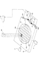
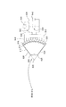
[0039]図1Aは本発明の1つの実施形態の等角図を図示し、この実施形態では、エネルギ源20が基板10の画定された領域またはアニーリング領域12上にある一定量のエネルギを投射することにより、アニーリング領域12内のある一定の所望の領域を優先的にアニーリングするようになっている。1つの実施形態では、図1Aに示されるとおり、アニーリング領域12などの基板の1つのみまたはそれ以上の画定された領域は任意の所定の時間にエネルギ源20からの放射線に曝露される。本発明の1つの態様では、基板10の単一範囲はエネルギ源20から送出される所望のエネルギ量に連続的に曝露され、基板の所望の領域の優先的なアニーリングを引き起こす。1つの例では、電磁放射源の出力に対して基板を平行移動する(例えば、従来のX/Yステージ、精密ステージ)ことにより、および/または基板に対して放射源の出力を平行移動することにより、基板の表面の1つの範囲が順次曝露される。典型的には、個別の精密ステージ(図示せず)の一部であってもよい、1つ以上の従来の電気アクチュエータ17(例えば、リニアモータ、リードスクリューおよびサーボモータ)を使用して、基板10の運動および位置を制御してもよい。基板10および熱交換デバイス15を支持し、位置合わせするために使用される従来の精密ステージは、カリフォルニア州ローナートパークのParker Hannifin Corporationから購入されてもよい。別の実施形態では、基板10の全体表面は一回で全て連続的に曝露される(例えば、アニーリング領域12の全体が連続的に曝露される)。
[0039] FIG. 1A illustrates an isometric view of one embodiment of the present invention in which an
[0040]1つの態様では、アニーリング領域12およびその領域に送出される放射線は、ダイ13(例えば40の「ダイ」が図1に示される)および基板の表面に形成される半導体デバイス(例えばメモリチップ)のサイズに整合するようなサイズとされる。1つの態様では、アニーリング領域12の境界は、各ダイ13の境界を画定する「切溝」または「けがき」線10A内に嵌まり込むように整列され、サイズ調節される。1つの実施形態では、アニーリングプロセスを実行する前に、基板の表面上に典型的に見られる整列マークおよび他の従来の技術を使用して、基板をエネルギ源20の出力に整列することにより、アニーリング領域12をダイ13に適切に整列できるようにする。アニーリング領域12が、けがき線または切溝線等のダイ13の間の自然に発生する未使用の空間/境界内でのみ重なり合うように、アニーリング領域12を連続して配置することは、デバイスが基板上に形成される範囲内のエネルギを重ね合わせる必要を低減し、これにより重なり合うアニーリング領域間のプロセス結果における変動を低減する。したがって、連続的に配置されるアニーリング領域12間に送出されるエネルギの重ね合わせは最小化されるので、基板の重要領域を処理するためにエネルギ源20から送出されるエネルギへの曝露量の変動に起因するプロセス変動の量は最小化される。1つの例では、連続的に配置されるアニーリング領域12の各々のサイズは、約33mm×約22mmの矩形の領域である(例えば、726平方ミリメートル(mm2)の面積)。1つの態様では、基板の表面上に形成される連続的に配置されるアニーリング領域12の各々の面積は約4mm2(例えば、2mm×2mm)から約1000mm2(例えば25mm×40mm)である。
[0040] In one aspect, the
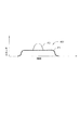
[0041]エネルギ源20は一般的に、基板表面のある一定の所望の範囲を優先的にアニーリングするために電磁エネルギを送出するようになっている。電磁エネルギの典型的な発生源は、光放射源(例えば、レーザ、フラッシュランプ)、電子ビーム源、イオンビーム源および/またはマイクロ波エネルギ源を含むが、これらに限定されない。1つの態様では、基板10は、1つ以上の適切な波長の放射線を放出するレーザから複数のパルスのエネルギに所望の期間曝露される。1つの態様では、エネルギ源20からの複数のパルスのエネルギを調節することにより、アニーリング領域12全体にわたって送出されるエネルギ量および/またはパルス期間内に送出されるエネルギ量を最適化して、基板表面上の領域を融解しないようにするが、アニーリングされる領域内の大部分のドーパントを制御可能に拡散し、且つアニーリングされる領域内の大きい量の損傷を、一度で、1つの格子平面または格子平面の小さなグループから除去することを制御して可能にするのみの十分なエネルギを送出するようにする。各パルスはマイクロアニーリング周期を完了し、高濃度範囲から低濃度範囲までの幾つかのドーパント拡散をもたらし、および非整列のアニーリング領域の底部近くの整列結晶の幾つかの格子平面のエピタキシャル成長をもたらす。1つの態様では、エネルギ源20の波長を調節して、放射線の大部分が基板10上に配置されたシリコン層により吸収されるようにする。シリコンを含む基板上で実行されるアニーリングプロセスでは、放射線の波長は約800nm未満であってもよく、深紫外線(UV)、赤外線(IR)または他の望ましい波長で送出されてもよい。1つの実施形態では、エネルギ源20は、レーザなどの高強度の光源であり、これは、約500nmから約11マイクロメートルの波長で放射線を送出するようになっている。別の実施形態では、エネルギ源20は、キセノン、アルゴンまたはクリプトン放電ランプ等の、複数の発光ランプを特徴とするフラッシュランプ配列である。幾つかの実施形態ではタングステンハロゲンランプもまた使用されるが、これらは、フィラメントを加熱および冷却する必要性によって、必要とされる短いパルスを生成するには十分に高速に点灯および消灯できないため、一般的に普及していない。したがって、タングステンハロゲンランプは、使用されるとき、パルスを管理するシャッタと共に使用されなければならない。また、タングステンハロゲンランプは一般的により低いエネルギ密度を送出し、したがってより多くのランプが必要とされる。全ての場合において、アニーリングプロセスにおいて使用されるエネルギパルスは一般的に、約1nsecから約10msecの程度の比較的短期間パルスで発生する。
[0041] The
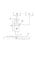
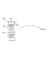
[0042]図1Bは図1Aの装置の概略側面図である。電源102はエネルギ源20に結合されている。エネルギ源20は、上述のような光源であってもよいエネルギ発生器104および光学アセンブリ108を備える。エネルギ発生器104はエネルギを発生し、そのエネルギを光学アセンブリ108に誘導するように構成され、この光学アセンブリにおいて、次に、基板10に送出するために所望とおりにエネルギを整形する。光学アセンブリ108は一般的にレンズ、フィルタ、ミラー等を備え、これらはエネルギ発生器104により発生されたエネルギを集束、偏光、偏光解消、濾波または可干渉性の調節を行うように構成され、アニーリング領域12に均一列のエネルギを送出する目的を有する。
[0042] FIG. 1B is a schematic side view of the apparatus of FIG. 1A. The
[0043]エネルギのパルスを送出するために、スイッチ106が提供されてもよい。スイッチ106は1μsecまたはそれ未満で開閉される高速シャッタであってもよい。あるいは、スイッチ106は、しきい値強度の光がこれに衝突すると1μsec未満以内に透明になる不透明結晶等の、光学スイッチであってもよい。幾つかの実施形態では、スイッチはポッケルスセルであってもよい。幾つかの実施形態では、光学スイッチは1nsec未満以内に状態を変えるように構成されてもよい。光学スイッチは、基板に誘導される電磁エネルギの連続ビームを遮断することによりパルスを生成する。スイッチは制御装置21により操作され、エネルギ発生器104の外側に設置されてもよく、例えば、エネルギ発生器104の出口範囲に結合または固定されてもよく、またはエネルギ発生器104の内部に設置されてもよい。代替の実施形態では、エネルギ発生器は電気的手段により切り替えられてもよい。制御装置21は、必要に応じて、電源102をオンおよびオフに切り替えるように構成されてもよく、または、制御装置21により駆動される回路によって電源102により充電され、およびエネルギ発生器104に放電するキャパシタ110が提供されてもよい。エネルギ発生器104は、キャパシタ110により提供される電気量がある一定の電力しきい値まで低下すると、エネルギを生成することを停止するため、キャパシタによる電気切換は自己切換式である。キャパシタ110が電源102により再充電されると、次にエネルギ発生器104に放電して、エネルギの別のパルスを生成することができる。幾つかの実施形態では、電気スイッチは1nsec未満で出力のオンまたはオフを切り替えるように構成されてもよい。
[0043] A
[0044]1つの実施形態では、アニーリングプロセスは活性化アニーリングステップとその後の連続パルスアニーリングプロセスとを含み、これにより所望のデバイス特徴を提供する。1つの実施形態では、活性化ステップは約1分の期間に約400℃から約800℃の温度に基板を加熱することを含んでもよい。別の実施形態では、活性化ステップは基板を事前加熱することを備える。 [0044] In one embodiment, the annealing process includes an activation annealing step followed by a continuous pulse annealing process, thereby providing the desired device characteristics. In one embodiment, the activation step may include heating the substrate to a temperature of about 400 ° C. to about 800 ° C. for a period of about 1 minute. In another embodiment, the activation step comprises preheating the substrate.
アニーリングプロセス中の基板の温度制御
[0045]1つの実施形態では、図1に図示されるとおり、基板10の表面を熱交換デバイス15の基板支持体面16に熱接触させて配置することによって、熱プロセス中に基板の温度を制御することが望ましい。熱交換デバイス15は一般的に、アニーリング処理に先立ってまたは処理中に、基板を加熱および/または冷却するように適合される。この構成では、カリフォルニア州サンタクララのApplied Materials, Inc.から市販されている従来の基板ヒータなどの熱交換デバイス15が、基板のアニーリングされる領域の処理後の特性を改善するために使用されてもよい。一般的に、基板10は、熱交換デバイス15を含む、処理チャンバ(図示せず)の密封処理環境(図示せず)内に配置されている。基板が処理中に存在する処理環境は排気されてもよく、または所望の処理に適したガスを含んでもよい。例えば、本発明の実施形態は、チャンバに提供されるある一定のガスを必要とする、堆積または埋込みプロセスにおいて使用されてもよい。ガスは、堆積プロセスに対する前駆体などの反応性、または、従来の熱プロセスにおいて通常使用される不活性ガスなどの非反応性であってもよい。
Temperature control of the substrate during the annealing process
[0045] In one embodiment, the temperature of the
[0046]1つの実施形態では、アニーリング処理を実行する前に基板を予熱し、これにより必要とされるアニーリングエネルギの増分を最小にしてもよい。これは、基板の迅速な加熱および冷却によって誘発される応力を低減し、また基板のアニーリング範囲内の欠陥密度を最小にできる場合がある。1つの態様では、熱交換デバイス15は、基板支持体面16上に配置された基板を加熱するように適合された、抵抗加熱素子15Aおよび温度制御装置15Cを含む。温度制御装置15Cは、制御装置21と通信する(以下に説明されている)。1つの態様では、約20℃から約750℃の温度に基板を予熱することが望ましい。基板がシリコンを含有する材料から形成されている1つの態様では、基板を約20℃から約500℃の間の温度に予熱することが望ましい。
[0046] In one embodiment, the substrate may be preheated before performing the annealing process, thereby minimizing the required increase in annealing energy. This may reduce stress induced by rapid heating and cooling of the substrate, and may minimize defect density within the annealing range of the substrate. In one aspect, the
[0047]別の実施形態では、アニーリングプロセス中に基板にエネルギを加えることによって、処理中の基板を冷却して相互拡散を低減することが望ましい。基板の融解の徐々な進行を必要とするプロセスにおいては、その後の冷却により再成長速度を増加してもよく、これにより、図8に関して説明されているとおり、処理中に様々な領域の非結晶化を増加できる。1つの構成では、熱交換デバイス15は、基板支持体面16上に配置される基板を冷却するように適合された、1つ以上の流体チャネル15Bおよび超低温冷却器15Dを含む。1つの態様では、制御装置21と通信する従来の超低温冷却器15Dが、1つ以上の流体チャネル15Bを介して冷却流体を送出するように適合されている。1つの実施形態では、約−240℃から約20℃の温度に基板を冷却することが望ましい。
[0047] In another embodiment, it is desirable to cool the substrate being processed to reduce interdiffusion by applying energy to the substrate during the annealing process. In processes that require gradual progression of substrate melting, subsequent cooling may increase the regrowth rate, which, as explained with respect to FIG. Can be increased. In one configuration, the
[0048]制御装置21(図1A)は一般的に、ここに説明されている熱プロセス技術の制御および自動化を促進するように設計されており、典型的に中央処理装置(CPU)(図示せず)、メモリ(図示せず)およびサポート回路(またはI/O)(図示せず)を含んでもよい。CPUは、様々なプロセスおよびハードウェア(例えば従来の電磁放射線検出器、モータ、レーザハードウェア)を制御するため、およびプロセスを監視(例えば基板温度、基板支持体温度、パルス化レーザからのエネルギ量、検出器信号)するために、工業環境において使用される任意の形式のコンピュータプロセッサの1つであってもよい。メモリ(図示せず)は、CPUに接続され、およびランダムアクセスメモリ(RAM)、読み出し専用メモリ(ROM)、フロッピーディスク、ハードディスクまたはローカルまたはリモートである任意の他の形式のデジタル記憶装置等の、1つ以上の容易に利用可能なメモリであってもよい。ソフトウェア命令およびデータはCPUに命令を与えるためにコード化されてメモリ内に格納される。サポート回路(図示せず)もまた従来の方法でプロセッサをサポートするためにCPUに接続される。サポート回路は従来のキャッシュ、電源、クロック回路、入力/出力回路、サブシステム等を含んでもよい。制御装置により読み取り可能であるプログラム(またはコンピュータ命令)は、いずれのタスクが基板に関して実行可能であるかどうかを決定する。好ましくは、プログラムは制御装置により読み取り可能なソフトウェアであり、基板位置、各電磁パルスで送出されるエネルギ量、1つ以上の電磁パルスのタイミング、各パルスに対する時間の関数としての強度および波長、基板の様々な領域の温度、およびこれらの任意の組み合わせを監視および制御するためのコードを含む。 [0048] Controller 21 (FIG. 1A) is generally designed to facilitate control and automation of the thermal process techniques described herein, and is typically a central processing unit (CPU) (not shown). ), A memory (not shown), and a support circuit (or I / O) (not shown). The CPU controls various processes and hardware (eg conventional electromagnetic radiation detectors, motors, laser hardware) and monitors the process (eg substrate temperature, substrate support temperature, amount of energy from pulsed laser) The detector signal) may be one of any type of computer processor used in an industrial environment. A memory (not shown) is connected to the CPU and includes random access memory (RAM), read only memory (ROM), floppy disk, hard disk or any other type of digital storage device that is local or remote, etc. There may be one or more readily available memories. Software instructions and data are encoded and stored in memory to provide instructions to the CPU. Support circuitry (not shown) is also connected to the CPU to support the processor in a conventional manner. Support circuitry may include conventional caches, power supplies, clock circuits, input / output circuits, subsystems, and the like. A program (or computer instructions) that can be read by the controller determines which tasks can be performed on the substrate. Preferably, the program is software readable by the controller, the substrate position, the amount of energy delivered with each electromagnetic pulse, the timing of one or more electromagnetic pulses, the intensity and wavelength as a function of time for each pulse, the substrate Code for monitoring and controlling the temperature of the various regions of and any combination thereof.
選択的加熱
[0049]形成されるデバイスの様々な領域間の相互拡散を最小にし、基板材料内の欠陥を除去し、基板の様々な領域内のドーパントをさらに均一に分散するために、基板の様々な領域上で1つ以上の処理ステップを実行して、それら領域が、アニーリングプロセス中にエネルギ源から送出されるエネルギに曝露されると優先的に融解されるようにしてもよい。アニーリングプロセスの間において、基板の第1領域および第2領域の両方がほぼ同一量のエネルギに曝露されるとき、第1領域の特性を改質して、第1領域が第2領域より優先的に融解されるようにするプロセスは、以後は、これらの2つの領域間に融解点コントラストを生成すると説明される。一般的に、基板の所望の領域を優先的に融解するように改質できる基板の特性は、基板の所望の領域内に1つ以上の元素を埋め込み、注入および/または同時堆積するステップと、基板の所望の領域に物理的損傷を生成するステップと、および基板の所望の領域に融解点コントラストを生成するように形成されるデバイス構造を最適化するステップと、を含む。これらの改質プロセスの各々は順番に再検討される。
Selective heating
[0049] Various regions of the substrate to minimize interdiffusion between the various regions of the formed device, remove defects in the substrate material, and more evenly distribute the dopant in the various regions of the substrate. One or more processing steps may be performed above so that the regions are preferentially melted when exposed to energy delivered from an energy source during the annealing process. During the annealing process, when both the first region and the second region of the substrate are exposed to approximately the same amount of energy, the properties of the first region are modified so that the first region takes precedence over the second region. The process of causing melting to occur is subsequently described as creating a melting point contrast between these two regions. In general, the properties of a substrate that can be modified to preferentially melt a desired region of the substrate include embedding, implanting and / or co-depositing one or more elements within the desired region of the substrate; Creating physical damage in a desired region of the substrate and optimizing a device structure formed to produce a melting point contrast in the desired region of the substrate. Each of these reforming processes is reviewed in turn.
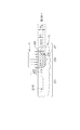
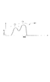
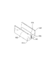
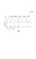
[0050]図2A〜図2Cは本発明の1つの実施形態を組み込んでいるデバイス製造シーケンスの各々の段階における電子デバイス200の断面図を図示している。図2Aは、MOSデバイスのソースおよびドレイン領域などの、2つのドープ領域201(例えばドープ領域201A〜201B)、ゲート215およびゲート酸化層216を有する基板10の表面205に形成される典型的な電子デバイス200の側面図を図示している。ドープ領域201A〜201Bは一般的に、基板10の表面205に所望のドーパント材料を埋め込むことにより形成される。一般的に、典型的なn型ドーパント(ドナー型の種)はヒ素(As)、リン(P)およびアンチモン(Sb)を含んでもよく、典型的なp型ドーパント(アクセプタ型の種)はホウ素(B)、アルミニウム(Al)およびインジウム(In)を含んでもよく、これらは、ドープ領域201A〜201Bを形成するために半導体基板10に導入される。図3Aは、ドープ領域201Aを通って延びる表面205から基板10内への経路203に沿って、ドーパント材料の濃度(例えば曲線C1)を深さの関数として示す例を図示している。ドープ領域201Aは、埋込みプロセス後に接合部の深さD1を有し、これは、ドーパントの濃度が無視できる量まで低下する点として定義されてもよい。図2A〜図2Eは単に、本発明の様々な態様の幾つかを図示することを目的としており、ここに説明されている本発明の様々な実施形態を使用して形成されてもよい、デバイスの種類、構造体の種類またはデバイスの領域を制限することを意図するものではないことに留意すべきである。1つの例では、ドープ領域201(例えばMOSデバイスにおけるソースまたはドレイン領域)は、ここに説明されている本発明の範囲から逸脱することなく、ゲート215(例えばMOSデバイスのゲート)の位置に対して上方または下方にあってもよい。半導体デバイスのサイズが減少すると、基板10の表面205上に形成される電子デバイス200の構造素子の位置および形状は、デバイスの製造性またはデバイスの性能を向上するために変化させてもよい。また、図2A〜2Eに示される単一のドープ領域201Aのみの改質は、本明細書に記載される本発明の範囲を制限することを意図するものではなく、単に、半導体デバイスを製造するために本発明の実施形態が使用される方法を図示することに留意すべきである。
[0050] FIGS. 2A-2C illustrate cross-sectional views of
[0051]図2Bは処理ステップ中の図2Aに示される電子デバイス200の側面図を図示しており、このステップは、この場合は単一ドープ領域201Aを含む領域である、基板10の個別の領域(例えば、改質される範囲210)の特性を選択的に改質することにより、融解点コントラストを生成するように適合される。改質プロセスを実行した後に、融解点コントラストは改質された範囲210と無改質の範囲211との間に生成される。1つの実施形態では、改質プロセスは、基板の表面上に材料を堆積するときに、その材料を層に追加するステップを含み、この場合、組み込まれる材料は基板材料との合金を形成して、改質される範囲210内の領域202の融解点を下げるように適合される。1つの態様では、組み込まれる材料は、エピタキシャル層堆積プロセス中に堆積される層に追加される。
[0051] FIG. 2B illustrates a side view of the
[0052]別の実施形態では、改質プロセスは、基板材料との合金を形成するように適合された材料を埋め込む(図2Bの「A」参照)ことにより、改質される領域210内で領域202の融解点を下げるステップを含む。1つの態様では、改質プロセスは図2Bに示されるとおり、深さD2に合金材料を埋め込むように適合される。図3Bは、ドーパント材料の濃度(例えば曲線C1)および埋め込まれた合金材料の濃度(例えば曲線C2)を、経路203に沿って表面205から基板10を通る深さの関数として図示している。1つの態様では、基板10はシリコン含有材料から形成され、使用されてもよい埋込み合金材料は、例えばゲルマニウム(Ge)、ヒ素(As)、ガリウム(Ga)、炭素(C)、スズ(Sn)およびアンチモン(Sb)を含む。一般的に、合金材料は、基板の基材が存在する状態で加熱されるとき、改質される範囲210内の領域202の融解点を無改質の範囲211と比較して低下させる、任意の材料であってもよい。1つの態様では、シリコン基板の領域を1%から約20%のゲルマニウムを添加することにより改質して、改質される範囲と無改質の範囲との間の融解点を低下させる。これらの濃度のゲルマニウムの添加により、改質された範囲の融解点を無改質の範囲に比べて約300℃下げると考えられている。1つの態様では、シリコン基板に形成される領域202はゲルマニウム(Ge)および炭素(C)を含み、これによりSixGeyCz合金を形成して、無改質の範囲211に比べて領域202の融解点を下げる。別の態様では、シリコン基板の領域は約1%以下のヒ素の添加により改質され、改質される範囲と無改質の範囲の間の融解点を低下させる。他の重要な合金は、ケイ化コバルト(CoxSiy、ただしyは一般的に約0.3xより大きく約3x未満である)、ケイ化ニッケル(NixSiy、ただしyは一般的に約0.3xより大きく約3x未満である)およびケイ化ニッケルゲルマニウム(NixGeySiz、ただしyおよびzは一般的に約0.3xより大きく約3x未満である)ならびに他のシリサイドおよび同様の材料を含むが、これら材料に限定されない。
[0052] In another embodiment, the modification process is performed in the
[0053]別の実施形態では、改質プロセスは、様々な改質される範囲(例えば改質される範囲210)内の基板10の材料に幾つかの損傷を与えて、基板の結晶構造体を損傷させることにより、これらの領域をより非結晶化するステップを含む。単一の水晶シリコン基板に損傷を与える等の、基板の結晶構造体の損傷を誘発することにより、基板の原子の結合構造の変化によって無傷の領域に比べてこの領域の融解点が低下し、その結果、2つの領域間の熱力学的特性の相違を誘発する。1つの態様では、図2Bにおける改質される範囲210への損傷は、基板の表面に損傷を生成できる投射物を用いて基板10の表面205(図2Bの「A」参照)に衝撃を加えることにより実行される。1つの態様では、投射物体はシリコン(Si)原子であり、このシリコンはシリコン含有基板に埋め込まれ、改質される範囲210内の領域202への損傷を誘発する。別の態様では、基板材料への損傷は、埋込みプロセスを使用して、アルゴン(Ar)、クリプトン(Kr)、キセノン(Xe)またはさらに窒素(N2)等のガス原子を用いて表面に衝撃を加えるか、または、イオンビームまたはバイアスプラズマ(biased plasma)によって生成され、改質される範囲210の領域202への損傷を誘発する。1つの態様では、改質プロセスは、図2Bに示されるとおり、深さD2まで誘発された損傷を有する領域202を生成するように適合される。約5×10¹⁴から約1×10¹⁶/cm2の転位または空位密度が、改質される範囲210と無改質の範囲211との間の融解点コントラストを生成するには有用である場合があると考えられている。1つの態様では、図3Bは、表面205から基板10を通る経路203に沿った、深さの関数としてドーパント材料の濃度(例えば曲線C1)および欠陥密度(例えば曲線C2)の例を図示している。
[0053] In another embodiment, the modification process may cause some damage to the material of the
[0054]図2A〜図2Bは、ドーピングプロセス後に改質プロセスが実行されるプロセスシーケンスを図示しており、このプロセスシーケンスは本明細書に記載される本発明の範囲を制限することを意図するものではない。例えば、1つの実施形態では、図2Aに説明されているドーピングプロセスを実行する前に、図2Bに説明されている改質プロセスを実行することが望ましい。 [0054] FIGS. 2A-2B illustrate a process sequence in which a modification process is performed after the doping process, which is intended to limit the scope of the invention described herein. It is not a thing. For example, in one embodiment, it may be desirable to perform the modification process described in FIG. 2B before performing the doping process described in FIG. 2A.
[0055]図2Cは、図2Bに示された電子デバイス200の側面図を図示しており、この電子デバイスはレーザからの光放射源などのエネルギ源から放射される放射線「B」に曝露される。このステップ中に、基板10全体にわたって配置された改質される範囲(例えば、改質される範囲210)および無改質の範囲(例えば211)は、ある一定量のエネルギに曝露され、放射線「B」のパルスが加えられた後に改質される範囲210内の領域202を選択的に融解および再凝固させるが、無改質の範囲211は凝固状態を維持する。エネルギ量、すなわちエネルギ密度および放射線「B」が加えられる期間を設定することにより、領域202の所望の深さと、領域202を生成するために使用される材料と、電子デバイス200を形成するために使用される他の材料と、形成される電子デバイス200内の構成要素の熱伝導特性とを知ることで、領域202を優先的に融解することができる。図2Cおよび3Cに示されるとおり、放射線「B」に曝露されると、領域202の再融解および凝固により、ドーパント原子(例えば曲線C1)および合金化原子(例えば曲線C2)の濃度は領域202内により均一に再分散されるようになる。また、領域202と基板バルク材料221との間のドーパント濃度は、鮮明に画定される境界(すなわち「アブラプト(hyper−abrupt)」接合)を有し、その結果、基板バルク材料211への不要な拡散を最小にする。上述の実施形態では、基板10内に損傷が誘発されて融解点コントラストを改善し、好ましくは、再凝固後の欠陥の濃度(例えば曲線C2)は無視できるレベルまで低下する。
[0055] FIG. 2C illustrates a side view of the
表面特性の改質
[0056]1つの実施形態では、基板10の様々な領域202全体にわたる表面の特性を変化させて、1つ以上の望ましい領域間の熱コントラストを生成する。1つの態様では、所望の領域における基板の表面の放射率を変化させて、処理中の基板表面により吸収されるエネルギ量を変更する。この場合、より高い放射率を有する領域は、エネルギ源20から受けるエネルギをより多く吸収できる。基板の表面の融解を含むアニーリングプロセスを実行するとき、基板の表面で得られる処理温度は極めて高く(例えば、シリコンの場合約1414℃)、放射熱伝達が主な熱損失メカニズムであるため、放射率の変化は熱コントラストに劇的な効果を与えることができる。したがって、基板表面の様々な領域の放射率の変化は、基板の様々な領域により到達される最高温度に著しい影響を有する場合がある。低い放射率を備える領域は、例えば、アニーリング処理中に融解点より高く温度が上がる場合があるが、同一のエネルギ量を吸収する高い放射率を備える領域は、融解点を大幅に下回る温度を維持する場合がある。この結果、基板表面は、放射源の波長における熱質量当たりの放射率はほぼ同一であるが全体的な放射率が異なる、領域を有してもよい。様々な表面の放射率または熱コントラストを変化させることは、基板表面に低いまたは高い放射率の被覆の選択的な堆積および/または基板の表面を改質すること(例えば、表面の酸化、表面の粗面処理)によって達成されてもよい。
Modification of surface properties
[0056] In one embodiment, the surface properties across the
[0057]1つの実施形態では、1つ以上の領域の基板の表面反射率を変化させて、基板10がエネルギ源からのエネルギに曝露されるときに吸収されるエネルギ量を変更する。基板表面の反射率を変化させることにより、基板の表面および下方における領域内の基板により吸収されるエネルギ量および得られる最大温度は、反射率によって異なる。この場合、より低い反射率を有する表面は、より高い反射率を有する別の領域より高い温度に達する。基板表面の反射率を変化させることは、基板表面に低反射率被覆または高反射率被覆を選択的に堆積および/または基板表面を改質すること(例えば、表面の酸化、粗面処理)によって達成されてもよい。高吸収性(非反射性)被覆は、アニーリングプロセス中により優先して加熱されることを目的としている領域に選択的に適用されてもよい。
[0057] In one embodiment, the surface reflectance of the substrate in one or more regions is varied to change the amount of energy absorbed when the
[0058]図2Dは、被覆225を選択的に堆積または均一に堆積して、基板10の表面205内の他の領域とは異なる放射率および/または反射率を有する層を残し、その後に選択的に除去される、1つの実施形態を図示している。この場合、被覆225の下方のドープ領域201A内の熱流(Q1)は、基板10の他の領域内で吸収されるエネルギ(Q2)に対して、被覆225の特性に基づいて調節できる。このようにして、熱損失(Q3)または被覆225から反射される熱は他の領域から失われる熱(Q4)に対して変化することができる。1つの態様では、炭素を含有する被覆が、CVD、PVDまたは他の堆積プロセスを使用して基板表面上に堆積される。
[0058] FIG. 2D selectively deposits or uniformly deposits the
[0059]図2Eは基板表面の光学特性(例えば放射率、反射率)を変化させる被覆226が、基板表面全体にわたり、例えば図2Aに示されるデバイス上に堆積され、次に材料のある一定量が除去されて異なる光学特性を有する領域を生成する、1つの実施形態を図示している。例えば、図2Eに示されるとおり、被覆226はゲート215の表面から除去され、その後に被覆226の表面を残し、ゲート215の表面は入射放射線「B」に曝露される。この場合、被覆226およびゲート215の表面は、異なる放射率および/または異なる反射率等の、異なる光学特性を有する。異なる光学特性を有する領域を曝露または生成するために使用される除去プロセスは、ウェットエッチングまたは化学機械研磨(CMP)プロセスなどの従来の材料除去プロセスの使用により実行される。この場合、被覆226の下方のドープ領域201A〜201B内の吸収および熱流(Q1)は、基板のゲート215領域における吸収および熱流(Q2)に対して被覆226の特性に基づいて調節される。この方法では、被覆226から失われるまたは反射される熱(Q3)はゲート215領域から失われるまたは反射される熱(Q4)に対して変化させることができる。
[0059] FIG. 2E shows that a
[0060]1つの実施形態では、被覆226は望ましい厚さの1つ以上の堆積層を含み、これらの層自体またはそれらの組み合わせのいずれかが入射放射線の1つ以上の波長に曝露される基板の様々な領域の光学特性(例えば、放射率、吸収率、反射率)を変更させる。1つの実施形態では、被覆226は層を含み、これらの層自体またはそれらの組み合わせのいずれかが入射放射線「B」の1つ以上の波長を優先的に吸収する。1つの態様では、被覆226は、ケイフッ化ガラス(FSG)、非晶質の炭素、二酸化ケイ素、炭化ケイ素、炭化ケイ素ゲルマニウム合金(SiCGe)、窒素を含有する二酸化ケイ素(SiCN)等の誘電材料、またはカリフォルニア州サンタクララのApplied Materials,Inc.から市販されているプロセスにより作られるBLOKTM誘電材料、または化学気相堆積(CVD)プロセスまたは原子層堆積(ALD)プロセスを使用して基板表面に堆積される炭素を含有する被覆を含む。1つの態様では、被覆226は、チタン(Ti)、窒化チタン(TiN)、タンタル(Ta)、コバルト(Co)またはルテニウム(Ru)等の金属を含むが、これらに限定されない。
[0060] In one embodiment, the
[0061]ここに説明されている様々な実施形態を相互に組み合わせて使用することにより、さらにプロセスの適用領域をさらに拡大してもよいことに留意すべきである。例えば、ある一定の画定された領域のドーピングに関して選択的に堆積される吸収被覆を使用し、アニーリングプロセスのプロセス適用領域を拡大してもよい。 [0061] It should be noted that the various embodiments described herein may be used in combination with each other to further expand the application area of the process. For example, an absorption coating that is selectively deposited with respect to the doping of certain defined areas may be used to expand the process application area of the annealing process.
優先的な加熱を達成するためのエネルギ源の出力調節
[0062]上述のとおり、エネルギ源20は一般的に、基板10のある一定の所望の領域を優先的に融解するために電磁エネルギを送出するようになっている。典型的な電磁エネルギ源は光放射源(例えばレーザ(UV、IR他の波長)、電子ビーム源、イオンビーム源および/またはマイクロ波エネルギ源を含むがこれらに限定されない。本発明の1つの実施形態では、エネルギ源20は、融解点に基板の所望の領域を選択的に加熱するために、レーザなどの光放射を送出するようになっている。
Adjusting the output of the energy source to achieve preferential heating
[0062] As described above, the
[0063]1つの態様では、基板10は1つ以上の適切な波長の放射線を放出するレーザからのエネルギのパルスに曝露され、放出される放射線は所望のエネルギ密度(W/cm2)および/またはパルス継続時間を有して、ある一定の所望の領域の優先的な融解を促す。シリコンを含有する基板上で実行されるレーザアニーリングプロセスでは、放射線の波長は典型的には約800nm未満である。いずれの場合も、アニーリングプロセスは一般的に、約1秒間またはそれ未満等の比較的短い時間で基板の所定の領域上でなされる。アニーリングプロセスにおいて使用される所望の波長およびパルスプロファイルは、基板の材料特性を考慮してレーザアニーリングプロセスの光学的および熱的モデリングに基づいて決定されてもよい。
[0063] In one aspect, the
[0064]図4A〜図4Dは、エネルギ源20からアニーリング領域12に送出されるエネルギのパルスの様々な属性(図1)は、時間の関数として調節され、これにより改善された熱コントラストおよびアニーリングプロセスの結果が得られる。1つの実施形態では、レーザパルスの形状を時間の関数として変化させ、および/または送出されるエネルギの波長を変化させることによって、融解を目的とする基板の領域への熱入力を強化し、他の領域への熱入力を最小にとどめることが望ましい。1つの態様ではまた、基板に送出されるエネルギを変化させることが望ましい場合がある。
[0064] FIGS. 4A-4D show that various attributes (FIG. 1) of the pulse of energy delivered from the
[0065]図4Aは、エネルギ源20から基板10に送出される(図1参照)、電磁放射線の単一パルス(例えばパルス401)の時間に対する送出されてもよいエネルギのグラフを図示している。図4Aに図示されるパルスは一般的に、全体パルス継続時間(t1)の間に一定のエネルギ量(E1)を送出する矩形パルスである。
[0065] FIG. 4A illustrates a graph of energy that may be delivered over time for a single pulse of electromagnetic radiation (eg, pulse 401) delivered from the
[0066]1つの態様では、パルス401の形状は基板10に送出されるとき、時間の関数として変化してもよい。図4Bは、1つのエネルギ源20から異なる形状を有する基板10に送出されてもよい、電磁放射線の2つのパルス401A、401Bのグラフを図示している。この例では、各パルスは、各曲線の下の面積により表わされるものと同一の総エネルギ出力を含んでもよいが、別のパルスに対比して1つのパルスに基板10の領域を曝露させる効果は、アニーリングプロセス中に生成される融解点コントラストを改善する場合がある。したがって、各パルスで送出される形状、ピーク出力レベルおよび/またはエネルギ量を調節することにより、アニーリングプロセスが改善されてもよい。1つの態様では、パルスはガウス形である。
[0066] In one aspect, the shape of the
[0067]図4Cは、台形の形状である電磁放射線パルス(例えばパルス401)を図示している。この場合、パルス401の2つの異なるセグメント(例えば402および404)では、送出されるエネルギは時間の関数として変化する。図4Cは、時間に対してエネルギが線形に変化している、パルス401のプロファイルまたは形状を図示しているが、これは、パルスで送出されるエネルギの時間変化が、例えば2次、3次または4次形状の曲線を有する場合もあるため、本発明の範囲を制限することを意図するものではない。別の態様では、時間の関数としてパルスで送出されるエネルギのプロファイルまたは形状は2次、3次または指数関数曲線であってもよい。別の実施形態では、処理中において、異なる形状(例えば、矩形および三角形の変調パルス、正弦波および矩形の変調パルス、矩形、三角形および正弦波の変調パルス等)を有するパルスを使用して、所望のアニーリング結果を得ることが有利な場合もある。
[0067] FIG. 4C illustrates an electromagnetic radiation pulse (eg, pulse 401) that is trapezoidal in shape. In this case, in two different segments of the pulse 401 (
[0068]デバイスの様々な領域の特性に応じて、電磁放射線の送出パルスの形状を調節することにより、アニーリング処理結果を改善してもよい。図4Bを参照すると、例えば、状況によっては、すなわちアニーリングプロセス中に加熱される基板の様々な領域が、低熱伝導率を有する範囲によりデバイスの他の領域から熱的に分離されている状況では、パルス401Bと類似の形状を有するパルスの使用が有利な場合もある。長い継続時間を有するパルスが有利なことも。この理由は、基板のより高い熱伝導性を有する材料領域は、伝導により熱を放散するためのより多くの時間を有し、一方で、アニーリングされる領域が熱的により十分に分離され、この結果、それらアニーリングされる領域においてより高い温度が発生するためである。この場合、パルスの継続時間、ピーク出力レベルおよび総エネルギ出力を適切に選択して、アニーリングを目的としない範囲が低温に維持されるようにする。パルスの形状を調節するプロセスもまた、変化する放射率を有する表面を使用して融解点コントラストを生成する場合に有利である。
[0068] Annealing process results may be improved by adjusting the shape of the delivery pulses of electromagnetic radiation according to the characteristics of the various regions of the device. Referring to FIG. 4B, for example, in some situations, i.e., where various regions of the substrate that are heated during the annealing process are thermally separated from other regions of the device by ranges that have low thermal conductivity. It may be advantageous to use a pulse having a shape similar to
[0069]図4Cを参照すると、1つの実施形態では、セグメント402の傾斜、パルス401の形状、セグメント403の形状、出力レベルにおける時間(エネルギレベルE1におけるセグメント403)、セグメント404の傾斜および/またはセグメント404の形状はアニーリングプロセスを制御するために調節される。粒子およびプロセス結果が変動する問題に起因して、アニーリングされる領域内の材料が処理中に蒸発することは一般的に望ましくないことに留意されるべきである。したがって、エネルギのパルス形状を調節することにより、領域を過熱して材料の蒸発を引き起こすことなく、アニーリングされる領域の温度を急速に目標温度にすることが望ましい。1つの実施形態では、図4Gに示されるとおり、複数のセグメント(すなわちセグメント402、403A、403B、403Cおよび404)を有するように調節されたパルス形状401を使用することにより、アニーリング領域を急速に目標温度にし、その後所望の期間(例えば、t1)にわたり材料をその温度に保持すると同時に、アニーリング領域内での材料の蒸発を防止する。時間の長さ、セグメントの形状およびパルスセグメントの各々の継続期間は、サイズ、融解深さおよびアニーリング領域内に含まれる材料が変化するに伴い、変化してもよい。
[0069] Referring to Figure 4C, in one embodiment, the slope of the
[0070]別の態様では、放射エネルギの複数の波長を組み合わせて基板の所望の領域へのエネルギ移送を改善することにより、熱コントラストの改善を達成し、および/またはアニーリングプロセス結果を改善してもよい。1つの態様では、組み合わされる波長の各々により送出されるエネルギ量を変更して、熱コントラストを改善し、およびアニーリングプロセス結果を改善する。図4Dはパルス401が2つの波長を含む1つの例を図示しており、このパルスはユニット当たり異なるエネルギ量を基板10に送出して、熱コントラストを改善し、および/またはアニーリングプロセス結果を改善してもよい。この例では、周波数F1がパルス時間内に一定レベルで基板に加えられ、別の周波数F2は、パルス期間中のある期間内にピークに達する部分を除いて、期間の大部分の間は一定レベルで基板10に加えられる。
[0070] In another aspect, improving the thermal contrast and / or improving the annealing process results by combining multiple wavelengths of radiant energy to improve energy transfer to a desired region of the substrate Also good. In one aspect, the amount of energy delivered by each of the combined wavelengths is changed to improve thermal contrast and improve the annealing process results. FIG. 4D illustrates one example where
[0071]図4Eは2つの異なる周波数F3およびF4でエネルギを送出する2つの連続セグメントを有するパルス401のグラフを図示している。したがって、基板の様々な領域は異なる波長において異なる割合でエネルギを吸収してもよいことから、図4Dおよび4Eに示されるとおり、可変エネルギ量を送出できる複数の波長を含むパルスを使用することは、望ましいアニーリング処理結果を得るのに有利である場合もある。
[0071] FIG. 4E illustrates a graph of a
[0072]1つの実施形態では、2つまたはそれ以上の電磁放射線のパルスを異なる時間で基板の領域に送出することにより、基板表面上の領域の温度を容易に制御できる。図4Fは、基板の表面上のある一定の領域を選択的に加熱するために、時間的に離れた変化する間隔すなわち周期(t)で送出される、2つのパルス401Aおよび401Bのグラフを図示している。この構成では、後続のパルス間の周期(t)を調節することにより、基板表面上の領域が到達するピーク温度を容易に制御できる。例えば、パルス間の周期(t)すなわち周波数を低下することにより、第1パルス401Aにおいて送出される熱は、第2パルス401Bが送出される前に放散する時間はより少なくなり、これにより、基板において達成されるピーク温度を、パルス間の周期が増加する場合より高くすることができる。この方法で周期を調節することにより、エネルギおよび温度を容易に制御できる。1つの態様においては、各パルス単独では、基板を目標温度に到達させるのに十分なエネルギを含まないが、パルスの組み合わせにより、領域202を目標温度に到達させることを保証することが望ましいこともある。2つまたはそれ以上のパルス等の、複数のパルスを送出するこのプロセスは、エネルギの単一パルスを送出することに対する、基板材料の受ける熱衝撃を低減する傾向がある。熱衝撃は基板の損傷につながり、基板に対して実行される後続の処理ステップにおいて欠陥を生成する粒子を発生させる可能性がある。
[0072] In one embodiment, the temperature of the region on the substrate surface can be easily controlled by delivering two or more pulses of electromagnetic radiation to the region of the substrate at different times. FIG. 4F illustrates a graph of two
[0073]図4Fを参照すると、1つの実施形態では、レーザなどの2つまたはそれ以上のエネルギ源を連続的に操作して、時間の関数として基板の表面の熱プロファイルを形成する。例えば、1つのレーザまたはレーザの配列はパルス401Aを送出して、基板の表面を時間T1の間に温度T0に上昇させてもよい。t1に先立ってまたは終了時に、第2パルス401Bが第2レーザからまたは連係して動作する複数のレーザから送出され、これにより、基板温度を時間t2の間に温度T1にする。このように、熱プロファイルは複数のレーザから送出されるエネルギの連続パルスを制御することにより形成することができる。このプロセスは、ドーパント拡散およびドーパント拡散の方向を制御する用途等の、熱プロセスの利点を有するが、これらに限定されない。
[0073] Referring to FIG. 4F, in one embodiment, two or more energy sources, such as lasers, are operated sequentially to form a thermal profile of the surface of the substrate as a function of time. For example, one laser or laser array may deliver a
電磁放射線パルス
[0074]シリコンを含有する基板または熱処理を必要とする別の材料から構成される基板の表面に十分な電磁放射線を送出する目的で、以下のプロセス制御が使用されてもよい。
Electromagnetic radiation pulse
[0074] The following process controls may be used for the purpose of delivering sufficient electromagnetic radiation to the surface of a substrate comprising silicon or another material that requires heat treatment.
[0075]1つの実施形態では、レーザなどの2つまたはそれ以上の電磁エネルギ源を連続的に操作して、熱処理される表面の熱プロファイルを形成する。この場合、レーザはパルス間のエネルギ変化を補正するような方法で操作される。1つの態様では、図1Aに概略的に図示されるエネルギ源20は、光放射源(例えばレーザまたはフラッシュランプ)、電子ビーム源、イオンビーム源および/またはマイクロ波エネルギ源等の、2つまたはそれ以上の電磁エネルギ源を含むが、これらに限定されない。パルスレーザなどのデバイスからのパルス間のエネルギは、各パルスの百分率変化を有する場合がある。パルスエネルギの変化は基板の熱プロセスでは許容されない場合がある。このパルス変化を補正するために、1つ以上のレーザは、基板の温度を上昇させるパルスを送出する。次に、送出されるパルスと、送出中のパルスのエネルギおよび立ち上がり時間とを監視するように適合された電子制御装置(例えば図1の制御装置21)を使用して、熱プロファイル(例えば、時間の関数として基板の領域の温度)を「トリミング」または調節するのに必要なエネルギ量を計算して、それがプロセス目標内にあり、第2のより小さいレーザまたは一連のより小さいレーザに命令を与えて、熱処理を完了するために最後のエネルギを送出するようにする。電子制御装置は一般的に、1つ以上の従来の放射線検出器を使用して、基板に送出されるパルスのエネルギおよび/または波長を監視する。小さいレーザはまたパルス出力エネルギのピーク間の変化を有してもよく、表面処理の開始時における最初のパルス(またはそれ以上のパルス)に比べてパルス当たり極めてに少ないエネルギを送出するため、この誤差は一般的にプロセス制限内にある。このように、電子制御装置は、パルスにより送出されるエネルギに変化を補償するように適合され、これにより、熱プロセス中に所望のエネルギレベルが送出されることを保証する。
[0075] In one embodiment, two or more electromagnetic energy sources, such as lasers, are operated sequentially to form a thermal profile of the heat treated surface. In this case, the laser is operated in such a way as to correct for energy changes between pulses. In one aspect, the
[0076]1つの態様では、上述の2つまたはそれ以上のエネルギ源はまた、色周波数の帯域幅、複数の波長、単一またはそれ以上の時間および空間レーザモード、および偏光状態を有するレーザ光のうちの単一色(波長)を使用して実現されてもよい。 [0076] In one aspect, the two or more energy sources described above may also include laser light having a color frequency bandwidth, multiple wavelengths, single or more time and space laser modes, and a polarization state. May be realized using a single color (wavelength).
[0077]1つ以上のレーザの出力は、基板表面に送出するための正確な空間および時間エネルギプロファイルを有していないことが多い。したがって、レーザの出力を形成するためにマイクロレンズを使用するシステムは、基板表面における均一な空間エネルギ分布を生成するために使用される。マイクロレンズのガラスの種類および形状を選択して、基板表面にパルスレーザエネルギを送出するために必要な光学系列における熱レンズ効果を補償してもよい。 [0077] The output of one or more lasers often does not have an accurate spatial and temporal energy profile for delivery to the substrate surface. Thus, a system that uses microlenses to form the output of the laser is used to generate a uniform spatial energy distribution at the substrate surface. The glass type and shape of the microlens may be selected to compensate for the thermal lens effect in the optical series required to deliver pulsed laser energy to the substrate surface.
[0078]スペックルとして知られている基板表面におけるパルスエネルギの高周波数変化は、入射エネルギの建設的および破壊的位相干渉の隣接領域により生成される。スペックルの補償は、1)基板における位相を急激に変化させるための表面音波デバイスが、この急激な変化が1つ以上のレーザパルスの熱処理時間より大幅に速くなるようにするステップと、2)レーザパルスのパルスを照射するステップと、3)レーザパルスの偏光を変化させ、例えば直線偏光されるが、非平行状態において偏光状態(eベクトル)を有する、複数の同時または遅延パルスを送出するステップと、を含んでもよい。 [0078] High frequency changes in pulse energy at the substrate surface, known as speckle, are generated by adjacent regions of constructive and destructive phase interference of incident energy. Speckle compensation includes: 1) a step in which the surface acoustic wave device for abruptly changing the phase in the substrate causes this abrupt change to be significantly faster than the heat treatment time of one or more laser pulses; Irradiating a pulse of a laser pulse; and 3) transmitting a plurality of simultaneous or delayed pulses that change the polarization of the laser pulse, eg, linearly polarized but have a polarization state (e-vector) in a non-parallel state. And may be included.
電磁放射線の送出
[0079]図5は、1つの実施形態における処理チャンバの領域の断面図であり、この実施形態では、エネルギ源20がある一定のエネルギ量を背面501から基板10のアニーリング領域12に送出して、アニーリング領域12内のある一定の所望の領域を優先的に融解するようになっている。1つの態様では、アニーリング領域12などの基板の1つ以上の画定された領域が任意の所定の時間においてエネルギ源20からの放射線に曝露される。1つの態様では、基板10の複数の範囲がエネルギ源20から背面501を通して送出される所望のエネルギ量に連続的に曝露されて、基板の所望の領域の優先的な融解を引き起こす。1つの態様では、アニーリング領域12のサイズは、基板10の上面502上に形成されるダイ(例えば図1Aのアイテム#13)または半導体デバイスのサイズと一致するようなサイズに調整される。1つの態様では、アニーリング領域12の境界は、各ダイの境界を画定する「切溝」または「けがき」線10A内に嵌まり込むように整列され、サイズ調節される。したがって、連続的に配置されたアニーリング領域12間の重複を最小にできることから、エネルギ源20からのエネルギへの曝露量の変化に起因するプロセス変化の量は最小化される。1つの例では、アニーリング領域12は約33mm×約22mmのサイズである矩形領域である。
Sending out electromagnetic radiation
[0079] FIG. 5 is a cross-sectional view of a region of a processing chamber in one embodiment, in which the
[0080]1つの実施形態では、基板10は、基板10の背面501がエネルギ源20から送出されるエネルギを受け入れることを可能にする開口512を有する、基板支持体510上に形成される基板支持領域511に位置合わせされる。基板10の背面に放射線を誘導する必要性が支持体510に開口を設けることを必要とする。本発明の他の実施形態はリング型基板支持体を必要としない。図5を参照すると、エネルギ源20から放出される放射線「B」は放出されるエネルギの一部を吸収するように適合された領域503を加熱する。エネルギ源20は、基板表面のある一定の望ましい領域を優先的に融解するように電磁エネルギを送出するようになってもよい。この実施形態では、電磁エネルギの典型的な発生源は、光放射源(例えばレーザ)および/またはマイクロ波、赤外線または近赤外線またはUVエネルギ源を含むが、これらに限定されない。1つの態様では、基板10は所望の期間内に1つ以上の適切な波長で放射線を放出するレーザからのエネルギのパルスに曝露される。1つの態様では、エネルギ源20からのエネルギのパルスを調節することにより、アニーリング領域12全体にわたり送出されるエネルギ量および/またはパルス期間内に送出されるエネルギ量を最適化して、ある一定の範囲の所望の熱処理を達成する。1つの態様では、レーザ波長を調節して、放射線の大部分が基板10上に配置されたシリコン層により吸収されるようにする。シリコンを含有する基板上で実行されるレーザアニーリングプロセスでは、放射線の波長は典型的には約900nmより長いが、深紫外線(UV)、赤外線(IR)または他の望ましい波長で送出されてもよい。いずれの場合でも、アニーリングプロセスは一般的に、約1秒間またはそれ未満等の、比較的短期間内に基板の所定の領域でなされる。
[0080] In one embodiment, the
[0081]1つの態様では、エネルギ源20からの放出放射線の波長を選択することにより、基板が形成されるバルク材料が、入射する放出放射線への曝露により加熱される上面502近傍の範囲に比べて入射放射線に対してより透過性であるようにする。1つの態様では、加熱される領域は、ドーパント材料や埋込みプロセス中に生成される結晶損傷(例えば、結晶欠陥、フレンケル欠陥、空間)を有する材料等の、基板の背面を通して送出されるエネルギ量を吸収する材料を含む。一般的に、ドーパント材料は、ホウ素、リンまたは半導体処理に使用される他の通常使用されるドーパント材料であってもよい。1つの実施形態では、基板が形成されるバルク材料集合体はシリコン含有材料であり、放出放射線の波長は約1マイクロメートルより長い。別の態様では、エネルギ源20は9.4から10.6マイクロメートル付近に中心を有する主波長域を放出するように適合されたCO2レーザを含む。さらに別の態様では、エネルギ源20は、一般的に約750nmから約1mmである、赤外線領域において波長を送出するようになっている。
[0081] In one aspect, by selecting the wavelength of the emitted radiation from the
[0082]1つの実施形態では、吸収被覆(図示せず)が基板10上のアニーリング領域12全体にわたって配置され、基板の背面を通して送出される入射放射線が基板を通過する前に吸収され得るようにする。1つの態様では、吸収被覆は、チタン、窒化チタン、タンタルまたは他の適切な金属材料等の、金属である。別の態様では、吸収被覆は、炭化ケイ素材料、非晶質の炭素材料またはドープダイヤモンド様炭素等の炭素を含有する材料または半導体デバイス製造に通常使用される他の適切な材料である。
[0082] In one embodiment, an absorbing coating (not shown) is disposed across the
[0083]1つの態様では、光の2つの波長が基板の所望する領域に送出される。このとき、光の第1波長は所望のアニーリング領域に見られるドーパントまたは他のイオン化結晶の損傷から基板内に自由キャリア(例えば、電子または正孔)を発生するために使用され、発生した自由キャリアは第2波長の基板の背面を通して送出されるエネルギを吸収する。1つの態様では、第1波長は、「緑色の光」の波長(例えば約490nmから約570nm)および/またはより短い波長である。1つの実施形態では、第1波長は、図5に示される、エネルギ源20から基板の反対側にある、第2のエネルギ源520から基板の所望の領域に、望ましい出力密度(W/cm2)で送出される。別の実施形態では、2つの波長(例えば、第1および第2波長)は、エネルギ源20から基板の背面を通して送出される。さらに別の実施形態では、望ましい出力密度(W/cm2)の2つの波長(例えば、第1および第2波長)は、電磁エネルギの2つの別個のエネルギ源(図示せず)から基板の背面を通して送出される。
[0083] In one aspect, two wavelengths of light are delivered to a desired area of the substrate. At this time, the first wavelength of light is used to generate free carriers (eg, electrons or holes) in the substrate from dopants or other ionized crystal damage found in the desired annealing region, and the generated free carriers Absorbs energy delivered through the backside of the second wavelength substrate. In one aspect, the first wavelength is a “green light” wavelength (eg, from about 490 nm to about 570 nm) and / or a shorter wavelength. In one embodiment, the first wavelength is the desired power density (W / cm 2) from the
パルス列アニーリング
[0084]次世代デバイスの製造の課題に対応するために、複数の電磁放射線のパルスを使用するアニーリングプロセスまたはパルス列アニーリングは幾つかのプロセスにおいて有用である。電磁放射線の複数の同一パルスは基板に送出され、各パルスは、1ミリ秒間(msec)以下の時間で基板表面の幾つかの原子層を準融解温度に近い温度(例えば、シリコン基板では約1300℃)まで加熱する単一マイクロアニーリングプロセスを達成し、その後、与えられたエネルギが結晶格子内で完全に消散し、影響を受けた格子層の温度が制御された予熱温度近くのより低い温度に戻ることを可能にする。予熱温度は、基板が第1パルスの送出の直前において維持される温度であり、約400℃から約800℃の間である。各マイクロアニーリングサイクルでは、結晶格子に結合されないシリコンおよびドーパント原子は、原子半径の数分の1程度で移動する。格子に結合されるシリコンおよびドーパント原子は、それらが送出されるパルスから十分なエネルギを受けないことから、一般的に移動しない。この方法では、各マイクロアニーリングサイクルは、所望の格子位置に個々の格子間原子およびドーパント原子を移動する。格子間原子またはドーパントが格子位置を満たすため、そのように位置を特定されない他の格子間原子またはドーパントは、結晶格子内の望ましい位置を見つけるまで、基板全体を通して拡散する。この方法では、パルス列アニーリング(以下「PTA」)を使用して、結晶格子内の格子間原子またはドーパントの原子の位置を制御でき、および過剰拡散を生じることなく、前の処理ステップ(例えば埋込みプロセス)の間に形成される格子欠陥を制御可能に修復することができる。このように、PTAは原子の長さ程度で半導体デバイス内の原子の運動を制御するために使用することができるプロセスである。
Pulse train annealing
[0084] An annealing process or pulse train annealing using multiple pulses of electromagnetic radiation is useful in several processes to address the challenges of next-generation device manufacturing. Multiple identical pulses of electromagnetic radiation are delivered to the substrate, and each pulse causes several atomic layers on the substrate surface to reach a temperature close to the semi-melting temperature (eg, about 1300 for a silicon substrate) in less than 1 millisecond (msec). A single micro-annealing process that heats up to 0 ° C.), after which the applied energy is completely dissipated in the crystal lattice and the temperature of the affected lattice layer is lowered to a lower temperature near the controlled preheating temperature Allows you to go back. The preheat temperature is the temperature at which the substrate is maintained just prior to delivery of the first pulse, and is between about 400 ° C. and about 800 ° C. In each micro-annealing cycle, silicon and dopant atoms that are not bonded to the crystal lattice move about a fraction of the atomic radius. Silicon and dopant atoms bonded to the lattice generally do not move because they do not receive enough energy from the pulse being delivered. In this method, each microannealing cycle moves individual interstitial atoms and dopant atoms to the desired lattice positions. Because the interstitial atoms or dopants fill the lattice position, other interstitial atoms or dopants that are not so located will diffuse throughout the substrate until the desired location within the crystal lattice is found. In this method, pulse train annealing (hereinafter “PTA”) can be used to control the position of interstitial atoms or dopant atoms in the crystal lattice, and prior processing steps (eg, embedded processes) without overdiffusion. ) Can be controlled in a controllable manner. Thus, PTA is a process that can be used to control the movement of atoms in a semiconductor device by as much as the length of the atoms.
[0085]図6Aは本発明の1つの実施形態によるプロセスを図示したフローチャートである。図6B〜図6Dはプロセス600の様々な段階における対象基板の特性を図示している。1つの実施形態では、基板は、基板表面に複数の電磁エネルギのパルスを送出することによりアニーリングされてもよく、各パルスは基板の少なくとも一部においてマイクロアニーリングプロセスを実行するように構成される。エネルギ放出は、レーザ、フラッシュランプおよびUVおよびマイクロ波源を含む、前述のエネルギ源の任意の集積により発生されてもよい。幾つかの実施形態では、エネルギ放出は上述のとおり短い継続時間のパルスの形を取り、各パルスの継続時間は約1nsecから約10msecの範囲である。各パルスは一般的に、例えば約10mWから10Wの間の、少なくとも10ミリワット(mW)の出力レベルで約0.2J/cm2から約100J/cm2のエネルギ密度で送出する。1つの実施形態では、例えば、各パルスにより送出されるエネルギ密度は約0.5J/cm2である。パルスに使用される光の波長を選択して、基板の結晶格子内の原子に最適な運動を引き起こすことができる。本発明の幾つかの実施形態において、エネルギのパルスは、赤外線スペクトル内にある波長で送出される。他の実施形態は、UVスペクトル内の光または異なるスペクトルからの波長を組み合わせた光を使用する。 [0085] FIG. 6A is a flowchart illustrating a process according to one embodiment of the invention. 6B-6D illustrate the characteristics of the target substrate at various stages of the process 600. FIG. In one embodiment, the substrate may be annealed by delivering multiple pulses of electromagnetic energy to the substrate surface, each pulse configured to perform a micro-annealing process on at least a portion of the substrate. The energy emission may be generated by any integration of the aforementioned energy sources, including lasers, flash lamps and UV and microwave sources. In some embodiments, energy release takes the form of short duration pulses as described above, with the duration of each pulse ranging from about 1 nsec to about 10 msec. Each pulse is generally sent for example between about 10mW of 10 W, at an energy density of from about 0.2 J / cm 2 to about 100 J / cm 2 at a power level of at least 10 milliwatts (mW). In one embodiment, for example, the energy density delivered by each pulse is about 0.5 J / cm 2 . The wavelength of light used for the pulse can be selected to cause optimal movement of atoms in the crystal lattice of the substrate. In some embodiments of the invention, pulses of energy are transmitted at a wavelength that is in the infrared spectrum. Other embodiments use light in the UV spectrum or light that combines wavelengths from different spectra.
[0086]理論により拘束されないことを意図して、PTAは、電磁放射線の複数のパルスを送出することにより基板内の原子の運動の原子レベルの制御を可能にすると考えられ、この場合、各パルスは完全なマイクロアニーリングサイクルを実行する。基板の表面に送出される、または表面により吸収される電磁放射線の各パルスは、基板表面または表面近傍に存在する原子にエネルギを提供する。送出されるエネルギは原子の運動を含み、幾つかの原子は格子内で位置を変える。原子を移動させるか、またはさせないかのいずれであっても、入射エネルギは全ての方向に、例えば基板の表面全体にわたり横方向に、および基板に垂直方向に、基板材料を通して伝達される。各パルスで送出されるエネルギは一般的に音波を生成し、この音波は、基板を通して伝搬するエネルギの波の特性を検出するように構成された、音波(例えば音声)検出器または光音波検出器等の検出器により検出できる。検出される特性は振幅、周波数および位相を含んでもよい。信号のフーリエ解析により、フィードバック制御に使用される高温測定方法と同様の監視プロセスを生み出してもよい。生の信号は、図1Aおよび1Bの制御装置21などの制御装置に提供されてもよく、制御装置は制御信号を発生して基板に送出されるエネルギを調節するように構成されてもよい。制御装置は各パルスへの電力入力、またはパルスの周波数または継続時間を調節してもよい。
[0086] Intended to be unconstrained by theory, PTA is believed to allow atomic level control of the motion of atoms in the substrate by delivering multiple pulses of electromagnetic radiation, where each pulse Performs a complete micro-annealing cycle. Each pulse of electromagnetic radiation delivered to or absorbed by the surface of the substrate provides energy to atoms present at or near the substrate surface. The energy delivered includes the movement of atoms, with some atoms changing positions within the lattice. Whether or not the atoms are moved, incident energy is transmitted through the substrate material in all directions, eg, laterally across the surface of the substrate and perpendicular to the substrate. The energy delivered with each pulse generally produces a sound wave, which is configured to detect the characteristics of the wave of energy propagating through the substrate, a sound wave (e.g. sound) detector or a photo wave detector. It can detect with detectors. The detected characteristic may include amplitude, frequency and phase. Fourier analysis of the signal may produce a monitoring process similar to the pyrometry method used for feedback control. The raw signal may be provided to a control device, such as the
[0087]本発明の実施形態は、基板の表面に電磁放射線のパルスを与えることにより結晶格子内に個々の原子の僅かな運動を優先的に引き起こす方法を提供する。上述のとおり、放射線は、基板表面の複数の領域に送出されるか、または基板の表面全体に同時に送出されてもよい。放射線の波長および強度は結晶格子内の個々の原子を対象にするように選択されてもよい。例えば、ドープされた単一結晶シリコン基板は大部分のシリコン原子の結晶格子を有し、幾つかのドーパント原子は格子間位置または結晶格子位置にある。幾つかの場合には、ドーパント濃度およびドーパントを埋め込むプロセスからの損傷結晶の濃度は過剰であってもよい。1つの実施形態では、電磁放射線のパルスは、格子の1つの平面から別の平面にドーパント原子運動の増分を引き起こすことにより、ドーパントおよび損傷結晶の局所的な濃度変化を補正するように設計されてもよい。強度および波長は、ドーパント原子の深さおよび所望の運動量に応じて調節されてもよい。使用されるエネルギの波長は一般的に、例えば、約3cmのマイクロ波から、可視波長を通り、例えば約150ナノメートル(nm)の深紫外線の範囲であってもよい。約300nmから約1100nmの範囲の波長は、例えば約800nm未満の波長等の、レーザ用途において使用されてもよい。より長い波長の効果は、基板の表面を照射する緑色の光を備えるキャリア放射線を提供することにより強化されてもよい。電磁放射線のパルスはまた、同様の方式で基板表面上に形成されるシリコン格子内のシリコン原子運動の増分を引き起こすように設計されてもよい。このような放射線の複数のパルスを送出することは、送出されるパルスの数に応じた程度の原子の制御可能な運動をもたらす。したがって、埋込みプロセスから表面損傷および範囲の末端損傷などの結晶格子の損傷を選択的に修復するステップと、および格子内のドーパント原子の局所的な濃度および分布を選択的に調節することが可能になる。 [0087] Embodiments of the present invention provide a method that preferentially causes a slight movement of individual atoms within a crystal lattice by applying a pulse of electromagnetic radiation to the surface of the substrate. As described above, the radiation may be delivered to multiple regions of the substrate surface or may be delivered simultaneously to the entire surface of the substrate. The wavelength and intensity of the radiation may be selected to target individual atoms within the crystal lattice. For example, a doped single crystal silicon substrate has a crystal lattice of most silicon atoms, with some dopant atoms in interstitial or crystal lattice positions. In some cases, the dopant concentration and the concentration of damaged crystals from the process of implanting the dopant may be excessive. In one embodiment, the pulse of electromagnetic radiation is designed to compensate for local concentration changes in the dopant and damaged crystals by causing an increase in dopant atomic motion from one plane of the lattice to another. Also good. The intensity and wavelength may be adjusted depending on the depth of the dopant atom and the desired momentum. The wavelength of energy used is typically in the range of, for example, from about 3 cm of microwave to visible wavelengths, for example deep UV of about 150 nanometers (nm). Wavelengths in the range of about 300 nm to about 1100 nm may be used in laser applications, such as wavelengths below about 800 nm. Longer wavelength effects may be enhanced by providing carrier radiation with green light that illuminates the surface of the substrate. The pulses of electromagnetic radiation may also be designed to cause an increment of silicon atomic motion in a silicon lattice formed on the substrate surface in a similar manner. Delivering multiple pulses of such radiation results in a controllable motion of the atom that depends on the number of pulses delivered. Thus, it is possible to selectively repair crystal lattice damage such as surface damage and range end damage from the embedding process, and to selectively adjust the local concentration and distribution of dopant atoms in the lattice. Become.
[0088]ステップ602では、レーザまたはフラッシュランプ放射などの電磁放射線のパルスを使用して基板を照射してもよい。パルスは10nsecから約20msec間の継続時間を有してもよい。基板表面に入射する各パルスにより結晶格子の振動が発生し、この振動が基板を通して伝搬する。パルスの間隔が十分長い場合、振動エネルギは結晶格子内で放散され、熱として放射される。基板の表面に約0.2J/cm2から約100J/cm2の間のエネルギ送出するパルスにより結晶格子内に与えられる振動エネルギは、熱として放散し、パルスの終了後に約1マイクロ秒間(μsec)以内に放射されてもよい。パルスの間隔が個々のパルスにより送出される熱を放散するのに必要とされる時間より短い場合、格子内に熱が蓄積され、格子の温度が上昇する。この状態は標準的な急速熱アニーリングまたはスパイクアニーリングに近く、この状態では、基板は基板の融解点を下回る温度まで加熱されるが、格子原子の拡散および再配列を可能にするには十分高い。従来の熱アニーリングプロセスでは、所望の拡散長さが極めて小さい(例えば僅か数ナノメートル)場合、原子の平均拡散長を制御するのに苦労している。現在の従来の急速熱アニーリング(RTA)システムは、約2.5秒間より長い期間にわたってエネルギを送出できるのみである、ランプおよびサポート回路を使用する。熱伝達時間、すなわち熱が基板の前面から背面に拡散するのに要する時間は20msec程度である。したがって、従来のRTAチャンバは、送出されるエネルギが基板全体を加熱して、基板の全ての範囲内のドーパントおよび他の原子の不要な拡散を引き起こすことから、45nmまたは32nmおよびより小さいノードデバイスに対しては拡散プロセスを適当に制御することができない。また、送出されるパルスの間隔が十分長い場合、各パルスの相加効果が基板温度を上昇させず、その結果、各パルスの熱効果は、パルスの継続時間および強度に応じて、基板の表面のすぐ下の範囲、例えば、表面から約100オングストロームまたはそれより下までの範囲に局所化される、と考えられている。各パルスは同一エネルギを送出することが好ましいが、幾つかの実施形態では、例えば所望のパターンを増加または減少する等の所定の方法に従って変化するエネルギを有するパルスを送出することが有利な場合がある。
[0088] In
[0089]幾つかの実施形態では、10nsecのパルスに続いて、基板表面にエネルギが送出されない(例えば「休止」時間)1msecまたはそれ以上の間隔があってもよい。図10に示されるとおり、1つの実施形態では、一連のパルス1000が送出されることが望ましい。この実施形態では、大きさE1および継続時間t1を有する電磁エネルギの単一パルスまたはパルス1001が基板表面に送出され、続いて、基板表面にエネルギが送出されない継続時間t2を有する「休止」期間1002があり、その後に次のパルス1001が受け取られる。1つの実施形態では、継続時間t1は、約1msecから約10msecの間であり、継続時間t2は約1msから20msの間である。1つの実施形態では、アニーリングプロセスの間に送出される各パルス1001は同一パルス継続時間内に同一量の総エネルギを送出する。図10を参照すると、エネルギ1001の単一パルスは方形波パルスとして示されるが、この形状は、本明細書に記載される本発明の範囲を制限することを意図するものではない。なぜなら、送出されるエネルギの形状は三角形、ガウス形、または任意の他の望ましい形状であり得るからである。
[0089] In some embodiments, a 10 nsec pulse may be followed by an interval of 1 msec or more during which no energy is delivered to the substrate surface (eg, a “pause” time). As shown in FIG. 10, in one embodiment, it is desirable that a series of
[0090]温度または温度勾配の従来の定義は、小数の格子平面または原子のみが短いエネルギパルスにより影響を受けることから、45nmおよび32nmデバイスノードに対しては所望のアニーリングの深さにおけるそれら温度の意味を失うことに留意すべきである。本発明による電磁放射線のパルスを受ける基板の表面近傍の局所的な温度は、結晶格子内の小数の原子の振動により生じるとき、300℃から1400℃に瞬間的に上昇する場合がある。他の実施形態では、フラッシュランプからの光パルスが使用されてもよく、ここでは、約0.2J/cm2から約100J/cm2の間のエネルギパルスが約10nsecから約10msecの期間内に送出されてもよい。 [0090] The conventional definition of temperature or temperature gradient is that only a small number of lattice planes or atoms are affected by short energy pulses, so for 45 nm and 32 nm device nodes, the temperature of those temperatures at the desired annealing depth. It should be noted that it loses its meaning. The local temperature in the vicinity of the surface of the substrate that receives the pulse of electromagnetic radiation according to the present invention may increase instantaneously from 300 ° C. to 1400 ° C. when caused by the oscillation of a small number of atoms in the crystal lattice. In other embodiments, light pulses from a flash lamp may be used, where energy pulses between about 0.2 J / cm 2 and about 100 J / cm 2 are within a period of about 10 nsec to about 10 msec. It may be sent out.
[0091]図6Bはドープ領域113を有する基板を図示している。埋込みの直後およびアニーリングの前には、ドープ領域113はドーパント原子またはイオン650の埋め込み層を有する。この層は、イオンを埋め込むプロセスにより生成され、一般的に結晶格子内の原子分布を生成し、原子の最高濃度が基板の表面近傍にあり、基板内のより深い部分の濃度はより低くなる。層650は領域113内の最高ドーパント濃度の位置を表す。領域113は埋込みに先立って非晶質化されている場合、埋込層650のすぐ上および下の領域113の層は非晶質状態であってもよい。領域113が埋込みに先立って非晶質化されていない場合、領域113のすぐ下の層は実質的に整列結晶格子であるのに対して、埋込み層650のすぐ上の領域113の層は結晶格子構造を通るドーパント原子の強制的な通過により生じる多数の結晶欠陥を呈する。いずれの場合でも、アニーリングの目的は、領域113の結晶構造体を再整列し、結晶格子の正規の位置に領域113全体にわたってドーパント原子を分散し、領域113の格子構造を再結晶化または整列することである。このようなアニーリングはドーパント原子を活性化し、領域113に適切に電子または正孔を供給し、格子欠陥から生じる領域113の抵抗を低下させる。
FIG. 6B illustrates a substrate having a doped
[0092]幾つかの実施形態では、複数のパルスを使用して結晶格子内において所望の効果を得る。10から100,000の数の複数のパルスを使用して、ほぼ単一の格子平面またはほぼ1つの原子間距離から、多数の格子または多数の原子間距離までの範囲の原子の運動を発生してもよい。1つの実施形態では、約30から約100,000のパルスの間の少なくとも30のパルスを使用して基板をアニーリングする。別の実施形態では、約50から約100,000のパルスの間の少なくとも50のパルスを使用して基板をアニーリングする。別の実施形態では、約70から約100,000のパルスの間の少なくとも70のパルスを使用して基板をアニーリングする。別の実施形態では、約100から約100,000のパルスの間の少なくとも100のパルスを使用して基板をアニーリングする。別の実施形態では、約10,000から約70,000パルスの間の約50,000のパルスを使用して基板をアニーリングする。パルスの数は一般的に、アニーリングプロセスが終点(それ以上アニーリングが実施されない点)に到達することから、約100,000未満である。上述のとおり、各パルスは完全なマイクロアニーリングサイクルを達成する。各パルスは単に、個々の格子平面の分離距離より短い距離で幾つかのドーパントまたはシリコン原子の運動を引き起こすのに十分強力であり、この結果、活性化の僅かな増分または結晶修復をもたらせてもよい。パルスエネルギを基板内で完全に放散させることにより、次のパルスの照射の前に原子の運動を停止させる。この方法でパルスの数を調節することにより、結晶格子内の原子の拡散および再配列の制御が可能になる。 [0092] In some embodiments, multiple pulses are used to achieve a desired effect in the crystal lattice. A number of pulses from 10 to 100,000 are used to generate motion of atoms ranging from approximately a single lattice plane or approximately one interatomic distance to many lattices or many interatomic distances. May be. In one embodiment, the substrate is annealed using at least 30 pulses between about 30 and about 100,000 pulses. In another embodiment, the substrate is annealed using at least 50 pulses, between about 50 and about 100,000 pulses. In another embodiment, the substrate is annealed using at least 70 pulses between about 70 and about 100,000 pulses. In another embodiment, the substrate is annealed using at least 100 pulses, between about 100 and about 100,000 pulses. In another embodiment, the substrate is annealed using about 50,000 pulses between about 10,000 and about 70,000 pulses. The number of pulses is generally less than about 100,000 because the annealing process reaches the end point (the point where no further annealing is performed). As described above, each pulse achieves a complete micro-annealing cycle. Each pulse is simply powerful enough to cause some dopant or silicon atom motion at distances shorter than the separation distance of the individual lattice planes, resulting in a slight increment of activation or crystal repair. May be. By completely dissipating the pulse energy within the substrate, the movement of the atoms is stopped before the next pulse irradiation. By adjusting the number of pulses in this way, it is possible to control the diffusion and rearrangement of atoms in the crystal lattice.
[0093]基板の表面における入射電磁放射線の効果は格子内の原子に運動エネルギを与えることであり、放射線は基板を通して伝達される。本発明の別の実施形態は、格子振動の音響結果を検出することにより、基板上の放射線の効果を監視することを提供する。図6Cおよび図6Aのステップ604は、基板100から放射する音波652により表わされる、基板の音響応答を監視することを図示している。音響応答は、振動エネルギが基板において吸収される度合いを表示し、これはドーパントおよび格子間に位置する原子の運動に関する幾つかの情報を提供する。格子秩序が増加すると、格子欠陥は減少し、原子の再分散は減少し、基板の音響応答は、入射エネルギを吸収する傾向からより多くのエネルギを伝達する傾向に変化する場合がある。このように、終点はステップ606において検出されてもよく、この終点を超えるとほとんどアニーリングが発生しない。1つの実施形態では、処理チャンバ内に音波検出器654を配置することにより、電磁放射線パルスが格子内に音波を生成するとき、基板の音響応答の音を測定する。この場合、音波検出器654を基板の表面に隣接して位置合わせして、電磁エネルギパルスの送出により生成される音波を検出するようにしてもよい。
[0093] The effect of incident electromagnetic radiation on the surface of the substrate is to impart kinetic energy to the atoms in the lattice, and the radiation is transmitted through the substrate. Another embodiment of the invention provides for monitoring the effect of radiation on the substrate by detecting the acoustic result of the lattice vibration. Step 604 of FIGS. 6C and 6A illustrates monitoring the acoustic response of the substrate, represented by
[0094]別の実施形態では、図6Eに概略的に図示されるとおり、チャンバ内に光音波検出器を配置して、入射電磁パルスにより基板の表面から反射する光ビーム上に誘発される音波を測定してもよい。幾つかの実施形態では、音響応答は、パルスが送出される基板の同一表面から測定されてもよく、幾つかの実施形態では、基板がウェハである場合、基板の異なる面(例えば、反対側)上で測定されてもよい。図6Eは、1つの実施形態に従って電磁エネルギのパルスが基板表面に送出されるとき、基板100上の音響応答を検出するのに使用される光音波検出器を図示している。放射源656は、基板100のデバイス側に向かって低出力電磁エネルギ660Aを放射し、検出器658は反射された放射線660Bを受け取る。基板100により受け取られる電磁パルスは基板100の表面の短い継続時間の変位をもたらし、これは次に、反射エネルギ660Bに影響を与える。次にこの反射光を検出器658により検出し、分析し、アニーリングの進行に伴い受け取られたエネルギに対する基板100の応答の変化量を監視するために分析してもよい。結晶構造が変化するとき、基板の音響応答が変化し、終点は図6Aのステップ606において検出されてもよい。図6Fは基板の背面から音響効果を監視する光音波検出器の代替の実施形態である。同様に検出器を採用して、任意の表面または側面および任意の好適な角度からの基板の反射率、透過率または吸収率の変化を検出してもよい。
[0094] In another embodiment, as schematically illustrated in FIG. 6E, a photoacoustic detector is disposed within the chamber to induce acoustic waves on the light beam reflected from the surface of the substrate by incident electromagnetic pulses. May be measured. In some embodiments, the acoustic response may be measured from the same surface of the substrate on which the pulse is delivered, and in some embodiments, if the substrate is a wafer, a different side of the substrate (eg, the opposite side) ) May be measured above. FIG. 6E illustrates a photoacoustic detector used to detect an acoustic response on the
[0095]他の実施形態では、前処理プロセスステップにおいて低エネルギパルスを使用して、所望の格子修復およびドーパントの再構成を達成するのに必要なエネルギ量を決定するのに役立ててもよい。このプロセスシーケンスは図7A〜図7Eに図示される。ステップ702では、低エネルギパルスは図7Bに図示されるとおり、基板の表面上に誘導される。パルス750の強度は、基板100のドープ領域113をアニーリングするのに必要な強度よりかなり小さい強度であってもよい。パルス750は、基板における音響応答を生成し、この応答はステップ704において監視され、記録されてもよい。音波検出器752は、図7Cに図示されるとおり、基板からの音響応答を記録するように配置されてもよい。ステップ706では、音響応答の解析は、アイテム754により図7Cにおいて概略的に表わされているアナライザにより実行されてもよい。アナライザ754はコンピュータを備えてもよく、このコンピュータは音波信号を受け取り、信号を検査し、解析し(すなわち信号の意味のあるパターンを強調する)、また受け取ったエネルギが所望の範囲内にない場合、以後のパルスのエネルギの制御またはオペレータへの警告などの幾つかの出力を提供するように構成される。パルス750は基板100をアニーリングしないが、音響応答は、アニーリングに必要とされるエネルギパルスの正確な特性を示す検出可能な特徴を有する。上述のとおり、より大きい結晶の非整列またはより深い領域の非整列を有する基板は、より大きな入射エネルギを吸収および放散し、より大きな結晶の整列を有する基板はより大きな入射エネルギを伝達し、様々な音響応答を生み出す。解析により、ステップ708において送出されるパルス756に最適な強度および数(図7D)を明らかにして、所望の結果を達成することができる。ステップ710において、第2グループのパルスの送出が監視され、任意選択的に終点検出712により達成されてもよい。終点が図6Aおよび7Aにおいて到達された後、領域113は最適にアニーリングされ、埋込み層650はドーパントが結晶格子に組み込まれると消滅する。
[0095] In other embodiments, low energy pulses may be used in the pre-processing process steps to help determine the amount of energy required to achieve the desired lattice repair and dopant reconstruction. This process sequence is illustrated in FIGS. 7A-7E. In
フラッシュランプ装置
[0096]図8Aは本発明の1つの実施形態による装置を図示している。八角形の外壁802を有する本体部分800が設けられている。本体部分800の第1端810は基板ホルダ804に結合されている。基板ホルダ804は、基板の装着および取外しを可能にするように構成される、ヒンジ形蓋をまたは基板を交換するための側面開口を備えてもよく、どちらも図8Aまたは8Bには示されていない。基板は基板ホルダ804を使用して所定の位置に保持されてもよく、このホルダは静電手段、真空手段、クランプ、ベルヌーイチャッキング、空気浮上、ピン支承、または音響手段により操作されてもよい(これらは図示されていない)。図8Bを参照すると、反射ライナ806が本体部分800の外壁802の内面上に配置されてもよい。好ましくは、基板ホルダ804は、本体部分800と実質的に半径方向に整列する位置に基板808を保持するように構成され、これにより基板808の最も均一な照射を支援する。基板ホルダ804は任意の向きまたは状態に基板808を保持するように構成されてもよく、これには、実質的に平らな向きまたは凸状または凹状の湾曲部などの変形された向きを含む。基板ホルダ804はまた、処理中に基板808に熱エネルギを送出することにより、基板808のバルク温度を制御するように構成されてもよい。このような熱エネルギは、基板の背面に接触する基板ホルダ804の表面を加熱または冷却することにより送出されてもよい。加熱または冷却は、基板ホルダを通して加熱または冷却流体を循環する等の、当業者には公知の手段により達成されてもよい。バックグラウンドまたはバルク熱エネルギはまた、加熱ランプ、冷却ガス等等の任意の従来の非接触手段により送出されてもよい。例えば、基板808は、基板808と基板ホルダ804との間が接触しないように、基板808にクッションを提供する冷却ガスを用いて、静電力または空気圧または真空によって所定の位置に保持されてもよい。基板808は個別にまたは基板ホルダ804と組み合わせて、例えば磁気的結合または機械的回転によって、回転エネルギを受けてもよい。
Flash lamp device
[0096] FIG. 8A illustrates an apparatus according to one embodiment of the invention. A
[0097]再度図8Aを参照すると、放射アセンブリ812は本体部分800の第2端814に結合されている。放射アセンブリ812は、フラッシュランプから広帯域アニーリング電磁エネルギを本体部分800に誘導し、次にエネルギを基板808上に誘導するようにして、複数のフラッシュランプを収容して構成される。図8Cを参照すると、放射アセンブリ812の側面図が図示されており、トラフ反射体818内に収容された複数のフラッシュランプ816が示される。トラフ反射体818は放射アセンブリ812の後面820に沿って並べられている。後面820は、放射アセンブリ812の側壁824から延びる線が交わる点822に中心を置く円弧を近似するように構成される。放射アセンブリ812は、側壁824、後面820、およびトラフ反射体818を覆う反射ライナ826を有してもよい。放射アセンブリ812はまた、レンズ開口830内に配置されるレンズ828を有して、放射アセンブリ812から、電磁エネルギを本体部分800を通して基板808上に誘導してもよい。レンズ828は、平坦または凸状または凹状の表面を有する、単レンズまたは複合レンズであってもよい。レンズ828はまたフレネルレンズであってもよく、また網目状、縞状または切子面状であってもよい。レンズ828は、放射アセンブリ812のレンズ開口830と本体部分800の第2端814との間の接合部を占有する。幾つかの実施形態では、2つ以上のレンズが使用されてもよい。他の実施形態では、放射アセンブリ812はフラッシュボックスであってもよい。
[0097] Referring again to FIG. 8A, the radiating
[0098]図8Dはレンズ開口830(図8C)を通して見られる放射アセンブリ812を図示している。フラッシュランプ816およびトラフ反射体818は放射アセンブリ812の後面820上に見ることができる。この透視図はまた後面820の円弧の形を図示している。図8Eは本発明の1つの実施形態による1つのトラフ反射体およびフラッシュランプアセンブリの等角図である。フラッシュランプ816は円柱形状であってもよく、トラフ反射体818内に配置されてもよい。散乱によるエネルギ損失を最小にするために、トラフ反射体818の断面を放物線状にしてもよい。フラッシュランプ816は電極832により電力を供給され、支持体850によりトラフ反射体から間隔を空けている。各フラッシュランプは別個の電源により電力を供給されてもよく、フラッシュランプ群をまとめて、単一電源により電力を供給してもよい。反射ライナ826は、放射された光がトラフ反射体818内に反射し、レンズ828に向かって放射アセンブリ812内に戻るのを容易にする。図8Fは本発明の別の実施形態によるトラフ反射体852の等角図である。トラフ反射体852は一般的に、トラフの中心の下方の突出部854を除いて、図8Eのトラフ反射体818と同一の構成要素を特徴とする。突出部はフラッシュランプ816から発散する光をランプから離れる方向に反射するように送り、これにより、反射光がランプ816を通って逆に進まないようにするのに役立つ。1つの実施形態では、突出部854は伸開線を形成し、内旋状の放物線プロファイルを有するトラフ反射体852をもたらす。他の実施形態では、トラフ852は特定の方向に反射光を誘導するように構成される内旋状の不規則プロファイルを有してもよい。
[0098] FIG. 8D illustrates the
[0100]図8Cを再度参照すると、放射アセンブリ812に結合されて、フラッシュランプ816に電力を供給する電力システムが示される。充電回路836および点灯回路838に結合されたキャパシタ834が示される。このように、キャパシタはスイッチ840を使用して充電および放電できる。電源842はキャパシタ834を充電するために示され、制御装置844はスイッチを操作するために示される。スイッチ840はキャパシタ834を充電および放電するために制御装置844により操作されてもよい。フラッシュランプ816は点灯リード848により電力を供給される。点灯リード848の長さが異なるためにフラッシュランプ816への不均一な電力送出および最適ではないフラッシュタイミングをもたらす場合があることから、分電装置846を通して放電キャパシタ834を放電するのが有利である。分電装置846は、必要に応じて、点灯リード848を通してフラッシュランプ816に送出される電力を平衡化する。簡略化するために、単一組の充電およびファイヤリング回路が図示されるが、上述のとおり、複数の回路を使用して1つ以上のフラッシュランプ816を放電してもよい。より多くの回路を使用することはフラッシュランプ816に対してファイヤリングパターンの最適化を容易にし、毎回全てのランプを点灯することなく装置の操作を可能にすることによりフラッシュランプの耐用年数を延ばす。同様に、複数のキャパシタを並列に使用して大きな電荷を充電および放電することを可能にしてもよく、複数の回路を追加して採用することにより、フラッシュランプに使用するパルス列を生成してもよい。最終的に、点灯回路に選択的にインダクタ(図示せず)を含むことにより、フラッシュランプ816を通して放電される電力パルスの形状を調節してもよい。小電流でフラッシュランプを事前にイオン化するための回路(図示せず)を使用して、放射アセンブリのフラッシュランプの出力を調節してもよい。
[0100] Referring again to FIG. 8C, a power system coupled to the radiating
[0101]1つの実施形態では、複数のフラッシュランプが放射アセンブリ812などの放射アセンブリ内に配置される。幾つかの実施形態では、複数のフラッシュランプは2つのフラッシュランプ群を備え、各群は図8Dに示される実施形態と同様に構成される。1つの実施形態では、2つのフラッシュランプ群を備え、各群は図8Dに示される実施形態と同様に構成される。1つの実施形態では、複数のフラッシュランプは2つのフラッシュランプ群を備え、フラッシュランプの各群は18のフラッシュランプを備える。幾つかの実施形態では、複数のフラッシュランプは、図8Cの1つのランプからレンズ828に引かれた線が別のランプに影響を与えないように、千鳥構成を備える群に構成されてもよい。別の実施形態では、フラッシュランプは高密度の平坦な線形配列を備えてもよい。フラッシュランプは放物線状の反射体トラフ、内旋状の放物線状の反射体トラフ、内旋状の不規則な反射体トラフ、またはこれらの任意の組み合わせで配置されてもよい。他の実施形態では、3つ以上のフラッシュランプ群が使用されてもよい。
[0101] In one embodiment, a plurality of flash lamps are disposed within a radiation assembly, such as
[0102]図9Aはフラッシュランプ装置900の代替の実施形態を図示している。本体部分902は一端に基板ホルダ904を、他端に放射領域を備えている。放射領域906は本体部分902の内部範囲の全体にわたり配置されたフラッシュランプ908を特徴とする。各フラッシュランプ908は本体部分902の少なくとも1つの側面(例えば2つが示される)を貫通するように構成される。本体部分902の断面は、六角形、八角形、正方形または任意の有利な形状であってもよい。フラッシュランプは本体部分902の側面の各対につき1つ配置されてもよく、または側面の各対につき2つ以上のフラッシュランプが配置されてもよい。フラッシュランプ908は、本体部分内での間隔の不一致を回避するために、本体部分902の長さに沿って長手方向に間隔を空けてもよい。代替として、フラッシュランプ908は間隔の不一致を回避するために、放射領域906の一部の範囲にのみに及ぶように構成されてもよい。受板910および基板ホルダ904は本体部分902に密着して結合され、フラッシュランプ908からのエネルギに曝露されるとき、基板または装置材料とのアーク放電または不要な反応を招く恐れのある、大気ガスの侵入を防止する。同様の電力回路および基板ホルダは、図8A〜8Fに図示されるとおり、代替の実施形態において提供されてもよい。図9Bは装置900の透視図を示している。基板ホルダ904の密封部分はフラッシュランプ908の内部配置を図示するために除去されている。上述の実施形態と同様に、本体部分902の内側面、受板910および基板ホルダ904の露出面は反射性材料に覆われている。フラッシュランプ908の任意の配置を使用して本体部分902にエネルギを送出してもよいことに留意すべきである。
[0102] FIG. 9A illustrates an alternative embodiment of a
[0103]図8A〜図9Bに図示されるフラッシュランプ装置は、反射ライナに装着できる任意の有利な材料から構成されてもよい。例えば、本体部分800および902の外面、および放射アセンブリ812(トラフ反射体818を含む)の外面および受板910はニッケルなどの金属から構成されてもよい。これらの要素の内面に配置されている反射性ライニングは、銀などの反射性金属またはクロロフルオロカーボンポリマまたは同様の材料などの反射性ポリマであってもよい。壁面は、強制的な流れまたは自然対流を用いた、冷却フィンを備えるまたは備えない、冷却流体であってもよい。さらに、フラッシュランプはまた、ジャケットとフラッシュランプとの間の環状領域を通る強制的な流れにより流体冷却されてもよい。フラッシュランプ管はランプにより放射されるスペクトルの不要な部分を除去するためにドーピングされてもよい。例えば、管は、放出される放射線に対してUVコンポーネントを除去するために、Ce3+またはCe4+等のセリウムイオンをドーピングされてもよい。
[0103] The flashlamp apparatus illustrated in FIGS. 8A-9B may be constructed of any advantageous material that can be attached to a reflective liner. For example, the outer surfaces of
[0104]動作において、電磁エネルギが伝搬する空間の組成を制御することが有利である。高真空は有利であるが維持するのは困難であり、装置に大気ガスの漏出をもたらす場合がある。銀の内部ライニングを特徴とする実施形態では、大気ガス中の微量の硫黄化合物は反射性の銀のライニングを劣化させることになる。代替として、装置は、窒素またはアルゴンなどの、非反応性ガスで満たされてもよい。このようなガスは光源からのエネルギを吸収することを可能な限り回避するように選択されなければならない。加えて、ガスは、装置の内側でのアーク放電の可能性を最小化するために、基板上で材料と反応してはならず、容易にイオン化されてはならない。装置へのガス送出を特徴とする実施形態では、ガス送出システムが提供されるが図には示されていない。 [0104] In operation, it is advantageous to control the composition of the space through which electromagnetic energy propagates. High vacuum is advantageous but difficult to maintain and may lead to atmospheric gas leaks into the device. In embodiments featuring a silver inner lining, trace amounts of sulfur compounds in the atmospheric gas will degrade the reflective silver lining. Alternatively, the device may be filled with a non-reactive gas, such as nitrogen or argon. Such a gas should be selected to avoid absorbing energy from the light source as much as possible. In addition, the gas must not react with the material on the substrate and should not be easily ionized to minimize the possibility of arcing inside the device. In embodiments featuring gas delivery to the device, a gas delivery system is provided but not shown in the figure.
[0105]幾つかの実施形態では、様々な波長の光を送出して結晶格子内のかなり多くの原子を励起することが有利である。2つのレーザからの電磁パルスを組み合わせて、基板格子に対する特定の調節を達成するのに有利な任意のパターンを形成してもよい。例えば、パルスは交互にされてもよくまたはグループとして交互にされてもよい。2つの異なるレーザからのパルスはまた、基板の様々なゾーンに同時に照射されてもよい。レーザはまた、任意の有利な配置でフラッシュランプに組み合わせられてもよい。マイクロ波から、赤外線および可視光線を通り、UVまでの放射線の波長が使用されてもよい。 [0105] In some embodiments, it is advantageous to emit various wavelengths of light to excite a significant number of atoms in the crystal lattice. The electromagnetic pulses from the two lasers may be combined to form any pattern that is advantageous to achieve specific adjustments to the substrate grating. For example, the pulses may be alternated or alternated as a group. Pulses from two different lasers may also be applied simultaneously to various zones of the substrate. The laser may also be combined with the flash lamp in any advantageous arrangement. Wavelengths of radiation from microwaves, through infrared and visible light, up to UV may be used.
[0106]幾つかの実施形態では、複数の放射源の群を使用して電磁放射線を送出することが有利である場合もある。1つの実施形態では、2つの群のフラッシュランプが使用されてもよい。複数の放射源の群を同時に起動して、全ての放射源から単一パルスを発生するか、または放射源を任意の有利なパターンで起動してもよい。例えば、2つの放射源または2つの放射源の群を特徴とする実施形態は、交互のパターンで2つの放射源または2つの放射源の群を起動することを含んでもよい。このような構成は、電力送出回路の充電および放電を簡略化してもよい。 [0106] In some embodiments, it may be advantageous to deliver electromagnetic radiation using a group of multiple radiation sources. In one embodiment, two groups of flash lamps may be used. Multiple groups of radiation sources may be activated simultaneously to generate a single pulse from all radiation sources, or the radiation sources may be activated in any advantageous pattern. For example, embodiments featuring two radiation sources or groups of two radiation sources may include activating two radiation sources or groups of two radiation sources in an alternating pattern. Such a configuration may simplify charging and discharging of the power delivery circuit.
実施例
[0107]200オングストローム接合層のPTA処理は、有用な結果を生み出すことが予測されるであろう。250eVのエネルギで1015ドーパント原子の分量を埋め込んだ後に、532nmレーザ光の1000のパルスがパルス列で送出されてもよい。各パルスが0.3J/cm2のエネルギ密度、約1msecの継続時間で、および20msecの休止継続時間により分離されて送出されると、アニーリング後の接合部のシート抵抗率は約400Ω/cm2未満であると予測される。500eVの埋込みエネルギと同じ事例では、アニーリング後に、一般的に200Ω/cm2未満のシートの抵抗率を得ることが予測される。
Example
[0107] PTA treatment of a 200 Angstrom bonding layer would be expected to produce useful results. After embedding an amount of 10 15 dopant atoms with an energy of 250 eV, 1000 pulses of 532 nm laser light may be delivered in a pulse train. As each pulse is delivered separated by an energy density of 0.3 J / cm 2 , a duration of about 1 msec, and a rest duration of 20 msec, the sheet resistivity of the joint after annealing is about 400 Ω / cm 2. Is expected to be less than In the same case of 500 eV embedded energy, it is expected to obtain a sheet resistivity of typically less than 200 Ω / cm 2 after annealing.
[0108]例えば、250eVのエネルギでオクタデカボラン前駆体から2×10¹⁵のホウ素原子の分量を埋め込んだ後、PTA処理は、1秒間当たり5パルスで、基板に送出される30〜20ナノ秒、532nmのレーザ光のパルスで実行され、各パルスは0.234J/cm2の密度で約150ミリジュール(mJ)のエネルギを保有し、PTA処理の後に5370Ω/cm2の抵抗率をもたらす。1000パルス後、抵抗率は428Ω/cm2に低下し、38,100パルス後は、401Ω/cm2に低下する。各々が.258Ω/cm2の密度で約65mJのエネルギを送出するパルスを使用する同様のアニーリングプロセスは、30パルス後に461Ω/cm2、1,000パルス後に391Ω/cm2および100,000パルス後に333Ω/cm2の抵抗率を達成した。 [0108] For example, after implanting an amount of 2 x 10 15 boron atoms from an octadecaborane precursor at an energy of 250 eV, the PTA process is delivered to the substrate at 5 pulses per second for 30-20 nanoseconds runs in the laser beam pulse of 532 nm, the pulse possesses an energy of approximately 150 millijoules (mJ) with a density of 0.234J / cm 2, resulting in a resistivity of 5370Ω / cm 2 after the PTA process. After 1000 pulses, resistivity dropped to 428Ω / cm 2, after 38,100 pulses decreases to 401Ω / cm 2. Each is. 258Omu / similar annealing process using a pulse cm delivering energy of about 65mJ at 2 densities, 461Omu / cm 2 after 30 pulses, after 1,000 pulses 391Omu / cm 2 and 100,000 pulses after 333Omu / cm A resistivity of 2 was achieved.
[0109]上述の内容は本発明の実施形態に関するが、本発明の他のおよびさらなる実施形態が本発明の基本的範囲から逸脱することなく考案されてもよい。例えば、上記説明は一般的に半導体基板を含むが、例えばフォトニック基板などの他の種類の基板が、これらの装置および方法を使用して処理されてもよい。 [0109] While the foregoing is directed to embodiments of the invention, other and further embodiments of the invention may be devised without departing from the basic scope thereof. For example, although the above description generally includes a semiconductor substrate, other types of substrates, such as photonic substrates, may be processed using these devices and methods.
A…ステップ、B,‘‘B’’…放射線、C1…曲線、C2…曲線、D1…接合深さ、D2…深さ、E1…エネルギ、El…大きさ、F1…周波数、F2…周波数、F3…周波数、F4…周波数、Q1…熱流、Q2…吸収されるエネルギ、Q3…熱損失、Q4…熱損失、t…期間、T1…温度、t1…継続時間、t2…時間、T0…温度、10…基板、10A…線、12…アニーリング領域、13…ダイ、15…熱交換デバイス、15A…抵抗加熱素子、15B…流体チャネル、15C…温度制御装置、15D…超低温冷却器、16…基板支持体面、17…従来の電気アクチュエータ、20…エネルギ源、21…制御装置、100…基板、102…電源、104…エネルギ発生器、106…スイッチ、108…光学アセンブリ、110…キャパシタ、113…領域、200…電子デバイス、201…ドープ領域、201A…ドープ領域、201B…ドープ領域、202…領域、203…経路、205…表面、210…改質範囲、211…非改質範囲、215…ゲート、216…ゲート酸化層、221…基板バルク材料、225…被覆、226…被覆、401…パルス、401A…パルス、401B…パルス、402…セグメント、402B…パルス、403…セグメント、403A…セグメント、403B…セグメント、403C…セグメント、404…セグメント、501…背面、502…上面、503…領域、510…支持体、511…基板支持体領域、512…開口、520…放射源、600…プロセス、602…ステップ、604…ステップ、606…ステップ、650…層、652…音波、654…音波検出器、656…放射源、658…検出器、660A…低出力電磁エネルギ、660B…反射される放射線、702…ステップ、704…ステップ、706…ステップ、708…ステップ、710…ステップ、712…ステップ、750…パルス、752…音波検出器、754…アナライザ、756…パルス、800…本体部分、802…外壁、804…基板ホルダ、806…反射ライナ、808…基板、810…第1端、812…放射アセンブリ、814…第2端、816…フラッシュランプ、818…トラフ反射体、820…後面、822…点、824…側壁、826…反射ライナ、828…レンズ、830…レンズ開口、832…電極、834…キャパシタ、836…充電回路、838…点灯回路、840…スイッチ、842…電源、844…制御装置、846…分電装置、848…リード、850…支持体、852…トラフ反射体、854…突出部、900…装置、902…本体部分、904…基板ホルダ、906…放射領域、908…フラッシュランプ、910…受板、1000…一連のパルス、1001…パルス、1002…休止期間
A: Step, B, “B” ... Radiation, C 1 ... Curve, C 2 ... Curve, D 1 ... Junction depth, D 2 ... Depth, E 1 ... Energy, El ... Size, F1 ... Frequency , F2 ... frequency, F3 ... frequency, F4 ... frequency,
Claims (15)
本体部分と、
前記本体部分に結合された基板支持体と、
前記本体部分に結合された放射線アセンブリ内に配置された電磁放射線源と、
前記放射線アセンブリに結合された1つ以上の電源と、
前記基板支持体の方向に電磁エネルギの少なくとも30のパルスを誘導するために前記電源に結合された制御装置であって、各パルスが少なくとも0.2J/cm2のエネルギ密度を有する、制御装置と、
を備える装置。 An apparatus for processing a substrate,
The body part,
A substrate support coupled to the body portion;
An electromagnetic radiation source disposed within a radiation assembly coupled to the body portion;
One or more power sources coupled to the radiation assembly;
A controller coupled to the power source to induce at least 30 pulses of electromagnetic energy in the direction of the substrate support, each controller having an energy density of at least 0.2 J / cm 2 ; ,
A device comprising:
前記基板に向かって電磁エネルギの少なくとも30のパルスを誘導するステップと、を備え、
各パルスが少なくとも0.2J/cm2のエネルギ密度を有する、
基板をアニーリングする方法。 Placing the substrate on a substrate support;
Inducing at least 30 pulses of electromagnetic energy toward the substrate,
Each pulse has an energy density of at least 0.2 J / cm 2 ;
A method of annealing a substrate.
Applications Claiming Priority (2)
| Application Number | Priority Date | Filing Date | Title |
|---|---|---|---|
| US98655007P | 2007-11-08 | 2007-11-08 | |
| US12/203,696 US20090120924A1 (en) | 2007-11-08 | 2008-09-03 | Pulse train annealing method and apparatus |
Related Child Applications (1)
| Application Number | Title | Priority Date | Filing Date |
|---|---|---|---|
| JP2012034741A Division JP2012169632A (en) | 2007-11-08 | 2012-02-21 | Pulse train annealing method and apparatus |
Publications (2)
| Publication Number | Publication Date |
|---|---|
| JP2009188378A true JP2009188378A (en) | 2009-08-20 |
| JP2009188378A5 JP2009188378A5 (en) | 2012-01-12 |
Family
ID=40170149
Family Applications (4)
| Application Number | Title | Priority Date | Filing Date |
|---|---|---|---|
| JP2008287019A Pending JP2009188378A (en) | 2007-11-08 | 2008-11-07 | Pulse train annealing method and device |
| JP2012034741A Pending JP2012169632A (en) | 2007-11-08 | 2012-02-21 | Pulse train annealing method and apparatus |
| JP2016087816A Active JP6525919B6 (en) | 2007-11-08 | 2016-04-26 | Pulse train annealing method and apparatus |
| JP2017125048A Active JP6672222B2 (en) | 2007-11-08 | 2017-06-27 | Pulse train annealing method and apparatus |
Family Applications After (3)
| Application Number | Title | Priority Date | Filing Date |
|---|---|---|---|
| JP2012034741A Pending JP2012169632A (en) | 2007-11-08 | 2012-02-21 | Pulse train annealing method and apparatus |
| JP2016087816A Active JP6525919B6 (en) | 2007-11-08 | 2016-04-26 | Pulse train annealing method and apparatus |
| JP2017125048A Active JP6672222B2 (en) | 2007-11-08 | 2017-06-27 | Pulse train annealing method and apparatus |
Country Status (7)
| Country | Link |
|---|---|
| US (2) | US20090120924A1 (en) |
| EP (1) | EP2058842A3 (en) |
| JP (4) | JP2009188378A (en) |
| KR (6) | KR101176696B1 (en) |
| CN (2) | CN103219264B (en) |
| SG (2) | SG185953A1 (en) |
| TW (5) | TWI661488B (en) |
Cited By (11)
| Publication number | Priority date | Publication date | Assignee | Title |
|---|---|---|---|---|
| JP2011159680A (en) * | 2010-01-29 | 2011-08-18 | Dainippon Screen Mfg Co Ltd | Heat treatment method and heat treatment apparatus |
| JP2011243836A (en) * | 2010-05-20 | 2011-12-01 | Sumitomo Heavy Ind Ltd | Laser annealing method and laser annealing device |
| JP2012156390A (en) * | 2011-01-27 | 2012-08-16 | Sumitomo Heavy Ind Ltd | Laser annealing method and laser annealing apparatus |
| JP2012169632A (en) * | 2007-11-08 | 2012-09-06 | Applied Materials Inc | Pulse train annealing method and apparatus |
| JP2013048236A (en) * | 2011-08-24 | 2013-03-07 | Ultratech Inc | FAST THERMAL ANNEALING FOR GaN LEDS |
| JP2014090045A (en) * | 2012-10-30 | 2014-05-15 | Sanken Electric Co Ltd | Method for activating ion introduction layer, and method for manufacturing semiconductor device |
| US8787741B2 (en) | 2009-04-28 | 2014-07-22 | Dainippon Screen Mfg. Co., Ltd. | Heat treatment method and heat treatment apparatus for heating substrate by light irradiation |
| US9498845B2 (en) | 2007-11-08 | 2016-11-22 | Applied Materials, Inc. | Pulse train annealing method and apparatus |
| JP2017177165A (en) * | 2016-03-30 | 2017-10-05 | 株式会社ディスコ | Laser processing method |
| JP2019160860A (en) * | 2018-03-08 | 2019-09-19 | 株式会社ディスコ | Chuck table and machining apparatus having the same |
| WO2023032450A1 (en) * | 2021-09-02 | 2023-03-09 | パナソニックIpマネジメント株式会社 | Laser annealing device and laser annealing method |
Families Citing this family (74)
| Publication number | Priority date | Publication date | Assignee | Title |
|---|---|---|---|---|
| US20100140768A1 (en) * | 2008-12-10 | 2010-06-10 | Zafiropoulo Arthur W | Systems and processes for forming three-dimensional circuits |
| JP5668270B2 (en) * | 2008-12-11 | 2015-02-12 | 富士電機株式会社 | Manufacturing method of semiconductor device |
| US8232114B2 (en) * | 2009-01-27 | 2012-07-31 | Taiwan Semiconductor Manufacturing Co., Ltd. | RTP spike annealing for semiconductor substrate dopant activation |
| US8828835B2 (en) * | 2009-03-06 | 2014-09-09 | Texas Instruments Incorporated | Ultrashallow emitter formation using ALD and high temperature short time annealing |
| WO2011011764A2 (en) * | 2009-07-23 | 2011-01-27 | Gigasi Solar, Inc. | Systems, methods and materials involving crystallization of substrates using a seed layer, as well as products produced by such processes |
| EP2599110A4 (en) * | 2009-07-28 | 2014-04-23 | Gigasi Solar Inc | Systems, methods and materials including crystallization of substrates via sub-melt laser anneal, as well as products produced by such processes |
| WO2011020124A2 (en) * | 2009-08-14 | 2011-02-17 | Gigasi Solar, Inc. | Backside only contact thin-film solar cells and devices, systems and methods of fabricating same, and products produced by processes thereof |
| DE102009029374A1 (en) * | 2009-09-11 | 2011-04-07 | Carl Zeiss Smt Gmbh | Silicon wafer holes coating method for microlithography application, involves bringing particles with center diameter into prepared holes of substrate, and melting particles brought into prepared holes |
| US8247317B2 (en) * | 2009-09-16 | 2012-08-21 | Applied Materials, Inc. | Methods of solid phase recrystallization of thin film using pulse train annealing method |
| US20110165721A1 (en) * | 2009-11-25 | 2011-07-07 | Venkatraman Prabhakar | Systems, methods and products including features of laser irradiation and/or cleaving of silicon with other substrates or layers |
| DE102009059193B4 (en) | 2009-12-17 | 2024-02-15 | Innolas Solutions Gmbh | Process for doping semiconductor materials |
| CN102859676A (en) * | 2010-02-03 | 2013-01-02 | Limo专利管理有限及两合公司 | METHOD and device for heat treating the disk-shaped base material of a solar cell, in particular of a crystalline or polycrystalline silicon solar cell |
| US9536762B2 (en) * | 2010-05-28 | 2017-01-03 | Taiwan Semiconductor Manufacturing Company, Ltd. | Method and apparatus for thermal mapping and thermal process control |
| JP5552373B2 (en) * | 2010-06-02 | 2014-07-16 | 浜松ホトニクス株式会社 | Laser processing method |
| US8569187B2 (en) * | 2011-06-24 | 2013-10-29 | Applied Materials, Inc. | Thermal processing apparatus |
| US20130023111A1 (en) * | 2011-06-29 | 2013-01-24 | Purtell Robert J | Low temperature methods and apparatus for microwave crystal regrowth |
| US20130023097A1 (en) * | 2011-07-14 | 2013-01-24 | Purtell Robert J | U-mos trench profile optimization and etch damage removal using microwaves |
| DE102011086889A1 (en) * | 2011-11-22 | 2013-05-23 | Mtu Aero Engines Gmbh | Generative production of a component |
| JP5951241B2 (en) * | 2011-12-07 | 2016-07-13 | 株式会社Screenホールディングス | Heat treatment method and heat treatment apparatus |
| KR102108939B1 (en) * | 2012-04-18 | 2020-05-12 | 어플라이드 머티어리얼스, 인코포레이티드 | Apparatus and method to reduce particles in advanced anneal process |
| JP6425368B2 (en) * | 2012-04-27 | 2018-11-21 | 株式会社ディスコ | Laser processing apparatus and laser processing method |
| US9232630B1 (en) | 2012-05-18 | 2016-01-05 | Flextronics Ap, Llc | Method of making an inlay PCB with embedded coin |
| TWI624862B (en) * | 2012-06-11 | 2018-05-21 | 應用材料股份有限公司 | Melt depth determination using infrared interferometric technique in pulsed laser annealing |
| US8842358B2 (en) | 2012-08-01 | 2014-09-23 | Gentex Corporation | Apparatus, method, and process with laser induced channel edge |
| KR101432153B1 (en) * | 2012-11-13 | 2014-08-22 | 삼성디스플레이 주식회사 | Light penetration apparatus and annealing apparatus having the same |
| US10622244B2 (en) | 2013-02-18 | 2020-04-14 | Orbotech Ltd. | Pulsed-mode direct-write laser metallization |
| FR3002687B1 (en) * | 2013-02-26 | 2015-03-06 | Soitec Silicon On Insulator | PROCESS FOR TREATING A STRUCTURE |
| EP2784798B1 (en) * | 2013-03-27 | 2016-03-23 | Max-Planck-Gesellschaft zur Förderung der Wissenschaften e.V. | Determining an electromagnetic response of a sample |
| CN105324182B (en) * | 2013-04-18 | 2018-03-02 | Dm3D技术有限责任公司 | Laser assisted interstitial alloy for improve wearability |
| US9768016B2 (en) | 2013-07-02 | 2017-09-19 | Ultratech, Inc. | Formation of heteroepitaxial layers with rapid thermal processing to remove lattice dislocations |
| US10537027B2 (en) | 2013-08-02 | 2020-01-14 | Orbotech Ltd. | Method producing a conductive path on a substrate |
| US9958709B2 (en) * | 2013-08-16 | 2018-05-01 | Applied Materials, Inc. | Dynamic optical valve for mitigating non-uniform heating in laser processing |
| US9521754B1 (en) | 2013-08-19 | 2016-12-13 | Multek Technologies Limited | Embedded components in a substrate |
| TW201517133A (en) * | 2013-10-07 | 2015-05-01 | Applied Materials Inc | Enabling high activation of dopants in indium-aluminum-gallium-nitride material system using hot implantation and nanosecond annealing |
| CN103633188A (en) * | 2013-11-13 | 2014-03-12 | 江西弘宇太阳能热水器有限公司 | Method for forming solar battery doped region |
| TW201528379A (en) * | 2013-12-20 | 2015-07-16 | Applied Materials Inc | Dual wavelength annealing method and apparatus |
| US20150187656A1 (en) * | 2013-12-29 | 2015-07-02 | Texas Instruments Incorporated | Laser anneals for reduced diode leakage |
| DE102014105300A1 (en) * | 2014-03-12 | 2015-09-17 | Von Ardenne Gmbh | Processing arrangement and method for operating a processing arrangement |
| US9180539B1 (en) * | 2014-03-18 | 2015-11-10 | Flextronics Ap, Llc | Method of and system for dressing RF shield pads |
| CN106133891B (en) * | 2014-04-10 | 2020-03-03 | 奥博泰克有限公司 | Pulsed mode direct write laser metallization |
| JP6292104B2 (en) * | 2014-11-17 | 2018-03-14 | 三菱電機株式会社 | Manufacturing method of nitride semiconductor device |
| KR20160127286A (en) | 2015-04-24 | 2016-11-03 | 홍익대학교 산학협력단 | Activation Method of Si Thin Films Using Flash-Lamp |
| KR20160127284A (en) | 2015-04-24 | 2016-11-03 | 홍익대학교 산학협력단 | Activation Method of Si Thin Films Using Flash-Lamp |
| JP6624876B2 (en) * | 2015-10-15 | 2019-12-25 | ルネサスエレクトロニクス株式会社 | Monitoring method and method of manufacturing semiconductor device |
| US10622268B2 (en) * | 2015-12-08 | 2020-04-14 | Infineon Technologies Ag | Apparatus and method for ion implantation |
| EP3451365B1 (en) * | 2016-04-27 | 2023-08-16 | Sumitomo Heavy Industries, Ltd. | Laser annealing method |
| US10192980B2 (en) | 2016-06-24 | 2019-01-29 | Cree, Inc. | Gallium nitride high-electron mobility transistors with deep implanted p-type layers in silicon carbide substrates for power switching and radio frequency applications and process for making the same |
| US11430882B2 (en) * | 2016-06-24 | 2022-08-30 | Wolfspeed, Inc. | Gallium nitride high-electron mobility transistors with p-type layers and process for making the same |
| US10892356B2 (en) | 2016-06-24 | 2021-01-12 | Cree, Inc. | Group III-nitride high-electron mobility transistors with buried p-type layers and process for making the same |
| US10840334B2 (en) | 2016-06-24 | 2020-11-17 | Cree, Inc. | Gallium nitride high-electron mobility transistors with deep implanted p-type layers in silicon carbide substrates for power switching and radio frequency applications and process for making the same |
| EP3276655A1 (en) * | 2016-07-26 | 2018-01-31 | Nederlandse Organisatie voor toegepast- natuurwetenschappelijk onderzoek TNO | Method and system for bonding a chip to a substrate |
| CN106653781B (en) * | 2016-09-20 | 2020-03-20 | 上海集成电路研发中心有限公司 | Method for manufacturing semiconductor device |
| KR101898073B1 (en) * | 2016-11-29 | 2018-09-17 | 주식회사 이오테크닉스 | Laser marking apparatus and parking apparatus for a joint structure |
| DE102017103908B4 (en) | 2017-02-24 | 2023-05-17 | Infineon Technologies Ag | Process for applying a semiconductor layer to a substrate |
| US10281335B2 (en) * | 2017-05-26 | 2019-05-07 | Applied Materials, Inc. | Pulsed radiation sources for transmission pyrometry |
| CA3065739A1 (en) * | 2017-06-02 | 2018-12-06 | Fontem Holdings 1 B.V. | Electronic cigarette wick |
| US10270032B2 (en) * | 2017-09-13 | 2019-04-23 | Int Tech Co., Ltd. | Light source and a manufacturing method therewith |
| JP7058907B2 (en) * | 2017-10-24 | 2022-04-25 | 住友重機械工業株式会社 | Heat treatment equipment, annealing equipment and heat treatment method |
| US11011394B2 (en) * | 2017-11-21 | 2021-05-18 | Taiwan Semiconductor Manufacturing Co., Ltd. | System and method for annealing die and wafer |
| DE102018124675A1 (en) | 2017-11-30 | 2019-06-06 | Taiwan Semiconductor Manufacturing Co., Ltd. | Annealing of film at different temperatures and structures formed thereby |
| US10748760B2 (en) * | 2017-11-30 | 2020-08-18 | Taiwan Semiconductor Manufacturing Company, Ltd. | Varying temperature anneal for film and structures formed thereby |
| CN112385029A (en) * | 2018-05-08 | 2021-02-19 | 朗姆研究公司 | Atomic layer etch and deposition processing system including lens circuit with telecentric lens, beam folding assembly, or polygon scanner |
| US10573532B2 (en) * | 2018-06-15 | 2020-02-25 | Mattson Technology, Inc. | Method for processing a workpiece using a multi-cycle thermal treatment process |
| US10658510B2 (en) * | 2018-06-27 | 2020-05-19 | Taiwan Semiconductor Manufacturing Company, Ltd. | Source/drain structure |
| FR3086097B1 (en) * | 2018-09-18 | 2020-12-04 | Commissariat Energie Atomique | METHOD FOR MANUFACTURING AN ELECTROLUMINESCENT DEVICE |
| CN109262376B (en) * | 2018-10-19 | 2024-02-27 | 四川联合晶体新材料有限公司 | Device and method for reducing thermal stress during ion beam polishing of sheet-shaped material |
| JP7244256B2 (en) * | 2018-11-08 | 2023-03-22 | 住友重機械工業株式会社 | LASER ANNEALER, WAFER HOLDER AND LASER ANNEALING METHOD |
| WO2020131317A1 (en) | 2018-12-17 | 2020-06-25 | Applied Materials, Inc. | Methods for controlling etch depth by localized heating |
| JP7202907B2 (en) * | 2019-01-28 | 2023-01-12 | Jswアクティナシステム株式会社 | LASER PROCESSING DEVICE AND METHOD OF MANUFACTURING DISPLAY DEVICE |
| CN110181165B (en) * | 2019-05-27 | 2021-03-26 | 北京华卓精科科技股份有限公司 | Laser preheat annealing system and method |
| US20210066593A1 (en) * | 2019-08-28 | 2021-03-04 | Cerfe Labs, Inc. | Dopant activation anneal for correlated electron device |
| US11605536B2 (en) | 2020-09-19 | 2023-03-14 | Tokyo Electron Limited | Cyclic low temperature film growth processes |
| TW202236550A (en) * | 2020-11-25 | 2022-09-16 | 美商應用材料股份有限公司 | Supplemental energy for low temperature processes |
| US11929428B2 (en) | 2021-05-17 | 2024-03-12 | Wolfspeed, Inc. | Circuits and group III-nitride high-electron mobility transistors with buried p-type layers improving overload recovery and process for implementing the same |
Citations (8)
| Publication number | Priority date | Publication date | Assignee | Title |
|---|---|---|---|---|
| JP2000277448A (en) * | 1999-03-26 | 2000-10-06 | Ion Kogaku Kenkyusho:Kk | Manufacture of crystal material and semiconductor device |
| JP2003068644A (en) * | 2001-08-28 | 2003-03-07 | Sumitomo Heavy Ind Ltd | Method for crystallizing silicon and laser annealing system |
| JP2003109912A (en) * | 2001-10-01 | 2003-04-11 | Matsushita Electric Ind Co Ltd | Laser annealer |
| JP2003528462A (en) * | 2000-03-17 | 2003-09-24 | バリアン・セミコンダクター・エクイップメント・アソシエイツ・インコーポレイテッド | Method of forming extremely shallow junction by laser annealing and rapid thermal annealing |
| JP2004151668A (en) * | 2002-09-02 | 2004-05-27 | Hitachi Displays Ltd | Display device, its manufacturing method and manufacturing device |
| JP2005136218A (en) * | 2003-10-30 | 2005-05-26 | Sumitomo Heavy Ind Ltd | Method for activating impurity, and laser irradiation equipment |
| JP2005217213A (en) * | 2004-01-30 | 2005-08-11 | Hitachi Ltd | Laser annealing method and laser annealer |
| JP2007059458A (en) * | 2005-08-22 | 2007-03-08 | Fuji Electric Holdings Co Ltd | Method of monitoring laser beam in laser annealing |
Family Cites Families (68)
| Publication number | Priority date | Publication date | Assignee | Title |
|---|---|---|---|---|
| US4151008A (en) * | 1974-11-15 | 1979-04-24 | Spire Corporation | Method involving pulsed light processing of semiconductor devices |
| US4370175A (en) * | 1979-12-03 | 1983-01-25 | Bernard B. Katz | Method of annealing implanted semiconductors by lasers |
| JPS57180120A (en) * | 1981-04-30 | 1982-11-06 | Agency Of Ind Science & Technol | Monitoring device for beam annealing |
| US4476150A (en) * | 1983-05-20 | 1984-10-09 | The United States Of America As Represented By The Secretary Of The Army | Process of and apparatus for laser annealing of film-like surface layers of chemical vapor deposited silicon carbide and silicon nitride |
| JPS6271218A (en) * | 1985-09-25 | 1987-04-01 | Hitachi Ltd | Thin film forming apparatus |
| JPH0783151B2 (en) * | 1987-09-30 | 1995-09-06 | オリジン電気株式会社 | Laser power supply |
| US5424244A (en) * | 1992-03-26 | 1995-06-13 | Semiconductor Energy Laboratory Co., Ltd. | Process for laser processing and apparatus for use in the same |
| JP3105488B2 (en) * | 1992-10-21 | 2000-10-30 | 株式会社半導体エネルギー研究所 | Laser treatment method |
| JP3065825B2 (en) * | 1992-10-21 | 2000-07-17 | 株式会社半導体エネルギー研究所 | Laser treatment method |
| KR100299292B1 (en) | 1993-11-02 | 2001-12-01 | 이데이 노부유끼 | Polysilicon Thin Film Forming Method and Surface Treatment Apparatus |
| US5756364A (en) * | 1994-11-29 | 1998-05-26 | Semiconductor Energy Laboratory Co., Ltd. | Laser processing method of semiconductor device using a catalyst |
| JP3469337B2 (en) * | 1994-12-16 | 2003-11-25 | 株式会社半導体エネルギー研究所 | Method for manufacturing semiconductor device |
| TW305063B (en) * | 1995-02-02 | 1997-05-11 | Handotai Energy Kenkyusho Kk | |
| JP2003100652A (en) | 1995-07-25 | 2003-04-04 | Semiconductor Energy Lab Co Ltd | Apparatus and method for irradiation with linear pulsed laser |
| US5817550A (en) | 1996-03-05 | 1998-10-06 | Regents Of The University Of California | Method for formation of thin film transistors on plastic substrates |
| JPH11204800A (en) * | 1997-11-14 | 1999-07-30 | Matsushita Electric Ind Co Ltd | Thin film transistor, its manufacture and impurity implanting equipment |
| JP2000046715A (en) * | 1998-07-31 | 2000-02-18 | Rikagaku Kenkyusho | Non-light emission process scanning probe microscope |
| US6326219B2 (en) * | 1999-04-05 | 2001-12-04 | Ultratech Stepper, Inc. | Methods for determining wavelength and pulse length of radiant energy used for annealing |
| US7491972B1 (en) * | 1999-06-28 | 2009-02-17 | Hitachi, Ltd. | Polysilicon semiconductor thin film substrate, method for producing the same, semiconductor device, and electronic device |
| US6573531B1 (en) * | 1999-09-03 | 2003-06-03 | The Trustees Of Columbia University In The City Of New York | Systems and methods using sequential lateral solidification for producing single or polycrystalline silicon thin films at low temperatures |
| JP2001185504A (en) * | 1999-12-22 | 2001-07-06 | Sanyo Electric Co Ltd | Laser anneal method and device |
| JP2001044132A (en) * | 2000-01-01 | 2001-02-16 | Semiconductor Energy Lab Co Ltd | Manufacture of semiconductor device |
| JP2001319891A (en) * | 2000-05-10 | 2001-11-16 | Nec Corp | Method and apparatus for processing thin film |
| TWI313059B (en) * | 2000-12-08 | 2009-08-01 | Sony Corporatio | |
| JP2002217125A (en) * | 2001-01-23 | 2002-08-02 | Sumitomo Heavy Ind Ltd | Surface treatment apparatus and its method |
| US6965092B2 (en) * | 2001-02-12 | 2005-11-15 | Hitachi Kokusai Electric, Inc. | Ultra fast rapid thermal processing chamber and method of use |
| US6908835B2 (en) * | 2001-04-19 | 2005-06-21 | The Trustees Of Columbia University In The City Of New York | Method and system for providing a single-scan, continuous motion sequential lateral solidification |
| JP3896395B2 (en) * | 2001-06-20 | 2007-03-22 | 大日本スクリーン製造株式会社 | Heat treatment equipment |
| JP3810349B2 (en) * | 2001-07-18 | 2006-08-16 | 松下電器産業株式会社 | Semiconductor memory device and manufacturing method thereof |
| TW200304175A (en) * | 2001-11-12 | 2003-09-16 | Sony Corp | Laser annealing device and thin-film transistor manufacturing method |
| JP2003209912A (en) * | 2002-01-16 | 2003-07-25 | Mitsubishi Cable Ind Ltd | Laying method for hanging wire with hanger |
| US6908535B2 (en) * | 2002-03-06 | 2005-06-21 | Medtronic, Inc. | Current-to-voltage-converter for a biosensor |
| US6998580B2 (en) * | 2002-03-28 | 2006-02-14 | Dainippon Screen Mfg. Co., Ltd. | Thermal processing apparatus and thermal processing method |
| US6849831B2 (en) * | 2002-03-29 | 2005-02-01 | Mattson Technology, Inc. | Pulsed processing semiconductor heating methods using combinations of heating sources |
| US7135423B2 (en) * | 2002-05-09 | 2006-11-14 | Varian Semiconductor Equipment Associates, Inc | Methods for forming low resistivity, ultrashallow junctions with low damage |
| JP2004063924A (en) * | 2002-07-31 | 2004-02-26 | Mitsubishi Heavy Ind Ltd | Method and apparatus for laser annealing |
| US20050269298A1 (en) * | 2002-11-05 | 2005-12-08 | Shin Hotta | Light irradiator and light irradiating method |
| US6835914B2 (en) * | 2002-11-05 | 2004-12-28 | Mattson Technology, Inc. | Apparatus and method for reducing stray light in substrate processing chambers |
| JP2004311906A (en) * | 2003-04-10 | 2004-11-04 | Phoeton Corp | Laser processing device and laser processing method |
| JP4225121B2 (en) * | 2003-05-30 | 2009-02-18 | 三菱電機株式会社 | Laser annealing method and apparatus |
| DE102004030268B4 (en) * | 2003-06-24 | 2013-02-21 | Fuji Electric Co., Ltd | Method for producing a semiconductor element |
| JP3929939B2 (en) * | 2003-06-25 | 2007-06-13 | 株式会社東芝 | Processing apparatus, manufacturing apparatus, processing method, and electronic apparatus manufacturing method |
| US7364952B2 (en) * | 2003-09-16 | 2008-04-29 | The Trustees Of Columbia University In The City Of New York | Systems and methods for processing thin films |
| US6911376B2 (en) * | 2003-10-01 | 2005-06-28 | Wafermasters | Selective heating using flash anneal |
| US8536492B2 (en) * | 2003-10-27 | 2013-09-17 | Applied Materials, Inc. | Processing multilayer semiconductors with multiple heat sources |
| WO2005059991A1 (en) * | 2003-12-19 | 2005-06-30 | Mattson Technology Canada Inc. | Apparatuses and methods for suppressing thermally induced motion of a workpiece |
| US7078302B2 (en) * | 2004-02-23 | 2006-07-18 | Applied Materials, Inc. | Gate electrode dopant activation method for semiconductor manufacturing including a laser anneal |
| US7109443B2 (en) * | 2004-03-26 | 2006-09-19 | Intel Corporation | Multi-zone reflecting device for use in flash lamp processes |
| US7282666B2 (en) * | 2004-05-07 | 2007-10-16 | Micron Technology, Inc. | Method and apparatus to increase throughput of processing using pulsed radiation sources |
| JP2005347694A (en) * | 2004-06-07 | 2005-12-15 | Sharp Corp | Method and device for manufacturing semiconductor thin film |
| US20090011614A1 (en) * | 2004-06-18 | 2009-01-08 | Electro Scientific Industries, Inc. | Reconfigurable semiconductor structure processing using multiple laser beam spots |
| US8148211B2 (en) * | 2004-06-18 | 2012-04-03 | Electro Scientific Industries, Inc. | Semiconductor structure processing using multiple laser beam spots spaced on-axis delivered simultaneously |
| US7687740B2 (en) * | 2004-06-18 | 2010-03-30 | Electro Scientific Industries, Inc. | Semiconductor structure processing using multiple laterally spaced laser beam spots delivering multiple blows |
| US20080124816A1 (en) * | 2004-06-18 | 2008-05-29 | Electro Scientific Industries, Inc. | Systems and methods for semiconductor structure processing using multiple laser beam spots |
| US7148155B1 (en) * | 2004-10-26 | 2006-12-12 | Novellus Systems, Inc. | Sequential deposition/anneal film densification method |
| JP4674092B2 (en) * | 2005-01-21 | 2011-04-20 | 株式会社 日立ディスプレイズ | Manufacturing method of display device |
| JP2006344909A (en) * | 2005-06-10 | 2006-12-21 | Sumitomo Heavy Ind Ltd | Laser irradiation equipment and manufacture method of semiconductor device |
| JP4632886B2 (en) * | 2005-07-14 | 2011-02-16 | シャープ株式会社 | Braille translation apparatus, Braille translation method, Braille translation program, and computer-readable recording medium recording the same |
| JP5103728B2 (en) * | 2005-11-24 | 2012-12-19 | ウシオ電機株式会社 | Discharge lamp lighting device |
| US7569463B2 (en) * | 2006-03-08 | 2009-08-04 | Applied Materials, Inc. | Method of thermal processing structures formed on a substrate |
| KR101323222B1 (en) * | 2006-03-08 | 2013-10-30 | 어플라이드 머티어리얼스, 인코포레이티드 | Method and apparatus for thermal processing structures formed on a substrate |
| JP2007251015A (en) * | 2006-03-17 | 2007-09-27 | Sumitomo Heavy Ind Ltd | Laser annealing apparatus and method |
| JP4916802B2 (en) * | 2006-07-20 | 2012-04-18 | 大日本スクリーン製造株式会社 | Heat treatment equipment |
| JP5036248B2 (en) * | 2006-08-10 | 2012-09-26 | 大日本スクリーン製造株式会社 | Heat treatment apparatus and susceptor for heat treatment |
| JP5036274B2 (en) * | 2006-10-30 | 2012-09-26 | 大日本スクリーン製造株式会社 | Heat treatment apparatus and heat treatment method |
| CN101702950B (en) * | 2007-05-01 | 2012-05-30 | 加拿大马特森技术有限公司 | Irradiance pulse heat-treating methods and apparatus |
| JP5465373B2 (en) * | 2007-09-12 | 2014-04-09 | 大日本スクリーン製造株式会社 | Heat treatment equipment |
| US20090120924A1 (en) * | 2007-11-08 | 2009-05-14 | Stephen Moffatt | Pulse train annealing method and apparatus |
-
2008
- 2008-09-03 US US12/203,696 patent/US20090120924A1/en not_active Abandoned
- 2008-11-07 TW TW106145242A patent/TWI661488B/en active
- 2008-11-07 TW TW105139857A patent/TWI616972B/en not_active IP Right Cessation
- 2008-11-07 TW TW103113256A patent/TWI569347B/en active
- 2008-11-07 SG SG2012081576A patent/SG185953A1/en unknown
- 2008-11-07 TW TW097143156A patent/TWI426578B/en active
- 2008-11-07 SG SG200808308-1A patent/SG152215A1/en unknown
- 2008-11-07 TW TW100143417A patent/TWI440117B/en active
- 2008-11-07 JP JP2008287019A patent/JP2009188378A/en active Pending
- 2008-11-10 CN CN201310092420.2A patent/CN103219264B/en active Active
- 2008-11-10 KR KR1020080110934A patent/KR101176696B1/en active IP Right Grant
- 2008-11-10 CN CN201110323788.6A patent/CN102403206B/en active Active
- 2008-11-10 EP EP08168782A patent/EP2058842A3/en not_active Withdrawn
-
2011
- 2011-06-30 KR KR1020110065038A patent/KR101442821B1/en active IP Right Grant
- 2011-06-30 KR KR1020110065017A patent/KR101442817B1/en active IP Right Grant
- 2011-06-30 KR KR1020110065013A patent/KR101449733B1/en active IP Right Grant
- 2011-06-30 KR KR1020110065027A patent/KR101449734B1/en active IP Right Grant
- 2011-06-30 KR KR1020110065030A patent/KR101442819B1/en active IP Right Grant
-
2012
- 2012-02-21 JP JP2012034741A patent/JP2012169632A/en active Pending
-
2013
- 2013-02-22 US US13/774,741 patent/US20140073145A1/en not_active Abandoned
-
2016
- 2016-04-26 JP JP2016087816A patent/JP6525919B6/en active Active
-
2017
- 2017-06-27 JP JP2017125048A patent/JP6672222B2/en active Active
Patent Citations (8)
| Publication number | Priority date | Publication date | Assignee | Title |
|---|---|---|---|---|
| JP2000277448A (en) * | 1999-03-26 | 2000-10-06 | Ion Kogaku Kenkyusho:Kk | Manufacture of crystal material and semiconductor device |
| JP2003528462A (en) * | 2000-03-17 | 2003-09-24 | バリアン・セミコンダクター・エクイップメント・アソシエイツ・インコーポレイテッド | Method of forming extremely shallow junction by laser annealing and rapid thermal annealing |
| JP2003068644A (en) * | 2001-08-28 | 2003-03-07 | Sumitomo Heavy Ind Ltd | Method for crystallizing silicon and laser annealing system |
| JP2003109912A (en) * | 2001-10-01 | 2003-04-11 | Matsushita Electric Ind Co Ltd | Laser annealer |
| JP2004151668A (en) * | 2002-09-02 | 2004-05-27 | Hitachi Displays Ltd | Display device, its manufacturing method and manufacturing device |
| JP2005136218A (en) * | 2003-10-30 | 2005-05-26 | Sumitomo Heavy Ind Ltd | Method for activating impurity, and laser irradiation equipment |
| JP2005217213A (en) * | 2004-01-30 | 2005-08-11 | Hitachi Ltd | Laser annealing method and laser annealer |
| JP2007059458A (en) * | 2005-08-22 | 2007-03-08 | Fuji Electric Holdings Co Ltd | Method of monitoring laser beam in laser annealing |
Cited By (14)
| Publication number | Priority date | Publication date | Assignee | Title |
|---|---|---|---|---|
| JP2012169632A (en) * | 2007-11-08 | 2012-09-06 | Applied Materials Inc | Pulse train annealing method and apparatus |
| US11040415B2 (en) | 2007-11-08 | 2021-06-22 | Applied Materials, Inc. | Pulse train annealing method and apparatus |
| US9498845B2 (en) | 2007-11-08 | 2016-11-22 | Applied Materials, Inc. | Pulse train annealing method and apparatus |
| US8787741B2 (en) | 2009-04-28 | 2014-07-22 | Dainippon Screen Mfg. Co., Ltd. | Heat treatment method and heat treatment apparatus for heating substrate by light irradiation |
| JP2011159680A (en) * | 2010-01-29 | 2011-08-18 | Dainippon Screen Mfg Co Ltd | Heat treatment method and heat treatment apparatus |
| JP2011243836A (en) * | 2010-05-20 | 2011-12-01 | Sumitomo Heavy Ind Ltd | Laser annealing method and laser annealing device |
| JP2012156390A (en) * | 2011-01-27 | 2012-08-16 | Sumitomo Heavy Ind Ltd | Laser annealing method and laser annealing apparatus |
| JP2013048236A (en) * | 2011-08-24 | 2013-03-07 | Ultratech Inc | FAST THERMAL ANNEALING FOR GaN LEDS |
| JP2014090045A (en) * | 2012-10-30 | 2014-05-15 | Sanken Electric Co Ltd | Method for activating ion introduction layer, and method for manufacturing semiconductor device |
| JP2017177165A (en) * | 2016-03-30 | 2017-10-05 | 株式会社ディスコ | Laser processing method |
| JP2019160860A (en) * | 2018-03-08 | 2019-09-19 | 株式会社ディスコ | Chuck table and machining apparatus having the same |
| JP7184525B2 (en) | 2018-03-08 | 2022-12-06 | 株式会社ディスコ | Chuck table and processing equipment with chuck table |
| WO2023032450A1 (en) * | 2021-09-02 | 2023-03-09 | パナソニックIpマネジメント株式会社 | Laser annealing device and laser annealing method |
| JP7466080B2 (en) | 2021-09-02 | 2024-04-12 | パナソニックIpマネジメント株式会社 | Laser annealing apparatus and laser annealing method |
Also Published As
Similar Documents
| Publication | Publication Date | Title |
|---|---|---|
| JP6672222B2 (en) | Pulse train annealing method and apparatus | |
| US20210220949A1 (en) | Pulse train annealing method and apparatus | |
| CN107123597B (en) | Pulse train annealing method and apparatus | |
| JP5690828B2 (en) | A method for solid-phase recrystallization of thin films using pulse train annealing. | |
| JP2014060423A (en) | Method and device for heat treated structure formed on substrate | |
| JP5558006B2 (en) | Method and apparatus for heat treatment structure formed on a substrate |
Legal Events
| Date | Code | Title | Description |
|---|---|---|---|
| RD03 | Notification of appointment of power of attorney |
Free format text: JAPANESE INTERMEDIATE CODE: A7423 Effective date: 20101130 |
|
| RD04 | Notification of resignation of power of attorney |
Free format text: JAPANESE INTERMEDIATE CODE: A7424 Effective date: 20101210 |
|
| A521 | Request for written amendment filed |
Free format text: JAPANESE INTERMEDIATE CODE: A523 Effective date: 20111104 |
|
| A621 | Written request for application examination |
Free format text: JAPANESE INTERMEDIATE CODE: A621 Effective date: 20111104 |
|
| A521 | Request for written amendment filed |
Free format text: JAPANESE INTERMEDIATE CODE: A523 Effective date: 20111118 |
|
| RD04 | Notification of resignation of power of attorney |
Free format text: JAPANESE INTERMEDIATE CODE: A7424 Effective date: 20120925 |
|
| A977 | Report on retrieval |
Free format text: JAPANESE INTERMEDIATE CODE: A971007 Effective date: 20130530 |
|
| A131 | Notification of reasons for refusal |
Free format text: JAPANESE INTERMEDIATE CODE: A131 Effective date: 20130604 |
|
| A601 | Written request for extension of time |
Free format text: JAPANESE INTERMEDIATE CODE: A601 Effective date: 20130903 |
|
| A602 | Written permission of extension of time |
Free format text: JAPANESE INTERMEDIATE CODE: A602 Effective date: 20130906 |
|
| A521 | Request for written amendment filed |
Free format text: JAPANESE INTERMEDIATE CODE: A523 Effective date: 20131203 |
|
| A02 | Decision of refusal |
Free format text: JAPANESE INTERMEDIATE CODE: A02 Effective date: 20140603 |