JP2009176852A - Optical system and atomic oscillator - Google Patents
Optical system and atomic oscillator Download PDFInfo
- Publication number
- JP2009176852A JP2009176852A JP2008012284A JP2008012284A JP2009176852A JP 2009176852 A JP2009176852 A JP 2009176852A JP 2008012284 A JP2008012284 A JP 2008012284A JP 2008012284 A JP2008012284 A JP 2008012284A JP 2009176852 A JP2009176852 A JP 2009176852A
- Authority
- JP
- Japan
- Prior art keywords
- silicon substrate
- temperature
- atomic oscillator
- optical system
- light
- Prior art date
- Legal status (The legal status is an assumption and is not a legal conclusion. Google has not performed a legal analysis and makes no representation as to the accuracy of the status listed.)
- Withdrawn
Links
Images


Abstract
Description
本発明は、原子発振器の光学系に関し、さらに詳しくは、光学系を構成するガスセルを加熱する加熱技術に関するものである。 The present invention relates to an optical system of an atomic oscillator, and more particularly to a heating technique for heating a gas cell constituting the optical system.
ルビジウム、セシウム等のアルカリ金属を用いた原子発振器は、原子のエネルギ遷移を利用する際に、原子をガス状態に保つ必要があるため、原子を気密封入したガスセルを一定の温度に保って動作させている。原子発振器の動作原理は、光とマイクロ波を利用した二重共鳴法と、2種類のレーザ光による量子干渉効果(以下CPT:Coherent Population Trappingと記す)を利用する方法に大別されるが、両者共にガスセルに入射した光が、原子ガスにどれだけ吸収されたかを反対側に設けられた検出器で検出することにより、原子共鳴を検知して制御系にて水晶発振器などの基準信号をこの原子共鳴に同期させて出力を得ている。
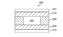
特許文献1には、CPTを利用した原子発振器のガスセル構造について開示されている。上記でも説明したとおり、原子のエネルギ遷移を利用する際に、原子をガス状態に保つ必要があるため、原子を気密封入したガスセルを一定の温度に保って動作させている。図6にはガスセル200を一定の温度に保持するために、キャビティ240の周囲にレイヤ210、220、230を配して、レイヤ210と220を挟むようにヒータ215により加熱してキャビティ240の温度を一定に保持している。
Patent Document 1 discloses a gas cell structure of an atomic oscillator using CPT. As described above, since it is necessary to keep atoms in a gas state when using energy transition of atoms, the gas cell in which atoms are hermetically sealed is kept operating at a constant temperature. In FIG. 6, in order to maintain the
しかし、特許文献1に開示されている従来の構成では、ガスセルを加熱するために、ヒータ215が必要となり、ガスセル全体が大きくなるといった問題と、ヒータ215に近い部分が過大に加熱されてしまうといった問題およびヒータによる光の吸収損失が生じるといった問題がある。
本発明は、かかる課題に鑑み、ガスセルを構成する基板上に発熱する素子を配置して基板自体を加熱することにより、部品点数を削減してガスセルを小型化すると共に、ガスセルの温度分布を均一にすることができ、且つ光吸収特性の劣化を改善した原子発振器の光学系を提供することを目的とする。
However, in the conventional configuration disclosed in Patent Document 1, the
In view of such problems, the present invention arranges a heat generating element on a substrate constituting the gas cell and heats the substrate itself, thereby reducing the number of parts and reducing the size of the gas cell and making the temperature distribution of the gas cell uniform. It is an object of the present invention to provide an optical system for an atomic oscillator that can improve the deterioration of light absorption characteristics.
本発明は、上述の課題の少なくとも一部を解決するためになされたものであり、以下の形態又は適用例として実現することが可能である。 SUMMARY An advantage of some aspects of the invention is to solve at least a part of the problems described above, and the invention can be implemented as the following forms or application examples.
[適用例1]
本発明はかかる課題を解決するために、波長が異なるコヒーレント光としての2種類の共鳴光を入射したときの量子干渉効果による光吸収特性を利用して発振周波数を制御する原子発振器の光学系であって、前記共鳴光を出射するコヒーレント光源と、前記コヒーレント光源の出射側に配置されガス状の金属原子を封入すると共に、該金属原子ガス中に共鳴光を通過させるガスセルと、前記ガスセルを通過した光を検出する光検出手段と、を備え、前記ガスセルは、前記金属原子を封入するために厚み方向に貫通した開口部を有するシリコン基板と、前記開口部の両端を夫々封止する透明部材と、を有し、前記シリコン基板に該シリコン基板を加熱する発熱素子を配置したことを特徴とする。
[Application Example 1]
In order to solve such a problem, the present invention is an optical system of an atomic oscillator that controls an oscillation frequency by utilizing a light absorption characteristic due to a quantum interference effect when two types of resonant light as coherent lights having different wavelengths are incident. A coherent light source that emits the resonance light, a gas cell that is disposed on the emission side of the coherent light source, encloses gaseous metal atoms, and passes the resonance light into the metal atom gas, and passes through the gas cell. A light detection means for detecting the light, and the gas cell includes a silicon substrate having an opening penetrating in the thickness direction to enclose the metal atoms, and a transparent member for sealing both ends of the opening. And a heating element for heating the silicon substrate is disposed on the silicon substrate.
本発明の原子発振器は、レーザ光などのコヒーレント光の量子干渉効果を利用したものである。この方式は、2つの基底準位が共鳴光を受けて、共通の励起準位と共鳴結合している3準位系(例えばΛ型準位系)において、同時に照射される2つの共鳴光の周波数が正確に基底準位1と基底準位2のエネルギ差に一致すると、3準位系は2つの基底準位の重ね合わせの状態になり、励起準位3への励起が停止する。CPTはこの原理を利用して、2つの共鳴光の一方或いは両方の波長を変化させたときに、ガスセルでの光吸収が停止する状態を検出して利用するものである。そして、本発明の光学系は、コヒーレント光源から出射した共鳴光はガスセルを通過し、ガスセルから出射した光は光検出手段により検出される。ここで、従来のルビジウム、セシウム等のアルカリ金属を用いた原子発振器は、原子のエネルギ遷移を利用する際に、原子をガス状態に保つ必要があるため、原子を気密封入したガスセルを一定の温度に保って動作させている。そのために、ガスセルを一定の温度に保持するために、キャビティの周囲にレイヤを配して、レイヤを挟むようにヒータにより加熱してキャビティの温度を一定に保持している。その結果、ガスセルを加熱するために、ヒータが必要となり、ガスセル全体が大きくなるといった問題と、ヒータに近い部分が過大に加熱されてしまうといった問題、および光吸収特性の劣化といった問題がある。そこで本発明では、ガスセルを構成するシリコン基板に発熱する素子を配置してシリコン基板自体を加熱することにより、部品点数を削減してガスセルを小型化すると共に、ガスセルの温度分布を均一にすることができる。
The atomic oscillator of the present invention utilizes the quantum interference effect of coherent light such as laser light. In this method, two ground levels of two resonant lights irradiated simultaneously in a three-level system (for example, a Λ-type level system) in which two ground levels receive resonant light and are resonantly coupled with a common excitation level. When the frequency exactly matches the energy difference between the ground level 1 and the ground level 2, the three-level system becomes a superposition state of the two ground levels, and the excitation to the
[適用例2]
また、前記シリコン基板に該シリコン基板の温度を検出する温度検出用素子を更に配置したことを特徴とする。
[Application Example 2]
Further, a temperature detecting element for detecting the temperature of the silicon substrate is further arranged on the silicon substrate.
シリコン基板上の温度を一定の値に保持するには、シリコン基板上の温度を検出しなければならない。そこで本発明では、シリコン基板に温度検出用素子を更に配置する。これにより、温度情報をフィードバックしてシリコン基板の温度を一定に制御することができる。 In order to maintain the temperature on the silicon substrate at a constant value, the temperature on the silicon substrate must be detected. Therefore, in the present invention, a temperature detecting element is further arranged on the silicon substrate. Thereby, the temperature information can be fed back to control the temperature of the silicon substrate to be constant.
[適用例3]
また、前記温度検出用素子による温度情報に基づいて、前記発熱素子の動作状態を制御する温度制御回路を前記シリコン基板の外部に備えたことを特徴とする。
[Application Example 3]
In addition, a temperature control circuit for controlling an operating state of the heat generating element based on temperature information from the temperature detecting element is provided outside the silicon substrate.
温度検出用素子からの温度情報は、シリコン基板の温度変化に追従して変化する。従って、温度と温度情報との関係が予めわかっていれば、温度情報からシリコン基板の温度を判断することができる。そこで本発明では、上限の温度に対する温度情報を受信すると、発熱素子を不動作として加熱を停止し、下限の温度に対する温度情報を受信すると、発熱素子を動作させて加熱を開始する温度制御回路、或いは連続動作により温度を一定に保つ温度制御回路等をシリコン基板の外部に備える。これにより、温度制御回路が基板温度の影響を受けずに、且つ制御方法をフレキシブルに変更することができる。 The temperature information from the temperature detecting element changes following the temperature change of the silicon substrate. Therefore, if the relationship between temperature and temperature information is known in advance, the temperature of the silicon substrate can be determined from the temperature information. Therefore, in the present invention, when temperature information with respect to the upper limit temperature is received, the heating element is deactivated and heating is stopped, and when temperature information with respect to the lower limit temperature is received, a temperature control circuit that operates the heating element to start heating, Alternatively, a temperature control circuit for keeping the temperature constant by continuous operation is provided outside the silicon substrate. Thereby, the temperature control circuit is not affected by the substrate temperature, and the control method can be changed flexibly.
[適用例4]
また、前記温度制御回路を前記発熱素子及び前記温度検出用素子と共に前記シリコン基板に配置したことを特徴とする。
[Application Example 4]
Further, the temperature control circuit is arranged on the silicon substrate together with the heating element and the temperature detecting element.
シリコン基板には、発熱素子と温度検出用素子が配置されているので、併せてこれらを制御する温度制御回路もシリコン基板に配置すれば、外部からは電源だけを供給すればよくなる。これにより、光学系全体を小型化することができる。 Since the heat generating element and the temperature detecting element are arranged on the silicon substrate, if a temperature control circuit for controlling them is also arranged on the silicon substrate, only the power source needs to be supplied from the outside. Thereby, the whole optical system can be reduced in size.
[適用例5]
また、前記シリコン基板面に均一な分布となるように複数の前記発熱素子を分散配置したことを特徴とする。
[Application Example 5]
In addition, a plurality of the heating elements are dispersedly arranged so as to have a uniform distribution on the surface of the silicon substrate.
シリコン基板は一定の面積を有するため、基板全体を加熱するためには、1箇所で加熱するより均一に分散配置した方が短い時間で一定の温度に達する。また、均一に分散配置することにより、温度勾配をなくすことができる。 Since the silicon substrate has a certain area, in order to heat the entire substrate, the uniform temperature distribution can reach a certain temperature in a shorter time than the heating at one place. Further, the temperature gradient can be eliminated by uniformly disposing the layers.
[適用例6]
また、複数の前記発熱素子を前記シリコン基板の外周に沿った位置に配置したことを特徴とする。
[Application Example 6]
The plurality of heating elements are arranged at positions along the outer periphery of the silicon substrate.
基板の外周は外気に曝されるため、温度の低下が大きい。そこで本発明では、基板の外周に沿った位置に発熱素子を配置する。これにより、外気による温度低下を最小限にすることができる。 Since the outer periphery of the substrate is exposed to the outside air, the temperature is greatly reduced. Therefore, in the present invention, the heating element is arranged at a position along the outer periphery of the substrate. Thereby, the temperature fall by external air can be minimized.
[適用例7]
また、前記シリコン基板の外周に沿った位置にはパワーの大きな発熱素子を配置し、前記パワーの大きな発熱素子群の内側にはパワーの小さな発熱素子を配置したことを特徴とする。
[Application Example 7]
Further, a heat generating element having a large power is disposed at a position along the outer periphery of the silicon substrate, and a heat generating element having a small power is disposed inside the heat generating element group having a large power.
基板の外周は温度低下が大きく、内周にいくほど小さくなる。そこで本発明では、基板の外周に沿った位置にはパワーの大きな発熱素子を配置し、内周にはパワーの小さな発熱素子を配置する。これにより、加熱速度を高めると共に、温度勾配を低減することができる。 The outer periphery of the substrate has a large temperature drop, and becomes smaller as it goes to the inner periphery. Therefore, in the present invention, a heating element having a large power is disposed at a position along the outer periphery of the substrate, and a heating element having a small power is disposed on the inner periphery. Thereby, while increasing a heating rate, a temperature gradient can be reduced.
[適用例8]
また、前記コヒーレント光は、レーザ光であることを特徴とする。
[Application Example 8]
The coherent light is laser light.
普通の光は、いろいろな波長が混ざり位相がランダムな光である。これに対してレーザ光は波長の単色性が良く、位相の揃った光である。このような光の波長や位相の安定性の尺度としてコヒーレンスが定義されている。コヒーレンスが良い、すなわち波長や位相が安定な光は量子干渉効果を起こすことができる。その点ではレーザ光は最適である。 Ordinary light is light in which various wavelengths are mixed and the phase is random. On the other hand, laser light has good monochromaticity in wavelength and is light with a uniform phase. Coherence is defined as a measure of the stability of the wavelength and phase of light. Light with good coherence, that is, with stable wavelength and phase, can cause a quantum interference effect. In that respect, laser light is optimal.
[適用例9]
また、前記ガス状の金属原子は、ルビジウム、又はセシウムであることを特徴とする。
[Application Example 9]
The gaseous metal atom is rubidium or cesium.
セシウム原子を使えば、精度の高い原子発振器を実現できる。また、ルビジウム原子は手軽に広く普及している。よって、原子発振器の要求性能とコストを考慮して、いずれかの金属原子を選ぶことができる。 If cesium atoms are used, a highly accurate atomic oscillator can be realized. In addition, rubidium atoms are widely spread easily. Therefore, any metal atom can be selected in consideration of the required performance and cost of the atomic oscillator.
[適用例10]
また、上記構成による光学系を原子発振器に備えたことを特徴とする。
[Application Example 10]
Further, the optical system having the above configuration is provided in an atomic oscillator.
部品点数を削減してガスセルを小型化すると共に、ガスセルの温度分布を均一にすることができ、且つ光吸収特性の劣化を改善できるので、小型でしかもガスセルの温度安定度が高い高性能な原子発振器を提供することができる。 The gas cell can be made smaller by reducing the number of parts, the temperature distribution of the gas cell can be made uniform, and the deterioration of light absorption characteristics can be improved. An oscillator can be provided.
以下、本発明を図に示した実施形態を用いて詳細に説明する。但し、この実施形態に記載される構成要素、種類、組み合わせ、形状、その相対配置などは特定的な記載がない限り、この発明の範囲をそれのみに限定する主旨ではなく単なる説明例に過ぎない。
図1は本発明の実施形態に係る原子発振器の光学系の要部構成図である。この光学系1は、波長が異なるコヒーレント光としての2種類の共鳴光を入射したときの量子干渉効果による光吸収特性を利用して発振周波数を制御する原子発振器50の光学系1であって、共鳴光2aを出射するコヒーレント光源2と、コヒーレント光源2の出射側に配置されガス状の金属原子を封入すると共に、金属原子ガス中に共鳴光2aを通過させるガスセル3と、ガスセル3を通過した光3aを検出する光検出器(光検出手段)4と、を備えている。また、原子発振器50は光検出器4の出力信号により、発振周波数を制御する周波数制御回路8を更に備えて構成されている。また、本実施形態では、ガスセル3に配置された温度センサ(温度検出用素子)の情報6に基づいてガスセル3に配置した発熱素子の動作を制御する温度制御回路5を備えている(詳細は後述する)。尚、本発明の主旨は、原子発振器を構成する光学系の構成にあるので、原子発振器の周波数制御についての詳細な説明は省略する。
Hereinafter, the present invention will be described in detail with reference to embodiments shown in the drawings. However, the components, types, combinations, shapes, relative arrangements, and the like described in this embodiment are merely illustrative examples and not intended to limit the scope of the present invention only unless otherwise specified. .
FIG. 1 is a configuration diagram of a main part of an optical system of an atomic oscillator according to an embodiment of the present invention. This optical system 1 is an optical system 1 of an
即ち、本発明の原子発振器50は、レーザ光などのコヒーレント光の量子干渉効果を利用したものである。この方式は、2つの基底準位が共鳴光を受けて、共通の励起準位と共鳴結合している3準位系(例えばΛ型準位系)において、同時に照射される2つの共鳴光の周波数が正確に基底準位1と基底準位2のエネルギ差に一致すると、3準位系は2つの基底準位の重ね合わせの状態になり、励起準位3への励起が停止する。CPTはこの原理を利用して、2つの共鳴光の一方或いは両方の波長を変化させたときに、ガスセルでの光吸収が停止する状態を検出して利用するものである。そして、本発明の光学系1は、コヒーレント光源2から出射した共鳴光2aはガスセル3を通過し、ガスセル3から出射した光3aは光検出器4により検出される。ここで、従来のルビジウム、セシウム等のアルカリ金属を用いた原子発振器は、原子のエネルギ遷移を利用する際に、原子をガス状態に保つ必要があるため、原子を気密封入したガスセルを一定の温度に保って動作させている。そのために、ガスセルを一定の温度に保持するために、キャビティの周囲にレイヤを配して、レイヤを挟むようにヒータにより加熱してキャビティの温度を一定に保持している。その結果、ガスセルを加熱するために、ヒータが必要となり、ガスセル全体が大きくなるといった問題と、ヒータに近い部分が過大に加熱されてしまうといった問題、および光吸収特性の劣化といった問題がある。そこで本実施形態では、ガスセル3を構成するシリコン基板上に発熱する発熱素子を配置して基板自体を加熱することにより、部品点数を削減してガスセル3を小型化すると共に、ガスセル3の温度分布を均一にすることができ、且つ光吸収特性の劣化を改善できる。
That is, the
また、コヒーレント光は、レーザ光が使用される。即ち、普通の光(ランプ光源等)は、いろいろな波長が混ざり位相がランダムな光である。これに対してレーザ光は波長の単色性が良く、位相の揃った光である。このような光の波長や位相の安定性の尺度としてコヒーレンスが定義されている。コヒーレンスが良い、すなわち波長や位相が安定な光は量子干渉効果を起こすことができる。その点ではレーザ光は最適である。
また、ガス状の金属原子は、ルビジウム、又はセシウムが使用される。セシウム原子を使えば、精度の高い原子発振器を実現できる。また、ルビジウム原子は手軽に広く普及している。よって、原子発振器の要求性能とコストを考慮して、いずれかの金属原子を選ぶことができる。
また、上記構成による光学系1を原子発振器に備えることにより、部品点数を削減してガスセル3を小型化すると共に、ガスセルの温度分布を均一にすることができ、且つ光吸収特性の劣化を改善できるので、小型でしかもガスセル3の温度安定度が高い高性能な原子発振器を提供することができる。
Further, laser light is used as the coherent light. In other words, ordinary light (lamp light source or the like) is light in which various wavelengths are mixed and the phase is random. On the other hand, laser light has good monochromaticity in wavelength and is light with a uniform phase. Coherence is defined as a measure of the stability of the wavelength and phase of light. Light with good coherence, that is, with stable wavelength and phase, can cause a quantum interference effect. In that respect, laser light is optimal.
As the gaseous metal atom, rubidium or cesium is used. If cesium atoms are used, a highly accurate atomic oscillator can be realized. In addition, rubidium atoms are widely spread easily. Therefore, any metal atom can be selected in consideration of the required performance and cost of the atomic oscillator.
In addition, by providing the optical system 1 with the above configuration in the atomic oscillator, the number of components can be reduced, the
図2はCPT方式による原子の3準位系を説明する一例である。原子発振器に用いられるルビジウムやセシウムの基底準位は、核スピン−電子スピン相互作用による超微細構造により2種類の基底準位に分かれている。これらの基底準位の原子は光を吸収して、よりエネルギーの高い準位へ励起する。また、図2の様に2つの基底準位が光を受けて、共通の励起準位と共鳴結合している状態を2光子共鳴と言う。図2において、基底準位1(23)と基底準位2(24)は準位のエネルギが若干異なるため、共鳴光もそれぞれ共鳴光1(20)と共鳴光2(22)と波長が若干異なる。同時に照射される共鳴光1(20)と共鳴光2(22)の周波数差(波長の差)が正確に基底準位1(23)と基底準位2(24)のエネルギ差に一致すると、図2の系は2つの基底準位の重ね合わせ状態になり、励起準位21への励起が停止する。CPTはこの原理を利用して、共鳴光1(20)と共鳴光2(22)のどちらかまたは両方の波長を変化させたときに、ガスセル3での光吸収(つまり励起準位21への転換)が停止する状態を検出、利用する方式である。尚、この光吸収が停止する状態でガスセル3を通過する光3aをEIT信号と呼ぶ。
FIG. 2 is an example for explaining a three-level system of atoms by the CPT method. The rubidium and cesium ground levels used in the atomic oscillator are divided into two kinds of ground levels by the hyperfine structure due to the nuclear spin-electron spin interaction. These ground level atoms absorb light and excite to higher energy levels. A state in which two ground levels receive light and are resonantly coupled to a common excitation level as shown in FIG. 2 is called two-photon resonance. In FIG. 2, since the ground level 1 (23) and the ground level 2 (24) have slightly different levels of energy, the resonant light also has a wavelength slightly different from that of the resonant light 1 (20) and the resonant light 2 (22), respectively. Different. When the frequency difference (wavelength difference) between the resonant light 1 (20) and the resonant light 2 (22) irradiated at the same time exactly matches the energy difference between the ground level 1 (23) and the ground level 2 (24), The system shown in FIG. 2 enters a superposition state of two ground levels, and excitation to the
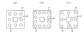
図3(a)は本発明の第1の実施形態に係るガスセルの構成を模式化した図である。図3(b)はシリコン基板上に配置した発熱素子を示す図である。このガスセル3は、少なくとも金属原子を封入するために厚み方向に貫通した開口部13を有するシリコン基板11と、開口部13を封止するガラス(透明部材)10、12と、を有し、図3(b)のようにシリコン基板11に、このシリコン基板11を加熱する発熱素子14、15、16を配置した。尚、図3(b)では、発熱素子としてバイポーラトランジスタ14、MOSトランジスタ15、抵抗16が示されているが、これらの何れか1種類だけで構成しても良く、或いは混在させても構わない。また、シリコン基板11は均一に加熱されることが重要なため、発熱素子はシリコン基板11上の一部に偏ることなく均一な分布となるように配置されるのが好ましい。
FIG. 3A is a diagram schematically showing the configuration of the gas cell according to the first embodiment of the present invention. FIG. 3B is a view showing a heating element arranged on the silicon substrate. The
また、シリコン基板11に、このシリコン基板11の温度を検出する温度センサを更に配置する。即ち、シリコン基板11の温度を一定の値に保持するには、シリコン基板11の温度を検出しなければならない。そこで本実施形態では、シリコン基板11に温度センサを更に配置する。これにより、温度情報をフィードバックして基板の温度を一定に制御することができる。温度センサは例えば抵抗値の変化を検出したり、サーミスタを配置してもよい。
また、温度サンサによる温度情報に基づいて、発熱素子の動作を制御する温度制御回路をシリコン基板11の外部に備える。即ち、温度センサからの温度情報は、シリコン基板11の温度変化に追従して変化する。従って、温度と温度情報との関係が予めわかっていれば、温度情報からシリコン基板11の温度を判断することができる。そこで本実施形態では、上限の温度に対する温度情報を受信すると、発熱素子を不動作として加熱を停止し、下限の温度に対する温度情報を受信すると、発熱素子を動作させて加熱を開始する温度制御回路、或いは連続動作により温度を一定に保つ温度制御回路等をシリコン基板11の外部に備える。これにより、温度制御回路が基板温度の影響を受けずに、且つ制御方法をフレキシブルに変更することができる。尚、温度制御回路は、発熱素子を動作させたり不動作とする制御方法の他に、発熱素子に流す電流値をアナログ的に変化させるように制御しても構わない。また、パルス幅を変調して電流をデジタル的に制御しても構わない。
Further, a temperature sensor for detecting the temperature of the
In addition, a temperature control circuit for controlling the operation of the heating element is provided outside the
また、温度制御回路をシリコン基板11に発熱素子及び温度センサと共に配置する。即ち、シリコン基板11には、発熱素子と温度センサが配置されているので、併せてこれらを制御する温度制御回路も基板に配置すれば、外部からは電源だけを供給すればよくなる。これにより、光学系全体を小型化することができる。
以上の説明では基板をシリコンとして説明したが、基板をガラスにより構成しても良い。即ち、基板をガラスにより構成し、ガラス上に回路を形成することも可能である。これにより、回路形成プロセスの選択幅を拡げることができる。
In addition, the temperature control circuit is arranged on the
In the above description, the substrate is described as silicon, but the substrate may be made of glass. That is, the substrate can be made of glass and a circuit can be formed on the glass. Thereby, the selection range of a circuit formation process can be expanded.
図4はシリコン基板上に配置された発熱素子のレイアウトを示す図である。図4(a)は、発熱素子17をシリコン基板11の一部に偏ることなく均一な分布となるように配置した図である。この場合、発熱素子17の種類を同一とし、シリコン基板11と開口部13の略中間に配置する。図4(b)はシリコン基板11の外周に沿った位置に発熱素子17を寄せて配置した図である。シリコン基板11は外側が外気に曝されるため、温度分布としては一番温度が低くなる。そこで、発熱素子17をシリコン基板11の外周に沿った位置に寄せて配置して、温度低下を低減するものである。図4(c)はシリコン基板11の外周に沿った位置にパワーの大きい発熱素子17を配し、内側にパワーの小さい発熱素子18を配置する。これにより、温度低下の大きい外側は加熱温度を高くし、温度低下の少ない内側は加熱温度を低くして、全体的に温度を効率よく均一にすることができる。
FIG. 4 is a view showing a layout of the heat generating elements arranged on the silicon substrate. FIG. 4A is a diagram in which the
このように、発熱素子はシリコン基板11上に自由に配置できるので、ガスセルの大きさや、使用環境に応じて最適な発熱素子を配置することができる。尚、この配置は一例であり、他の配置にしても構わない。
即ち、シリコン基板11は一定の面積を有するため、シリコン基板全体を加熱するためには、1箇所で加熱するよりも均一に分布するように分散配置した方が短い時間で一定の温度に達する。また、均一に配置することにより、温度勾配をなくすことができる。また、シリコン基板11の外周は外気に曝されるため、温度の低下が大きい。そこで本実施形態では、シリコン基板11の外周に沿った位置に発熱素子17を配置する。これにより、外気による温度低下を最小限にすることができる。また、シリコン基板11の外周は温度低下が大きく、内周に行くほど小さくなる。そこで本実施形態では、シリコン基板11の外周に沿った位置にはパワーの大きな発熱素子17を配置し、内周にはパワーの小さな発熱素子18を配置する。これにより、加熱速度を高めると共に、温度勾配を低減することができる。
As described above, since the heating element can be freely arranged on the
In other words, since the
図5はシリコン基板上に配置された温度センサのレイアウトを示す図である。図5(a)は温度センサ19をシリコン基板11の4箇所に配置した図である。シリコン基板の温度は全体が一定温度に達するまでには、所定の時間が必要となる。そこで温度センサ19をシリコン基板11の4箇所に均等に配置し、各温度センサからの温度情報に基づいて、その温度センサの周辺にある発熱素子を制御する。これにより、無駄な加熱を削減することができ、効率よくシリコン基板を加熱することができる。図5(b)は温度センサ19を開口部13の近傍に配置した図である。開口部13にはガス状の金属原子が封入されている。そして金属原子をガス状態に保つ必要があるため、金属原子を気密封入したガスセルを一定の温度に保って動作させている。そのため、開口部13の温度が所定の温度になることが重要である。そこで温度センサ19を開口部13の近傍に配置する。これにより、金属原子を効率よくガス状態にすることができる。
FIG. 5 is a view showing a layout of the temperature sensor arranged on the silicon substrate. FIG. 5A is a diagram in which the
1 光学系、2 コヒーレント光源、2a 共鳴光、3 ガスセル、4 光検出器、5 温度制御回路、6 温度情報、7 制御信号、8 周波数制御回路、10、12 ガラス、11 シリコン基板、13 開口部、14、15、16 発熱素子、50 原子発振器
DESCRIPTION OF SYMBOLS 1 Optical system, 2 Coherent light source, 2a Resonant light, 3 Gas cell, 4 Photo detector, 5 Temperature control circuit, 6 Temperature information, 7 Control signal, 8
Claims (10)
前記共鳴光を出射するコヒーレント光源と、
前記コヒーレント光源の出射側に配置されガス状の金属原子を封入すると共に、該金属原子ガス中に共鳴光を通過させるガスセルと、
前記ガスセルを通過した光を検出する光検出手段と、
を備え、
前記ガスセルは、前記金属原子を封入するために厚み方向に貫通した開口部を有するシリコン基板と、前記開口部の両端を夫々封止する透明部材と、を有し、
前記シリコン基板に該シリコン基板を加熱する発熱素子を配置したことを特徴とする原子発振器の光学系。 An optical system of an atomic oscillator that controls an oscillation frequency by utilizing a light absorption characteristic due to a quantum interference effect when two types of resonance light as coherent light having different wavelengths are incident,
A coherent light source that emits the resonant light;
A gas cell that is disposed on the emission side of the coherent light source and encloses gaseous metal atoms, and allows resonance light to pass through the metal atom gas; and
A light detection means for detecting light that has passed through the gas cell;
With
The gas cell includes a silicon substrate having an opening that penetrates in the thickness direction to enclose the metal atoms, and a transparent member that seals both ends of the opening,
An optical system of an atomic oscillator, wherein a heating element for heating the silicon substrate is disposed on the silicon substrate.
Priority Applications (1)
| Application Number | Priority Date | Filing Date | Title |
|---|---|---|---|
| JP2008012284A JP2009176852A (en) | 2008-01-23 | 2008-01-23 | Optical system and atomic oscillator |
Applications Claiming Priority (1)
| Application Number | Priority Date | Filing Date | Title |
|---|---|---|---|
| JP2008012284A JP2009176852A (en) | 2008-01-23 | 2008-01-23 | Optical system and atomic oscillator |
Publications (2)
| Publication Number | Publication Date |
|---|---|
| JP2009176852A true JP2009176852A (en) | 2009-08-06 |
| JP2009176852A5 JP2009176852A5 (en) | 2011-03-03 |
Family
ID=41031661
Family Applications (1)
| Application Number | Title | Priority Date | Filing Date |
|---|---|---|---|
| JP2008012284A Withdrawn JP2009176852A (en) | 2008-01-23 | 2008-01-23 | Optical system and atomic oscillator |
Country Status (1)
| Country | Link |
|---|---|
| JP (1) | JP2009176852A (en) |
Cited By (5)
| Publication number | Priority date | Publication date | Assignee | Title |
|---|---|---|---|---|
| US8970309B2 (en) | 2011-07-13 | 2015-03-03 | Ricoh Company, Ltd. | Atomic oscillator and method for fabricating atomic oscillator |
| WO2017018846A1 (en) * | 2015-07-30 | 2017-02-02 | 한국과학기술원 | Vapor cell comprising electro-optic function for chip-scale atomic clock, and method for manufacturing sealed container for chip-scale instrument |
| KR20170014602A (en) * | 2015-07-30 | 2017-02-08 | 한국과학기술원 | Vapor cell with electro-optical function for chip-scale atomic clock |
| JP2018042079A (en) * | 2016-09-07 | 2018-03-15 | セイコーエプソン株式会社 | Atomic oscillator |
| JP2020113616A (en) * | 2019-01-10 | 2020-07-27 | 国立研究開発法人情報通信研究機構 | Quantum optical device |
Citations (2)
| Publication number | Priority date | Publication date | Assignee | Title |
|---|---|---|---|---|
| US20060022761A1 (en) * | 2004-07-16 | 2006-02-02 | Abeles Joseph H | Chip-scale atomic clock (CSAC) and method for making same |
| JP2007336136A (en) * | 2006-06-14 | 2007-12-27 | Epson Toyocom Corp | Atomic oscillator, method of controlling temperature thereof, passive atomic oscillator, and method of controlling temperature thereof |
-
2008
- 2008-01-23 JP JP2008012284A patent/JP2009176852A/en not_active Withdrawn
Patent Citations (2)
| Publication number | Priority date | Publication date | Assignee | Title |
|---|---|---|---|---|
| US20060022761A1 (en) * | 2004-07-16 | 2006-02-02 | Abeles Joseph H | Chip-scale atomic clock (CSAC) and method for making same |
| JP2007336136A (en) * | 2006-06-14 | 2007-12-27 | Epson Toyocom Corp | Atomic oscillator, method of controlling temperature thereof, passive atomic oscillator, and method of controlling temperature thereof |
Cited By (7)
| Publication number | Priority date | Publication date | Assignee | Title |
|---|---|---|---|---|
| US8970309B2 (en) | 2011-07-13 | 2015-03-03 | Ricoh Company, Ltd. | Atomic oscillator and method for fabricating atomic oscillator |
| WO2017018846A1 (en) * | 2015-07-30 | 2017-02-02 | 한국과학기술원 | Vapor cell comprising electro-optic function for chip-scale atomic clock, and method for manufacturing sealed container for chip-scale instrument |
| KR20170014602A (en) * | 2015-07-30 | 2017-02-08 | 한국과학기술원 | Vapor cell with electro-optical function for chip-scale atomic clock |
| KR101709557B1 (en) | 2015-07-30 | 2017-02-23 | 한국과학기술원 | Vapor cell with electro-optical function for chip-scale atomic clock |
| US10447286B2 (en) | 2015-07-30 | 2019-10-15 | Korea Advanced Institute Of Science And Technology | Vapor cell comprising electro-optic function for chip-scale atomic clock, and method for manufacturing sealed container for chip-scale instrument |
| JP2018042079A (en) * | 2016-09-07 | 2018-03-15 | セイコーエプソン株式会社 | Atomic oscillator |
| JP2020113616A (en) * | 2019-01-10 | 2020-07-27 | 国立研究開発法人情報通信研究機構 | Quantum optical device |
Similar Documents
| Publication | Publication Date | Title |
|---|---|---|
| US7999626B2 (en) | Physical section of atomic oscillator | |
| JP4720635B2 (en) | Atomic oscillator, passive atomic oscillator, temperature control method for atomic oscillator, and temperature control method for passive atomic oscillator | |
| US8593229B2 (en) | Atomic oscillator | |
| JP5724492B2 (en) | Atomic oscillator | |
| JP5910808B2 (en) | Optical module and atomic oscillator for an atomic oscillator | |
| JP2009176852A (en) | Optical system and atomic oscillator | |
| JP5874522B2 (en) | Oscillator and electronic device | |
| JP5217661B2 (en) | Atomic oscillator | |
| JP2009231688A (en) | Optical system and atomic oscillator | |
| US8803618B2 (en) | Optical module for atomic oscillator and atomic oscillator | |
| JP5724480B2 (en) | Atomic oscillator and method for manufacturing atomic oscillator | |
| JP4941249B2 (en) | Optical system and atomic oscillator | |
| US10756743B2 (en) | Atomic oscillator and electronic device | |
| US10707884B2 (en) | Atomic oscillator and electronic apparatus | |
| US8830005B2 (en) | Optical module for atomic oscillator and atomic oscillator | |
| JP6160021B2 (en) | Atomic oscillator | |
| JP2015228461A (en) | Atomic resonance transition device, atomic oscillator, electronic apparatus, and movable body | |
| JP2009141048A (en) | Optical system and atomic oscillator | |
| JP2009283810A (en) | Optical system, and atomic oscillator | |
| JP2010109411A (en) | Atomic oscillator | |
| JP6060568B2 (en) | Gas cell unit, atomic oscillator and electronic equipment | |
| JP2010003944A (en) | Atomic oscillator | |
| JP2009232335A (en) | Optical system and atomic oscillator | |
| Prazot et al. | The medium and long term stability of the NAC atomic clock | |
| JP2006210967A (en) | Rubidium atomic oscillator |
Legal Events
| Date | Code | Title | Description |
|---|---|---|---|
| A521 | Written amendment |
Free format text: JAPANESE INTERMEDIATE CODE: A523 Effective date: 20110119 |
|
| A621 | Written request for application examination |
Free format text: JAPANESE INTERMEDIATE CODE: A621 Effective date: 20110119 |
|
| A711 | Notification of change in applicant |
Effective date: 20110729 Free format text: JAPANESE INTERMEDIATE CODE: A712 |
|
| RD03 | Notification of appointment of power of attorney |
Free format text: JAPANESE INTERMEDIATE CODE: A7423 Effective date: 20110729 |
|
| A521 | Written amendment |
Effective date: 20110819 Free format text: JAPANESE INTERMEDIATE CODE: A523 |
|
| A131 | Notification of reasons for refusal |
Free format text: JAPANESE INTERMEDIATE CODE: A131 Effective date: 20130416 |
|
| A761 | Written withdrawal of application |
Free format text: JAPANESE INTERMEDIATE CODE: A761 Effective date: 20130515 |