JP2009171298A - Digital-to-analog converter - Google Patents
Digital-to-analog converter Download PDFInfo
- Publication number
- JP2009171298A JP2009171298A JP2008007957A JP2008007957A JP2009171298A JP 2009171298 A JP2009171298 A JP 2009171298A JP 2008007957 A JP2008007957 A JP 2008007957A JP 2008007957 A JP2008007957 A JP 2008007957A JP 2009171298 A JP2009171298 A JP 2009171298A
- Authority
- JP
- Japan
- Prior art keywords
- mos transistors
- converter
- circuit
- reference voltages
- mos transistor
- Prior art date
- Legal status (The legal status is an assumption and is not a legal conclusion. Google has not performed a legal analysis and makes no representation as to the accuracy of the status listed.)
- Withdrawn
Links
- 239000000470 constituent Substances 0.000 abstract description 4
- 101100112673 Rattus norvegicus Ccnd2 gene Proteins 0.000 description 10
- 239000004973 liquid crystal related substance Substances 0.000 description 10
- 229920005994 diacetyl cellulose Polymers 0.000 description 8
- 238000010586 diagram Methods 0.000 description 6
- 230000002542 deteriorative effect Effects 0.000 description 3
- 230000008878 coupling Effects 0.000 description 2
- 238000010168 coupling process Methods 0.000 description 2
- 238000005859 coupling reaction Methods 0.000 description 2
- 230000004048 modification Effects 0.000 description 2
- 238000012986 modification Methods 0.000 description 2
- 239000003990 capacitor Substances 0.000 description 1
- 230000007423 decrease Effects 0.000 description 1
- 230000000694 effects Effects 0.000 description 1
- 239000011159 matrix material Substances 0.000 description 1
- 239000004065 semiconductor Substances 0.000 description 1
- 239000010409 thin film Substances 0.000 description 1
Images


Classifications
-
- H—ELECTRICITY
- H03—ELECTRONIC CIRCUITRY
- H03M—CODING; DECODING; CODE CONVERSION IN GENERAL
- H03M1/00—Analogue/digital conversion; Digital/analogue conversion
- H03M1/66—Digital/analogue converters
- H03M1/68—Digital/analogue converters with conversions of different sensitivity, i.e. one conversion relating to the more significant digital bits and another conversion to the less significant bits
- H03M1/682—Digital/analogue converters with conversions of different sensitivity, i.e. one conversion relating to the more significant digital bits and another conversion to the less significant bits both converters being of the unary decoded type
-
- G—PHYSICS
- G09—EDUCATION; CRYPTOGRAPHY; DISPLAY; ADVERTISING; SEALS
- G09G—ARRANGEMENTS OR CIRCUITS FOR CONTROL OF INDICATING DEVICES USING STATIC MEANS TO PRESENT VARIABLE INFORMATION
- G09G3/00—Control arrangements or circuits, of interest only in connection with visual indicators other than cathode-ray tubes
- G09G3/20—Control arrangements or circuits, of interest only in connection with visual indicators other than cathode-ray tubes for presentation of an assembly of a number of characters, e.g. a page, by composing the assembly by combination of individual elements arranged in a matrix no fixed position being assigned to or needed to be assigned to the individual characters or partial characters
- G09G3/34—Control arrangements or circuits, of interest only in connection with visual indicators other than cathode-ray tubes for presentation of an assembly of a number of characters, e.g. a page, by composing the assembly by combination of individual elements arranged in a matrix no fixed position being assigned to or needed to be assigned to the individual characters or partial characters by control of light from an independent source
- G09G3/36—Control arrangements or circuits, of interest only in connection with visual indicators other than cathode-ray tubes for presentation of an assembly of a number of characters, e.g. a page, by composing the assembly by combination of individual elements arranged in a matrix no fixed position being assigned to or needed to be assigned to the individual characters or partial characters by control of light from an independent source using liquid crystals
- G09G3/3611—Control of matrices with row and column drivers
- G09G3/3685—Details of drivers for data electrodes
- G09G3/3688—Details of drivers for data electrodes suitable for active matrices only
-
- G—PHYSICS
- G09—EDUCATION; CRYPTOGRAPHY; DISPLAY; ADVERTISING; SEALS
- G09G—ARRANGEMENTS OR CIRCUITS FOR CONTROL OF INDICATING DEVICES USING STATIC MEANS TO PRESENT VARIABLE INFORMATION
- G09G3/00—Control arrangements or circuits, of interest only in connection with visual indicators other than cathode-ray tubes
- G09G3/20—Control arrangements or circuits, of interest only in connection with visual indicators other than cathode-ray tubes for presentation of an assembly of a number of characters, e.g. a page, by composing the assembly by combination of individual elements arranged in a matrix no fixed position being assigned to or needed to be assigned to the individual characters or partial characters
- G09G3/34—Control arrangements or circuits, of interest only in connection with visual indicators other than cathode-ray tubes for presentation of an assembly of a number of characters, e.g. a page, by composing the assembly by combination of individual elements arranged in a matrix no fixed position being assigned to or needed to be assigned to the individual characters or partial characters by control of light from an independent source
- G09G3/36—Control arrangements or circuits, of interest only in connection with visual indicators other than cathode-ray tubes for presentation of an assembly of a number of characters, e.g. a page, by composing the assembly by combination of individual elements arranged in a matrix no fixed position being assigned to or needed to be assigned to the individual characters or partial characters by control of light from an independent source using liquid crystals
- G09G3/3611—Control of matrices with row and column drivers
- G09G3/3696—Generation of voltages supplied to electrode drivers
-
- G—PHYSICS
- G09—EDUCATION; CRYPTOGRAPHY; DISPLAY; ADVERTISING; SEALS
- G09G—ARRANGEMENTS OR CIRCUITS FOR CONTROL OF INDICATING DEVICES USING STATIC MEANS TO PRESENT VARIABLE INFORMATION
- G09G2310/00—Command of the display device
- G09G2310/02—Addressing, scanning or driving the display screen or processing steps related thereto
- G09G2310/0264—Details of driving circuits
- G09G2310/027—Details of drivers for data electrodes, the drivers handling digital grey scale data, e.g. use of D/A converters
-
- H—ELECTRICITY
- H03—ELECTRONIC CIRCUITRY
- H03M—CODING; DECODING; CODE CONVERSION IN GENERAL
- H03M1/00—Analogue/digital conversion; Digital/analogue conversion
- H03M1/66—Digital/analogue converters
- H03M1/74—Simultaneous conversion
- H03M1/76—Simultaneous conversion using switching tree
-
- H—ELECTRICITY
- H03—ELECTRONIC CIRCUITRY
- H03M—CODING; DECODING; CODE CONVERSION IN GENERAL
- H03M1/00—Analogue/digital conversion; Digital/analogue conversion
- H03M1/66—Digital/analogue converters
- H03M1/74—Simultaneous conversion
- H03M1/76—Simultaneous conversion using switching tree
- H03M1/765—Simultaneous conversion using switching tree using a single level of switches which are controlled by unary decoded digital signals
Landscapes
- Engineering & Computer Science (AREA)
- Theoretical Computer Science (AREA)
- Chemical & Material Sciences (AREA)
- Crystallography & Structural Chemistry (AREA)
- Physics & Mathematics (AREA)
- Computer Hardware Design (AREA)
- General Physics & Mathematics (AREA)
- Analogue/Digital Conversion (AREA)
- Control Of Indicators Other Than Cathode Ray Tubes (AREA)
- Liquid Crystal Display Device Control (AREA)
- Liquid Crystal (AREA)
Abstract
Description
本発明は、デジタル・アナログコンバータ(digital-to-analog converter:DAC)に関し、特に液晶ディスプレイ等の画像表示装置に好適に用いられるDACに関するものである。 The present invention relates to a digital-to-analog converter (DAC), and more particularly to a DAC suitably used for an image display device such as a liquid crystal display.
従来の液晶ディスプレイ用DACの1つとして、基準電圧生成回路と、複数のスイッチ対を有する選択回路と、ボルテージフォロアとを持つDACが知られている。具体的には、当該DACが6ビットのデジタル信号を入力コードとして受け取る場合、基準電圧生成回路は、32個の抵抗素子を直列接続してなり、当該抵抗素子の各端子から互いに異なる33個の基準電圧を選択回路へ供給する。選択回路は、各々入力コードの対応ビットに従って2入力のうち一方を選択する37個のスイッチ対からなり、入力コードが奇数ならば33個の基準電圧のうち互いに隣接する2つの基準電圧を選択し、入力コードが偶数ならば33個の基準電圧のうちの1つの基準電圧を重複選択して、これらの電圧をボルテージフォロアへ供給する。ボルテージフォロアは、供給された2つの電圧の平均値をアナログ信号として出力する。つまり、入力コードが奇数の場合には、隣接する2つの基準電圧の中間電圧をボルテージフォロアで生成し、これを階調電圧とするのである(特許文献1参照)。 As one of conventional DACs for liquid crystal displays, a DAC having a reference voltage generation circuit, a selection circuit having a plurality of switch pairs, and a voltage follower is known. Specifically, when the DAC receives a 6-bit digital signal as an input code, the reference voltage generation circuit includes 32 resistance elements connected in series, and each of the resistance elements has 33 different terminals. A reference voltage is supplied to the selection circuit. The selection circuit is composed of 37 switch pairs for selecting one of the two inputs according to the corresponding bit of the input code. If the input code is an odd number, two adjacent reference voltages are selected from the 33 reference voltages. If the input code is an even number, one of the 33 reference voltages is selected redundantly, and these voltages are supplied to the voltage follower. The voltage follower outputs an average value of two supplied voltages as an analog signal. That is, when the input code is an odd number, an intermediate voltage between two adjacent reference voltages is generated by a voltage follower and used as a gradation voltage (see Patent Document 1).
このDACでは、入力ビット数(分解能)が6から8、10と増えるに従い、生成すべき基準電圧の数が33から129、513のように急激に増え、選択回路に必要なスイッチ対の数が37から135、521のように急激に増える。したがって、液晶ディスプレイの高精細化及び多階調化が進んでいる現状に鑑みて、DACのチップサイズを大きくせざるを得なくなってしまう。 In this DAC, as the number of input bits (resolution) increases from 6 to 8, 10, the number of reference voltages to be generated increases rapidly from 33 to 129, 513, and the number of switch pairs necessary for the selection circuit increases. It increases rapidly from 37 to 135, 521. Therefore, in view of the current situation in which the liquid crystal display is becoming higher in definition and multi-gradation, the chip size of the DAC must be increased.
そこで、互いに隣接する2つの基準電圧を選択し、MOS(metal-oxide-semiconductor)トランジスタのオン抵抗を利用して当該2基準電圧の差を分割することにより所望の中間階調電圧を得るようにしたDACが開発された(特許文献2参照)。
上記MOSトランジスタのオン抵抗を利用したDACを液晶ディスプレイに採用する場合、抵抗ストリングからなる基準電圧生成回路を多数のDACが共有することとなる。そのため、複数のDACが同じ2基準電圧の組を選択して分圧動作を実行する場合、基準電圧生成回路中の特定の抵抗素子に対して複数のDACのMOSトランジスタ(オン状態)がそれぞれ並列につながり、ここに電流の分流が生じるため、基準電圧生成回路にて生成した基準電圧そのものがずれてしまう。 When a DAC using the on-resistance of the MOS transistor is employed in a liquid crystal display, a large number of DACs share a reference voltage generation circuit composed of a resistor string. Therefore, when a plurality of DACs select the same set of two reference voltages and execute a voltage dividing operation, a plurality of DAC MOS transistors (ON state) are in parallel with a specific resistance element in the reference voltage generation circuit. As a result, current shunting occurs here, so that the reference voltage itself generated by the reference voltage generation circuit shifts.
この電圧ずれを抑えるには、分圧に利用されるMOSトランジスタ群の合成オン抵抗を大きくすればよい。例えばMOSトランジスタ数を増やす、各MOSトランジスタのゲート長を伸ばすなどである。しかし、合成オン抵抗を大きくするとDACのセトリング時間が長くなり、その結果所定の時間内に所望の階調電圧を出力できなくなってしまうという課題がある。 In order to suppress this voltage deviation, the combined on-resistance of the MOS transistor group used for voltage division may be increased. For example, the number of MOS transistors is increased, and the gate length of each MOS transistor is increased. However, when the combined on-resistance is increased, the settling time of the DAC becomes longer, and as a result, there is a problem that a desired gradation voltage cannot be output within a predetermined time.
本発明の目的は、同じセトリング時間と同じ分解能とを維持しつつDACの構成素子数を削減することにある。 An object of the present invention is to reduce the number of components of a DAC while maintaining the same settling time and the same resolution.
本発明では、分圧対象となる2基準電圧の大きさに応じてMOSトランジスタのオン抵抗が異なる点に着目した。具体的には、PチャネルMOSトランジスタの場合は電源電圧付近の電圧を分圧対象とするときにオン抵抗が小さくなり、NチャネルMOSトランジスタの場合は接地電圧付近の電圧を分圧対象とするときにオン抵抗が小さくなる。いずれの場合もゲート・ソース間電圧Vgsが大きくなるからである。 In the present invention, attention is paid to the fact that the on-resistance of the MOS transistor differs depending on the magnitude of the two reference voltages to be divided. Specifically, in the case of a P-channel MOS transistor, the on-resistance decreases when a voltage near the power supply voltage is to be divided, and in the case of an N-channel MOS transistor, the voltage near the ground voltage is to be divided. The on-resistance becomes smaller. This is because the gate-source voltage Vgs increases in any case.
よって、本発明によれば、オン抵抗が大きい階調ではMOSトランジスタ数を少なくし、オン抵抗が小さい階調ではMOSトランジスタ数を多くするように切り替えできる回路構成を採用する。こうすることにより、セトリング時間を悪化させずに、電圧ずれを抑えられる。 Therefore, according to the present invention, a circuit configuration is employed that can be switched so that the number of MOS transistors is reduced in a gradation with a large on-resistance and the number of MOS transistors is increased in a gradation with a small on-resistance. By doing so, voltage deviation can be suppressed without deteriorating the settling time.
具体的に説明すると、本発明は、互いに異なる複数の基準電圧を用いてN(Nは3以上の整数)ビットのデジタル信号をアナログ信号に変換するコンバータを、次のような選択分圧回路とモード選択回路と出力回路とで構成することとした。すなわち、選択分圧回路は、各々スイッチとして機能する複数のMOSトランジスタを有し、mを1以上の整数とし、2mから2m−1+1までの整数のうちのいずれかをMとするとき、前記デジタル信号のうちの上位(N−m)ビットに従って前記複数のMOSトランジスタのうち各々互いに同数のMOSトランジスタを通じて前記複数の基準電圧のうちの2つの基準電圧を選択し、かつ(M−1)個の中間電圧を得るように、前記選択された2つの基準電圧の差を、前記複数のMOSトランジスタのうち互いに直列接続されたM個のMOSトランジスタ群の各々の合成オン抵抗でM分割する。モード選択回路は、前記選択分圧回路の前記M個のMOSトランジスタ群の各々の合成オン抵抗の大きさを判別し、当該合成オン抵抗が大きい場合には第1モードを、当該合成オン抵抗が小さい場合には第2モードをそれぞれ選択し、かつ前記選択分圧回路の前記M個のMOSトランジスタ群の各々に含まれるMOSトランジスタの個数が前記第1モードよりも前記第2モードの方が多くなるように制御する。出力回路は、前記デジタル信号のうちの下位mビットに従って、前記選択された2つの基準電圧のうちの1つ又は前記(M−1)個の中間電圧のうちの1つを前記アナログ信号として選択的に出力する。 More specifically, the present invention relates to a converter for converting a digital signal of N (N is an integer of 3 or more) bits into an analog signal using a plurality of different reference voltages, and a selective voltage dividing circuit as follows. The mode selection circuit and the output circuit are used. That is, the selection voltage divider circuit has a plurality of MOS transistors which respectively function as a switch, when the integer of 1 or more to m, any of integers from 2 m to 2 m-1 +1 and M , Two reference voltages of the plurality of reference voltages are selected through the same number of MOS transistors among the plurality of MOS transistors according to upper (N−m) bits of the digital signal, and (M−1) ) Divide the difference between the two selected reference voltages by the combined on-resistance of each of the M MOS transistor groups connected in series among the plurality of MOS transistors so as to obtain intermediate voltages . The mode selection circuit determines the magnitude of the combined on-resistance of each of the M MOS transistor groups of the selection voltage dividing circuit, and when the combined on-resistance is large, the mode selection circuit selects the first mode. If it is smaller, the second mode is selected, and the number of MOS transistors included in each of the M MOS transistor groups of the selected voltage dividing circuit is larger in the second mode than in the first mode. Control to be. The output circuit selects one of the selected two reference voltages or one of the (M−1) intermediate voltages as the analog signal according to the lower m bits of the digital signal. To output automatically.
この場合の基準電圧生成回路は、互いに直列接続された2N−m個の抵抗素子を有し、当該抵抗素子の各端子から互いに異なる(2N−m+1)個の基準電圧を前記選択分圧回路へ供給する。 The reference voltage generation circuit in this case has 2 N−m resistance elements connected in series with each other, and (2 N−m +1) different reference voltages from each terminal of the resistance elements are selected. Supply to pressure circuit.
前記選択分圧回路が前記複数の基準電圧のうち互いに隣接する2つの基準電圧を選択するスイッチ回路を有する場合、当該スイッチ回路は、例えば、各々前記デジタル信号の上位(N−m)ビットのうちの対応ビットに従って2入力のうち一方を選択する複数のスイッチ対を有し、前記デジタル信号の上位(N−m)ビットのうち最下位ビットから数えてn番目のビットに対応するスイッチ対の数anは、
a1=2、an=an−1+2n−2(2≦n≦N−m)
にて与えられる。そして、前記複数のスイッチ対を構成するMOSトランジスタのうち各々(N−m)個のMOSトランジスタを通じて、前記互いに隣接する2つの基準電圧が選択される。この場合の前記選択分圧回路の前記M個のMOSトランジスタ群の各々は、例えば、互いに直列接続された(N−m+1)個以上のMOSトランジスタで構成される。前記M個のMOSトランジスタ群のうちの2つは、前記互いに直列接続された(N−m+1)個以上のMOSトランジスタの中に、前記互いに隣接する2つの基準電圧を選択するための(N−m)個のMOSトランジスタを含む。
When the selection voltage dividing circuit includes a switch circuit that selects two reference voltages adjacent to each other among the plurality of reference voltages, the switch circuit includes, for example, each of the upper (N−m) bits of the digital signal. The number of switch pairs corresponding to the nth bit counted from the least significant bit among the upper (N−m) bits of the digital signal, having a plurality of switch pairs for selecting one of the two inputs according to the corresponding bits a n is,
a 1 = 2 and a n = a n−1 +2 n−2 (2 ≦ n ≦ N−m)
Given in The two reference voltages adjacent to each other are selected through (N−m) MOS transistors among the MOS transistors constituting the plurality of switch pairs. In this case, each of the M MOS transistor groups of the selective voltage dividing circuit includes, for example, (N−m + 1) or more MOS transistors connected in series. Two of the M MOS transistor groups select (N−m + 1) for selecting two adjacent reference voltages among the (N−m + 1) or more MOS transistors connected in series. m) Includes MOS transistors.
また、前記選択分圧回路が前記複数の基準電圧のうち互いに隣接する2つの基準電圧を選択するスイッチ回路を有する場合、前記選択分圧回路は、Pを2以上かつ(N−m)以下の整数とするとき、前記デジタル信号の上位(N−m)ビットのうちの下位Pビットを、いずれか1個が有効にされる2P個の選択信号にデコードするデコード回路を更に有し、前記スイッチ回路は、例えば、各々前記2P個の選択信号のうちの対応する選択信号に従って2入力を2出力へ選択的に伝達する2P個のスイッチ対と、各々前記デジタル信号の上位(N−m−P)ビットのうちの対応ビットに従って2入力のうち一方を選択する複数の他のスイッチ対とで構成される。そして、前記全てのスイッチ対を構成するMOSトランジスタのうち各々(N−m−P+1)個のMOSトランジスタを通じて、前記互いに隣接する2つの基準電圧が選択される。この場合の前記選択分圧回路の前記M個のMOSトランジスタ群の各々は、例えば、互いに直列接続された(N−m−P+2)個以上のMOSトランジスタで構成される。前記M個のMOSトランジスタ群のうちの2つは、前記互いに直列接続された(N−m−P+2)個以上のMOSトランジスタの中に、前記互いに隣接する2つの基準電圧を選択するための(N−m−P+1)個のMOSトランジスタを含む。 In the case where the selection voltage dividing circuit has a switch circuit that selects two reference voltages adjacent to each other among the plurality of reference voltages, the selection voltage dividing circuit has P of 2 or more and (N−m) or less. When it is an integer, it further comprises a decoding circuit that decodes the lower P bits of the upper (N−m) bits of the digital signal into 2 P selection signals in which any one is enabled, the switch circuit may, for example, and each said 2 P number of the corresponding 2 selectively transmits two inputs to two outputs in accordance with selection signals for the P switch pairs of the selected signals, each said digital signal higher (N- m-P) and a plurality of other switch pairs that select one of the two inputs according to the corresponding bit. Then, the two adjacent reference voltages are selected through (N−m−P + 1) MOS transistors among the MOS transistors constituting all the switch pairs. In this case, each of the M MOS transistor groups of the selective voltage dividing circuit includes, for example, (N−m−P + 2) or more MOS transistors connected in series. Two of the M MOS transistor groups are for selecting two adjacent reference voltages among the (NmP + 2) or more MOS transistors connected in series with each other ( N−m−P + 1) MOS transistors are included.
本発明によれば、DACのセトリング時間を悪化させずに、同じ分解能を維持しつつDACの構成素子数を削減することができる。 According to the present invention, it is possible to reduce the number of components of a DAC while maintaining the same resolution without deteriorating the settling time of the DAC.
以下、本発明を実施するための最良の形態について、図面を用いながら説明する。 The best mode for carrying out the present invention will be described below with reference to the drawings.
図1は、本発明に係るDACを用いた画像表示装置の概略平面図である。図1に示した画像表示装置1は液晶ディスプレイであって、マトリックス状に配置された複数の画素を有する液晶ディスプレイパネル10と、複数のゲートドライバ20と、複数のソースドライバ25と、これらのゲートドライバ20及びソースドライバ25を制御するコントローラ30とを備えている。液晶ディスプレイパネル10の各画素は、TFT(thin film transistor)11と、そのドレインに接続された画素容量12とを持つ。同じ行に属する画素のTFT12のゲートは、共通のゲートドライバ20により駆動される。また、同じ列に属する画素のTFT12のソースは、共通のソースドライバ25により駆動される。全てのソースドライバ25は、コントローラ30から送られた画像の階調を表すデジタル信号に従って複数の画素を駆動する液晶駆動回路を構成し、デジタル信号を画素列毎のアナログ信号に変換するDACをそれぞれ内蔵している。つまり、画像表示装置1は、画素列と同数のDACを備えている。
FIG. 1 is a schematic plan view of an image display apparatus using a DAC according to the present invention. The
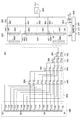
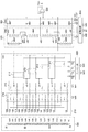
図2は、本発明に係るDACの構成例を示している。図2のDACは、bit5からbit0までの6ビットで表されるデジタル信号をアナログ信号Voutに変換するコンバータであって、基準電圧生成回路100と、第1のスイッチ回路(SW1)200と、第2のスイッチ回路(SW2)300と、第3のスイッチ回路(SW3)400と、ボルテージフォロア500と、論理回路600とで構成される。
FIG. 2 shows a configuration example of the DAC according to the present invention. The DAC in FIG. 2 is a converter that converts a digital signal represented by 6 bits from bit 5 to
基準電圧生成回路100は、互いに直列接続された16(=26−2)個の抵抗素子からなる抵抗分圧回路であって、当該抵抗素子の各端子から互いに異なる17個の基準電圧V0,V4,V8,…,V64を第1のスイッチ回路200へ供給する。
The reference
第1のスイッチ回路200は、17個の基準電圧V0〜V64のうち互いに隣接する2つの基準電圧(以下、低い方をVin1とし、高い方をVin2とする。)を選択する回路であって、6ビットデジタル信号のうちbit5からbit2までの上位4ビットを制御信号として受け取る。図中の201は、bit2によりオン/オフ制御される2個のスイッチ対である。202は、bit3によりオン/オフ制御される3(=2+22−2)個のスイッチ対である。203は、bit4によりオン/オフ制御される5(=3+23−2)個のスイッチ対である。204は、bit5によりオン/オフ制御される9(=5+24−2)個のスイッチ対である。以上のとおり、第1のスイッチ回路200は、各々bit5〜bit2のうちの対応ビットに従って2入力のうち一方を選択する19個の2入力・1出力スイッチ対で構成されている。各スイッチ対は、対応ビットが0ならば下側入力を、対応ビットが1ならば上側入力をそれぞれ選択する。
The
なお、第1のスイッチ回路200の各スイッチ対を構成する2個のスイッチは、それぞれNチャネルMOSトランジスタ又はPチャネルMOSトランジスタ又はこれらを結合してなるトランスファゲートである。ただし、以下の説明では各スイッチがPチャネルMOSトランジスタ(以下、単にMOSトランジスタという。)であるものとする。
Note that the two switches constituting each switch pair of the
例えば、bit5からbit2までの4ビットが“0000”ならば、最も低い基準電圧V0が4(=6−2)個のMOSトランジスタを通じて第2のスイッチ回路300に接続され、次に低い基準電圧V4が他の4(=6−2)個のMOSトランジスタを通じて第2のスイッチ回路300に接続される。この場合にはVin1=V0、Vin2=V4である。また、bit5からbit2までの4ビットが“0001”ならば、基準電圧V4が4個のMOSトランジスタを通じて第2のスイッチ回路300に接続され、次に高い基準電圧V8が他の4個のMOSトランジスタを通じて第2のスイッチ回路300に接続される。この場合にはVin1=V4、Vin2=V8である。bit5からbit2までの4ビットが“1111”ならば、基準電圧V60が4個のMOSトランジスタを通じて第2のスイッチ回路300に接続され、最も高い基準電圧V64が他の4個のMOSトランジスタを通じて第2のスイッチ回路300に接続される。この場合にはVin1=V60、Vin2=V64である。
For example, if 4 bits from bit 5 to
第2のスイッチ回路300及び第3のスイッチ回路400中に示した40個の丸印は、それぞれスイッチとして機能するNチャネルMOSトランジスタ又はPチャネルMOSトランジスタ又はこれらを結合してなるトランスファゲートである。ただし、以下の説明では各スイッチがPチャネルMOSトランジスタ(以下、単にMOSトランジスタという。)であるものとする。
Forty circles shown in the
第2のスイッチ回路300は、ノードn00とノードn01との間に接続された1個のMOSトランジスタM00と、ノードn01とノードn02との間に直列接続された5(=6−2+1)個のMOSトランジスタM01と、ノードn02とノードn03との間に直列接続された5(=6−2+1)個のMOSトランジスタM02と、ノードn03とノードn04との間に接続された1個のMOSトランジスタM03とを有する。また、第1のスイッチ回路200により選択された2つの基準電圧のうち低い方の電圧Vin1がノードn00に、高い方の電圧Vin2がノードn04にそれぞれ接続される。したがって、例えばbit5からbit2までの4ビットが“0000”であり、かつM00、M01、M02及びM03の全てがオンしているとき、基準電圧V0とノードn01との間、ノードn01とノードn02との間、ノードn02とノードn03との間、ノードn03と基準電圧V4との間に、それぞれオン状態の5個のMOSトランジスタからなるMOSトランジスタ群が介在することになり、これら4個の互いに直列接続されたMOSトランジスタ群の各々の合成オン抵抗によりV0とV4との差が4分割されて、3個の中間電圧が得られる。なお、基準電圧V0とノードn01との間のMOSトランジスタ群は第1のスイッチ回路200中の4個のMOSトランジスタを、ノードn03と基準電圧V4との間のMOSトランジスタ群は第1のスイッチ回路200中の他の4個のMOSトランジスタをそれぞれ含む。
The
しかも、上記4個のMOSトランジスタ群を構成する20個のMOSトランジスタのサイズが全て等しいとき、4個のMOSトランジスタ群の各々の合成オン抵抗が互いに等しくなるので、ノードn01に中間電圧V0+(V4−V0)/4が、ノードn02に中間電圧V0+(V4−V0)/2が、ノードn03に中間電圧V0+3(V4−V0)/4がそれぞれ得られる。なお、ノードn00の電圧を基準電圧V0にするためには、互いに直列接続された4個のMOSトランジスタ群に流れる電流を止めるように、M00、M01、M02、M03のうち少なくとも1つをオフにする。 Moreover, when the sizes of the 20 MOS transistors constituting the four MOS transistor groups are all equal, the combined on-resistances of the four MOS transistor groups are equal to each other, so that the intermediate voltage V0 + (V4) is applied to the node n01. -V0) / 4, intermediate voltage V0 + (V4-V0) / 2 is obtained at node n02, and intermediate voltage V0 + 3 (V4-V0) / 4 is obtained at node n03. In order to set the voltage at the node n00 to the reference voltage V0, at least one of M00, M01, M02, and M03 is turned off so as to stop the current flowing through the four MOS transistor groups connected in series with each other. To do.
第2のスイッチ回路300は更に、ノードn00とノードn00’との間に接続された6(=6−2+2)個のMOSトランジスタM00’と、ノードn00’とノードn01との間に接続された5(=6−2+1)個のMOSトランジスタM01’と、ノードn03とノードn03’との間に接続された5(=6−2+1)個のMOSトランジスタM02’と、ノードn03’とノードn04との間に接続された6(=6−2+2)個のMOSトランジスタM03’とを有する。したがって、例えばbit5からbit2までの4ビットが“1111”であり、かつM00’、M01’、M01、M02、M02’及びM03’の全てがオンし、かつM00及びM03がオフしているとき、基準電圧V60とノードn00’との間、ノードn00’とノードn02との間、ノードn02とノードn03’との間、ノードn03’と基準電圧V64との間に、それぞれオン状態の10個のMOSトランジスタからなるMOSトランジスタ群が介在することになり、これら4個の互いに直列接続されたMOSトランジスタ群の各々の合成オン抵抗によりV60とV64との差が4分割されて、3個の中間電圧が得られる。なお、基準電圧V60とノードn00’との間のMOSトランジスタ群は第1のスイッチ回路200中の4個のMOSトランジスタを、ノードn03’と基準電圧V64との間のMOSトランジスタ群は第1のスイッチ回路200中の他の4個のMOSトランジスタをそれぞれ含む。
The
しかも、上記4個のMOSトランジスタ群を構成する40個のMOSトランジスタのサイズが全て等しいとき、4個のMOSトランジスタ群の各々の合成オン抵抗が互いに等しくなるので、ノードn00’に中間電圧V60+(V64−V60)/4が、ノードn02に中間電圧V60+(V64−V60)/2が、ノードn03’に中間電圧V60+3(V64−V60)/4がそれぞれ得られる。なお、ノードn00の電圧を基準電圧V60にするためには、互いに直列接続された4個のMOSトランジスタ群に流れる電流を止めるように、M00、M01、M02、M03のうち少なくとも1つをオフ、かつM00’、M01’、M02’、M03’のうち少なくとも1つをオフにする。 Moreover, when the sizes of the 40 MOS transistors constituting the four MOS transistor groups are all equal, the combined on-resistances of the four MOS transistor groups are equal to each other, so that the intermediate voltage V60 + ( V64−V60) / 4, the intermediate voltage V60 + (V64−V60) / 2 is obtained at the node n02, and the intermediate voltage V60 + 3 (V64−V60) / 4 is obtained at the node n03 ′. In order to set the voltage of the node n00 to the reference voltage V60, at least one of M00, M01, M02, and M03 is turned off so as to stop the current flowing through the four MOS transistor groups connected in series with each other. And at least one of M00 ′, M01 ′, M02 ′, and M03 ′ is turned off.
第3のスイッチ回路400は、ノードn00とボルテージフォロア500の入力ノードとの間に接続された1個のMOSトランジスタM04と、ノードn01とボルテージフォロア500の入力ノードとの間に接続された1個のMOSトランジスタM05と、ノードn02とボルテージフォロア500の入力ノードとの間に接続された1個のMOSトランジスタM06と、ノードn03とボルテージフォロア500の入力ノードとの間に接続された1個のMOSトランジスタM07と、ノードn00’とボルテージフォロア500の入力ノードとの間に接続された1個のMOSトランジスタM04’と、ノードn03’とボルテージフォロア500の入力ノードとの間に接続された1個のMOSトランジスタM07’とで構成される。
The
論理回路600は、6ビットデジタル信号のうちbit1及びbit0からなる下位2ビット及び最上位ビット(bit5)に従って、第2及び第3のスイッチ回路300,400を制御するための信号S0〜S7,S0’〜S7’を生成する。この結果、第3のスイッチ回路400は、bit1、bit0及びbit5に従って、6個のノードn00,n01,n02,n03,n00’,n03’のうちいずれか1個のノードの電圧を選択して、これをボルテージフォロア500へ供給する。このようにして第3のスイッチ回路400により選択された電圧が、アナログ信号Voutとしてボルテージフォロア500から出力される。
The
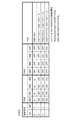
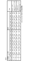
図3及び図4は図2中の第2及び第3のスイッチ回路300,400の動作を、図5は図2のDACの全体動作をそれぞれ示している。論理回路600により、bit5=0の場合には図3の第1モード動作が、bit5=1の場合には図4の第2モード動作がそれぞれ選択される。図3中のVn00,Vn01,Vn02,Vn03は、それぞれノードn00,n01,n02,n03の電圧であり、図4中のVn00’,Vn01’,Vn02’,Vn03’は、それぞれノードn00,n00’,n02,n03’の電圧である。第2のスイッチ回路300では、bit5が0のとき、例えばM01、M02及びM03を常にオンさせ、M00のみのオン/オフをbit1及びbit0からなる2ビットに応じた信号で制御すればよい。M05とM07とのサイズが等しいとき、Vn02をM06にて選択する代わりに、Vn01とVn03との差をM05とM07とのオン抵抗で2分割することにより、Vn01とVn03との中間電圧(Vn02に相当する。)を生成することも可能である。図5中のV1、V2、V3、V5、V6、V7等は、第1及び第2のスイッチ回路200,300により生成された中間電圧である。
3 and 4 show the operation of the second and
図6は、図2中の第2のスイッチ回路300の変形例を示している。ここで、MOSトランジスタのゲート幅Wとゲート長Lとの比を用いて、当該MOSトランジスタのサイズを「W/L」で表す。例えば、図2中のM01を構成する5個のMOSトランジスタの各々がサイズW/Lを有するとき、これら5個のMOSトランジスタの直列回路を1個のMOSトランジスタに置換することができる。ただし、後者のMOSトランジスタはサイズW/(5L)を有し、5個のMOSトランジスタの直列回路の合成オン抵抗と等しいオン抵抗を持つ。図2中のM02を構成する5個のMOSトランジスタ等についても同様の置換が可能である。
FIG. 6 shows a modification of the
以上のとおり、図2のDACによれば、第1及び第2のスイッチ回路200,300が前述の選択分圧回路として動作するので、入力ビット数が6である場合、生成すべき基準電圧の数が17であり、選択回路として動作する第1のスイッチ回路200に必要なスイッチ対の数が19である。したがって、第2及び第3のスイッチ回路300,400並びに論理回路600に必要な構成素子の数を考慮しても、前述した従来のDACと比べて、同じ分解能を維持しつつDAC全体の構成素子数を削減することができる。この効果は入力ビット数(分解能)が6から8、10、12と増えるに従い、更に顕著になる。
As described above, according to the DAC of FIG. 2, since the first and
しかも、論理回路600が6ビットデジタル信号のうちの最上位ビット(bit5)をもとに4個のMOSトランジスタ群の各々の合成オン抵抗の大きさを判別し、bit5=0であって当該合成オン抵抗が大きい場合には図3の第1モード動作を、bit5=1であって当該合成オン抵抗が小さい場合には図4の第2モード動作をそれぞれ選択することとしたので、セトリング時間を悪化させずに、電圧ずれを抑えられる。
In addition, the
なお、図2中に示した各スイッチがNチャネルMOSトランジスタで構成される場合には、bit5=1ならば図3の第1モード動作が、bit5=0ならば図4の第2モード動作がそれぞれ選択されるようにすればよい。 When each switch shown in FIG. 2 is formed of an N-channel MOS transistor, the first mode operation of FIG. 3 is performed if bit5 = 1, and the second mode operation of FIG. 4 is performed if bit5 = 0. Each may be selected.
また、分圧に利用されるMOSトランジスタの個数を3段階以上に変えてもよい。出力すべき階調電圧に応じて分割数を変えることも可能である。例えば、MOSトランジスタのオン抵抗が小さい階調では2分割とし、MOSトランジスタのオン抵抗が大きい階調では4分割とする。 Further, the number of MOS transistors used for voltage division may be changed to three or more stages. It is also possible to change the number of divisions according to the gradation voltage to be output. For example, it is divided into two for a gradation with a small on-resistance of a MOS transistor, and divided into four for a gradation with a large on-resistance of a MOS transistor.
図7は、本発明に係るDACの更に他の構成例を示している。図7のDACは、bit5からbit0までの6ビットで表されるデジタル信号をアナログ信号Voutに変換するコンバータであって、基準電圧生成回路100と、第1のスイッチ回路(SW1)210と、第2のスイッチ回路(SW2)320と、第3のスイッチ回路(SW3)400と、ボルテージフォロア500と、論理回路600と、デコード回路620とで構成される。このDACの特徴は、第1のスイッチ回路210の構成にある。
FIG. 7 shows still another configuration example of the DAC according to the present invention. The DAC of FIG. 7 is a converter that converts a digital signal represented by 6 bits from bit 5 to
基準電圧生成回路100は、図2にて説明したものと同じ構成であり、互いに異なる17個の基準電圧V0,V4,V8,…,V64を第1のスイッチ回路210へ供給する。
The reference
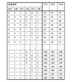
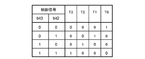
デコード回路620は、6ビットデジタル信号の上位4ビットのうちの下位2ビット(bit3及びbit2)を、いずれか1個が有効(論理値1)にされる4(=22)個の選択信号T3,T2,T1,T0にデコードする。図8は、このデコード回路620の動作を示している。
The
第1のスイッチ回路210は、17個の基準電圧V0〜V64のうち互いに隣接する2つの基準電圧(以下、低い方をVin1とし、高い方をVin2とする。)を選択する回路であって、6ビットデジタル信号のうちの上位2ビット(bit5及びbit4)と、デコード回路620からの選択信号T3,T2,T1,T0とを、制御信号として受け取る。
The
211は、T0によりオン/オフ制御されて、T0=1の場合に2入力(ノードn0及びn1の電圧)を2出力へ伝達する1個のスイッチ対である。212は、T1によりオン/オフ制御されて、T1=1の場合に2入力(ノードn1及びn2の電圧)を2出力へ伝達する1個のスイッチ対である。213は、T2によりオン/オフ制御されて、T2=1の場合に2入力(ノードn2及びn3の電圧)を2出力へ伝達する1個のスイッチ対である。214は、T3によりオン/オフ制御されて、T3=1の場合に2入力(ノードn3及びn4の電圧)を2出力へ伝達する1個のスイッチ対である。これら4(=22)個のスイッチ対211〜214は、各々デコード回路620からの4個の選択信号T3,T2,T1,T0のうちの対応する選択信号に従って2入力を2出力へ選択的に伝達するものであって、各々の上側出力が1共通出力に、各々の下側出力が他の1共通出力にそれぞれ接続されている。そして、これら2共通出力が第2のスイッチ回路320の2入力となる。
215は、bit4によりオン/オフ制御される5(=22+1)個の2入力・1出力スイッチ対である。これら5個のスイッチ対215の出力は、ノードn0,n1,n2,n3,n4の電圧である。216は、bit5によりオン/オフ制御される10(=5×2)個の2入力・1出力スイッチ対であって、基準電圧生成回路100から受け取った17個の基準電圧V0,V4,V8,…,V64のうちの10個の基準電圧をスイッチ対215へ与える。これら15個のスイッチ対215,216は、各々6ビットデジタル信号の上位2ビット(bit5及びbit4)のうちの対応ビットに従って2入力のうち一方を選択するものであって、対応ビットが0ならば下側入力を、対応ビットが1ならば上側入力をそれぞれ選択する。
以上のとおり、第1のスイッチ回路210は、19個のスイッチ対211〜216で構成されている。
As described above, the
例えば、bit5からbit2までの4ビットが“0000”ならば、第1のスイッチ回路210中の5個のノードn0,n1,n2,n3,n4にそれぞれ基準電圧V0,V4,V8,V12,V16が現れる。このうち、基準電圧生成回路100の最も低い基準電圧V0が3(=6−2−2+1)個のMOSトランジスタを通じて第2のスイッチ回路320に接続され、次に低い基準電圧V4が他の3個のMOSトランジスタを通じて第2のスイッチ回路320に接続される。この場合にはVin1=V0、Vin2=V4である。
For example, if 4 bits from bit 5 to
bit5からbit2までの4ビットが“0001”ならば、第1のスイッチ回路210中の5個のノードn0,n1,n2,n3,n4にそれぞれ基準電圧V0,V4,V8,V12,V16が現れる。このうち、基準電圧V4が3個のMOSトランジスタを通じて第2のスイッチ回路320に接続され、次に高い基準電圧V8が他の3個のMOSトランジスタを通じて第2のスイッチ回路320に接続される。この場合にはVin1=V4、Vin2=V8である。
If the 4 bits from bit 5 to
bit5からbit2までの4ビットが“1111”ならば、第1のスイッチ回路210中の5個のノードn0,n1,n2,n3,n4にそれぞれ基準電圧V48,V52,V56,V60,V64が現れる。このうち、基準電圧V60が3個のMOSトランジスタを通じて第2のスイッチ回路320に接続され、最も高い基準電圧V64が他の3個のMOSトランジスタを通じて第2のスイッチ回路320に接続される。この場合にはVin1=V60、Vin2=V64である。
If the 4 bits from bit 5 to
第2のスイッチ回路320は、図2中の第2のスイッチ回路300と同様の構成である。ただし、図7では、ノードn01とノードn02との間に直列接続されたMOSトランジスタM01の数と、ノードn02とノードn03との間に直列接続されたMOSトランジスタM02の数とがそれぞれ4(=6−2−2+2)である。例えばbit5からbit2までの4ビットが“0000”であり、かつM00、M01、M02及びM03の全てがオンしているとき、基準電圧V0とノードn01との間、ノードn01とノードn02との間、ノードn02とノードn03との間、ノードn03と基準電圧V4との間に、それぞれオン状態の4個のMOSトランジスタからなるMOSトランジスタ群が介在することになり、これら4個の互いに直列接続されたMOSトランジスタ群の各々の合成オン抵抗によりV0とV4との差が4分割されて、3個の中間電圧が得られる。なお、基準電圧V0とノードn01との間のMOSトランジスタ群は第1のスイッチ回路210中の3個のMOSトランジスタを、ノードn03と基準電圧V4との間のMOSトランジスタ群は第1のスイッチ回路210中の他の3個のMOSトランジスタをそれぞれ含む。
The
また、図7では、ノードn00とノードn00’との間に直列接続されたMOSトランジスタM00’の数と、ノードn03’とノードn04との間に直列接続されたMOSトランジスタM03’の数とがそれぞれ5(=6−2−2+3)であり、ノードn00’とノードn01との間に直列接続されたMOSトランジスタM01’の数と、ノードn03とノードn03’との間に接続されたMOSトランジスタM02’の数とがそれぞれ4(=6−2−2+2)である。例えばbit5からbit2までの4ビットが“1111”であり、かつM00’、M01’、M01、M02、M02’及びM03’の全てがオンし、かつM00及びM03がオフしているとき、基準電圧V60とノードn00’との間、ノードn00’とノードn02との間、ノードn02とノードn03’との間、ノードn03’と基準電圧V64との間に、それぞれオン状態の8個のMOSトランジスタからなるMOSトランジスタ群が介在することになり、これら4個の互いに直列接続されたMOSトランジスタ群の各々の合成オン抵抗によりV60とV64との差が4分割されて、3個の中間電圧が得られる。なお、基準電圧V60とノードn00’との間のMOSトランジスタ群は第1のスイッチ回路210中の3個のMOSトランジスタを、ノードn03’と基準電圧V64との間のMOSトランジスタ群は第1のスイッチ回路210中の他の3個のMOSトランジスタをそれぞれ含む。
In FIG. 7, the number of MOS transistors M00 ′ connected in series between the node n00 and the node n00 ′ and the number of MOS transistors M03 ′ connected in series between the node n03 ′ and the node n04 are as follows. Each is 5 (= 6-2-2 + 3), the number of MOS transistors M01 ′ connected in series between the node n00 ′ and the node n01, and the MOS transistors connected between the node n03 and the node n03 ′ The number of M02 ′ is 4 (= 6-2−2 + 2). For example, when 4 bits from bit 5 to
第3のスイッチ回路400、ボルテージフォロア500及び論理回路600は、いずれも図2で説明したものと同じ構成である。したがって、第2及び第3のスイッチ回路320,400の動作は図3及び図4と同様であり、図7のDACの全体動作は図5と同様である。
The
なお、6ビットデジタル信号の上位4ビットのうちの下位3ビット(bit4、bit3及びbit2)をデコード回路620にてデコードする場合には、8(=23)個の選択信号が得られるので、これらの選択信号をそれぞれ受け取る8個の2入力・2出力スイッチ対と、bit5によりオン/オフ制御される9(=23+1)個の2入力・1出力スイッチ対とを第1のスイッチ回路210に設ける。これに伴って、第2のスイッチ回路320では、ノードn01とノードn02との間のMOSトランジスタM01の数と、ノードn02とノードn03との間のMOSトランジスタM02の数とをそれぞれ3(=6−2−3+2)とする。また、ノードn00とノードn00’との間のMOSトランジスタM00’の数と、ノードn03’とノードn04との間のMOSトランジスタM03’の数とをそれぞれ4(=6−2−3+3)とし、ノードn00’とノードn01との間のMOSトランジスタM01’の数と、ノードn03とノードn03’との間のMOSトランジスタM02’の数とをそれぞれ3(=6−2−3+2)とする。
When the lower 3 bits (bit4, bit3, and bit2) of the upper 4 bits of the 6-bit digital signal are decoded by the
また、6ビットデジタル信号の上位4ビット(bit5、bit4、bit3及びbit2)の全てをデコード回路620にてデコードする場合には、16(=24)個の選択信号が得られるので、これらの選択信号をそれぞれ受け取る16個の2入力・2出力スイッチ対を第1のスイッチ回路210に設ける。これに伴って、第2のスイッチ回路320では、ノードn01とノードn02との間のMOSトランジスタM01の数と、ノードn02とノードn03との間のMOSトランジスタM02の数とをそれぞれ2(=6−2−4+2)とする。また、ノードn00とノードn00’との間のMOSトランジスタM00’の数と、ノードn03’とノードn04との間のMOSトランジスタM03’の数とをそれぞれ3(=6−2−4+3)とし、ノードn00’とノードn01との間のMOSトランジスタM01’の数と、ノードn03とノードn03’との間のMOSトランジスタM02’の数とをそれぞれ2(=6−2−4+2)とする。
In addition, when all the upper 4 bits (bit5, bit4, bit3, and bit2) of the 6-bit digital signal are decoded by the
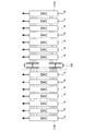
図9は、図1の画像表示装置1における基準電圧生成回路の構成例を示している。図9に示した基準電圧生成回路130は、2個の抵抗分圧回路を有する。一方の抵抗分圧回路は全DACのうち半分のDAC1100への基準電圧の供給を分担し、他方の抵抗分圧回路は他の半分のDAC1110への基準電圧の供給を分担する。このように各抵抗分圧回路の負担を軽減することにより、基準電圧の変動を抑制することができる。DAC1100,1110の各々は、前述のDACのうちのいずれかである。特に、多数のDACが同じ2基準電圧の組(前述のVin1及びVin2)を選択する場合に効果がある。
FIG. 9 shows a configuration example of the reference voltage generation circuit in the
以上説明してきたとおり、本発明に係るDACは、同じセトリング時間と同じ分解能とを維持しつつ構成素子数を削減することができ、液晶ディスプレイに限らず、有機ELディスプレイ等の画像表示装置用のDACとして有用である。 As described above, the DAC according to the present invention can reduce the number of constituent elements while maintaining the same settling time and the same resolution, and is not limited to a liquid crystal display, but for an image display device such as an organic EL display. Useful as a DAC.
1 画像表示装置
10 液晶ディスプレイパネル
11 TFT
12 画素容量
20 ゲートドライバ
25 ソースドライバ
30 コントローラ
100,130 基準電圧生成回路
200,210 第1のスイッチ回路(SW1)
300,320 第2のスイッチ回路(SW2)
400 第3のスイッチ回路(SW3)
500 ボルテージフォロア
600 論理回路
620 デコード回路
1100,1110 DAC
M00〜M07,M00’〜M07’ MOSトランジスタ
1
12
300, 320 Second switch circuit (SW2)
400 Third switch circuit (SW3)
500
M00 to M07, M00 'to M07' MOS transistors
Claims (11)
各々スイッチとして機能する複数のMOSトランジスタを有し、mを1以上の整数とし、2mから2m−1+1までの整数のうちのいずれかをMとするとき、前記デジタル信号のうちの上位(N−m)ビットに従って前記複数のMOSトランジスタのうち各々互いに同数のMOSトランジスタを通じて前記複数の基準電圧のうちの2つの基準電圧を選択し、かつ(M−1)個の中間電圧を得るように、前記選択された2つの基準電圧の差を、前記複数のMOSトランジスタのうち互いに直列接続されたM個のMOSトランジスタ群の各々の合成オン抵抗でM分割する選択分圧回路と、
前記選択分圧回路の前記M個のMOSトランジスタ群の各々の合成オン抵抗の大きさを判別し、当該合成オン抵抗が大きい場合には第1モードを、当該合成オン抵抗が小さい場合には第2モードをそれぞれ選択し、かつ前記選択分圧回路の前記M個のMOSトランジスタ群の各々に含まれるMOSトランジスタの個数が前記第1モードよりも前記第2モードの方が多くなるように制御するモード選択回路と、
前記デジタル信号のうちの下位mビットに従って、前記選択された2つの基準電圧のうちの1つ又は前記(M−1)個の中間電圧のうちの1つを前記アナログ信号として選択的に出力する出力回路とを備えたことを特徴とするコンバータ。 A converter that converts a digital signal of N (N is an integer of 3 or more) bits into an analog signal using a plurality of different reference voltages,
A plurality of MOS transistors which respectively function as a switch, when the m is an integer equal to or greater than 1, any of integers from 2 m to 2 m-1 +1 and M, the upper of said digital signal According to (N−m) bits, two reference voltages of the plurality of reference voltages are selected through the same number of MOS transistors among the plurality of MOS transistors, and (M−1) intermediate voltages are obtained. And a selection voltage dividing circuit that divides the difference between the selected two reference voltages into M by the combined on-resistance of each of the M MOS transistor groups connected in series among the plurality of MOS transistors,
The magnitude of the combined on-resistance of each of the M MOS transistor groups of the selective voltage dividing circuit is determined, and the first mode is selected when the combined on-resistance is large, and the first mode is selected when the combined on-resistance is small. Each of the two modes is selected and the number of MOS transistors included in each of the M MOS transistor groups of the selection voltage dividing circuit is controlled to be larger in the second mode than in the first mode. A mode selection circuit;
According to the lower m bits of the digital signal, one of the selected two reference voltages or one of the (M−1) intermediate voltages is selectively output as the analog signal. A converter comprising an output circuit.
前記複数の基準電圧を生成する基準電圧生成回路を更に備え、
前記基準電圧生成回路は、互いに直列接続された2N−m個の抵抗素子を有し、当該抵抗素子の各端子から互いに異なる(2N−m+1)個の基準電圧を前記選択分圧回路へ供給することを特徴とするコンバータ。 The converter of claim 1, wherein
A reference voltage generation circuit for generating the plurality of reference voltages;
The reference voltage generation circuit includes 2 N−m resistance elements connected in series to each other, and (2 N−m +1) different reference voltages from the respective terminals of the resistance elements are supplied to the selection voltage dividing circuit. A converter characterized by being supplied to.
前記選択分圧回路は、前記複数の基準電圧のうち互いに隣接する2つの基準電圧を選択するスイッチ回路を有することを特徴とするコンバータ。 The converter of claim 1, wherein
The converter, wherein the selection voltage dividing circuit includes a switch circuit that selects two reference voltages adjacent to each other among the plurality of reference voltages.
前記スイッチ回路は、各々前記デジタル信号の上位(N−m)ビットのうちの対応ビットに従って2入力のうち一方を選択する複数のスイッチ対を有し、
前記デジタル信号の上位(N−m)ビットのうち最下位ビットから数えてn番目のビットに対応するスイッチ対の数anは、
a1=2、an=an−1+2n−2(2≦n≦N−m)
にて与えられ、
前記複数のスイッチ対を構成するMOSトランジスタのうち各々(N−m)個のMOSトランジスタを通じて、前記互いに隣接する2つの基準電圧が選択されることを特徴とするコンバータ。 The converter of claim 3,
The switch circuit includes a plurality of switch pairs for selecting one of the two inputs according to corresponding bits of the upper (Nm) bits of the digital signal,
The number a n pairs of switches corresponding to the n-th bit counted from the upper (N-m) least significant bits of the bits of the digital signal,
a 1 = 2 and a n = a n−1 +2 n−2 (2 ≦ n ≦ N−m)
Given by
2. The converter according to claim 1, wherein the two reference voltages adjacent to each other are selected through (N−m) MOS transistors among the MOS transistors constituting the plurality of switch pairs.
前記選択分圧回路の前記M個のMOSトランジスタ群の各々は、互いに直列接続された(N−m+1)個以上のMOSトランジスタを有し、
前記M個のMOSトランジスタ群のうちの2つは、前記互いに直列接続された(N−m+1)個以上のMOSトランジスタの中に、前記互いに隣接する2つの基準電圧を選択するための(N−m)個のMOSトランジスタを含むことを特徴とするコンバータ。 The converter of claim 4, wherein
Each of the M MOS transistor groups of the selective voltage dividing circuit includes (N−m + 1) or more MOS transistors connected in series with each other,
Two of the M MOS transistor groups select (N−m + 1) for selecting two adjacent reference voltages among the (N−m + 1) or more MOS transistors connected in series to each other. m) A converter comprising a number of MOS transistors.
前記選択分圧回路は、Pを2以上かつ(N−m)以下の整数とするとき、前記デジタル信号の上位(N−m)ビットのうちの下位Pビットを、いずれか1個が有効にされる2P個の選択信号にデコードするデコード回路を更に有し、
前記スイッチ回路は、
各々前記2P個の選択信号のうちの対応する選択信号に従って2入力を2出力へ選択的に伝達する2P個のスイッチ対と、
各々前記デジタル信号の上位(N−m−P)ビットのうちの対応ビットに従って2入力のうち一方を選択する複数の他のスイッチ対とを有し、
前記全てのスイッチ対を構成するMOSトランジスタのうち各々(N−m−P+1)個のMOSトランジスタを通じて、前記互いに隣接する2つの基準電圧が選択されることを特徴とするコンバータ。 The converter of claim 3,
In the selection voltage dividing circuit, when P is an integer of 2 or more and (N−m) or less, any one of the lower P bits of the upper (N−m) bits of the digital signal is effective. A decoding circuit for decoding into 2 P selection signals to be
The switch circuit is
2 and P number of switch pairs for selectively transferring two inputs to two outputs in accordance each corresponding selection signal of said 2 P number of selection signals,
Each having a plurality of other switch pairs for selecting one of the two inputs according to the corresponding bit of the upper (NmP) bits of the digital signal;
2. The converter according to claim 1, wherein the two reference voltages adjacent to each other are selected through (Nm-P + 1) MOS transistors each of the MOS transistors constituting all the switch pairs.
前記選択分圧回路の前記M個のMOSトランジスタ群の各々は、互いに直列接続された(N−m−P+2)個以上のMOSトランジスタを有し、
前記M個のMOSトランジスタ群のうちの2つは、前記互いに直列接続された(N−m−P+2)個以上のMOSトランジスタの中に、前記互いに隣接する2つの基準電圧を選択するための(N−m−P+1)個のMOSトランジスタを含むことを特徴とするコンバータ。 The converter of claim 6, wherein
Each of the M MOS transistor groups of the selective voltage dividing circuit includes (N−m−P + 2) or more MOS transistors connected in series with each other,
Two of the M MOS transistor groups are for selecting two adjacent reference voltages among the (NmP + 2) or more MOS transistors connected in series with each other ( A converter comprising N−m−P + 1) MOS transistors.
前記選択分圧回路の前記M個のMOSトランジスタ群の各々に含まれるMOSトランジスタの個数は、当該M個のMOSトランジスタ群の各々の合成オン抵抗が互いに等しくなるように設定されたことを特徴とするコンバータ。 The converter of claim 1, wherein
The number of MOS transistors included in each of the M MOS transistor groups of the selective voltage dividing circuit is set so that the combined on-resistances of the M MOS transistor groups are equal to each other. Converter.
前記選択分圧回路の前記M個のMOSトランジスタ群の各々に含まれるMOSトランジスタのサイズは、当該M個のMOSトランジスタ群の各々の合成オン抵抗が互いに等しくなるように設定されたことを特徴とするコンバータ。 The converter of claim 1, wherein
The size of the MOS transistors included in each of the M MOS transistor groups of the selective voltage dividing circuit is set so that the combined on-resistances of the M MOS transistor groups are equal to each other. Converter.
前記駆動回路は、
互いに異なる複数の基準電圧を生成する基準電圧生成回路と、
前記複数の基準電圧を用いて前記画像の階調を表すデジタル信号を画素列毎のアナログ信号に変換する複数のデジタル・アナログコンバータとを備え、
前記複数のデジタル・アナログコンバータの各々は、請求項1記載のコンバータであることを特徴とする画像表示装置。 An image display device comprising: a display panel having a plurality of pixels; and a drive circuit that drives the plurality of pixels in accordance with a digital signal representing a gradation of an image,
The drive circuit is
A reference voltage generation circuit for generating a plurality of different reference voltages;
A plurality of digital / analog converters for converting a digital signal representing the gradation of the image into an analog signal for each pixel column using the plurality of reference voltages;
The image display apparatus according to claim 1, wherein each of the plurality of digital / analog converters is a converter according to claim 1.
前記基準電圧生成回路は、各々前記画素列毎のコンバータの一部への基準電圧の供給を分担する複数の抵抗分圧回路を有することを特徴とする画像表示装置。 The image display device according to claim 10.
The image display apparatus, wherein the reference voltage generation circuit includes a plurality of resistance voltage dividing circuits each sharing supply of a reference voltage to a part of the converter for each pixel column.
Priority Applications (3)
| Application Number | Priority Date | Filing Date | Title |
|---|---|---|---|
| JP2008007957A JP2009171298A (en) | 2008-01-17 | 2008-01-17 | Digital-to-analog converter |
| US12/236,038 US7671775B2 (en) | 2008-01-17 | 2008-09-23 | Digital-to-analog converter |
| CNA2008101902106A CN101488757A (en) | 2008-01-17 | 2008-12-26 | Digital-to-analog converter |
Applications Claiming Priority (1)
| Application Number | Priority Date | Filing Date | Title |
|---|---|---|---|
| JP2008007957A JP2009171298A (en) | 2008-01-17 | 2008-01-17 | Digital-to-analog converter |
Publications (1)
| Publication Number | Publication Date |
|---|---|
| JP2009171298A true JP2009171298A (en) | 2009-07-30 |
Family
ID=40876053
Family Applications (1)
| Application Number | Title | Priority Date | Filing Date |
|---|---|---|---|
| JP2008007957A Withdrawn JP2009171298A (en) | 2008-01-17 | 2008-01-17 | Digital-to-analog converter |
Country Status (3)
| Country | Link |
|---|---|
| US (1) | US7671775B2 (en) |
| JP (1) | JP2009171298A (en) |
| CN (1) | CN101488757A (en) |
Cited By (3)
| Publication number | Priority date | Publication date | Assignee | Title |
|---|---|---|---|---|
| JP2014197770A (en) * | 2013-03-29 | 2014-10-16 | ローム株式会社 | D/a converter |
| CN104517573A (en) * | 2014-08-25 | 2015-04-15 | 上海华虹宏力半导体制造有限公司 | Bias voltage generating circuit and liquid crystal drive circuit |
| JP2016144213A (en) * | 2015-02-02 | 2016-08-08 | 三星電子株式会社Samsung Electronics Co.,Ltd. | Laser detector using latch and semiconductor device including the same |
Families Citing this family (4)
| Publication number | Priority date | Publication date | Assignee | Title |
|---|---|---|---|---|
| KR101081356B1 (en) * | 2009-10-27 | 2011-11-08 | 주식회사 실리콘웍스 | Liquid Crystal Display Panel Driving Circuit |
| CN103546156B (en) * | 2012-07-10 | 2016-06-22 | 联咏科技股份有限公司 | Digital analog converter and source driving chip thereof |
| TWI618364B (en) * | 2015-08-31 | 2018-03-11 | 矽創電子股份有限公司 | Digital-to-analog converter and source driving circuit |
| CN111435588B (en) * | 2019-01-15 | 2022-05-13 | 深圳通锐微电子技术有限公司 | Drive circuit and display device |
Family Cites Families (10)
| Publication number | Priority date | Publication date | Assignee | Title |
|---|---|---|---|---|
| US5969657A (en) * | 1997-07-22 | 1999-10-19 | Analog Devices, Inc. | Digital to analog converter |
| US5877717A (en) * | 1997-12-15 | 1999-03-02 | Industrial Technology Research Institute | D/A converter with a Gamma correction circuit |
| JP3506219B2 (en) * | 1998-12-16 | 2004-03-15 | シャープ株式会社 | DA converter and liquid crystal driving device using the same |
| US6225931B1 (en) * | 1999-08-30 | 2001-05-01 | Industrial Technology Research Institute | D/A converter with a gamma correction circuit |
| JP3594125B2 (en) * | 2000-07-25 | 2004-11-24 | シャープ株式会社 | DA converter and liquid crystal driving device using the same |
| JP3493187B2 (en) * | 2001-06-13 | 2004-02-03 | 松下電器産業株式会社 | Successive approximation type A / D converter |
| JP4623712B2 (en) * | 2004-07-02 | 2011-02-02 | ルネサスエレクトロニクス株式会社 | Gradation voltage selection circuit, driver circuit, liquid crystal drive circuit, liquid crystal display device |
| JP4690105B2 (en) * | 2005-04-26 | 2011-06-01 | パナソニック株式会社 | Successive approximation type A / D converter |
| JP4836574B2 (en) * | 2005-12-28 | 2011-12-14 | オンセミコンダクター・トレーディング・リミテッド | Analog-to-digital converter and threshold correction method |
| JP2008160782A (en) * | 2006-01-31 | 2008-07-10 | Matsushita Electric Ind Co Ltd | Digital-to-analog converter |
-
2008
- 2008-01-17 JP JP2008007957A patent/JP2009171298A/en not_active Withdrawn
- 2008-09-23 US US12/236,038 patent/US7671775B2/en not_active Expired - Fee Related
- 2008-12-26 CN CNA2008101902106A patent/CN101488757A/en active Pending
Cited By (3)
| Publication number | Priority date | Publication date | Assignee | Title |
|---|---|---|---|---|
| JP2014197770A (en) * | 2013-03-29 | 2014-10-16 | ローム株式会社 | D/a converter |
| CN104517573A (en) * | 2014-08-25 | 2015-04-15 | 上海华虹宏力半导体制造有限公司 | Bias voltage generating circuit and liquid crystal drive circuit |
| JP2016144213A (en) * | 2015-02-02 | 2016-08-08 | 三星電子株式会社Samsung Electronics Co.,Ltd. | Laser detector using latch and semiconductor device including the same |
Also Published As
| Publication number | Publication date |
|---|---|
| US20090184856A1 (en) | 2009-07-23 |
| CN101488757A (en) | 2009-07-22 |
| US7671775B2 (en) | 2010-03-02 |
Similar Documents
| Publication | Publication Date | Title |
|---|---|---|
| US7423572B2 (en) | Digital-to-analog converter | |
| JP4639153B2 (en) | Digital / analog converter | |
| KR101421705B1 (en) | Reduced component digital to analog decoder and method | |
| JP2009171298A (en) | Digital-to-analog converter | |
| JP4661324B2 (en) | Digital analog circuit, data driver and display device | |
| JP5607815B2 (en) | DIGITAL / ANALOG CONVERSION CIRCUIT AND DISPLAY DEVICE DATA DRIVER | |
| JP5508978B2 (en) | Digital-analog conversion circuit and display driver | |
| US6344814B1 (en) | Driving circuit | |
| US8111184B2 (en) | Digital-to-analog converting circuit, data driver and display device | |
| JP2006310989A (en) | D/a conversion circuit, display driver, and display device | |
| US7245283B2 (en) | LCD source driving circuit having reduced structure including multiplexing-latch circuits | |
| US20070200816A1 (en) | Decoder circuit having level shifting function and liquid crystal drive device using decoder circuit | |
| JP5627085B2 (en) | Semiconductor device including level shifter, display device, and operation method thereof | |
| JP5329465B2 (en) | Level voltage selection circuit, data driver and display device | |
| KR100789700B1 (en) | Digital to analog converter including the pseudo segment resistor cell | |
| JP2011135150A (en) | D/a converter circuit, and voltage supply control method therefor | |
| US9209823B2 (en) | Decoder level shifter device and digital to analog converter using the same | |
| JP2008111917A (en) | Voltage selecting circuit, drive circuit, electro-optical device, and electronic equipment | |
| JP2013218021A (en) | Data driver device and display device | |
| JP2009258237A (en) | Liquid crystal driving device | |
| JP2007226173A (en) | Digital data driver and display device using same | |
| JP2006173779A (en) | Digital/analog conversion circuit and display | |
| JP2005301209A (en) | Gate driver circuit of thin-film transistor liquid crystal display | |
| KR100915092B1 (en) | Source driver for TFT-LCD | |
| CN117789652A (en) | Digital-to-analog conversion circuit, data driver and display device |
Legal Events
| Date | Code | Title | Description |
|---|---|---|---|
| A621 | Written request for application examination |
Free format text: JAPANESE INTERMEDIATE CODE: A621 Effective date: 20100831 |
|
| RD02 | Notification of acceptance of power of attorney |
Free format text: JAPANESE INTERMEDIATE CODE: A7422 Effective date: 20120130 |
|
| A761 | Written withdrawal of application |
Free format text: JAPANESE INTERMEDIATE CODE: A761 Effective date: 20120201 |