JP2009155672A - Method for manufacturing group-iii nitride semiconductor, method for manufacturing light-emitting device of group-iii nitride semiconductor, apparatus for manufacturing group-iii nitride semiconductor, group-iii nitride semiconductor and light-emitting device of group-iii nitride semiconductor, and lamp - Google Patents
Method for manufacturing group-iii nitride semiconductor, method for manufacturing light-emitting device of group-iii nitride semiconductor, apparatus for manufacturing group-iii nitride semiconductor, group-iii nitride semiconductor and light-emitting device of group-iii nitride semiconductor, and lamp Download PDFInfo
- Publication number
- JP2009155672A JP2009155672A JP2007332678A JP2007332678A JP2009155672A JP 2009155672 A JP2009155672 A JP 2009155672A JP 2007332678 A JP2007332678 A JP 2007332678A JP 2007332678 A JP2007332678 A JP 2007332678A JP 2009155672 A JP2009155672 A JP 2009155672A
- Authority
- JP
- Japan
- Prior art keywords
- iii nitride
- layer
- nitride semiconductor
- group iii
- chamber
- Prior art date
- Legal status (The legal status is an assumption and is not a legal conclusion. Google has not performed a legal analysis and makes no representation as to the accuracy of the status listed.)
- Pending
Links
Images


Classifications
-
- H—ELECTRICITY
- H01—ELECTRIC ELEMENTS
- H01L—SEMICONDUCTOR DEVICES NOT COVERED BY CLASS H10
- H01L2224/00—Indexing scheme for arrangements for connecting or disconnecting semiconductor or solid-state bodies and methods related thereto as covered by H01L24/00
- H01L2224/01—Means for bonding being attached to, or being formed on, the surface to be connected, e.g. chip-to-package, die-attach, "first-level" interconnects; Manufacturing methods related thereto
- H01L2224/26—Layer connectors, e.g. plate connectors, solder or adhesive layers; Manufacturing methods related thereto
- H01L2224/31—Structure, shape, material or disposition of the layer connectors after the connecting process
- H01L2224/32—Structure, shape, material or disposition of the layer connectors after the connecting process of an individual layer connector
- H01L2224/321—Disposition
- H01L2224/32151—Disposition the layer connector connecting between a semiconductor or solid-state body and an item not being a semiconductor or solid-state body, e.g. chip-to-substrate, chip-to-passive
- H01L2224/32221—Disposition the layer connector connecting between a semiconductor or solid-state body and an item not being a semiconductor or solid-state body, e.g. chip-to-substrate, chip-to-passive the body and the item being stacked
- H01L2224/32245—Disposition the layer connector connecting between a semiconductor or solid-state body and an item not being a semiconductor or solid-state body, e.g. chip-to-substrate, chip-to-passive the body and the item being stacked the item being metallic
-
- H—ELECTRICITY
- H01—ELECTRIC ELEMENTS
- H01L—SEMICONDUCTOR DEVICES NOT COVERED BY CLASS H10
- H01L2224/00—Indexing scheme for arrangements for connecting or disconnecting semiconductor or solid-state bodies and methods related thereto as covered by H01L24/00
- H01L2224/01—Means for bonding being attached to, or being formed on, the surface to be connected, e.g. chip-to-package, die-attach, "first-level" interconnects; Manufacturing methods related thereto
- H01L2224/42—Wire connectors; Manufacturing methods related thereto
- H01L2224/47—Structure, shape, material or disposition of the wire connectors after the connecting process
- H01L2224/48—Structure, shape, material or disposition of the wire connectors after the connecting process of an individual wire connector
- H01L2224/4805—Shape
- H01L2224/4809—Loop shape
- H01L2224/48091—Arched
-
- H—ELECTRICITY
- H01—ELECTRIC ELEMENTS
- H01L—SEMICONDUCTOR DEVICES NOT COVERED BY CLASS H10
- H01L2224/00—Indexing scheme for arrangements for connecting or disconnecting semiconductor or solid-state bodies and methods related thereto as covered by H01L24/00
- H01L2224/01—Means for bonding being attached to, or being formed on, the surface to be connected, e.g. chip-to-package, die-attach, "first-level" interconnects; Manufacturing methods related thereto
- H01L2224/42—Wire connectors; Manufacturing methods related thereto
- H01L2224/47—Structure, shape, material or disposition of the wire connectors after the connecting process
- H01L2224/48—Structure, shape, material or disposition of the wire connectors after the connecting process of an individual wire connector
- H01L2224/481—Disposition
- H01L2224/48151—Connecting between a semiconductor or solid-state body and an item not being a semiconductor or solid-state body, e.g. chip-to-substrate, chip-to-passive
- H01L2224/48221—Connecting between a semiconductor or solid-state body and an item not being a semiconductor or solid-state body, e.g. chip-to-substrate, chip-to-passive the body and the item being stacked
- H01L2224/48245—Connecting between a semiconductor or solid-state body and an item not being a semiconductor or solid-state body, e.g. chip-to-substrate, chip-to-passive the body and the item being stacked the item being metallic
- H01L2224/48247—Connecting between a semiconductor or solid-state body and an item not being a semiconductor or solid-state body, e.g. chip-to-substrate, chip-to-passive the body and the item being stacked the item being metallic connecting the wire to a bond pad of the item
-
- H—ELECTRICITY
- H01—ELECTRIC ELEMENTS
- H01L—SEMICONDUCTOR DEVICES NOT COVERED BY CLASS H10
- H01L2224/00—Indexing scheme for arrangements for connecting or disconnecting semiconductor or solid-state bodies and methods related thereto as covered by H01L24/00
- H01L2224/01—Means for bonding being attached to, or being formed on, the surface to be connected, e.g. chip-to-package, die-attach, "first-level" interconnects; Manufacturing methods related thereto
- H01L2224/42—Wire connectors; Manufacturing methods related thereto
- H01L2224/47—Structure, shape, material or disposition of the wire connectors after the connecting process
- H01L2224/48—Structure, shape, material or disposition of the wire connectors after the connecting process of an individual wire connector
- H01L2224/481—Disposition
- H01L2224/48151—Connecting between a semiconductor or solid-state body and an item not being a semiconductor or solid-state body, e.g. chip-to-substrate, chip-to-passive
- H01L2224/48221—Connecting between a semiconductor or solid-state body and an item not being a semiconductor or solid-state body, e.g. chip-to-substrate, chip-to-passive the body and the item being stacked
- H01L2224/48245—Connecting between a semiconductor or solid-state body and an item not being a semiconductor or solid-state body, e.g. chip-to-substrate, chip-to-passive the body and the item being stacked the item being metallic
- H01L2224/48257—Connecting between a semiconductor or solid-state body and an item not being a semiconductor or solid-state body, e.g. chip-to-substrate, chip-to-passive the body and the item being stacked the item being metallic connecting the wire to a die pad of the item
-
- H—ELECTRICITY
- H01—ELECTRIC ELEMENTS
- H01L—SEMICONDUCTOR DEVICES NOT COVERED BY CLASS H10
- H01L2224/00—Indexing scheme for arrangements for connecting or disconnecting semiconductor or solid-state bodies and methods related thereto as covered by H01L24/00
- H01L2224/73—Means for bonding being of different types provided for in two or more of groups H01L2224/10, H01L2224/18, H01L2224/26, H01L2224/34, H01L2224/42, H01L2224/50, H01L2224/63, H01L2224/71
- H01L2224/732—Location after the connecting process
- H01L2224/73251—Location after the connecting process on different surfaces
- H01L2224/73265—Layer and wire connectors
-
- H—ELECTRICITY
- H01—ELECTRIC ELEMENTS
- H01L—SEMICONDUCTOR DEVICES NOT COVERED BY CLASS H10
- H01L2924/00—Indexing scheme for arrangements or methods for connecting or disconnecting semiconductor or solid-state bodies as covered by H01L24/00
- H01L2924/30—Technical effects
- H01L2924/301—Electrical effects
- H01L2924/3011—Impedance
-
- H—ELECTRICITY
- H01—ELECTRIC ELEMENTS
- H01L—SEMICONDUCTOR DEVICES NOT COVERED BY CLASS H10
- H01L2924/00—Indexing scheme for arrangements or methods for connecting or disconnecting semiconductor or solid-state bodies as covered by H01L24/00
- H01L2924/30—Technical effects
- H01L2924/301—Electrical effects
- H01L2924/3025—Electromagnetic shielding
Abstract
Description
本発明は、発光ダイオード(LED)、レーザダイオード(LD)、電子デバイス等に、好適に用いられ、一般式AlaGabIncN(0≦a≦1、0≦b≦1、0≦c≦1、a+b+c=1)で表されるIII族窒化物半導体の製造方法、III族窒化物半導体発光素子の製造方法、及びIII族窒化物半導体発光素子、並びにランプに関する。 The present invention is a light emitting diode (LED), a laser diode (LD), a electronic device, etc., suitably used, formula Al a Ga b In c N ( 0 ≦ a ≦ 1,0 ≦ b ≦ 1,0 ≦ The present invention relates to a group III nitride semiconductor manufacturing method, a group III nitride semiconductor light emitting device manufacturing method, a group III nitride semiconductor light emitting device, and a lamp represented by c ≦ 1, a + b + c = 1).
III族窒化物半導体は、可視光から紫外光領域の範囲に相当するエネルギーの直接遷移型のバンドギャップを有し、発光効率に優れていることから、発光ダイオード(LED)やレーザダイオード(LD)等の半導体発光素子として製品化され、各種用途で使用されている。また、電子デバイスに用いた場合でも、III族窒化物半導体は、従来のIII−V族化合物半導体を用いた場合に比べて優れた特性が得られるポテンシャルを有している。 Group III nitride semiconductors have a direct transition type band gap of energy corresponding to the range from visible light to ultraviolet light, and are excellent in luminous efficiency. Therefore, light emitting diodes (LEDs) and laser diodes (LDs) It is commercialized as a semiconductor light emitting device such as, and is used in various applications. Even when used in an electronic device, the group III nitride semiconductor has a potential for obtaining superior characteristics as compared with the case of using a conventional group III-V compound semiconductor.
このようなIII族窒化物半導体は、一般的に、トリメチルガリウム、トリメチルアルミニウムおよびアンモニアを原料として、有機金属化学気相成長(MOCVD)法によって製造されている。MOCVD法は、キャリアガスに原料の蒸気を含ませて基板表面に運搬し、加熱された基板との反応で原料を分解させることにより、結晶を成長させる方法である。また、従来、III族窒化物半導体の単結晶ウェーハは市販されておらず、III族窒化物半導体としては、異なる材料の単結晶ウェーハ上に結晶を成長させて得る方法が一般的である。 Such group III nitride semiconductors are generally manufactured by metal organic chemical vapor deposition (MOCVD) using trimethylgallium, trimethylaluminum and ammonia as raw materials. The MOCVD method is a method in which a vapor of a raw material is contained in a carrier gas and transported to the substrate surface, and the raw material is decomposed by reaction with a heated substrate to grow crystals. Conventionally, group III nitride semiconductor single crystal wafers are not commercially available, and group III nitride semiconductors are generally obtained by growing crystals on single crystal wafers of different materials.
上述したようなIII族窒化物半導体の成長方法としては、有機金属化学気相成長(MOCVD)法により、サファイア単結晶基板もしくはSiC単結晶基板の上に、III族窒化物半導体結晶をエピタキシャル成長させる際、まず、基板上に窒化アルミニウム(AlN)や窒化アルミニウムガリウム(AlGaN)からなる低温バッファ層と呼ばれる層を積層し、その上に高温でIII族窒化物半導体結晶をエピタキシャル成長させる方法が提案されており、一般に行われている(例えば、特許文献1、2)。
また、上記バッファ層をMOCVD以外の方法で成膜する技術も提案されており、例えば、高周波スパッタで成膜したバッファ層上に、MOCVDによって同じ組成の結晶を成長させる方法が提案されている(例えば、特許文献3)。
As a method for growing a group III nitride semiconductor as described above, a group III nitride semiconductor crystal is epitaxially grown on a sapphire single crystal substrate or a SiC single crystal substrate by metal organic chemical vapor deposition (MOCVD). First, a method is proposed in which a layer called a low-temperature buffer layer made of aluminum nitride (AlN) or aluminum gallium nitride (AlGaN) is stacked on a substrate, and a group III nitride semiconductor crystal is epitaxially grown at a high temperature on the layer. Is generally performed (for example, Patent Documents 1 and 2).
In addition, a technique for forming the buffer layer by a method other than MOCVD has been proposed. For example, a method of growing crystals of the same composition by MOCVD on a buffer layer formed by high-frequency sputtering has been proposed ( For example, Patent Document 3).
また、III族窒化物半導体結晶をスパッタ法によって製造する研究も行われており、例えば、高抵抗のGaNを積層することを目的とし、サファイア基板上に、スパッタ法によってGaNを直接成膜する方法が提案されている(例えば、特許文献4)。スパッタ法を用いてGaNを成膜する場合、上記特許文献1〜3に記載されたようなMOCVD法を用いた方法に比べ、設備が安価で済むことや、工程が安定化し、生産効率が向上する等の利点がある。
反応性スパッタ法によってIII族窒化物半導体からなる半導体層を成膜する場合、基板の温度を、例えば700℃以上の高温に保持しながら制御し、規定の成膜条件を常に再現することが重要となる。
しかしながら、本発明者等が鋭意研究したところ、上記特許文献1〜4に記載されたような、従来のスパッタ装置及び方法によってGaNからなる結晶を成膜する場合、高温とされた基板をチャンバ内に配置すると、チャンバの内壁に付着していたデポ物が、基板からの輻射熱を受けて高温となったり或いはプラズマによって衝撃を受けたりすることにより、活性な窒素がチャンバ内に放出されることが明らかとなった。
このような場合、チャンバ内に放出される活性な窒素原子も、基板上へのGaN結晶の成膜反応に寄与するため、成膜に用いられるGa元素と窒素(N2)の実質的な反応比率を制御することができず、規定の成膜条件を常に再現することが困難となっていた。さらに、成膜の開始時と終了時ではIII族元素と窒素との比率に変化が生じることや、成膜処理を重ねる毎にチャンバ内におけるデポジション等の堆積が進行し、最適な成膜条件の再現が出来ないこと等も原因に挙げられる。
When forming a semiconductor layer made of a group III nitride semiconductor by reactive sputtering, it is important to control the substrate temperature while maintaining it at a high temperature of, for example, 700 ° C. or higher, and always reproduce the specified film formation conditions. It becomes.
However, as a result of diligent researches by the present inventors, when a GaN crystal is formed by a conventional sputtering apparatus and method as described in Patent Documents 1 to 4, a substrate at a high temperature is placed in the chamber. In this case, the deposit attached to the inner wall of the chamber is heated by receiving radiation heat from the substrate or is subjected to an impact by plasma, so that active nitrogen may be released into the chamber. It became clear.
In such a case, since active nitrogen atoms released into the chamber also contribute to the film formation reaction of the GaN crystal on the substrate, a substantial reaction between the Ga element used for film formation and nitrogen (N 2 ). The ratio could not be controlled, and it was difficult to always reproduce the prescribed film forming conditions. Furthermore, at the start and end of film formation, the ratio between the group III element and nitrogen changes, and deposition and other deposition progresses in the chamber each time the film formation process is repeated. Another reason is that it cannot be reproduced.
反応性スパッタ法によって成膜されるIII族窒化物半導体の優れた結晶性と良好な表面状態を両立させるためには、Ga元素と窒素の比率は重要なパラメータとなる。窒素の比率が高すぎる場合には、成膜されるGaN結晶内に多くのGaの欠損が生じ、黄色みを帯びた結晶となり、結晶性の低いものとなる。一方、Gaの比率が高い場合には、成膜されるGaN結晶の表面にメタルドロップレットが生じ、平坦な表面にならないという問題がある。このため、製造工程における歩留まりの低下や、ひいては、GaN層(III族窒化物半導体)が用いられてなる発光素子等の各種素子の特性低下が生じる虞があった。
このため、反応性スパッタ法によってIII族窒化物半導体の結晶を成膜する際、チャンバ内におけるGaと窒素との比率を安定させ、良好な特性を有するIII族窒化物半導体の層を、高効率で安定して基板上に成膜することが可能な方法及び装置が望まれていた。
In order to achieve both excellent crystallinity and a good surface state of a group III nitride semiconductor film formed by reactive sputtering, the ratio of Ga element and nitrogen is an important parameter. When the ratio of nitrogen is too high, many Ga defects are generated in the deposited GaN crystal, resulting in a yellowish crystal with low crystallinity. On the other hand, when the Ga ratio is high, metal droplets are generated on the surface of the GaN crystal to be formed, and there is a problem that the surface is not flat. For this reason, there is a possibility that the yield in the manufacturing process is lowered and, as a result, the characteristics of various elements such as a light emitting element using a GaN layer (group III nitride semiconductor) are lowered.
For this reason, when a group III nitride semiconductor crystal is formed by reactive sputtering, the ratio of Ga and nitrogen in the chamber is stabilized, and a group III nitride semiconductor layer having good characteristics can be obtained with high efficiency. Thus, there has been a demand for a method and an apparatus capable of stably forming a film on a substrate.
本発明は上記問題に鑑みてなされたものであり、良好な膜質を有するIII族窒化物半導体を反応性スパッタ法によって効率よく成膜することができるIII族窒化物半導体の製造方法及びIII族窒化物半導体製造装置、並びにIII族窒化物半導体発光素子の製造方法を提供することを目的とする。
さらに、上記製造方法によって得られ、発光特性に優れたIII族窒化物半導体発光素子並びにランプを提供することを目的とする。
The present invention has been made in view of the above problems, and a method for producing a group III nitride semiconductor and a group III nitride capable of efficiently forming a group III nitride semiconductor having good film quality by a reactive sputtering method. An object of the present invention is to provide a manufacturing method of a semiconductor light emitting device and a group III nitride semiconductor light emitting device.
Furthermore, it aims at providing the group III nitride semiconductor light-emitting device and lamp which were obtained by the said manufacturing method and were excellent in the light emission characteristic.
本発明者等は、上記問題を解決するために鋭意検討した結果、以下に示す発明を完成した。 As a result of intensive investigations to solve the above problems, the present inventors have completed the invention shown below.
[1] チャンバ内に基板及びGa元素を含有するターゲットを配置するとともに、反応ガス供給手段によって前記チャンバ内に窒素原子含有ガス及び不活性ガスを供給し、前記基板上に単結晶のIII族窒化物半導体をプラズマによる反応性スパッタ法で形成するIII族窒化物半導体の製造方法であって、前記チャンバ内の圧力を圧力モニタで検知し、該圧力モニタの検知信号に基づき、前記反応ガス供給手段から前記チャンバ内に供給する窒素原子含有ガスの流通量を流量制御手段によって制御することを特徴とするIII族窒化物半導体の製造方法。
[2] 前記III族窒化物半導体を形成する際の前記チャンバ内が、前記窒素原子含有ガスが20〜80%の範囲で含有され、残部が少なくとも不活性ガスを含有するガス雰囲気とされていることを特徴とする上記[1]に記載のIII族窒化物半導体の製造方法。
[3] 前記窒素原子含有ガスが窒素ガス(N2)とされ、前記不活性ガスがアルゴンガス(Ar)とされていることを特徴とする上記[1]又は[2]に記載のIII族窒化物半導体の製造方法。
[1] A substrate and a target containing Ga element are arranged in the chamber, and a nitrogen atom-containing gas and an inert gas are supplied into the chamber by a reaction gas supply means, and a single crystal group III nitride is formed on the substrate. A method for producing a group III nitride semiconductor in which a physical semiconductor is formed by a reactive sputtering method using plasma, wherein the pressure in the chamber is detected by a pressure monitor, and the reactive gas supply means is based on a detection signal of the pressure monitor A flow rate of a nitrogen atom-containing gas supplied into the chamber is controlled by a flow rate control means.
[2] The inside of the chamber at the time of forming the group III nitride semiconductor is a gas atmosphere containing the nitrogen atom-containing gas in a range of 20 to 80% and the balance containing at least an inert gas. The method for producing a group III nitride semiconductor as described in [1] above.
[3] The group III according to [1] or [2], wherein the nitrogen atom-containing gas is nitrogen gas (N 2 ) and the inert gas is argon gas (Ar) A method for manufacturing a nitride semiconductor.
[4] 前記III族窒化物半導体を形成する際の、前記基板の温度が600℃〜1050℃の範囲とされていることを特徴とする上記[1]〜[3]の何れか1項に記載のIII族窒化物半導体の製造方法。
[5] 前記III族窒化物半導体を形成する際の前記チャンバ内の圧力が0.01〜10Paの範囲であることを特徴とする上記[1]〜[4]の何れか1項に記載のIII族窒化物半導体の製造方法。
[4] In any one of the above [1] to [3], the temperature of the substrate when forming the group III nitride semiconductor is in a range of 600 ° C. to 1050 ° C. The manufacturing method of the group III nitride semiconductor of description.
[5] The pressure described in any one of [1] to [4], wherein the pressure in the chamber when forming the group III nitride semiconductor is in a range of 0.01 to 10 Pa. A method for producing a group III nitride semiconductor.
[6] 基板上に、少なくともIII族窒化物半導体から各々なるn型半導体層、発光層及びp型半導体層を順次積層して半導体層を形成するIII族窒化物半導体発光素子の製造方法であって、前記半導体層の少なくとも一部を、上記[1]〜[5]の何れか1項に記載のIII族窒化物半導体の製造方法によって形成することを特徴とするIII族窒化物半導体発光素子の製造方法。
[7] 上記[1]〜[5]の何れか1項に記載の製造方法によって製造されるIII族窒化物半導体。
[8] 上記[6]に記載の製造方法によって得られるIII族窒化物半導体発光素子。
[6] A method for manufacturing a group III nitride semiconductor light-emitting device, in which a semiconductor layer is formed by sequentially laminating an n-type semiconductor layer, a light-emitting layer, and a p-type semiconductor layer each made of at least a group III nitride semiconductor on a substrate. And at least a part of the semiconductor layer is formed by the Group III nitride semiconductor manufacturing method according to any one of [1] to [5] above. Manufacturing method.
[7] A group III nitride semiconductor manufactured by the manufacturing method according to any one of [1] to [5].
[8] A group III nitride semiconductor light-emitting device obtained by the production method according to the above [6].
[9] 上記[8]に記載のIII族窒化物半導体発光素子が用いられてなるランプ。
[10] チャンバ内に基板及びGa元素を含有するターゲットを配置するとともに、前記チャンバ内に窒素原子含有ガス及び不活性ガスを供給する反応ガス供給手段を備え、前記基板上に単結晶のIII族窒化物半導体をプラズマによる反応性スパッタ法で形成するIII族窒化物半導体製造装置であって、前記チャンバ内の圧力を検知する圧力モニタが備えられているとともに、該圧力モニタの検知信号に基づき、前記反応ガス供給手段から前記チャンバ内に供給される窒素原子含有ガスの流通量を制御する流量制御手段が備えられていることを特徴とするIII族窒化物半導体製造装置。
[9] A lamp comprising the group III nitride semiconductor light-emitting device according to [8].
[10] A substrate and a target containing Ga element are arranged in the chamber, and a reactive gas supply means for supplying a nitrogen atom-containing gas and an inert gas is provided in the chamber, and a single crystal group III is provided on the substrate. A group III nitride semiconductor manufacturing apparatus for forming a nitride semiconductor by a reactive sputtering method using plasma, provided with a pressure monitor for detecting the pressure in the chamber, and based on a detection signal of the pressure monitor, A group III nitride semiconductor manufacturing apparatus comprising flow rate control means for controlling a flow rate of nitrogen atom-containing gas supplied from the reaction gas supply means into the chamber.
本発明のIII族窒化物半導体の製造方法によれば、チャンバ内の圧力を圧力モニタで検知し、該圧力モニタの検知信号に基づき、反応ガス供給手段からチャンバ内に供給する窒素原子含有ガスの流通量を流量制御手段によって制御する方法なので、チャンバ内に存在する活性な窒素の量に応じて、この活性窒素の量が一定になるように窒素原子含有ガスの供給量を制御することができ、常に同一のスパッタ成膜条件を得ることが可能となる。これにより、チャンバ内におけるGaと窒素との比率を安定させ、良好な特性を有するIII族窒化物半導体層を、高効率で安定して基板上に成膜することが可能となる。 According to the Group III nitride semiconductor manufacturing method of the present invention, the pressure in the chamber is detected by the pressure monitor, and the nitrogen atom-containing gas supplied from the reaction gas supply means into the chamber is detected based on the detection signal of the pressure monitor. Since the flow rate is controlled by the flow rate control means, the supply amount of the nitrogen atom-containing gas can be controlled so that the amount of active nitrogen is constant according to the amount of active nitrogen present in the chamber. Therefore, it is possible to always obtain the same sputter deposition conditions. As a result, the ratio of Ga and nitrogen in the chamber can be stabilized, and a group III nitride semiconductor layer having good characteristics can be formed on the substrate with high efficiency and stability.
また、本発明のIII族窒化物半導体発光素子の製造方法によれば、半導体層の少なくとも一部を、上記製造方法により、単結晶のIII族窒化物半導体で形成する方法としているので、結晶性の良好なIII族窒化物半導体からなる半導体層を備え、優れた発光特性を有するIII族窒化物半導体発光素子が得られる。 Further, according to the method for manufacturing a group III nitride semiconductor light emitting device of the present invention, since at least a part of the semiconductor layer is formed of a single crystal group III nitride semiconductor by the above manufacturing method, A Group III nitride semiconductor light-emitting device having a semiconductor layer made of a good Group III nitride semiconductor and having excellent light emission characteristics can be obtained.
以下に、本発明の実施形態であるIII族窒化物半導体の製造方法、III族窒化物半導体発光素子の製造方法、III族窒化物半導体製造装置、III族窒化物半導体及びIII族窒化物半導体発光素子、並びにランプの一例について、図1〜7を適宜参照しながら説明する。 Hereinafter, a group III nitride semiconductor manufacturing method, a group III nitride semiconductor light emitting device manufacturing method, a group III nitride semiconductor manufacturing apparatus, a group III nitride semiconductor, and a group III nitride semiconductor light emitting according to embodiments of the present invention will be described. An example of the element and the lamp will be described with reference to FIGS.
[III族窒化物半導体の製造方法]
本実施形態のIII族窒化物半導体の製造方法は、チャンバ41(図5参照)内に基板11(図1〜3、5を参照)及びGa元素を含有するターゲット47(図5参照)を配置するとともに、反応ガス供給手段50(図5参照)によってチャンバ41内に窒素原子含有ガス及び不活性ガスを供給し、基板11上に単結晶のIII族窒化物半導体をプラズマによる反応性スパッタ法で形成する方法であり、チャンバ41内の圧力を圧力モニタ51(図5参照)で検知し、該圧力モニタ51の検知信号Aに基づき、反応ガス供給手段50からチャンバ41内に供給する窒素原子含有ガスの流通量を流量制御手段52(図5参照)によって制御する方法である。
[Method for Producing Group III Nitride Semiconductor]
In the method for producing a group III nitride semiconductor according to the present embodiment, a substrate 11 (see FIGS. 1 to 3 and 5) and a target 47 (see FIG. 5) containing a Ga element are arranged in a chamber 41 (see FIG. 5). At the same time, a reactive gas supply means 50 (see FIG. 5) supplies a nitrogen atom-containing gas and an inert gas into the
<半導体の積層構造>
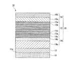
図1は、本実施形態のIII族窒化物半導体の製造方法を説明するための図であり、基板11上にIII族窒化物半導体が形成された積層半導体の一例を示す概略断面図である。図1に示す積層半導体10は、基板11上にIII族窒化物化合物からなるバッファ層12が積層され、該バッファ層12上に、n型半導体層14、発光層15、及びp型半導体層16が順次積層されてなる半導体層20が形成されている。
以下、本実施形態のIII族窒化物半導体の積層構造について詳述する。
<Semiconductor laminated structure>
FIG. 1 is a diagram for explaining the group III nitride semiconductor manufacturing method of the present embodiment, and is a schematic cross-sectional view showing an example of a stacked semiconductor in which a group III nitride semiconductor is formed on a
Hereinafter, the laminated structure of the group III nitride semiconductor of this embodiment will be described in detail.
『基板』
本実施形態では、基板11の材料としてサファイアを用いる。
本実施形態において、基板11に用いることができる材料としては、III族窒化物半導体結晶が表面にエピタキシャル成長される基板材料であれば、特に限定されず、各種材料を選択して用いることができ、例えば、サファイア、SiC、シリコン、酸化亜鉛、酸化マグネシウム、酸化マンガン、酸化ジルコニウム、酸化マンガン亜鉛鉄、酸化マグネシウムアルミニウム、ホウ化ジルコニウム、酸化ガリウム、酸化インジウム、酸化リチウムガリウム、酸化リチウムアルミニウム、酸化ネオジウムガリウム、酸化ランタンストロンチウムアルミニウムタンタル、酸化ストロンチウムチタン、酸化チタン、ハフニウム、タングステン、モリブデン等が挙げられる。この中でも、サファイア、SiC等の六方晶構造を有する材料を基板に用いることが、結晶性の良好なIII族窒化物半導体を積層できる点で好ましく、サファイアを用いることがより好ましい。また、基板の大きさとしては、通常は直径2インチ程度のものが用いられるが、本発明のIII族窒化物半導体では、直径4〜6インチの基板を使用することも可能である。
"substrate"
In this embodiment, sapphire is used as the material of the
In the present embodiment, the material that can be used for the
なお、アンモニアを使用せずにバッファ層を成膜するとともに、アンモニアを使用する方法で後述のn型半導体層を構成する下地層を成膜することにより、上記基板材料の内、高温でアンモニアに接触することで化学的な変性を引き起こすことが知られている酸化物基板や金属基板等を用いた場合には、本実施形態のバッファ層がコート層として作用するので、基板の化学的な変質を防ぐ点で効果的である。また、一般的に、スパッタ法は基板の温度を低く抑えることが可能なので、高温で分解してしまう性質を持つ材料からなる基板を用いた場合でも、基板11にダメージを与えることなく基板上への各層の成膜が可能である。
In addition, while forming a buffer layer without using ammonia, and forming a base layer constituting an n-type semiconductor layer described later by a method using ammonia, the substrate material is formed into ammonia at a high temperature. When an oxide substrate or a metal substrate that is known to cause chemical modification by contact is used, the buffer layer of this embodiment functions as a coating layer, so that chemical modification of the substrate is performed. It is effective in preventing. In general, since the sputtering method can keep the substrate temperature low, even when a substrate made of a material that decomposes at a high temperature is used, the
『バッファ層』
本実施形態の積層半導体10は、基板11上に、反応性スパッタ法により、金属原料とV族元素を含んだガスとがプラズマで活性化されて反応することで、III族窒化物化合物からなるバッファ層12が成膜されている。本実施形態のような、プラズマ化した金属原料を用いた方法で成膜された膜は、配向が得られ易いという作用がある。
"Buffer layer"
The
このようなバッファ層をなすIII族窒化物化合物の結晶は、六方晶系の結晶構造を持ち、成膜条件をコントロールすることにより、単結晶膜とすることができる。また、III族窒化物化合物の結晶は、上記成膜条件をコントロールすることにより、六角柱を基本とした集合組織からなる柱状結晶とすることも可能である。なお、ここで説明する柱状結晶とは、隣接する結晶粒との間に結晶粒界を形成して隔てられており、それ自体は縦断面形状として柱状になっている結晶のことをいう。 The group III nitride compound crystal forming such a buffer layer has a hexagonal crystal structure, and can be formed into a single crystal film by controlling the film formation conditions. Further, the group III nitride compound crystal can be formed into a columnar crystal having a texture based on a hexagonal column by controlling the film forming conditions. Note that the columnar crystal described here is a crystal that is separated by forming a crystal grain boundary between adjacent crystal grains, and itself has a columnar shape as a longitudinal sectional shape.
バッファ層12は、単結晶構造であることが、バッファ機能の面から好ましい。上述したように、III族窒化物化合物の結晶は、六方晶系の結晶を有し、六角柱を基本とした組織を形成する。III族窒化物化合物の結晶は、成膜等の条件を制御することにより、面内方向にも成長した結晶を成膜することが可能となる。このような単結晶構造を有するバッファ層12を基板11上に成膜した場合、バッファ層12のバッファ機能が有効に作用するため、その上に成膜されるIII族窒化物半導体の層は、良好な配向性及び結晶性を持つ結晶膜となる。
The
バッファ層12の膜厚は、20〜80nmの範囲とされていることが好ましい。バッファ層12の膜厚をこの範囲とすることにより、良好な配向性を有し、また、バッファ層12上にIII族窒化物半導体からなる各層を成膜する際に、コート層として有効に機能するバッファ層12が得られる。
バッファ層12の膜厚が20nm未満だと、上述したコート層としての機能が充分でなくなる虞がある。また、80nmを超える膜厚でバッファ層12を形成した場合、コート層としての機能には変化が無いのにも関わらず成膜処理時間が長くなり、生産性が低下する虞がある。
The thickness of the
If the thickness of the
バッファ層12は、Alを含有する組成とされていることが好ましい。バッファ層12を構成する材料としては、一般式AlGaInNで表されるIII族窒化物半導体であれば、どのような材料でも用いることができる。さらに、V族として、AsやPが含有される構成としても良い。また、バッファ層12を、Alを含んだ組成とした場合、中でも、GaAlNとすることが好ましく、この際、Alの組成が50%以上とされていることが好ましい。また、バッファ層12は、AlNからなる構成とすることがより好ましい。
It is preferable that the
また、バッファ層12を構成する材料としては、III族窒化物半導体と同じ結晶構造を有するものであれば、どのような材料でも用いることができるが、格子の長さが後述の下地層を構成するIII族窒化物半導体に近いものが好ましく、特に周期表のIIIa族元素の窒化物が好適である。
Any material can be used for the
『半導体層』
図1に示すように、本実施形態の積層半導体10は、基板11上に、上述のようなバッファ層12を介して、III族窒化物系半導体からなり、n型半導体層14、発光層15及びp型半導体層16から構成される半導体層20が積層されてなる。また、図示例の積層半導体10は、n型半導体層14に備えられた下地層14aがバッファ層12上に積層されている。
"Semiconductor layer"
As shown in FIG. 1, the
III族窒化物半導体としては、例えば、一般式AlXGaYInZN1−AMA(0≦X≦1、0≦Y≦1、0≦Z≦1で且つ、X+Y+Z=1。記号Mは窒素(N)とは別の第V族元素を表し、0≦A<1である。)で表わされる窒化ガリウム系化合物半導体が多数知られており、本発明においても、それら周知の窒化ガリウム系化合物半導体を含めて一般式AlXGaYInZN1−AMA(0≦X≦1、0≦Y≦1、0≦Z≦1で且つ、X+Y+Z=1。記号Mは窒素(N)とは別の第V族元素を表し、0≦A<1である。)で表わされる窒化ガリウム系化合物半導体を何ら制限なく用いることができる。 The group III nitride semiconductor, for example, and by the general formula Al X Ga Y In Z N 1 -A M A (0 ≦ X ≦ 1,0 ≦ Y ≦ 1,0 ≦ Z ≦ 1, X + Y + Z = 1. Symbol M represents a group V element different from nitrogen (N), and 0 ≦ A <1.) Many gallium nitride-based compound semiconductors are known. and the general formula Al X Ga Y in Z N 1 -a M a (0 ≦ X ≦ 1,0 ≦ Y ≦ 1,0 ≦ Z ≦ 1 , including the gallium compound semiconductor, X + Y + Z = 1 . symbol M nitrogen A gallium nitride-based compound semiconductor represented by (V) represents another group V element and 0 ≦ A <1) can be used without any limitation.
窒化ガリウム系化合物半導体は、Al、GaおよびIn以外に他のIII族元素を含有することができ、必要に応じてGe、Si、Mg、Ca、Zn、Be、P及びAs等の元素を含有することもできる。さらに、意図的に添加した元素に限らず、成膜条件等に依存して必然的に含まれる不純物、並びに原料、反応管材質に含まれる微量不純物を含む場合もある。 Gallium nitride compound semiconductors can contain other group III elements in addition to Al, Ga, and In, and contain elements such as Ge, Si, Mg, Ca, Zn, Be, P, and As as necessary. You can also Furthermore, it is not limited to the element added intentionally, but may include impurities that are inevitably included depending on the film forming conditions and the like, as well as trace impurities that are included in the raw materials and reaction tube materials.
「n型半導体層」
n型半導体層14は、通常、前記バッファ層12上に積層され、下地層14a、n型コンタクト層14b及びn型クラッド層14cから構成される。なお、n型コンタクト層は、下地層、及び/又は、n型クラッド層を兼ねることが可能であるが、下地層が、n型コンタクト層、及び、n型クラッド層を兼ねることも可能である。
"N-type semiconductor layer"
The n-
{下地層}
本実施形態の下地層14aはIII族窒化物半導体からなり、反応性スパッタ法でバッファ層12上に積層して成膜される。
下地層14aの材料としては、必ずしも基板11上に成膜されたバッファ層12と同じである必要はなく、異なる材料を用いても構わないが、AlyGa1―yN層(0≦y≦1、好ましくは0≦y≦0.5、さらに好ましくは0≦y≦0.1)から構成されることが好ましい。
{Underlayer}
The
The material of the
本発明では、バッファ層12上に、単結晶のIII族窒化物半導体からなる下地層14aを予め形成する。単結晶の下地層14aの上には、結晶性の良好なIII族窒化物半導体の単結晶層を容易にスパッタ法により形成することができるため、ドーパントを添加して導電性を制御したIII族窒化物半導体が得られやすくなる。
In the present invention, a
下地層14aに用いる材料としては、Gaを含むIII族窒化物化合物、即ちGaN系化合物半導体が用いられ、特に、AlGaN、又はGaNを好適に用いることができる。また、バッファ層12を、例えば、AlNからなる柱状結晶の集合体として形成した場合には、下地層14aがバッファ層12の結晶性をそのまま引き継がないように、マイグレーションによって転位をループ化させる必要があるが、このような材料としても上記Gaを含むGaN系化合物半導体が挙げられ、特に、AlGaN、又はGaNが好適である。
As a material used for the
下地層14aの膜厚は、0.1〜8μmの範囲とすることが、結晶性の良好な下地層が得られる点で好ましく、0.1〜2μmの範囲とすることが、成膜に要する工程時間を短縮でき、生産性が向上する点でより好ましい。
The film thickness of the
下地層14aは、必要に応じて、ドナー不純物(n型不純物)が1×10¹⁷〜1×10¹⁹/cm3の範囲内でドープされた構成としても良いが、アンドープ(<1×1017/cm3)の構成とすることもでき、アンドープとした場合には、良好な結晶性を維持できる点で好ましい。基板11が導電性である場合には、下地層14aにドーパントをドープして導電性とすることにより、発光素子の上下に電極を形成することができる。一方、基板11に絶縁性の材料を用いる場合には、発光素子の同じ面に正極及び負極の各電極が設けられたチップ構造をとることになるので、基板11直上の層はドープしない結晶とした方が、結晶性が良好となるので好ましい。n型不純物としては、特に限定されないが、例えば、Si、GeおよびSn等が挙げられ、好ましくはSiおよびGeが挙げられる。
The
{n型コンタクト層}
本実施形態のn型コンタクト層14bはIII族窒化物半導体からなり、反応性スパッタ法で下地層14a上に積層して成膜される。
n型コンタクト層14bとしては、下地層14aと同様にAlXGa1―XN層(0≦x≦1、好ましくは0≦x≦0.5、さらに好ましくは0≦x≦0.1)から構成されることが好ましい。また、n型不純物がドープされていることが好ましく、n型不純物を1×10¹⁷〜1×10¹⁹/cm3、好ましくは1×1018〜1×1019/cm3の濃度で含有すると、負極との良好なオーミック接触の維持、クラック発生の抑制、良好な結晶性の維持の点で好ましい。n型不純物としては、特に限定されないが、例えば、Si、GeおよびSn等が挙げられ、好ましくはSiおよびGeである。成長温度は下地層と同様である。また、上述したように、n型コンタクト層14bは、下地層を兼ねた構成とすることもできる。
{N-type contact layer}
The n-
As the n-
下地層14a及びn型コンタクト層14bを構成する窒化ガリウム系化合物半導体は同一組成であることが好ましく、これらの合計の膜厚を0.1〜20μm、好ましくは0.5〜15μm、さらに好ましくは1〜12μmの範囲に設定することが好ましい。膜厚がこの範囲であると、半導体の結晶性が良好に維持される。
The gallium nitride-based compound semiconductor constituting the
{n型クラッド層}
上述のn型コンタクト層14bと詳細を後述する発光層15との間には、n型クラッド層14cを設けることが好ましい。n型クラッド層14cを設けることにより、n型コンタクト層14bの最表面に生じた平坦性の悪化を改善することができる。n型クラッド層14cは、従来公知のMOCVD法を用いて、AlGaN、GaN、GaInN等により成膜することが可能である。また、これらの構造のヘテロ接合や複数回積層した超格子構造としてもよい。GaInNとする場合には、発光層15のGaInNのバンドギャップよりも大きくすることが望ましいことは言うまでもない。
{N-type cladding layer}
It is preferable to provide an n-
n型クラッド層14cの膜厚は、特に限定されないが、好ましくは5〜500nmの範囲であり、より好ましくは5〜100nmの範囲である。
また、n型クラッド層14cにおけるn型不純物のドープ濃度は1×10¹⁷〜1×10²⁰/cm3の範囲とされていることが好ましく、より好ましくは1×1018〜1×1019/cm3の範囲である。ドープ濃度がこの範囲であると、良好な結晶性の維持および発光素子の動作電圧低減の点で好ましい。
The film thickness of the n-
The n-type impurity doping concentration in the n-
なお、n型クラッド層14cを、超格子構造を含む層とする場合には、詳細な図示を省略するが、100オングストローム以下の膜厚を有したIII族窒化物半導体からなるn側第1層と、該n側第1層と組成が異なるとともに100オングストローム以下の膜厚を有したIII族窒化物半導体からなるn側第2層とが積層された構造を含むものであっても良い。また、n型クラッド層14cは、n側第1層とn側第2層とが交互に繰返し積層された構造を含んだものであってもよい。
When the n-
上述のようなn側第1層及びn側第2層は、例えばAlを含むAlGaN系(以下、単にAlGaNと記載することがある)、Inを含むGaInN系(以下、単にGaInNと記載することがある)、GaNの組成とすることができる。また、n側第1層及びn側第2層は、GaInN/GaNの交互構造、AlGaN/GaNの交互構造、GaInN/AlGaNの交互構造、組成の異なるGaInN/GaInNの交互構造、組成の異なるAlGaN/AlGaNの交互構造であってもよい。本発明においては、n側第1層及びn側第2層は、GaInN/GaNの交互構造又は組成の異なるGaInN/GaInNであることが好ましい。 The n-side first layer and the n-side second layer as described above are, for example, AlGaN-based Al (hereinafter, simply referred to as AlGaN), GaInN-based (hereinafter simply referred to as GaInN) including In. The composition of GaN. In addition, the n-side first layer and the n-side second layer are composed of an alternate structure of GaInN / GaN, an alternate structure of AlGaN / GaN, an alternate structure of GaInN / AlGaN, an alternate structure of GaInN / GaInN having different compositions, and an AlGaN having different compositions. / AlGaN alternate structure may be used. In the present invention, the n-side first layer and the n-side second layer are preferably GaInN / GaInN having different GaInN / GaN structures or different compositions.
上記n側第1層及びn側第2層の超格子層は、それぞれ60オングストローム以下であることが好ましく、それぞれ40オングストローム以下であることがより好ましく、それぞれ10オンストローム〜40オングストロームの範囲であることが最も好ましい。超格子層を形成するn側第1層とn側第2層の膜厚が100オングストローム超だと、結晶欠陥が入りやすく好ましくない。 The superlattice layers of the n-side first layer and the n-side second layer are each preferably 60 angstroms or less, more preferably 40 angstroms or less, and each in the range of 10 angstroms to 40 angstroms. Most preferred. If the thicknesses of the n-side first layer and the n-side second layer forming the superlattice layer are more than 100 angstroms, crystal defects are likely to occur, which is not preferable.
上記n側第1層及びn側第2層は、それぞれドープした構造であってもよく、また、ドープ構造/未ドープ構造の組み合わせであってもよい。ドープされる不純物としては、上記材料組成に対して従来公知のものを、何ら制限無く適用できる。例えば、n型クラッド層として、GaInN/GaNの交互構造又は組成の異なるGaInN/GaInNの交互構造のものを用いた場合には、不純物としてSiが好適である。また、上述のようなn側超格子多層膜は、GaInNやGaAlN、GaNで代表される組成が同じであっても、ドーピングを適宜ON、OFFしながら作製してもよい。 The n-side first layer and the n-side second layer may each have a doped structure, or a combination of a doped structure and an undoped structure. As the impurity to be doped, conventionally known impurities can be applied to the material composition without any limitation. For example, when an n-type cladding layer having a GaInN / GaN alternating structure or a GaInN / GaInN alternating structure having a different composition is used, Si is suitable as an impurity. In addition, the n-side superlattice multilayer film as described above may be manufactured while doping is appropriately turned ON / OFF even if the composition represented by GaInN, GaAlN, and GaN is the same.
「発光層」
発光層15は、n型半導体層14上に積層されるとともに、詳細を後述するp型半導体層16がその上に積層される層であり、従来公知のMOCVD法等を用いて成膜することができる。また、発光層15は、図1に示すように、窒化ガリウム系化合物半導体からなる障壁層15aと、インジウムを含有する窒化ガリウム系化合物半導体からなる井戸層15bとが交互に繰り返して積層されてなり、図示例では、n型半導体層14側及びp型半導体層16側に障壁層15aが配される順で積層して形成されている。
"Light emitting layer"
The
障壁層15aとしては、例えば、インジウムを含有した窒化ガリウム系化合物半導体からなる井戸層15bよりもバンドギャップエネルギーが大きいAlcGa1−cN(0≦c<0.3)等の窒化ガリウム系化合物半導体を、好適に用いることができる。
また、井戸層15bには、インジウムを含有する窒化ガリウム系化合物半導体として、例えば、Ga1−sInsN(0<s<0.4)等の窒化ガリウムインジウムを用いることができる。
As the
Furthermore, the
また、発光層15全体の膜厚としては、特に限定されない。例えば、発光層15の膜厚は、1〜500nmの範囲であることが好ましく、100nm以下の膜厚であればより好ましい。膜厚が上記範囲であると、発光出力の向上に寄与する。
Further, the film thickness of the entire
「p型半導体層」
p型半導体層16は、通常、p型クラッド層16a及びp型コンタクト層16bから構成され、反応性スパッタ法を用いて発光層15上に成膜される。また、p型コンタクト層がp型クラッド層を兼ねる構成とすることもできる。
"P-type semiconductor layer"
The p-
本実施形態のp型半導体層16は、導電性をp型に制御するためのドーパントとして、アクセプター不純物が添加されてなる。アクセプター不純物としては、特に限定されないが、例えば、Mgを用いることが好ましく、また、同様にBeやZnを用いることも可能である。
The p-
{p型クラッド層}
p型クラッド層16aとしては、発光層15のバンドギャップエネルギーより大きくなる組成であり、発光層15へのキャリアの閉じ込めができるものであれば特に限定されないが、好ましくは、AldGa1−dN(0<d≦0.4、好ましくは0.1≦d≦0.3)のものが挙げられる。p型クラッド層16aが、このようなAlGaNからなると、発光層15へのキャリアの閉じ込めの点で好ましい。
p型クラッド層16aの膜厚は、特に限定されないが、好ましくは1〜400nmであり、より好ましくは5〜100nmである。
{P-type cladding layer}
The p-
The thickness of the p-
p型クラッド層16aにアクセプター不純物を添加することによって得られるp型ドープ濃度が、1×10¹⁸〜1×10²¹/cm3の範囲とされていることが好ましく、より好ましくは1×1019〜1×1020/cm3である。p型ドープ濃度が上記範囲であると、結晶性を低下させることなく良好なp型結晶が得られる。
The p-type dope concentration obtained by adding an acceptor impurity to the p-
なお、p型クラッド層16aは、複数回積層した超格子構造としてもよい。
p型クラッド層16aを、超格子構造を含む層とする場合には、詳細な図示を省略するが、100オングストローム以下の膜厚を有したIII族窒化物半導体からなるp側第1層と、該p側第1層と組成が異なるとともに100オングストローム以下の膜厚を有したIII族窒化物半導体からなるp側第2層とが積層された構造を含むものであっても良い。また、p側第1層とp側第2層とが交互に繰返し積層された構造を含んだものであっても良い。
Note that the p-
When the p-
上述のようなp側第1層及びp側第2層は、それぞれ異なる組成、例えば、AlGaN、GaInN又はGaNの内の何れの組成であっても良い、また、GaInN/GaNの交互構造、AlGaN/GaNの交互構造、又はGaInN/AlGaNの交互構造であっても良い。本発明においては、p側第1層及びp側第2層は、AlGaN/AlGaN又はAlGaN/GaNの交互構造であることが好ましい。 The p-side first layer and the p-side second layer as described above may have different compositions, for example, any composition of AlGaN, GaInN, or GaN. Alternatively, the GaInN / GaN alternating structure, AlGaN. An alternating structure of / GaN or an alternating structure of GaInN / AlGaN may be used. In the present invention, the p-side first layer and the p-side second layer preferably have an AlGaN / AlGaN or AlGaN / GaN alternating structure.
上記p側第1層及びp側第2層の超格子層は、それぞれ60オングストローム以下であることが好ましく、それぞれ40オングストローム以下であることがより好ましく、それぞれ10オングストローム〜40オングストロームの範囲であることが最も好ましい。超格子層を形成するp側第1層とp側第2層の膜厚が100オングストローム超だと、結晶欠陥等を多く含む層となり、好ましくない。 Each of the superlattice layers of the p-side first layer and the p-side second layer is preferably 60 angstroms or less, more preferably 40 angstroms or less, and each in the range of 10 angstroms to 40 angstroms. Is most preferred. If the thickness of the p-side first layer and the p-side second layer forming the superlattice layer exceeds 100 angstroms, it becomes a layer containing many crystal defects and the like, which is not preferable.
上記p側第1層及びp側第2層は、それぞれドープした構造であっても良く、また、ドープ構造/未ドープ構造の組み合わせであっても良い。ドープされる不純物としては、上記材料組成に対して従来公知のものを、何ら制限無く適用できる。例えば、p型クラッド層として、AlGaN/GaNの交互構造又は組成の異なるAlGaN/AlGaNの交互構造のものを用いた場合には、不純物としてMgが好適である。また、上述のようなp側超格子多層膜は、GaInNやAlGaN、GaNで代表される組成が同じであっても、ドーピングを適宜ON、OFFしながら作製してもよい。 The p-side first layer and the p-side second layer may each have a doped structure, or a combination of a doped structure and an undoped structure. As the impurity to be doped, conventionally known impurities can be applied to the material composition without any limitation. For example, when a p-type cladding layer having an AlGaN / GaN alternating structure or an AlGaN / AlGaN alternating structure having a different composition is used, Mg is suitable as an impurity. Further, the p-side superlattice multilayer film as described above may be manufactured while doping is appropriately turned on and off even if the composition represented by GaInN, AlGaN, and GaN is the same.
{p型コンタクト層}
p型コンタクト層16bとしては、少なくともAleGa1−eN(0≦e<0.5、好ましくは0≦e≦0.2、より好ましくは0≦e≦0.1)を含んでなる窒化ガリウム系化合物半導体層である。Al組成が上記範囲であると、良好な結晶性の維持およびpオーミック電極(後述の透光性電極17を参照)との良好なオーミック接触の点で好ましい。
p型コンタクト層16bの膜厚は、特に限定されないが、10〜500nmが好ましく、より好ましくは50〜200nmである。膜厚がこの範囲であると、発光出力の点で好ましい。
{P-type contact layer}
The p-
Although the film thickness of the p-
また、p型コンタクト層16bにアクセプター不純物を添加することによって得られるp型ドープ濃度が、1×10¹⁸〜1×10²¹/cm3の範囲とされていると、良好なオーミック接触の維持、クラック発生の防止、良好な結晶性の維持の点で好ましく、より好ましくは5×1019〜5×1020/cm3の範囲である。
Further, when the p-type dope concentration obtained by adding the acceptor impurity to the p-
<製造方法>
本実施形態のIII族窒化物半導体の製造方法は、上述したように、チャンバ41内に基板11及びGa元素を含有するターゲット47を配置するとともに、反応ガス供給手段50によってチャンバ41内に窒素原子含有ガス及び不活性ガスを供給し、基板11上に単結晶のIII族窒化物半導体をプラズマによる反応性スパッタ法で形成する方法であり、チャンバ41内の圧力を圧力モニタ51で検知し、該圧力モニタ51の検知信号Aに基づき、反応ガス供給手段50からチャンバ41内に供給する窒素原子含有ガスの流通量を流量制御手段52によって制御する方法である。
<Manufacturing method>
In the method for producing a group III nitride semiconductor according to the present embodiment, as described above, the
本実施形態の製造方法では、基板11上にIII族窒化物半導体結晶をエピタキシャル成長させ、図1に示すような積層半導体10を形成する際、基板11上にバッファ層12を成膜し、その上に半導体層20を形成する。本実施形態では、バッファ層12を反応性スパッタ法で形成し、その上に、n型半導体層14の下地層14a及びn型コンタクト層14bを反応性スパッタ法で形成した後、n型クラッド層14を従来公知のMOCVD法で形成し、その上に、発光層15従来公知のMOCVD法で形成し、さらにその上に、p型半導体層16を構成するp型クラッド層16a及びp型コンタクト層16bの各層を反応性スパッタ法で形成する方法としている。
そして、本実施形態においては、半導体層20を構成するn型半導体層14及びp型半導体層16の内、下地層14a、n型コンタクト層14b、p型クラッド層16a及びp型コンタクト層16bの各層を、上記方法によって窒素原子含有ガスの流通量を制御しながら反応性スパッタ法によって成膜する。
In the manufacturing method of this embodiment, when a group III nitride semiconductor crystal is epitaxially grown on the
In this embodiment, among the n-
『スパッタ装置(III族窒化物半導体製造装置)』
以下に、本実施形態の製造方法で用いられ、下地層14a、n型コンタクト層14b、p型クラッド層16a及びp型コンタクト層16bの各層を成膜するためのスパッタ装置の構成について、図5に例示するようなRF放電式のスパッタ装置40を用いて詳述する。
図5に例示するスパッタ装置40(III族窒化物半導体製造装置)は、チャンバ41にGa元素を含有してなるターゲット47が電極43上に配置されており、電極43の下方(図5の下方)にマグネット42が配され、該マグネット42が図示略の駆動装置によってターゲット47の下方で揺動する。チャンバ41には窒素ガス及びアルゴンガスが供給され、ヒータプレート44に取り付けられた基板11上に各層が成膜される。
また、スパッタ装置40には、チャンバ41内に窒素原子含有ガス及び不活性ガスを供給するための反応ガス供給手段50が備えられているとともに、チャンバ41内の圧力を検知する圧力モニタ51が設けられている。そして、スパッタ装置40には、圧力モニタ51の検知信号Aに基づき、反応ガス供給手段50からチャンバ41内に供給する窒素原子含有ガスの流通量を制御するための流量制御手段52が設けられている。
"Sputtering equipment (Group III nitride semiconductor manufacturing equipment)"
Hereinafter, the configuration of a sputtering apparatus used in the manufacturing method of the present embodiment for forming each layer of the
In a sputtering apparatus 40 (group III nitride semiconductor manufacturing apparatus) illustrated in FIG. 5, a
Further, the
電極43はマッチングボックス46に接続されており、また、ヒータプレート44には基板11が取り付けられるとともにマッチングボックス45が接続されている。このようなマッチングボックス46及び45は、各々、電源48に接続されており、電極43にはマッチングボックス46を介して電流が供給され、ヒータプレート44にはマッチングボックス45を介して電流が供給される。これにより、ターゲット47にはパワーが印加され、基板11にはバイアスが印加される。上述のマッチングボックス46及び45は、スパッタ装置40内部と、高周波の電源48とのインピーダンスのマッチングをとるために設けられる。
The
本実施形態の製造方法で用いるスパッタ装置としては、RFスパッタ法によって成膜処理を行う装置であることが好ましい。III族窒化物半導体からなる半導体層をスパッタ法で成膜する場合、一般に、III族金属をターゲットにし、スパッタ装置のチャンバ内に窒素原子含有ガス(窒素ガス:N2、アンモニア:NH3等)を導入し、気相中でIII族金属と窒素を反応させる反応性スパッタ法(リアクティブスパッタ法)を用いる。スパッタ法としては、RFスパッタ及びDCスパッタがあるが、本発明の製造方法のように反応性スパッタ法を用いた場合には、連続的に放電させるDCスパッタでは帯電が激しく、成膜速度のコントロールが困難となる。このため、本発明の製造方法では、RFスパッタ法を用いることが好ましく、DCスパッタ法を用いる場合には、パルス的にバイアスを与えることができるパルスDCスパッタ法が採用されたスパッタ装置を用いることが好ましい。 The sputtering apparatus used in the manufacturing method of this embodiment is preferably an apparatus that performs a film forming process by an RF sputtering method. When a semiconductor layer made of a group III nitride semiconductor is formed by sputtering, generally a group III metal is used as a target, and a nitrogen atom-containing gas (nitrogen gas: N 2 , ammonia: NH 3 or the like) is placed in the chamber of the sputtering apparatus. And a reactive sputtering method (reactive sputtering method) in which a group III metal and nitrogen are reacted in a gas phase. As sputtering methods, there are RF sputtering and DC sputtering. When reactive sputtering is used as in the manufacturing method of the present invention, DC sputtering with continuous discharge is intensely charged, and film formation speed is controlled. It becomes difficult. For this reason, in the manufacturing method of the present invention, it is preferable to use the RF sputtering method, and when using the DC sputtering method, use a sputtering apparatus employing a pulsed DC sputtering method capable of applying a bias in a pulsed manner. Is preferred.
また、RFスパッタを用いた場合には、帯電を回避する方法として、マグネットの位置をターゲット内で移動させることが好ましい。具体的な運動の方法は、使用するスパッタ装置によって選択することができ、揺動させたり、回転運動させたりすることができる。 図5に例示するスパッタ装置40では、ターゲット47の下方にマグネット42が備えられ、このマグネット42がターゲット47の下方で回転運動できる構成とされている。
When RF sputtering is used, it is preferable to move the position of the magnet within the target as a method for avoiding charging. A specific motion method can be selected depending on a sputtering apparatus to be used, and can be swung or rotated. In the
また、チャンバ41内には、できるだけ不純物を残さないことが好ましいので、スパッタ装置40の到達真空度は、少なくとも1.0×10⁻³Pa以下であることが好ましい。
In addition, since it is preferable to leave as little impurities as possible in the
また、詳細な図示を省略するが、スパッタ装置40のチャンバ41内にドーパント供給手段を配置することにより、III族窒化物半導体にドナー不純物やアクセプター不純物等のドーパントを添加して各層を成膜することができる。また、ターゲットに予めドーパントを混合して成膜処理を行なうこともでき、その他、チャンバの外部からチャンバ内へ向けてドーパントを供給する構成とすることも可能である。
Although not shown in detail, the dopant supply means is disposed in the
本実施形態で用いるスパッタ装置40には、上述したように、チャンバ41内に窒素原子含有ガス及び不活性ガスを供給するための反応ガス供給手段50と、チャンバ41内の圧力を検知する圧力モニタ51と、圧力モニタ51の検知信号Aに基づき、反応ガス供給手段50からチャンバ41内に供給する窒素原子含有ガスの流通量を制御するための流量制御手段52とが設けられている。
In the
反応ガス供給手段50は、チャンバ41内に窒素原子含有ガス(N2)及び不活性ガス(Ar)の各反応ガスを、適宜供給量を調整して供給するものであり、図5に示す例では、配管53a、53bを介してチャンバ41に各反応ガスを供給できるように構成されている。また、図示例では、配管53aが窒素原子含有ガスの供給管とされ、配管53bが不活性ガスの供給管とされている。
The reactive gas supply means 50 supplies each reactive gas of nitrogen atom-containing gas (N 2 ) and inert gas (Ar) into the
圧力モニタ51は、チャンバ41内の圧力を検知して検知信号Aとし、該検知信号Aを、詳細を後述する窒素流量制御手段に送信する検出手段である。圧力モニタ51は、チャンバ41内の圧力を検知することにより、チャンバ41内の圧力と相関する窒素原子量を検出することができる。
なお、図示例の圧力モニタ51は、チャンバ41の外壁に接続するように配置されているが、これには限定されず、例えば、チャンバ41内に配置することも可能であり、適宜決定することが可能である。
The pressure monitor 51 is a detection unit that detects the pressure in the
The pressure monitor 51 in the illustrated example is arranged so as to be connected to the outer wall of the
窒素流量制御手段52は、圧力モニタ51から送信される検知信号Aに基づき、内部に備えられる図示略の電磁バルブや制御回路等の手段によって窒素原子含有ガスの流量を制御するものであり、例えば、従来公知のマスフローコントローラ等を何ら制限無く用いることができる。また、窒素流量制御手段52は、図示例では、反応ガス供給手段50からチャンバ41内に向けて窒素原子含有ガスが供給される配管53aの経路に設けられている。
The nitrogen flow rate control means 52 controls the flow rate of the nitrogen atom-containing gas by means such as an electromagnetic valve or a control circuit (not shown) provided inside based on the detection signal A transmitted from the
本実施形態のスパッタ装置40は、チャンバ41内と圧力モニタ51との間を、詳細な図示を省略する配管等で接続し、チャンバ41内の圧力を圧力モニタ51で検知することにより、後述の動作形態において説明するように、圧力モニタ51を、チャンバ41内の窒素原子量検出手段として用いた構成としている。
The
上述のように、圧力モニタ51が窒素流量検出手段として用いられてなるスパッタ装置40の動作について、以下に説明する。
例えば、スパッタ装置40を用いてIII族窒化物半導体の成膜を繰り返した際、チャンバ41の内壁や図示略のシールド部材に窒素原子を含むデポジションが付着する。その後、さらにIII族窒化物半導体の成膜を繰り返すことにより、チャンバ41内のデポジションが分解して窒素を発生するので、チャンバ41内の活性な窒素量が増大し、チャンバ41内の圧力が上昇する。この際、圧力モニタ51がチャンバ41内の圧力を検知し、その圧力に応じて検知信号Aを窒素流量制御手段52に向けて出力する。そして、窒素流量制御手段52は、内部に備えられる図示略の制御回路において上記検知信号Aに基づいて判定を行ない、検知信号Aが予め設定された閾値よりも大きなチャンバ内圧力を示す信号であった場合には、図示略の電磁バルブを閉動作させて窒素原子含有ガスのチャンバ41内への供給を減少させる。これにより、チャンバ41内の窒素の量は、過多な状態から徐々に減少してゆき、これと同時に、チャンバ41内の圧力も徐々に低下してゆく。そして、圧力モニタから窒素流量制御手段52に向けて出力される検知信号Aが、予め設定された閾値より小さいか、あるいは閾値と同じチャンバ内圧力を示す信号となった場合には、図示略の電磁バルブの開動作を行い、窒素原子含有ガスのチャンバ41内への供給量を増加させる。
このように、チャンバ41内の圧力が一定となるような制御を行なうことにより、チャンバ41内の活性な窒素の量も一定に制御することが可能となる。また、本実施形態のスパッタ装置40は、圧力モニタ51がチャンバ41内の窒素原子量検出手段として採用された構成なので、装置が簡便であるとともに、窒素量を正確に検出することが可能となる。
As described above, the operation of the
For example, when the film formation of the group III nitride semiconductor is repeated using the
As described above, by controlling the pressure in the
本実施形態のスパッタ装置40は、上記構成により、チャンバ41内の圧力を圧力モニタ51で検知することでチャンバ41内に存在する活性な窒素の量を検出し、その検出結果をフィードバックして窒素原子含有ガスの流量制御を行なうことにより、チャンバ41内における活性窒素量を一定とし、常に同一のスパッタ条件を得ることができる。これにより、チャンバ41内におけるGaと窒素との比率を安定させ、結晶性に優れるGaN結晶の層を、高効率で安定して基板上に成膜することが可能となる。
With the above configuration, the
なお、チャンバ41内の活性な窒素の量を検出するための方法としては、本実施形態のような圧力検知による方法の他、例えば、質量分析装置等を用いて窒素量を検出する方法があり、適宜採用することができる。
As a method for detecting the amount of active nitrogen in the
『積層半導体の形成』
本実施形態の製造方法を用いて、図1に示すような積層半導体10を形成する際の各層の成膜方法について以下に詳述する。
“Formation of laminated semiconductors”
A method for forming each layer when forming the
「バッファ層の形成」
本実施形態の製造方法では、基板11上に反応性スパッタ法によってバッファ層12を形成することが好ましい。
また、基板11を反応器(スパッタ装置)の中に導入した後、バッファ層12を形成する前に、スパッタ法等の方法を用いて前処理を行うことが好ましい。このような前処理は、具体的には、基板11をArやN2のプラズマ中に曝す事によって表面を整えることができる処理である。例えば、ArガスやN2ガスなどのプラズマを基板11表面に作用させることで、基板11表面に付着した有機物や酸化物を除去することができる。この場合、基板11とチャンバとの間に電圧を印加すれば、プラズマ粒子が効率的に基板11に作用する。このような前処理を基板11に施すことにより、基板11の表面11a全面にバッファ層12を成膜することができ、その上に成膜される膜の結晶性を高めることが可能となる。また、バッファ層12を基板11上に成膜する際、基板11には湿式の前処理を行っても良い。
"Formation of buffer layer"
In the manufacturing method of this embodiment, it is preferable to form the
In addition, after introducing the
本実施形態では、上述した前処理を、イオン成分と、電荷を持たないラジカル成分とが混合された雰囲気で行なわれるプラズマ処理により、基板11の表面を処理する方法を用いた工程としている。
ここで、基板の表面からコンタミ等を除去する際、例えば、イオン成分等を単独で基板表面に供給した場合には、エネルギーが強すぎて基板表面にダメージを与えてしまい、基板上に成長させる結晶の品質を低下させてしまうという問題がある。
本実施形態の前処理においては、上述のように、イオン成分とラジカル成分とが混合された雰囲気で行なわれるプラズマ処理を用いた方法とし、基板11に適度なエネルギーを持つ反応種を作用させることにより、基板11表面にダメージを与えずにコンタミ等の除去を行なうことが可能となる。このような効果が得られるメカニズムとしては、イオン成分の割合が少ないプラズマを用いることで基板表面に与えるダメージが抑制されることと、基板表面にプラズマを作用させることによって効果的にコンタミを除去できること等が考えられる。
In the present embodiment, the pretreatment described above is a process using a method of treating the surface of the
Here, when removing contaminants and the like from the surface of the substrate, for example, when an ionic component or the like is supplied to the substrate surface alone, the energy is too strong and the substrate surface is damaged and grown on the substrate. There is a problem that the quality of the crystal is lowered.
In the pretreatment of this embodiment, as described above, a method using plasma treatment performed in an atmosphere in which an ionic component and a radical component are mixed is used, and a reactive species having appropriate energy is allowed to act on the
上記方法で基板11表面の前処理を行なった後、スパッタ装置内にアルゴン及び窒素ガスを導入し、基板11の温度を500℃程度にする。そして、基板11側に高周波バイアスを印加するとともに、金属AlからなるAlターゲット側にパワーを印加し、炉内の圧力を一定に保ちながら、基板11上にAlNからなるバッファ層12を成膜する。
After pretreatment of the surface of the
バッファ層12を基板11上に成膜する方法としては、スパッタ法の他、例えば、MOCVD法、パルスレーザーデポジション(PLD)法、パルス電子線堆積(PED)法等が挙げられ、適宜選択して用いることができるが、スパッタ法が最も簡便で量産にも適しているため、好適な方法である。なお、DCスパッタを用いる場合、ターゲット表面のチャージアップを招き、成膜速度が安定しない可能性があるので、パルスDCスパッタ法とするか、RFスパッタ法とすることが望ましい。また、バッファ層12の成膜処理には、ターゲットや各成膜条件を変更することにより、上述のようなスパッタ装置40を用いることも可能である。
Examples of the method for forming the
「半導体層の形成」
バッファ層12上には、n型半導体層14、発光層15、p型半導体層16をこの順で積層することにより、III族窒化物半導体からなる半導体層20を形成する。本実施形態の製造方法では、上述したように、n型半導体層14の下地層14a及びn型コンタクト層14bを反応性スパッタ法によって形成した後、n型クラッド層14c及びその上の発光層をMOCVD法で形成し、そして、p型半導体層16を構成するp型クラッド層16a及びp型コンタクト層16bの各層を反応性スパッタ法で形成する。
"Semiconductor layer formation"
On the
MOCVD法では、キャリアガスとして水素(H2)または窒素(N2)、III族原料であるGa源としてトリメチルガリウム(TMG)またはトリエチルガリウム(TEG)、Al源としてトリメチルアルミニウム(TMA)またはトリエチルアルミニウム(TEA)、In源としてトリメチルインジウム(TMI)またはトリエチルインジウム(TEI)、V族原料であるN源としてアンモニア(NH3)、ヒドラジン(N2H4)などが用いられる。また、ドーパントとしては、n型にはSi原料としてモノシラン(SiH4)またはジシラン(Si2H6)を、Ge原料としてゲルマンガス(GeH4)や、テトラメチルゲルマニウム((CH3)4Ge)やテトラエチルゲルマニウム((C2H5)4Ge)等の有機ゲルマニウム化合物を利用できる。MBE法では、元素状のゲルマニウムもドーピング源として利用できる。p型にはMg原料としては、例えばビスシクロペンタジエニルマグネシウム(Cp2Mg)またはビスエチルシクロペンタジエニルマグネシウム(EtCp2Mg)を用いる。 In the MOCVD method, hydrogen (H 2 ) or nitrogen (N 2 ) as a carrier gas, trimethyl gallium (TMG) or triethyl gallium (TEG) as a Ga source which is a group III source, trimethyl aluminum (TMA) or triethyl aluminum as an Al source (TEA), trimethylindium (TMI) or triethylindium (TEI) as an In source, ammonia (NH 3 ), hydrazine (N 2 H 4 ), or the like as an N source as a group V source. In addition, as a dopant, for n-type, monosilane (SiH 4 ) or disilane (Si 2 H 6 ) is used as a Si raw material, germanium gas (GeH 4 ) or tetramethyl germanium ((CH 3 ) 4 Ge) is used as a Ge raw material. And organic germanium compounds such as tetraethylgermanium ((C 2 H 5 ) 4 Ge) can be used. In the MBE method, elemental germanium can also be used as a doping source. For the p-type, for example, biscyclopentadienyl magnesium (Cp 2 Mg) or bisethylcyclopentadienyl magnesium (EtCp 2 Mg) is used as the Mg raw material.
上述したような窒化ガリウム系化合物半導体は、Al、GaおよびIn以外に他のIII族元素を含有することができ、必要に応じてGe、Si、Mg、Ca、Zn、Be等のドーパント元素を含有することができる。さらに、意図的に添加した元素に限らず、成膜条件等に依存して必然的に含まれる不純物、並びに原料、反応管材質に含まれる微量不純物を含む場合もある。 The gallium nitride-based compound semiconductor as described above can contain other group III elements in addition to Al, Ga, and In. If necessary, dopant elements such as Ge, Si, Mg, Ca, Zn, and Be can be added. Can be contained. Furthermore, it is not limited to the element added intentionally, but may include impurities that are inevitably included depending on the film forming conditions and the like, as well as trace impurities that are included in the raw materials and reaction tube materials.
そして、上述のようなスパッタ装置40を用いて、反応性スパッタ法で基板11上に半導体層を成膜する際は、まず、チャンバ41内に、例えば、アルゴンガス及び窒素ガス等の反応ガスを供給し、ヒータプレート44内に設けられた図示略の加熱手段によってヒータプレート44を発熱させ、基板11を所定の温度、つまり、基板11上に成長させられる各層の成長温度に加温し、各層の成膜処理を行なう。
When a semiconductor layer is formed on the
{反応性スパッタ成膜条件}
本実施形態では、半導体層20の各層の内、下地層14a、n型コンタクト層14b、p型クラッド層16a及びp型コンタクト層16bの各層を、反応性スパッタ法を用いて成膜する。このように、反応性スパッタ法を用いて半導体層を成膜する場合、例えば、以下に説明するような成膜条件で行なうことができる。ここで、反応性スパッタ法を用いてIII族窒化物半導体からなる半導体層を形成する場合に重要となる他のパラメータとしては、窒素原子含有ガスの分圧、成膜速度、基板温度、バイアス及びパワー等が挙げられる。
{Reactive sputter deposition conditions}
In the present embodiment, among the layers of the
まず、スパッタ装置40のチャンバ41内のガス雰囲気は、窒素原子含有ガス(窒素:N2ガス、NH3ガス等)を含む雰囲気とする。このような窒素原子含有ガスは、スパッタにより、プラズマ化されて窒素原子に分解して結晶成長の原料となる。また、ターゲット47を効率よくスパッタするために、さらに、アルゴン(Ar)等の重量が大きく反応性の低い不活性ガスを混入させた雰囲気とする。
チャンバ41内のガス雰囲気中の窒素原子含有ガスの割合、例えば、窒素ガス(N2)とアルゴン(Ar)の全流量に占める窒素ガス流量の比は、特に限定されず、基板温度等の他の条件を考慮しながら、適宜設定することができる。この際、窒素ガスの流量比が低すぎると、スパッタ原料が金属のまま付着する虞があり、窒素ガスの流量比が高すぎると、アルゴンの量が少なすぎ、スパッタ速度が低下したり、化学組成比がずれて結晶性が低下したりする。このため、特に結晶性の良好なIII族窒化物半導体を積層するためには、チャンバ41内の雰囲気中の窒素原子含有ガスの割合を20〜80%の範囲とし、残部が不活性ガスを含有するガスとされていることが最も好ましい。
なお、不活性ガスを含有するガスは、Arなどの不活性ガスの他に、水素ガス(H2)など含有した構成としても良い。
First, the gas atmosphere in the
The ratio of the nitrogen atom-containing gas in the gas atmosphere in the
Note that the gas containing an inert gas may contain hydrogen gas (H 2 ) or the like in addition to an inert gas such as Ar.
また、反応性スパッタ法によってIII族窒化物半導体からなる半導体層を形成する際の成膜速度は、0.01〜10nm/秒の範囲とすることが好ましい。成膜速度が10nm/秒を超えると積層されたIII族窒化物半導体が結晶とならずに非晶質となり、0.01nm/秒未満だとプロセスが無駄に長時間となり、工業生産に利用することが困難となる。 Moreover, it is preferable that the film-forming speed | rate at the time of forming the semiconductor layer which consists of a group III nitride semiconductor by the reactive sputtering method shall be 0.01-10 nm / sec. If the deposition rate exceeds 10 nm / second, the stacked group III nitride semiconductor does not become crystalline but becomes amorphous, and if it is less than 0.01 nm / second, the process becomes uselessly long and is used for industrial production. It becomes difficult.
また、III族窒化物半導体からなる半導体層を形成する際の基板温度について、本発明者等が鋭意実験したところ、一般に、結晶性の良好なIII族窒化物半導体からなる半導体層をスパッタ法で形成するためには、基板温度を600〜1200℃の範囲とすること好ましいことが明らかとなった。基板温度が600℃より低いと、基板面での反応種のマイグレーションが抑えられ、結晶性の良好なIII族窒化物半導体を形成するのが困難となる。また、基板温度が1200℃を超えると、形成されたIII族窒化物半導体が再分解を起こす虞がある。 Further, the present inventors have conducted extensive experiments on the substrate temperature when forming a semiconductor layer made of a group III nitride semiconductor. Generally, a semiconductor layer made of a group III nitride semiconductor having good crystallinity is generally formed by sputtering. In order to form it, it has become clear that the substrate temperature is preferably in the range of 600 to 1200 ° C. When the substrate temperature is lower than 600 ° C., migration of reactive species on the substrate surface is suppressed, and it becomes difficult to form a group III nitride semiconductor with good crystallinity. Further, when the substrate temperature exceeds 1200 ° C., the formed group III nitride semiconductor may be decomposed again.
また、ドナー不純物やアクセプター不純物等のドーパントを添加して半導体層の導電性を容易に制御するためには、基板温度を600℃〜1050℃の範囲とすることが必要となる。基板温度を600℃〜1050℃の範囲とすることで、点欠陥等の欠陥密度が少なく結晶性の良好なIII族窒化物半導体を成長させることができる。これにより、III族窒化物半導体にドーパントを添加して導電性を容易に制御することが可能になる。 Further, in order to easily control the conductivity of the semiconductor layer by adding a dopant such as a donor impurity or an acceptor impurity, the substrate temperature needs to be in a range of 600 ° C. to 1050 ° C. By setting the substrate temperature in the range of 600 ° C. to 1050 ° C., a group III nitride semiconductor with low defect density such as point defects and good crystallinity can be grown. This makes it possible to easily control the conductivity by adding a dopant to the group III nitride semiconductor.
また、結晶成長中の基板11表面における反応種のマイグレーションを活発にするためには、基板11側に印加されるバイアス、及びターゲット47側に印加されるパワーは大きいほうが好ましい。例えば、成膜時に基板11に印加するバイアスは1.5W/cm2以上が好ましく、また、成膜時にターゲット47に印加するパワーを1.5W/cm2〜5kW/cm2の範囲とすることが好ましい。
Further, in order to activate the migration of reactive species on the surface of the
また、III族窒化物半導体からなる半導体層の組成は、ターゲットに用いるIII族金属の組成を所望の値に調整することによりコントロールすることができる。例えば、GaNからなる層を形成する場合には、ターゲットにGa金属を用い、AlGaN層を形成する場合には、ターゲットにAlGa合金を用いれば良い。また、InGaNを形成する場合には、InGa合金を用いれば良い。III族窒化物半導体の組成は、ターゲット47のIII族金属の組成に応じて変化するので、ターゲット47の組成を実験的に求めることで、所望の組成のIII族窒化物半導体からなる半導体層を形成することが可能となる。
あるいは、AlGaN層を積層する場合、例えば、ターゲットとしてGaメタルとAlメタルの両方を併置してもよい。この場合には、GaメタルターゲットとAlメタルターゲットの表面積の比を変化させることにより、積層されるAlGaN層の組成を制御することが可能となる。同様に、InGaN層を積層する場合には、GaメタルターゲットとInメタルターゲットの両方を併置することも可能である。
Further, the composition of the semiconductor layer made of a group III nitride semiconductor can be controlled by adjusting the composition of the group III metal used for the target to a desired value. For example, when forming a layer made of GaN, Ga metal may be used for the target, and when forming an AlGaN layer, an AlGa alloy may be used for the target. Further, when forming InGaN, an InGa alloy may be used. Since the composition of the group III nitride semiconductor varies depending on the composition of the group III metal of the
Or when laminating | stacking an AlGaN layer, you may arrange | position both Ga metal and Al metal as a target, for example. In this case, it is possible to control the composition of the laminated AlGaN layer by changing the ratio of the surface areas of the Ga metal target and the Al metal target. Similarly, when an InGaN layer is stacked, both a Ga metal target and an In metal target can be juxtaposed.
{半導体層の成膜方法}
以下に、半導体層20を構成するn型半導体層14、発光層15及びp型半導体層16を成膜する際の手順について説明する。
{Semiconductor layer deposition method}
Below, the procedure at the time of forming the n-
(n型半導体層の形成)
まず、基板11上のバッファ層12の上に、III族窒化物半導体からなる下地層14aを形成する。
基板11上に単結晶のIII族窒化物半導体からなる下地層14aを形成する方法としては、本実施形態のように、反応性スパッタ法を用いてAlyGa1−yN(0≦y≦1)からなる単結晶のバッファ層を形成し、その上に、反応性スパッタ法によって単結晶のGaN層(下地層)を形成する方法がある。
(Formation of n-type semiconductor layer)
First, the
As a method for forming the
本実施形態のように下地層14aを反応性スパッタ法で形成する場合、例えば、スパッタ法で形成するn型コンタクト層14bと同一のスパッタ装置40を使用して成膜処理を行うことができる。この場合、下地層については、チャンバ41内にドナー不純物(Si)からなるドーパント元素を供給せずにアンドープで成膜する。一方、n型コンタクト層14bと、MOCVD法で成膜するn型クラッド層14cについては、反応炉内にドナー不純物(Si)からなるドーパント元素を供給して成膜することにより、ドナー不純物が添加されて導電性がn型に制御されたGaN層が得られる。このように、下地層14aに加え、n型コンタクト層14bについてもスパッタ法を用いて成膜する方法とした場合には、製造設備(スパッタ装置)を共通化できるので、生産性が向上するとともに、製造コストを低減することが可能となる。
When the
次に、下地層14aの上に、反応性スパッタ法を用いてn型コンタクト層14bを成膜する。この際、n型コンタクト層14bの成膜に用いるスパッタ装置は、各種成膜条件を変更することにより、下地層14aの成膜に用いるものと同じスパッタ装置40を用いることができる。
次に、n型コンタクト層14bの上に、n型クラッド層14cを、従来公知のMOCVD法を用いて成膜する。
Next, an n-
Next, an n-
なお、本実施形態では、n型コンタクト層14b及びn型クラッド層14cを形成する際、ドナー不純物を添加することにより、導電性がn型に制御されたIII族窒化物半導体からなる層を成膜することができる。このようなドナー不純物としては、シリコン(Si)元素を用いることが好ましいが、上述したように、Siの他、GeやSn等を用いることが可能である。
また、ドーパント元素としてSi元素を用いて、スパッタ法によってIII族窒化物半導体を形成する場合、チャンバ41内における雰囲気ガス中のGa元素とSi元素との比は、1:0.0001〜1:0.00001の範囲とされていることが好ましい。雰囲気ガス中のGa元素とSi元素との比が上記範囲内であれば、導電性がn型に最適制御され、結晶性の良好なIII族窒化物半導体からなる層を成膜することができる。ドーパント元素として上述のようなドナー不純物を用いることにより、導電性がn型に制御されたGaNからなるn型コンタクト層14bが得られる。
In this embodiment, when the n-
Further, when a group III nitride semiconductor is formed by sputtering using Si element as a dopant element, the ratio of Ga element to Si element in the atmospheric gas in the
(発光層の形成)
n型クラッド層14c上には、発光層15を、従来公知のMOCVD法によって形成する。図1に例示するような、本実施形態で形成する発光層15は、GaN障壁層に始まりGaN障壁層に終わる積層構造を有しており、SiドープのGaNからなる6層の障壁層15aと、ノンドープのIn0.2Ga0.8Nからなる5層の井戸層15bとを交互に積層して形成する。
(Formation of light emitting layer)
On the n-
(p型半導体層の形成)
発光層15上、つまり、発光層15の最上層となる障壁層15a上には、p型クラッド層16a及びp型コンタクト層16bからなるp型半導体層16を、反応性スパッタ法で成膜する。
(Formation of p-type semiconductor layer)
A p-
具体的には、まず、MgをドープしたAl0.1Ga0.9Nからなるp型クラッド層16aを発光層15(最上層の障壁層15a)上に形成し、その上に、MgをドープしたAl0.02Ga0.98Nからなるp型コンタクト層16bを形成する。この際、p型クラッド層16a及びp型コンタクト層16bの積層には、同じスパッタ装置を用いることができる。これらp型クラッド層16a及びp型コンタクト層16bからなるp型半導体層16の成膜処理においては、例えば、チャンバ41内にアクセプター不純物からなるドーパント元素を供給して成膜することにより、アクセプター不純物が添加されて導電性がp型に制御されたp型クラッド層16a及びp型コンタクト層16bが得られる。
Specifically, first, a p-
アクセプター不純物としては、マグネシウム(Mg)元素を用いることが好ましいが、Mgの他、BeやZn等を用いることが可能である。
また、ドーパント元素としてMg元素を用いてIII族窒化物半導体を形成する場合、41チャンバ内における雰囲気ガス中のGa元素とMg元素との比は、1:0.01〜1:0.0001の範囲とされていることが好ましい。雰囲気ガス中のGa元素とMg元素との比が上記範囲内であれば、導電性がp型に最適制御され、結晶性の良好なIII族窒化物半導体からなる層を成膜することができる。
ドーパント元素として上述のようなアクセプター不純物を用いることにより、p型クラッド層16a及びp型コンタクト層16bを、導電性がp型に制御されて1〜4×10¹⁶個/cm3のキャリア濃度を有するp型AlGaN単結晶から成膜することが出来る。
As the acceptor impurity, a magnesium (Mg) element is preferably used, but Be, Zn, or the like can be used in addition to Mg.
When forming a group III nitride semiconductor using Mg element as a dopant element, the ratio of Ga element to Mg element in the atmospheric gas in the 41 chamber is 1: 0.01 to 1: 0.0001. It is preferable to be in the range. If the ratio of Ga element to Mg element in the atmospheric gas is within the above range, the conductivity is optimally controlled to p-type, and a layer made of a group III nitride semiconductor with good crystallinity can be formed. .
By using the acceptor impurity as described above as the dopant element, the conductivity of the p-
ここで、本実施形態の製造方法においては、上述したように、半導体層20の内、n型半導体層14を構成する下地層14a、n型コンタクト層14b、p型コンタクト層16を構成するp型クラッド層16a及びp型コンタクト層16bの各層を、反応性スパッタ法を用いて成膜する際、チャンバ41内の圧力を圧力モニタ51によって検知し、この検知信号Aに基づき、反応ガス供給手段50からチャンバ41内に供給する窒素原子含有ガスの流通量を流量制御手段52によって制御しながら成膜する方法としている。
Here, in the manufacturing method of this embodiment, as described above, the
具体的には、上述したように、例えば、図5に示すようなスパッタ装置40を用いてIII族窒化物半導体の成膜を繰り返した際、チャンバ41の内壁や図示略のシールド部材に窒素原子等からなるデポジションが付着し、このデポジションが分解して窒素が発生し、チャンバ41内において活性な窒素量が増大し、チャンバ41内の圧力が高くなる。このように、チャンバ41内の圧力上昇を検知することで、チャンバ41内において過量となった窒素の量を検出し、この検知信号Aを流量制御手段52に入力することにより、該流量制御手段52は、チャンバ41内への窒素原子含有ガスの流通量を減少させる。そして、チャンバ41内の窒素原子含有ガスの流通量が過多な状態から徐々に減少してゆくのに伴ってチャンバ41内の圧力が低下してゆくと、圧力モニタ51によって圧力低下が検知され、これに基づく検知信号Aを流量制御手段52に入力する。該流量制御手段52は、圧力モニタ51から入力される検知信号Aに基づき、チャンバ41内への窒素原子含有ガスの流通量を再び増加させる。
ここで、チャンバ41内への窒素原子含有ガスの流通量を上記方法で制御しながらIII族窒化物半導体の成膜を行なう際は、上述したように、チャンバ41内のガス雰囲気中の窒素原子含有ガスの割合が最適な範囲となるように、基板温度等の他の条件を考慮しながら、窒素原子含有ガスの流通量を適宜制御することが好ましい。
Specifically, as described above, for example, when the film formation of the group III nitride semiconductor is repeated using the
Here, when forming a group III nitride semiconductor film while controlling the flow rate of the nitrogen atom-containing gas into the
本実施形態の製造方法では、上記手順のように、チャンバ41内に存在する活性な窒素の量を検出し、その検出結果をフィードバックして窒素原子含有ガスの流量制御を行なうことにより、チャンバ41内における活性窒素量を一定とし、常に同一のスパッタ条件を得ることができる。これにより、チャンバ41内におけるGaと窒素との比率を安定させ、結晶性に優れるGaN結晶の層を、高効率で安定して基板上に成膜することが可能となる。
In the manufacturing method of the present embodiment, the amount of active nitrogen present in the
なお、本実施形態の製造方法においては、チャンバ41内の圧力を圧力モニタ51で検知することにより、チャンバ41内に存在する活性な窒素の量を検出する方法としているが、窒素量の検出手段として、例えば、質量分析装置等を採用することも可能である。
In the manufacturing method of the present embodiment, the pressure in the
以上説明したような、本実施形態のIII族窒化物半導体の製造方法によれば、チャンバ41内の圧力を圧力モニタ51で検知し、該圧力モニタ51の検知信号Aに基づき、反応ガス供給手段50からチャンバ41内に供給する窒素原子含有ガスの流通量を流量制御手段52によって制御する方法なので、チャンバ41内の窒素量を圧力検知によって検出することができ、チャンバ41内の圧力に応じて、この活性窒素の量が一定になるように窒素原子含有ガスの供給量を制御することができ、常に同一のスパッタ成膜条件を得ることが可能となる。これにより、チャンバ41内におけるGaと窒素との比率を安定させ、良好な特性を有するIII族窒化物半導体の層を、高効率で安定して基板11上に成膜することが可能となる。従って、良好な結晶性を有するIII族窒化物半導体からなる半導体層を、スパッタ法を用いて高効率で安定して基板上に成膜することが可能となる。
According to the group III nitride semiconductor manufacturing method of the present embodiment as described above, the pressure in the
「交互にプラズマを発生させて成膜する積層半導体の形成」
本実施形態のIII族窒化物半導体の製造方法では、図5に示すようなスパッタ装置40を用い、チャンバ41内の窒素量を圧力検知によって検出し、チャンバ41内の圧力に応じて、活性窒素の量が一定になるように窒素原子含有ガスの供給量を制御するとともに、さらに、以下に説明するような、ターゲット47をスパッタして原料粒子を基板11上に供給する第1プラズマを発生させる第1プラズマ発生工程と、窒素元素を含む第2プラズマを発生させる第2プラズマ発生工程とを交互に行なって、チャンバ41内に第1プラズマと第2プラズマとを交互に供給する方法を採用することができる。
“Formation of stacked semiconductors by alternating plasma generation”
In the method for manufacturing a group III nitride semiconductor according to the present embodiment, the amount of nitrogen in the
また、本実施形態の製造方法は、上述の第1プラズマ発生工程と第2プラズマ発生工程との間に、チャンバ41内の雰囲気を第2プラズマ発生工程のためのガス雰囲気とする第1−第2ガス入れ替え工程を備えるとともに、第2プラズマ発生工程と第1プラズマ発生工程との間に、チャンバ41内の雰囲気を第1プラズマ発生工程のためのガス雰囲気とする第2−第1ガス入れ替え工程を備えた方法とすることができる。
In the manufacturing method of the present embodiment, the first to first gas atmospheres for the second plasma generation step are used between the first plasma generation step and the second plasma generation step. A second-first gas replacement step including a two-gas replacement step and setting the atmosphere in the
また、本実施形態においては、上述の第1プラズマ発生工程を行なう前に、チャンバ41内の雰囲気を第1プラズマ発生工程のためのガス雰囲気とする前工程を行なう。この前工程は、反応ガス供給手段50から配管53bを介して、チャンバ41内にアルゴンガス(不活性ガス)を供給することによって行なわれる。
Further, in the present embodiment, before performing the first plasma generation step described above, a pre-process for changing the atmosphere in the
なお、本実施形態の製造方法で得られるIII族窒化物半導体は、詳細を後述する発光ダイオード(LED)やレーザダイオード(LD)のような、発光素子や受光素子等の光電気変換素子の他、HBTやHEMT等の電子デバイスにも用いることができる。これらの半導体素子は各種構造のものが多数知られており、本発明に係るIII族窒化物半導体の積層構造体の素子構造は、これら周知の素子構造を含めて何ら制限されない。 In addition, the group III nitride semiconductor obtained by the manufacturing method of this embodiment is a photoelectric conversion element such as a light emitting element or a light receiving element such as a light emitting diode (LED) or a laser diode (LD), which will be described in detail later. It can also be used for electronic devices such as HBT and HEMT. Many of these semiconductor elements have various structures, and the element structure of the group III nitride semiconductor multilayer structure according to the present invention is not limited at all including these known element structures.
[III族窒化物半導体発光素子の製造方法]
本実施形態のIII族窒化物半導体発光素子の製造方法は、図3(図1も参照)に例示するようなIII族窒化物半導体から各々なるn型半導体層14、発光層15及びp型半導体層16が順に積層された半導体層20を備えてなるIII族窒化物半導体発光素子(以下、発光素子と略称することがある)1を製造する際、半導体層20の内の少なくとも一部を、上述したような本実施形態のIII族窒化物半導体の製造方法によって形成する。本例では、半導体層20の内、n型半導体層14を構成する下地層14a及びn型コンタクト層14bと、p型半導体層16を構成するp型クラッド層16a及びp型コンタクト層16bの各層を、上記製造方法で形成する。
[Method for Producing Group III Nitride Semiconductor Light-Emitting Device]
The manufacturing method of the group III nitride semiconductor light emitting device of this embodiment includes an n-
<発光素子の積層構造>
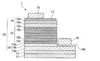
図2及び図3は、本実施形態の発光素子の製造方法の一例を説明するための図であり、基板上にIII族窒化物半導体からなる各層が形成された積層半導体10(図1参照)を用いて発光素子1を構成した例を示す概略図で、図2は平面図、図3は断面図である。
本実施形態の発光素子1は、上記製造方法で製造された積層半導体10のp型半導体層16上に透光性正極17が積層され、その上に正極ボンディングパッド18が形成されるとともに、n型半導体層14のn型コンタクト層14bに形成された露出領域14dに負極19が積層されて概略構成される。
<Laminated structure of light emitting element>
2 and 3 are views for explaining an example of the method for manufacturing the light emitting device of the present embodiment, in which a
In the light emitting device 1 of the present embodiment, a translucent
『透光性正極』
透光性正極17は、上述した積層半導体10のp型半導体層16(p型コンタクト層16b)上に形成される透光性の電極である。
透光性正極17の材質としては、特に限定されず、ITO(In2O3−SnO2)、AZO(ZnO−Al2O3)、IZO(In2O3−ZnO)、GZO(ZnO−Ga2O3)等の材料を、この技術分野でよく知られた慣用の手段で設けることができる。また、その構造も、従来公知の構造を含めて如何なる構造のものも何ら制限なく用いることができる。
また、透光性正極17は、Mgがドープされたp型半導体層16上のほぼ全面を覆うように形成しても構わないし、隙間を開けて格子状や樹形状に形成しても良い。
"Translucent positive electrode"
The translucent
The material of the translucent
The translucent
『正極ボンディングパッド及び負極』
正極ボンディングパッド18は、上述の透光性正極17上に形成される電極である。
正極ボンディングパッド18の材料としては、Au、Al、Ni及びCu等を用いた各種構造が周知であり、これら周知の材料、構造のものを何ら制限無く用いることができる。
正極ボンディングパッド18の厚さは、100〜1000nmの範囲内であることが好ましい。また、ボンディングパッドの特性上、厚さが大きい方が、ボンダビリティーが高くなるため、正極ボンディングパッド18の厚さは300nm以上とすることがより好ましい。さらに、製造コストの観点から500nm以下とすることが好ましい。
“Positive electrode bonding pad and negative electrode”
The positive
As the material of the positive
The thickness of the positive
負極19は、基板11上に、n型半導体層14、発光層15及びp型半導体層16が順次積層された半導体層において、n型半導体層14のn型コンタクト層14bに接するように形成される。このため、負極19を設ける際は、p型半導体層16、発光層15及びn型半導体層14の一部を除去することにより、n型コンタクト層14bの露出領域14dを形成し、この上に負極19を形成する。
負極19の材料としては、各種組成および構造の負極が周知であり、これら周知の負極を何ら制限無く用いることができ、この技術分野でよく知られた慣用の手段で設けることができる。
The
As the material of the
<発光素子の製造方法>
以下に、図2及び図3に示すような発光素子1の製造方法の一例について説明する。
本実施形態の発光素子1の製造方法は、上記製造方法で得られた積層半導体10を用い、該積層半導体10のp型半導体層16上に透光性正極17を積層し、その上に正極ボンディングパッド18を形成するとともに、n型半導体層14のn型コンタクト層14bに形成された露出領域14dに負極19を積層する方法である。
<Method for manufacturing light-emitting element>
Below, an example of the manufacturing method of the light emitting element 1 as shown in FIG.2 and FIG.3 is demonstrated.
The manufacturing method of the light-emitting element 1 of the present embodiment uses the
『透光性正極の形成』
上述のような方法により、基板11上に、バッファ層12及び半導体層が積層された積層半導体10のp型コンタクト層16b上に、ITOからなる透光性正極17を形成する。透光性正極17の形成方法としては、特に限定されず、この技術分野でよく知られた慣用の手段で設けることができる。また、その構造も、従来公知の構造を含めて如何なる構造のものも何ら制限なく用いることができる。
"Formation of translucent positive electrode"
By the method as described above, the translucent
また、上述したように、透光性正極17の材料は、ITOには限定されず、AZO、IZO、GZO等の材料を用いて形成することが可能である。
また、透光性正極17を形成した後、合金化や透明化を目的とした熱アニールを施す場合もあるが、施さなくても構わない。
Further, as described above, the material of the translucent
Further, after forming the translucent
『正極ボンディングパッド及び負極の形成』
積層半導体10上に形成された透光性正極17上に、さらに、正極ボンディングパッド18を形成する。この正極ボンディングパッド18は、例えば、透光性正極17の表面側から順に、Ti、Al、Auの各材料を、従来公知の方法で積層することによって形成することができる。
"Formation of positive electrode bonding pad and negative electrode"
A positive
また、負極19を形成する際は、まず、基板11上に形成された発光層15、p型半導体層16、及びn型半導体層14の一部をドライエッチング等の方法によって除去することにより、n型コンタクト層14bの露出領域14dを形成する(図2及び図3参照)。そして、この露出領域14d上に、例えば、露出領域14d表面側から順に、Ni、Al、Ti、及びAuの各材料を、従来公知の方法で積層することにより、4層構造の負極19を形成することができる。
Further, when forming the
そして、上述のようにして、積層半導体10上に、透光性正極17、正極ボンディングパッド18及び負極19を設けたウェーハを、基板11の裏面を研削及び研磨してミラー状の面とした後、例えば、350μm角の正方形に切断することにより、発光素子チップ(発光素子1)とすることができる。
Then, as described above, after the wafer provided with the translucent
以上説明したような、本実施形態のIII族窒化物半導体発光素子1の製造方法によれば、発光層20の少なくとも一部、本例では、n型半導体層14を構成する下地層14a及びn型コンタクト層14bと、p型半導体層16を構成するp型クラッド層16a及びp型コンタクト層16bの各層を、上記製造方法によって単結晶のIII族窒化物半導体から形成する方法としているので、結晶性の良好なIII族窒化物半導体からなる半導体層を備え、優れた発光特性を有するIII族窒化物半導体発光素子が得られる。
According to the manufacturing method of the group III nitride semiconductor light emitting device 1 of the present embodiment as described above, at least a part of the
[ランプ]
以上説明したような、本発明に係るIII族窒化物半導体発光素子と蛍光体とを組み合わせることにより、当業者周知の手段によってランプを構成することができる。従来より、発光素子と蛍光体と組み合わせることによって発光色を変える技術が知られており、このような技術を何ら制限されることなく採用することが可能である。
例えば、蛍光体を適正に選定することにより、発光素子より長波長の発光を得ることも可能となり、また、発光素子自体の発光波長と蛍光体によって変換された波長とを混ぜることにより、白色発光を呈するランプとすることもできる。
また、ランプとしては、一般用途の砲弾型、携帯のバックライト用途のサイドビュー型、表示器に用いられるトップビュー型等、何れの用途にも用いることができる。
[lamp]
By combining the group III nitride semiconductor light emitting device according to the present invention and the phosphor as described above, a lamp can be configured by means well known to those skilled in the art. Conventionally, a technique for changing the emission color by combining a light emitting element and a phosphor is known, and such a technique can be adopted without any limitation.
For example, it is possible to obtain light having a longer wavelength than that of the light emitting element by appropriately selecting the phosphor, and white light emission by mixing the light emitting wavelength of the light emitting element itself with the wavelength converted by the phosphor. It can also be set as the lamp which exhibits.
Further, the lamp can be used for any purpose such as a general bullet type, a side view type for a portable backlight, and a top view type used for a display.
例えば、図4に示す例のように、同一面電極型のIII族窒化物半導体発光素子1を砲弾型に実装する場合には、2本のフレームの内の一方(図4ではフレーム31)に発光素子1を接着し、また、発光素子1の負極(図3に示す符号19参照)をワイヤー34でフレーム32に接合し、発光素子1の正極ボンディングパッド(図3に示す符号18参照)をワイヤー33でフレーム31に接合する。そして、透明な樹脂からなるモールド35で発光素子1の周辺を封止することにより、図4に示すような砲弾型のランプ3を作成することができる。
本実施形態のランプ3は、上記本実施形態の製造方法によって得られる発光素子1が用いられてなるので、発光特性に優れたものとなる。
For example, as in the example shown in FIG. 4, when mounting the same-surface electrode type group III nitride semiconductor light emitting device 1 in a shell type, one of the two frames (
The
次に、本発明のIII族窒化物半導体の製造方法、及びIII族窒化物半導体発光素子の製造方法を、実施例によりさらに詳細に説明するが、本発明はこれらの実施例にのみ限定されるものではない。 Next, the method for producing a group III nitride semiconductor and the method for producing a group III nitride semiconductor light-emitting device of the present invention will be described in more detail with reference to examples. However, the present invention is limited only to these examples. It is not a thing.
本実施例では、基板11上に各層を成膜し、最終的に、図1に示す断面模式図のようなIII族窒化物化合物半導体発光素子の積層半導体10を作製した。この際、本例では、サファイアからなる基板11のc面上に、バッファ層12としてRFスパッタ法を用いてAlNからなる単結晶層を形成し、その上に、n型半導体層14として、単結晶のGaNからなる下地層14a、及びドナー不純物がドープされたn型コンタクト層14bを反応性スパッタ法で順次成膜し、このn型コンタクト層14b上に、n型クラッド層14cを従来公知のMOCVD法で成膜した。そして、この上に、同様のMOCVD法によって発光層15を成膜し、該発光層15上に、p型半導体層16として、p型クラッド層16a及びp型コンタクト層16bの各層を、反応性スパッタ法を用いてこの順で積層し、積層半導体10のサンプルを作製した。
In this example, each layer was formed on the
[実施例]
本実施例においては、以下に説明するような手順により、積層半導体10のサンプルを作製した。
[Example]
In this example, a sample of the
『バッファ層の形成』
まず、表面を鏡面研磨した直径2インチの(0001)c面サファイアからなる基板11を、フッ酸及び有機溶媒によって洗浄した後、スパッタ装置のチャンバ中へ導入した。この際、スパッタ装置としては、高周波式の電源部を備え、ターゲット内でマグネットを回転させることにより、磁場の掛かる位置を動かすことができる機構を備えたものを使用した。
"Formation of buffer layer"
First, a
そして、スパッタ装置のチャンバ内で基板11を500℃まで加熱し、窒素ガスを15sccmの流量で導入した後、チャンバ内の圧力を1.0Paに保持し、基板11に50Wの高周波バイアスを印加しながら窒素プラズマに晒すことにより、基板11の表面を洗浄した。
Then, the
次いで、基板11の温度を500℃に保持し、チャンバ内にアルゴン及び窒素ガスを導入した。そして、基板11側にバイアスを印加せず、2000Wの高周波パワーを金属Alターゲット側に印加し、炉内の圧力を0.5Paに保ち、Arガスを5sccm、窒素ガスを15sccmの流量で流通させた条件(ガス全体に対する窒素の比は75%)で、サファイアからなる基板11上にAlNからなるバッファ層12を成膜した。この際の成長速度は0.12nm/sであった。
Next, the temperature of the
なお、ターゲット内のマグネットは、基板11の洗浄時、及びバッファ層12の成膜時の何れの際も回転させた。そして、50nmのAlNからなるバッファ層を成膜した後、プラズマを立てるのを停止した。以上の手順により、基板11上に、50nmの厚さの単結晶のAlNからなるバッファ層12を形成した。
The magnet in the target was rotated both when the
『下地層の形成』
次に、バッファ層12が形成された基板11を、反応性スパッタ法によってGaNからなる下地層を成長させるため、図5に示すようなスパッタ装置40のチャンバ41内へ搬送した。ここで、GaNの成膜に使用するスパッタ装置40としては、高周波式の電源部を有し、四角形のGaターゲット内をマグネットがスイープすることで磁場の掛かる位置を動かすことができる機構を備えたものを使用した。また、このスパッタ装置40は、図5に示すように、チャンバ41内の圧力を検知可能な圧力モニタ51からなる窒素量検出手段を備え、また、圧力モニタ51からの検知信号に基づき、反応ガス供給手段50からチャンバ41内に供給される窒素原子含有ガスの流通量を制御する流量制御手段52が備えられている。そして、上記方法で基板11上に成膜されたバッファ層12上に、反応性スパッタ法によってGaN層を成膜した。この際、ターゲット47下方のマグネット42を回転させながら成膜処理を行なうとともに、チャンバ41内の圧力を圧力モニタ51で検知し、この検知信号を流量制御手段52に入力することで、図示略の電磁バルブの開閉動作を行なうことにより、チャンバ41内の窒素量を一定範囲に保持しながら成膜処理を行なった。
"Formation of underlayer"
Next, the
まず、ヒータ44の昇温によって基板11の温度を950℃まで加熱した後、基板11をこの温度に保持しながら、チャンバ41内にアルゴン(Ar)ガス及び窒素(N2)ガスを導入し、1kWの高周波パワーを金属Gaからなるターゲット47側に印加するとともに、100Wのバイアスを基板11側に印加した。次いで、炉内の圧力を0.5〜1Paの範囲に保ちながら、基板41とターゲット47間の距離TSを110mm、Arガスを15sccm、窒素ガスを5sccmの流量で流通させた条件(ガス全体に対する窒素の比は25%)で成膜処理を開始した。そして、チャンバ41内の圧力を圧力モニタで検出し、この検出信号を流量制御手段52に入力することによってチャンバ41内の窒素量が一定範囲となるように制御しながら成膜処理を行なった。
First, after heating the temperature of the
このようにして約60分間の成膜処理を行い、バッファ12層上に、約6μmの膜厚のGaNからなる下地層14aを成膜した後、プラズマを立てるのを停止した。
成膜後にチャンバ41内から取り出した基板は無色透明であり、GaN層(下地層14a)の表面は鏡面であった。また、成膜された下地層14aは、(0002)面のX線ロッキングカーブ半値幅が34秒、(10−10)面のX線ロッキングカーブ半値幅が190秒であり、結晶性に優れた層であることが確認できた。
In this way, the film forming process was performed for about 60 minutes, and after the
The substrate taken out from the
また、さらに、同じスパッタ装置40を用いて、表面にバッファ層12が形成された基板11をチャンバ41内に搬入し、上記同様の下地層14aの成膜処理を、その都度、基板11を入れ替えながら計10回(基板計10枚)行った。この際、チャンバ41の洗浄作業等は行わず、10回の成膜処理を連続して行った。この際、2ラン目以降は、圧力検知の機能により、N2の流量は1ラン目と同じにはならず、少なめとなった。
そして、最後に下地層14aの成膜処理を行なった後にチャンバ41内から取り出した基板は、初回成膜処理の際と同様に無色透明であり、GaN層(下地層14a)の表面は鏡面であった。また、成膜された下地層14aは、(0002)面のX線ロッキングカーブ半値幅が37秒、(10−10)面のX線ロッキングカーブ半値幅が203秒であり、初回成膜処理の際と同様に、結晶性に優れた層が形成されていることが確認できた。
Further, using the
The substrate taken out from the
『n型コンタクト層の形成』
次いで、下地層14aの上に、GaNからなるn型コンタクト層14bを、反応性スパッタ法を用いて形成した。この際、スパッタ装置としては、下地層14aの成膜に用いたスパッタ装置40を同じものを使用し、チャンバ41内の窒素量について同様に制御しながら成膜処理した。
“Formation of n-type contact layer”
Next, an n-
まず、チャンバ41内にアルゴン及び窒素ガスを導入した後、基板11の温度を1000℃まで上昇させた。そして、2kWの高周波パワーを金属Gaからなるターゲット47側に印加し、チャンバ41内の圧力を0.5Paに保ちながら、Arガスを5sccm、窒素ガスを15sccmの流量で流通させた条件(ガス全体に対する窒素の比は75%)で、チャンバ41内の窒素量を上記同様の方法で制御しながら、下地層14a上に、GaNからなるn型コンタクト層14bを成膜した。この際、チャンバ41内にSiからなるドーパント元素を配置することにより、n型コンタクト層14bをなすGaN結晶中にSiをドープした。また、この際の成長速度は、おおよそ2μm/sであった。そして、GaNからなるn型コンタクト層14bを成膜した後、プラズマを立てるのを停止した。
このような手順により、1×1019cm−3の電子濃度を有し、2μmの膜厚のSiドープGaNからなるn型コンタクト層14bを成膜した。
First, after introducing argon and nitrogen gas into the
By such a procedure, an n-
『n型クラッド層の形成』
次いで、n型コンタクト層14bを形成した基板11をMOCVD装置の炉内に搬送し、上記手順で作製したサンプルのn型コンタクト層14b上に、従来公知のMOCVD法を用いて、1×1018cm−3の電子濃度を有する20nmのIn0.1Ga0.9Nからなるn型クラッド層14cを成膜した。
“Formation of n-type cladding layer”
Next, the
『発光層の形成』
次いで、上記手順で作製したサンプルのn型クラッド層14c上に、従来公知のMOCVD法を用いて、GaNからなる障壁層15aと、In0.2Ga0.8Nからなる井戸層15bとから構成され、多重量子井戸構造を有する発光層15を形成した。この、発光層15の形成にあたっては、SiドープGaNからなるn型クラッド層14c上に、まず、障壁層15aを形成し、この障壁層15a上に、In0.2Ga0.8Nからなる井戸層15bを形成した。このような積層手順を5回繰り返した後、5番目に積層した井戸層15b上に、6番目の障壁層15aを形成し、多重量子井戸構造を有する発光層15の両側に障壁層15aを配した構造とした。
"Formation of light emitting layer"
Next, a
すなわち、基板温度を750℃とし、窒素ガスキャリアを流通させながら、アンモニア、TEG及びモノシランを炉内へ供給することにより、16nmの膜厚を有するGaNからなる障壁層15aを形成した。
That is, the
次いで、障壁層15aの成長を終了させた後、基板11の温度や炉内の圧力、キャリアガスの流量や種類はそのままとして、TEG及びTMIのバルブを切り替えてTEG及びTMIを炉内へ供給し、In0.2Ga0.8Nからなる井戸層15bを成長させた。これにより、3nmの膜厚を有する井戸層15bを形成した。
Next, after the growth of the
井戸層15bの成長を終了させた後、再び障壁層15aを成長させた。そして、このような手順を5回繰り返すことにより、5層の障壁層15aと5層の井戸層15bを形成した。さらに、最後に積層した井戸層15b上に、障壁層15aを形成し、発光層15とした。
After the growth of the
『p型クラッド層及びp型コンタクト層の形成』
上述の各工程処理によって得られたウェーハ上に、下地層14a及びn型コンタクト層14bの成膜に用いた装置と同じスパッタ装置40を用いて、p型クラッド層16a及びp型コンタクト層16bからなるp型半導体層16を成膜した。また、この際、p型半導体層16にはMgをドープした。
“Formation of p-type cladding layer and p-type contact layer”
From the p-
そして、最終的に、膜厚が10nmのMgドープAl0.1Ga0.9Nからなるp型クラッド層16aと、膜厚が200nmのMgドープAl0.02Ga0.98Nからなるp型コンタクト層16bとから構成されるp型半導体層16を成膜した。
Finally, a p-
上記工程で得られたMgドープAlGaNからなるp型コンタクト層16bは、p型キャリアを活性化するためのアニール処理を行わなくてもp型を示し、キャリア濃度は3×10¹⁶個/cm3であった。
The p-
上述のようにして作製したLED用のエピタキシャルウェーハは、図1に示す積層半導体10のように、c面を有するサファイアからなる基板11上に、単結晶構造を持つAlN層(中間層12)を形成した後、基板11側から順に、1μmのアンドープGaN層(下地層14a)、5×1018cm−3の電子濃度を持つ2μmのSiドープGaN層(n型コンタクト層14b)、1×1018cm−3の電子濃度を持つ20nmのIn0.01Ga0.99Nクラッド層(n型クラッド層14c)、GaN障壁層に始まってGaN障壁層に終わり、層厚が16nmとされた6層のGaN障壁層(障壁層15a)と、層厚が3nmとされた5層のノンドープのIn0.2Ga0.8N井戸層(井戸層15b)とからなる多重量子井戸構造(発光層15)、膜厚が10nmのMgドープAl0.1Ga0.9Nからなるp型クラッド層16aと、膜厚が200nmのMgドープAl0.02Ga0.98Nからなるp型コンタクト層16bとから構成されるMgドープAlGaN層(p型半導体層16)を積層した構造を有する。
The epitaxial wafer for LED produced as described above has an AlN layer (intermediate layer 12) having a single crystal structure on a
[比較例]
本比較例では、GaNからなる下地層の成膜処理において、図5に示すスパッタ装置40のような圧力モニタ51からなる窒素量検出手段や流量制御手段52が備えられていない従来のスパッタ装置を用い、チャンバ内の窒素量の検出並びに制御を行なわなかった点を除き、上記実施例と同様の手順で基板上にバッファ層を成膜し、その上にGaNからなる下地層及びn型コンタクト層を形成した。
[Comparative example]
In this comparative example, in the film forming process of the underlayer made of GaN, a conventional sputtering apparatus that does not include the nitrogen amount detection means and the flow rate control means 52 including the pressure monitor 51 such as the
成膜後にチャンバ内から取り出した基板は無色透明であり、GaN層(下地層)の表面は鏡面であった。また、成膜された下地層は、(0002)面のX線ロッキングカーブ半値幅が36秒、(10−10)面のX線ロッキングカーブ半値幅が195秒であり、結晶性に優れた層であることが確認できた。 The substrate taken out from the chamber after film formation was colorless and transparent, and the surface of the GaN layer (underlayer) was a mirror surface. In addition, the deposited underlayer has a (0002) plane X-ray rocking curve half width of 36 seconds and a (10-10) plane X-ray rocking curve half width of 195 seconds. It was confirmed that.
さらに、上記実施例と同様、従来のスパッタ装置を用いて、表面にバッファ層が形成された基板をチャンバ内に搬入し、上記同様の下地層の成膜処理を、その都度、基板を入れ替えながら計10回(基板計10枚)行った。この際、チャンバの洗浄作業等は行わず、10回の成膜処理を連続して行った。この際、本比較例では圧力検知の機能がないため、2ラン目以降も、N2の供給量は常に1ラン目と同じであった。
そして、最後に下地層の成膜処理を行なった基板をチャンバ内から取り出した基板の状態を目視確認したところ、基板表面(下地層)が黄色みを帯びた状態であった。また、成膜された下地層は、(0002)面のX線ロッキングカーブ半値幅が150秒、(10−10)面のX線ロッキングカーブ半値幅が340秒であり、初回成膜処理の際に比べ、結晶性の低い層となっていることが明らかとなった。
これは、従来のスパッタ装置のチャンバ内でGaNの成膜処理を繰り返すことにより、チャンバの内壁やシールド部材等にデポジションが付着し、このデポジションが成膜処理の際に分解されることでチャンバ内に窒素が放出され、チャンバ内の雰囲気ガス中における窒素量が過剰な状態となり、GaN結晶(下地層)内に多くのGaの欠損が生じたためと考えられる。
Further, as in the above embodiment, using a conventional sputtering apparatus, a substrate having a buffer layer formed on the surface is carried into the chamber, and the same underlayer film forming process is performed while replacing the substrate each time. A total of 10 times (10 substrates in total) was performed. At this time, the chamber was not cleaned, and 10 film formation processes were continuously performed. At this time, since the pressure detection function is not provided in this comparative example, the supply amount of N 2 was always the same as that in the first run after the second run.
When the substrate on which the substrate layer was finally formed was taken out of the chamber, the state of the substrate was visually confirmed, and the substrate surface (underlayer) was yellowish. In addition, the deposited underlayer has a (0002) plane X-ray rocking curve half-width of 150 seconds and a (10-10) plane X-ray rocking curve half-width of 340 seconds. It became clear that it was a layer with low crystallinity compared with.
This is because the deposition of GaN is repeated in the chamber of a conventional sputtering apparatus, so that the deposition adheres to the inner wall of the chamber, the shield member, etc., and this deposition is decomposed during the deposition process. This is probably because nitrogen was released into the chamber, the amount of nitrogen in the atmospheric gas in the chamber was excessive, and many Ga defects were generated in the GaN crystal (underlayer).
以上の結果により、本発明に係るIII族窒化物半導体の製造方法によって得られるIII族窒化物半導体が、素子特性に優れていることが明らかである。 From the above results, it is clear that the group III nitride semiconductor obtained by the method for producing a group III nitride semiconductor according to the present invention is excellent in device characteristics.
1…III族窒化物半導体発光素子(発光素子)、10…積層半導体(III族窒化物半導体)、11…基板、11a…表面、12…バッファ層、14…n型半導体層、14a…下地層(III族窒化物半導体)、14b…n型コンタクト層(III族窒化物半導体)、15…発光層、16…p型半導体層(III族窒化物半導体)、16a…p型クラッド層(III族窒化物半導体)、16b…p型コンタクト層(III族窒化物半導体)、3…ランプ、40…スパッタ装置、41…チャンバ、47…ターゲット、50…反応ガス供給手段、51…圧力モニタ、52…流量制御手段、60…プラズマ、A…検知信号 DESCRIPTION OF SYMBOLS 1 ... Group III nitride semiconductor light emitting element (light emitting element), 10 ... Laminated semiconductor (Group III nitride semiconductor), 11 ... Substrate, 11a ... Surface, 12 ... Buffer layer, 14 ... N-type semiconductor layer, 14a ... Underlayer (Group III nitride semiconductor), 14b ... n-type contact layer (Group III nitride semiconductor), 15 ... Light emitting layer, 16 ... p-type semiconductor layer (Group III nitride semiconductor), 16a ... p-type cladding layer (Group III) Nitride semiconductor), 16b ... p-type contact layer (group III nitride semiconductor), 3 ... lamp, 40 ... sputtering device, 41 ... chamber, 47 ... target, 50 ... reactive gas supply means, 51 ... pressure monitor, 52 ... Flow rate control means, 60 ... plasma, A ... detection signal
Claims (10)
前記チャンバ内の圧力を圧力モニタで検知し、該圧力モニタの検知信号に基づき、前記反応ガス供給手段から前記チャンバ内に供給する窒素原子含有ガスの流通量を流量制御手段によって制御することを特徴とするIII族窒化物半導体の製造方法。 A substrate and a target containing Ga element are arranged in the chamber, and a nitrogen atom-containing gas and an inert gas are supplied into the chamber by a reaction gas supply means, and a single crystal group III nitride semiconductor is formed on the substrate. A method for producing a group III nitride semiconductor formed by reactive sputtering using plasma,
The pressure in the chamber is detected by a pressure monitor, and the flow rate of the nitrogen atom-containing gas supplied from the reaction gas supply means into the chamber is controlled by the flow rate control means based on the detection signal of the pressure monitor. A method for producing a group III nitride semiconductor.
前記半導体層の少なくとも一部を、請求項1〜5の何れか1項に記載のIII族窒化物半導体の製造方法によって形成することを特徴とするIII族窒化物半導体発光素子の製造方法。 A method of manufacturing a group III nitride semiconductor light-emitting device, wherein a semiconductor layer is formed by sequentially laminating an n-type semiconductor layer, a light-emitting layer, and a p-type semiconductor layer each comprising at least a group III nitride semiconductor on a substrate,
A method for producing a group III nitride semiconductor light-emitting device, wherein at least a part of the semiconductor layer is formed by the method for producing a group III nitride semiconductor according to any one of claims 1 to 5.
前記チャンバ内の圧力を検知する圧力モニタが備えられているとともに、該圧力モニタの検知信号に基づき、前記反応ガス供給手段から前記チャンバ内に供給される窒素原子含有ガスの流通量を制御する流量制御手段が備えられていることを特徴とするIII族窒化物半導体製造装置。 A substrate and a target containing Ga element are disposed in the chamber, and a reactive gas supply means for supplying a nitrogen atom-containing gas and an inert gas is provided in the chamber, and a single crystal group III nitride semiconductor is provided on the substrate. Is a group III nitride semiconductor manufacturing apparatus that is formed by a reactive sputtering method using plasma,
A flow rate monitor that detects a pressure in the chamber and controls a flow rate of a nitrogen atom-containing gas supplied from the reaction gas supply means into the chamber based on a detection signal of the pressure monitor. A group III nitride semiconductor manufacturing apparatus comprising a control means.
Priority Applications (1)
| Application Number | Priority Date | Filing Date | Title |
|---|---|---|---|
| JP2007332678A JP2009155672A (en) | 2007-12-25 | 2007-12-25 | Method for manufacturing group-iii nitride semiconductor, method for manufacturing light-emitting device of group-iii nitride semiconductor, apparatus for manufacturing group-iii nitride semiconductor, group-iii nitride semiconductor and light-emitting device of group-iii nitride semiconductor, and lamp |
Applications Claiming Priority (1)
| Application Number | Priority Date | Filing Date | Title |
|---|---|---|---|
| JP2007332678A JP2009155672A (en) | 2007-12-25 | 2007-12-25 | Method for manufacturing group-iii nitride semiconductor, method for manufacturing light-emitting device of group-iii nitride semiconductor, apparatus for manufacturing group-iii nitride semiconductor, group-iii nitride semiconductor and light-emitting device of group-iii nitride semiconductor, and lamp |
Publications (1)
| Publication Number | Publication Date |
|---|---|
| JP2009155672A true JP2009155672A (en) | 2009-07-16 |
Family
ID=40959991
Family Applications (1)
| Application Number | Title | Priority Date | Filing Date |
|---|---|---|---|
| JP2007332678A Pending JP2009155672A (en) | 2007-12-25 | 2007-12-25 | Method for manufacturing group-iii nitride semiconductor, method for manufacturing light-emitting device of group-iii nitride semiconductor, apparatus for manufacturing group-iii nitride semiconductor, group-iii nitride semiconductor and light-emitting device of group-iii nitride semiconductor, and lamp |
Country Status (1)
| Country | Link |
|---|---|
| JP (1) | JP2009155672A (en) |
Cited By (3)
| Publication number | Priority date | Publication date | Assignee | Title |
|---|---|---|---|---|
| JP2012174796A (en) * | 2011-02-18 | 2012-09-10 | Ulvac Japan Ltd | Method of forming gallium nitride film, and device of forming gallium nitride film |
| JP2012246204A (en) * | 2011-05-31 | 2012-12-13 | Ulvac Japan Ltd | Method for forming gallium nitride columnar structure and apparatus for forming gallium nitride columnar structure |
| JP7173621B2 (en) | 2018-05-18 | 2022-11-16 | 中国科学院蘇州納米技術与納米▲ファン▼生研究所 | Method for manufacturing gallium oxide thin film containing sapphire substrate |
Citations (5)
| Publication number | Priority date | Publication date | Assignee | Title |
|---|---|---|---|---|
| JPS6334931A (en) * | 1986-07-29 | 1988-02-15 | Nec Corp | Apparatus for manufacturing semiconductor |
| JPH08120446A (en) * | 1994-10-21 | 1996-05-14 | Ube Ind Ltd | Formation of titanium nitride-aluminum film |
| JPH08181073A (en) * | 1994-12-21 | 1996-07-12 | Canon Inc | Semiconductor wafer and crystal growth method |
| JP2001035805A (en) * | 1999-07-19 | 2001-02-09 | Sony Corp | Iii group nitride compound semiconductor thin film, method of forming same, semiconductor device and manufacture thereof |
| WO2007129773A1 (en) * | 2006-05-10 | 2007-11-15 | Showa Denko K.K. | Iii nitride compound semiconductor laminated structure |
-
2007
- 2007-12-25 JP JP2007332678A patent/JP2009155672A/en active Pending
Patent Citations (5)
| Publication number | Priority date | Publication date | Assignee | Title |
|---|---|---|---|---|
| JPS6334931A (en) * | 1986-07-29 | 1988-02-15 | Nec Corp | Apparatus for manufacturing semiconductor |
| JPH08120446A (en) * | 1994-10-21 | 1996-05-14 | Ube Ind Ltd | Formation of titanium nitride-aluminum film |
| JPH08181073A (en) * | 1994-12-21 | 1996-07-12 | Canon Inc | Semiconductor wafer and crystal growth method |
| JP2001035805A (en) * | 1999-07-19 | 2001-02-09 | Sony Corp | Iii group nitride compound semiconductor thin film, method of forming same, semiconductor device and manufacture thereof |
| WO2007129773A1 (en) * | 2006-05-10 | 2007-11-15 | Showa Denko K.K. | Iii nitride compound semiconductor laminated structure |
Cited By (3)
| Publication number | Priority date | Publication date | Assignee | Title |
|---|---|---|---|---|
| JP2012174796A (en) * | 2011-02-18 | 2012-09-10 | Ulvac Japan Ltd | Method of forming gallium nitride film, and device of forming gallium nitride film |
| JP2012246204A (en) * | 2011-05-31 | 2012-12-13 | Ulvac Japan Ltd | Method for forming gallium nitride columnar structure and apparatus for forming gallium nitride columnar structure |
| JP7173621B2 (en) | 2018-05-18 | 2022-11-16 | 中国科学院蘇州納米技術与納米▲ファン▼生研究所 | Method for manufacturing gallium oxide thin film containing sapphire substrate |
Similar Documents
| Publication | Publication Date | Title |
|---|---|---|
| JP5272390B2 (en) | Group III nitride semiconductor manufacturing method, group III nitride semiconductor light emitting device manufacturing method, group III nitride semiconductor light emitting device, and lamp | |
| JP5246219B2 (en) | Group III nitride semiconductor device manufacturing method and group III nitride semiconductor light emitting device manufacturing method | |
| JP4191227B2 (en) | Group III nitride semiconductor light emitting device manufacturing method, group III nitride semiconductor light emitting device, and lamp | |
| JP5049659B2 (en) | Group III nitride semiconductor manufacturing method, group III nitride semiconductor light emitting device manufacturing method, group III nitride semiconductor light emitting device, and lamp | |
| TWI491064B (en) | Group iii nitride semiconductor light emitting device, process for producing the same, and lamp | |
| KR101074178B1 (en) | Method for manufacturing group ⅲ nitride compound semiconductor light-emitting device, group ⅲ nitride compound semiconductor light-emitting device, and lamp | |
| WO2010032423A1 (en) | Method for manufacturing iii nitride semiconductor light emitting element, iii nitride semiconductor light emitting element and lamp | |
| WO2009154129A1 (en) | Iii-group nitride semiconductor light emitting element, method for manufacturing the element, and lamp | |
| US8227359B2 (en) | Method for manufacturing group III nitride semiconductor layer, method for manufacturing group III nitride semiconductor light-emitting device, and group III nitride semiconductor light-emitting device, and lamp | |
| JP2009081406A (en) | Group iii nitride semiconductor light-emitting device, method for manufacturing thereof, and lamp | |
| JP2009277882A (en) | Method of manufacturing group iii nitride semiconductor light emitting element, group iii nitride semiconductor light emitting element, and lamp | |
| JP2009295753A (en) | Method of manufacturing group iii nitride semiconductor light-emitting device and group iii nitride semiconductor light-emitting device, and lamp | |
| JP2008177525A (en) | Method for manufacturing group iii nitride compound semiconductor light-emitting element, the group iii nitride compound semiconductor light-emitting element and lamp | |
| JP2011082570A (en) | Method of manufacturing group iii nitride semiconductor light emitting device | |
| JP2008305967A (en) | Device and method for manufacturing group iii nitride semiconductor layer, manufacturing method for group iii nitride semiconductor light-emitting element and group iii nitride semiconductor light-emitting element and lamp | |
| JP2009155672A (en) | Method for manufacturing group-iii nitride semiconductor, method for manufacturing light-emitting device of group-iii nitride semiconductor, apparatus for manufacturing group-iii nitride semiconductor, group-iii nitride semiconductor and light-emitting device of group-iii nitride semiconductor, and lamp | |
| JP2008135463A (en) | Manufacturing method of group iii nitride semiconductor, manufacturing method of group iii nitride semiconductor light-emitting element, group iii nitride semiconductor light-emitting element and lamp | |
| JP2008106316A (en) | Method for manufacturing group iii nitride compound semiconductor light-emitting device, group iii nitride compound semiconductor light-emitting device, and lamp | |
| JP2009161434A (en) | Method for manufacturing group iii nitride semiconductor crystal and group iii nitride semiconductor crystal | |
| JP2008294449A (en) | Method for manufacturing group iii nitride semiconductor light emitting element, group iii nitride semiconductor light emitting element and lamp | |
| JP5179055B2 (en) | Group III nitride semiconductor manufacturing method, group III nitride semiconductor light emitting device manufacturing method, group III nitride semiconductor light emitting device, and lamp | |
| JP2008159954A (en) | Manufacturing method of group iii nitride semiconductor, manufacturing method of group iii nitride semiconductor light-emitting element, group iii nitride semiconductor light-emitting element and lamp | |
| JP2008198705A (en) | Method for manufacturing group iii nitride semiconductor light-emitting device, group iii nitride semiconductor light-emitting device, and lamp | |
| JP2008306113A (en) | Manufacturing method of group iii nitride semiconductor, manufacturing method of group iii nitride semiconductor light emitting element, group iii nitride semiconductor light emitting element and lamp | |
| JP2009049234A (en) | Method and device for manufacturing group iii nitride semiconductor, method of manufacturing group iii nitride semiconductor element and group iii nitride semiconductor element and lamp |
Legal Events
| Date | Code | Title | Description |
|---|---|---|---|
| A621 | Written request for application examination |
Free format text: JAPANESE INTERMEDIATE CODE: A621 Effective date: 20100909 |
|
| A977 | Report on retrieval |
Free format text: JAPANESE INTERMEDIATE CODE: A971007 Effective date: 20120113 |
|
| A131 | Notification of reasons for refusal |
Free format text: JAPANESE INTERMEDIATE CODE: A131 Effective date: 20120124 |
|
| A02 | Decision of refusal |
Free format text: JAPANESE INTERMEDIATE CODE: A02 Effective date: 20120724 |