JP2009130084A - Semiconductor device - Google Patents
Semiconductor device Download PDFInfo
- Publication number
- JP2009130084A JP2009130084A JP2007302685A JP2007302685A JP2009130084A JP 2009130084 A JP2009130084 A JP 2009130084A JP 2007302685 A JP2007302685 A JP 2007302685A JP 2007302685 A JP2007302685 A JP 2007302685A JP 2009130084 A JP2009130084 A JP 2009130084A
- Authority
- JP
- Japan
- Prior art keywords
- type
- semiconductor layer
- pin diode
- layer
- intrinsic semiconductor
- Prior art date
- Legal status (The legal status is an assumption and is not a legal conclusion. Google has not performed a legal analysis and makes no representation as to the accuracy of the status listed.)
- Pending
Links
Images


Abstract
Description
本発明は、半導体装置技術に関し、特に、PIN接合を有する半導体装置に適用して有効な技術に関するものである。 The present invention relates to a semiconductor device technology, and more particularly to a technology effective when applied to a semiconductor device having a PIN junction.
近年の高度な情報化社会の発展に伴い、移動通信機器端末などの性能の向上が要求されている。例えば、デジタル携帯電話などでは、小型化、低消費電力化およびマルチバンド化が急速に進んでいる。 With the development of an advanced information society in recent years, it is required to improve the performance of mobile communication device terminals. For example, in digital cellular phones and the like, miniaturization, low power consumption, and multibanding are rapidly progressing.
ここで、一般的なデジタル携帯電話においては、信号を送信するための送信用回路と、受信した信号を処理する受信用回路と、外部からこれらの回路に信号を受発信するためのアンテナとを有している。そして、送信時には送信用回路からアンテナへと信号を伝達し、受信用回路には伝達されないようにする必要がある一方で、受信時にはアンテナから受信用回路へと信号を伝達し、送信用回路には伝達されないようにする必要がある。即ち、信号処理回路内では高周波信号の伝達経路を切り替える必要がある。この目的を満たす素子として、PN接合ダイオード(以下、PNダイオード)が用いられている。 Here, in a general digital mobile phone, a transmission circuit for transmitting signals, a reception circuit for processing received signals, and an antenna for receiving and transmitting signals to these circuits from the outside are provided. Have. When transmitting, it is necessary to transmit a signal from the transmitting circuit to the antenna and not to the receiving circuit. On receiving, it transmits a signal from the antenna to the receiving circuit and to the transmitting circuit. Must not be communicated. That is, it is necessary to switch the transmission path of the high frequency signal in the signal processing circuit. A PN junction diode (hereinafter referred to as PN diode) is used as an element that satisfies this purpose.
2端子からなるPNダイオードは、その2端子への印加電圧のバイアスに対し、正負いずれかの極性に対して電流を通過させ(順方向、オン状態)、他方の極性に対して電流を遮断する(逆方向、オフ状態)といった、所謂整流特性を有する。この整流特性を利用して、送信時、アンテナと送信用回路とを導通させるときは、アンテナと受信用回路とを遮断し、受信時、アンテナと受信用回路とを導通させるときは、アンテナと送信用回路とを遮断するようにする。 A two-terminal PN diode allows current to pass in either positive or negative polarity with respect to the bias of the voltage applied to the two terminals (forward direction, on state), and interrupts current for the other polarity. It has so-called rectification characteristics such as (reverse direction, off state). Using this rectification characteristic, when the antenna and the transmission circuit are made conductive at the time of transmission, the antenna and the reception circuit are shut off, and at the time of reception, the antenna and the reception circuit are made conductive. Shut off the transmission circuit.
上記のようにアンテナ切り換え用途のPNダイオードの特性としては、順方向特性(オン時)は低抵抗であることが望ましい。なぜなら、順方向としてPNダイオードに信号を通過させるときは、信号の損失(ロス)をできるだけ少なくすることが望ましく、順方向抵抗は低い方が良いからである。更に、逆方向特性(オフ時)は低容量であることが望ましい。なぜなら、逆方向としてPNダイオードに信号を遮断さるときは、容量としてのPNダイオードを充放電する時間をできるだけ短くすることが望ましく、逆方向容量は低い方が良いからである。 As described above, as a characteristic of the PN diode for antenna switching, it is desirable that the forward characteristic (when turned on) has a low resistance. This is because when a signal is passed through the PN diode in the forward direction, it is desirable to reduce the loss of the signal as much as possible, and a lower forward resistance is better. Furthermore, it is desirable that the reverse characteristic (when off) is a low capacity. This is because when the signal is cut off from the PN diode in the reverse direction, it is desirable to shorten the charge / discharge time of the PN diode as a capacitor as much as possible, and a lower reverse capacitance is better.
上記の特性が要求されるPNダイオードとして、PN接合を形成するP領域とN領域との間に、真性(Intrinsic)半導体領域(以下、真性領域)を挟んだ、PIN接合ダイオード(以下、PINダイオード)の適用が実用化されている。真性領域は、外因性の不純物濃度が低く、逆方向電圧印加時に空乏層が広がり易い。従って、電気容量は低下するからである。 As a PN diode that requires the above characteristics, a PIN junction diode (hereinafter referred to as a PIN diode) in which an intrinsic semiconductor region (hereinafter referred to as an intrinsic region) is sandwiched between a P region and an N region that form a PN junction. ) Has been put to practical use. In the intrinsic region, the concentration of exogenous impurities is low, and the depletion layer tends to spread when a reverse voltage is applied. Therefore, the electric capacity is reduced.
高不純物濃度の半導体基板上に形成した、真性領域、および、基板と逆導電型の高不純物濃度の半導体領域の積層構造を有するPINダイオードなどが、例えば、特開2002−124686号公報(特許文献1)、または、特開2005−340484号公報(特許文献2)などに開示されている。
本発明者らが、例えば携帯電話機器などへの導入を検討したPINダイオードの構造を、図12に示す。基板でありN型の半導体領域であるN型カソード基板NCx、真性半導体である真性半導体層ILx、および、P型の半導体領域であるP型アノード層PAxの三層構造により、PINダイオード1xの主要な部分が構成されている。
FIG. 12 shows the structure of a PIN diode that the present inventors have studied for introduction into, for example, a mobile phone device. The three-layer structure of the N-type cathode substrate NCx, which is a substrate and an N-type semiconductor region, the intrinsic semiconductor layer ILx, which is an intrinsic semiconductor, and the P-type anode layer PAx, which is a P-type semiconductor region, makes the main of the
また、N型カソード基板NCxおよびP型アノード層PAxには、電極として、それぞれカソード電極ECxおよびアノード電極EAxが形成されている。また、真性半導体層ILxおよびP型アノード層PAxには、表面からN型カソード基板NCxに達するトレンチTxが形成されている。トレンチTxおよびその周辺は、保護膜PVxが形成されている。 In addition, a cathode electrode ECx and an anode electrode EAx are formed as electrodes on the N-type cathode substrate NCx and the P-type anode layer PAx, respectively. In addition, trenches Tx reaching from the surface to the N-type cathode substrate NCx are formed in the intrinsic semiconductor layer ILx and the P-type anode layer PAx. A protective film PVx is formed around the trench Tx and its periphery.
ここで、上記のように、PINダイオード1xはPN接合の間に真性領域を有している。このようなPINダイオード1xに逆方向バイアスを印加すると、真性領域に広がる空乏層が広く、電気容量は通常のPNダイオードに比べて低くなることは上記で説明した通りである。一方、不純物濃度が極端に低い真性領域を有するPINダイオード1xは、順方向バイアス時の抵抗値が高くなってしまうことが懸念される。そこで、逆方向低容量特性を有するPINダイオード1xにおいては、順方向特性を低抵抗化するような技術動向となっている。特に、近年の携帯通信機器の多機能化により、低消費電力化が強く望まれており、このような要求からも、低抵抗化の必要性が高くなってきている。
Here, as described above, the
しかし、本発明者らは、上記構造のPINダイオード1xの順方向特性を低抵抗にする技術を検討し、以下のような課題を見出した。即ち、順方向特性の低抵抗化のためには、外因性不純物濃度の低い真性半導体層ILxの中に、N型カソード基板NCxおよびP型アノード層PAxから、より多くのキャリアを注入し得る構造とすることが有効であると、本発明者らは着想した。
However, the present inventors have studied a technique for reducing the forward characteristic of the
本発明者らの検討によれば、P型アノード層PAxと真性半導体層ILxとの接合面積を広げることで、抵抗値が低下し得ることが見出された。しかしながら、P型アノード層PAxと真性半導体層ILxとの接合面積を広げることは、当該PINダイオード1xの逆方向特性において、電荷蓄積部の面積が増加することを意味し、即ち、電気容量の増加を引き起こす。このように、単に接合面積を拡大するという手法では、順方向抵抗値と、逆方向容量値とはトレードオフの関係にあることが、本発明者らの検討により明らかとなった。
According to the study by the present inventors, it has been found that the resistance value can be lowered by increasing the junction area between the P-type anode layer PAx and the intrinsic semiconductor layer ILx. However, increasing the junction area between the P-type anode layer PAx and the intrinsic semiconductor layer ILx means that the area of the charge storage portion is increased in the reverse characteristics of the
そこで、本発明の目的は、PINダイオードを有する半導体装置において、PINダイオードの順方向特性を低抵抗化させる技術を提供することにある。 Accordingly, an object of the present invention is to provide a technique for reducing the forward characteristics of a PIN diode in a semiconductor device having the PIN diode.
本発明の前記ならびにその他の目的と新規な特徴は、本明細書の記述および添付図面から明らかになるであろう。 The above and other objects and novel features of the present invention will be apparent from the description of this specification and the accompanying drawings.
本願においては、複数の発明が開示されるが、そのうちの一実施例の概要を簡単に説明すれば以下の通りである。 In the present application, a plurality of inventions are disclosed. An outline of one embodiment of the inventions will be briefly described as follows.
即ち、第1導電型の第1半導体層と、第2導電型の第2半導体層と、これらの間に各々に接触した状態で設けられ、真性半導体である第1導電型の第3半導体層とを含むダイオードを有し、第2半導体層は、第3半導体層の主面から所望の深さに渡って形成され、第2半導体層の外周は、第3半導体層の主面内において第3半導体層のダイオード形成部の外周から内側に離れた位置で終端している。 That is, a first conductive type first semiconductor layer, a second conductive type second semiconductor layer, and a first conductive type third semiconductor layer that is provided in contact with each other and is an intrinsic semiconductor. The second semiconductor layer is formed to a desired depth from the main surface of the third semiconductor layer, and the outer periphery of the second semiconductor layer is formed in the main surface of the third semiconductor layer. The three semiconductor layers are terminated at positions away from the outer periphery of the diode forming portion.
本願において開示される複数の発明のうち、上記一実施例により得られる効果を代表して簡単に説明すれば以下のとおりである。 Of the plurality of inventions disclosed in the present application, effects obtained by the above-described embodiment will be briefly described as follows.
即ち、PINダイオードを有する半導体装置において、PINダイオードの順方向特性を低抵抗化させることができる。 That is, in a semiconductor device having a PIN diode, the forward characteristic of the PIN diode can be reduced.
以下の実施の形態においては便宜上その必要があるときは、複数のセクションまたは実施の形態に分割して説明するが、特に明示した場合を除き、それらはお互いに無関係なものではなく、一方は他方の一部または全部の変形例、詳細、補足説明等の関係にある。また、以下の実施の形態において、要素の数等(個数、数値、量、範囲等を含む)に言及する場合、特に明示した場合および原理的に明らかに特定の数に限定される場合等を除き、その特定の数に限定されるものではなく、特定の数以上でも以下でも良い。さらに、以下の実施の形態において、その構成要素(要素ステップ等も含む)は、特に明示した場合および原理的に明らかに必須であると考えられる場合等を除き、必ずしも必須のものではないことは言うまでもない。同様に、以下の実施の形態において、構成要素等の形状、位置関係等に言及するときは、特に明示した場合および原理的に明らかにそうでないと考えられる場合等を除き、実質的にその形状等に近似または類似するもの等を含むものとする。このことは、上記数値および範囲についても同様である。また、本実施の形態を説明するための全図において同一機能を有するものは同一の符号を付すようにし、その繰り返しの説明は可能な限り省略するようにしている。以下、本発明の実施の形態を図面に基づいて詳細に説明する。 In the following embodiments, when it is necessary for the sake of convenience, the description will be divided into a plurality of sections or embodiments. However, unless otherwise specified, they are not irrelevant to each other. There are some or all of the modifications, details, supplementary explanations, and the like. Further, in the following embodiments, when referring to the number of elements (including the number, numerical value, quantity, range, etc.), especially when clearly indicated and when clearly limited to a specific number in principle, etc. Except, it is not limited to the specific number, and may be more or less than the specific number. Further, in the following embodiments, the constituent elements (including element steps and the like) are not necessarily indispensable unless otherwise specified and clearly considered essential in principle. Needless to say. Similarly, in the following embodiments, when referring to the shapes, positional relationships, etc. of the components, etc., the shapes are substantially the same unless otherwise specified, or otherwise apparent in principle. And the like are included. The same applies to the above numerical values and ranges. Also, components having the same function are denoted by the same reference symbols throughout the drawings for describing the embodiments, and the repetitive description thereof is omitted as much as possible. Hereinafter, embodiments of the present invention will be described in detail with reference to the drawings.
(実施の形態1)
本実施の形態1のダイオード(半導体装置)は、例えばデジタル携帯電話の高周波スイッチ用のPINダイオードである。このようなPINダイオードにおいて、逆方向特性における電気容量を増加させることなく、順方向特性を低抵抗化する技術を例示する。
(Embodiment 1)
The diode (semiconductor device) of the first embodiment is, for example, a PIN diode for a high frequency switch of a digital mobile phone. In such a PIN diode, a technique for reducing the resistance of the forward characteristics without increasing the capacitance in the reverse characteristics will be exemplified.
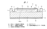
図1には、本実施の形態1のPINダイオード1Aの平面図を示している。ここでは特に、異なる半導体領域の平面的な境界線のみを示し、絶縁膜の領域、導体膜の領域などは省略している。更に、図2には、図1におけるx1−x1線の断面を矢印の方向に見た要部断面図を示している。
FIG. 1 is a plan view of the
本実施の形態1のPINダイオード1Aは、N型(第1導電型)の半導体基板としてのN型カソード基板(第1半導体層)NCと、P型(第2導電型)のP型アノード層(第2半導体層)PAとを有し、これらの間に各々に接触した状態で設けられた、N型の真性半導体層であるN型真性半導体層(第3半導体層)ILを有している。
The
N型とは、例えばIV族の元素からなるシリコンなどにおいて、リン(P)やヒ素(As)などのV族元素を、III族の元素よりも多く含有した状態であり、多数キャリアが電子であるような半導体材料の導電型を表す。また、P型とは、IV族シリコンなどにおいて、ホウ素(B)などのIII族元素を、V族元素よりも多く含有した状態であり、多数キャリアが正孔(ホール)であるような半導体材料の導電型を表す。 The N-type is a state in which, for example, silicon composed of Group IV elements contains more Group V elements such as phosphorus (P) and arsenic (As) than Group III elements, and majority carriers are electrons. It represents the conductivity type of a certain semiconductor material. The P-type is a semiconductor material in which group III elements such as boron (B) are contained more than group V elements in group IV silicon and the like, and the majority carriers are holes. Represents the conductivity type.
N型カソード基板NCは、例えばシリコン(Si)単結晶により形成されており、厚さ方向に沿って互いに反対側に位置する表面S1および裏面S2を有する。このN型カソード基板NCの平面形状は、例えば四角形上に形成されている。 The N-type cathode substrate NC is formed of, for example, silicon (Si) single crystal, and has a front surface S1 and a back surface S2 located on opposite sides along the thickness direction. The planar shape of the N-type cathode substrate NC is formed, for example, on a quadrangle.
N型カソード基板NCの表面S1上には、N型真性半導体層ILが形成されている。N型真性半導体層ILは、上記N型カソード基板NCと同様に、例えばN型のシリコン単結晶により形成されているが、その不純物濃度は、N型カソード基板NCとは異なり、真性半導体となる条件を満たすように設定されている。 On the surface S1 of the N-type cathode substrate NC, an N-type intrinsic semiconductor layer IL is formed. The N-type intrinsic semiconductor layer IL is formed of, for example, an N-type silicon single crystal similarly to the N-type cathode substrate NC, but its impurity concentration is an intrinsic semiconductor unlike the N-type cathode substrate NC. It is set to satisfy the conditions.
ここで、真性半導体とは、以下のように定義される半導体であるとする。単結晶よりなる半導体材料において、結合状態にある安定したエネルギーを持った電子は、有限の温度では熱擾乱によって伝導電子(または自由電子)となるエネルギーに励起される。結合状態にある電子が自由電子となるので、このとき同数の正孔が生成される。そこで、真性半導体とは、注入(またはドーピング)された外因性不純物の濃度(不純物濃度)が、この熱的に発生した電子、正孔濃度に比べて少ない半導体のことを言うこととする。もちろん、不純物を含まない半導体を排除するものではない。 Here, the intrinsic semiconductor is assumed to be a semiconductor defined as follows. In a semiconductor material made of a single crystal, electrons having stable energy in a bonded state are excited to energy that becomes conduction electrons (or free electrons) by thermal disturbance at a finite temperature. Since the electrons in the coupled state become free electrons, the same number of holes are generated at this time. Therefore, an intrinsic semiconductor means a semiconductor in which the concentration (impurity concentration) of implanted (or doped) extrinsic impurities is smaller than the concentration of electrons and holes generated thermally. Of course, this does not exclude semiconductors that do not contain impurities.
このN型真性半導体層ILには、N型真性導通部分(ダイオード形成部)IDの外周に沿って、N型真性半導体層ILの主面SILからN型カソード基板NCの表面S1に達するようなトレンチ(溝)Tを有している。ここで、このN型真性半導体層ILにおいて、トレンチTに囲まれた部分がN型真性導通部分IDである。言い換えれば、N型真性導通部分IDは、平面的に見て、トレンチTによって、N型カソード基板NCの外周から隔離されている。N型真性導通部分IDの主面SILの平面形状は、例えば矩形形状である。 The N-type intrinsic semiconductor layer IL extends from the main surface SIL of the N-type intrinsic semiconductor layer IL to the surface S1 of the N-type cathode substrate NC along the outer periphery of the N-type intrinsic conducting portion (diode forming portion) ID. A trench (groove) T is provided. Here, in the N-type intrinsic semiconductor layer IL, a portion surrounded by the trench T is an N-type intrinsic conduction portion ID. In other words, the N-type intrinsic conductive portion ID is isolated from the outer periphery of the N-type cathode substrate NC by the trench T in a plan view. The planar shape of the main surface SIL of the N-type intrinsic conductive portion ID is, for example, a rectangular shape.
N型真性導通部分IDは、上記トレンチTを隔てて平面枠状のN型真性半導体層ILが残されているが、この部分は素子自体として機能する部分ではない。 In the N-type intrinsic conductive portion ID, the planar frame-shaped N-type intrinsic semiconductor layer IL is left with the trench T interposed therebetween, but this portion does not function as the element itself.
後に詳細を記すように、本実施の形態1のPINダイオード1Aにおいては、上記のN型真性導通部分IDが、ダイオード素子のPIN接合を構成する要素となる。このように、素子の構成要素であるN型真性導通部分IDを、トレンチTによって、N型カソード基板NCの外周から隔離することで、以下のような構造とすることができる。
As will be described in detail later, in the
N型カソード基板NCは、PINダイオード1Aを構成する基板として用いており、製造工程中は、半導体ウェハと称される平面略円形状の薄板上に、同様の構造を一括して形成するようにして扱われる。そして、後に詳細を示すような工程により、所望の構成を形成した後、スクライバと称される裁断機によって、個々に切り分けられる(ダイシング)。このとき、本発明者らの検討によれば、素子の構成要素として用いるN型真性半導体層ILがN型カソード基板NCの外周にまで達していると、ダイシング時の機械的な応力や直接的な汚染により、欠陥が生じるという。このような結晶欠陥は、注入されたキャリアのトラップ準位となって、キャリアの輸送を妨げる。結果として、PINダイオードの順方向特性における抵抗値を上昇させる原因となるという。
The N-type cathode substrate NC is used as a substrate constituting the
そこで、本実施の形態1のPINダイオード1Aでは、N型真性導通部分IDを設け、この領域を、ダイシングの対象となるN型カソード基板NCの外周から、トレンチTによって隔離させている。そして、このN型真性導通部分にダイオード素子のPIN接合を形成することで、特性に影響する真性領域には、ダイシングによる結晶欠陥が生じ難い構造とすることができる。結果として、PINダイオードの順方向特性における抵抗値を低下させることができる。
Therefore, in the
また、上記のように、N型真性導通部分IDをダイシング領域から隔離する目的で形成されるトレンチTは、ウェットエッチング、ドライエッチング、または、これらの組み合わせといった、化学的なエッチングプロセスによって形成しても良い。これにより、N型真性導通部分IDの側壁内に、結晶欠陥を生じ難くなる。結果として、PINダイオードの順方向特性における抵抗値をより低下させることができる。 Further, as described above, the trench T formed for the purpose of isolating the N-type intrinsic conductive portion ID from the dicing region is formed by a chemical etching process such as wet etching, dry etching, or a combination thereof. Also good. Thereby, it becomes difficult to produce a crystal defect in the side wall of the N-type intrinsic conduction portion ID. As a result, the resistance value in the forward characteristic of the PIN diode can be further reduced.
N型真性半導体層ILのN型真性導通部分IDの表面は、保護膜PVで覆われている。ここでは、N型真性導通部分IDが露出しないように、段差部やトレンチTの内壁などを完全に覆うようにして、保護膜PVが形成されている。 The surface of the N-type intrinsic conductive portion ID of the N-type intrinsic semiconductor layer IL is covered with a protective film PV. Here, the protective film PV is formed so as to completely cover the stepped portion and the inner wall of the trench T so that the N-type intrinsic conductive portion ID is not exposed.
本実施の形態1において、保護膜PVとしては、例えば、以下に示す3種の膜の積層構造であるとする。1層目は、N型真性半導体層ILを構成する材料である単結晶シリコン上に安定に形成することができる、酸化シリコン膜を主体とする酸化膜である。2層目は、種々のイオンなど、外部からの外因性電荷を捕獲(ゲッタリング)する機能を有する、PSG(Phospho-Silicate Glass)を主体とするケイ酸塩ガラス膜である。3層目は、水分などの浸入を防ぐ機能を有する、窒化シリコン膜を主体とする窒化膜である。なお、3層目の窒化シリコン膜は、段差部の被覆性(ステップカバレージ)を良くするために、例えば、低圧の化学気相成長(CVD:Chemical Vapor Deposition)法などによって形成したものを適用する。 In the first embodiment, the protective film PV is, for example, a laminated structure of the following three types of films. The first layer is an oxide film mainly composed of a silicon oxide film that can be stably formed on single crystal silicon which is a material constituting the N-type intrinsic semiconductor layer IL. The second layer is a silicate glass film mainly composed of PSG (Phospho-Silicate Glass) having a function of trapping (gettering) external charges such as various ions. The third layer is a nitride film mainly composed of a silicon nitride film having a function of preventing intrusion of moisture and the like. The third silicon nitride film is formed by, for example, a low-pressure chemical vapor deposition (CVD) method in order to improve the coverage (step coverage) of the stepped portion. .
以上のような保護膜PVによって、N型真性半導体層ILの主面SILを覆うことで、PIN接合の構成要素であるN型真性導通部分IDなどを、外部からのイオンの侵入や水分の浸入から防ぐことができる。これにより、PIN接合において真性領域に注入されたキャリアが、外因性の電荷や汚染などにより輸送を妨げられ難くなる。結果として、PINダイオードの順方向特性における抵抗値をさらに低下させることができる。 By covering the main surface SIL of the N-type intrinsic semiconductor layer IL with the protective film PV as described above, the N-type intrinsic conductive portion ID, which is a component of the PIN junction, can enter ions from the outside or moisture can enter. Can prevent from. This makes it difficult for carriers injected into the intrinsic region in the PIN junction to be prevented from being transported by exogenous charges or contamination. As a result, the resistance value in the forward characteristic of the PIN diode can be further reduced.
また、本発明者らが検討した技術によれば、上記と同様の外因性の電荷や汚染の侵入を防止する目的で、真性領域の表面に基板(カソード部)と同じ導電型の拡散層を形成し、真性領域表面の安定化を図る方法がある。ここで、追加した拡散層は、真性半導体状態よりも高い不純物濃度を有する半導体領域であるという。しかし、この技術を適用したPINダイオードを本発明者らが検証したところ、高調波歪特性が劣化することが実験的に確認された。 Further, according to the technology studied by the present inventors, a diffusion layer having the same conductivity type as that of the substrate (cathode part) is formed on the surface of the intrinsic region for the purpose of preventing the entry of external charges and contamination similar to those described above. There is a method of forming and stabilizing the surface of the intrinsic region. Here, the added diffusion layer is a semiconductor region having an impurity concentration higher than that of the intrinsic semiconductor state. However, when the present inventors verified a PIN diode to which this technology is applied, it was experimentally confirmed that the harmonic distortion characteristics deteriorate.
ここで、高調波歪特性とは、非線形特性であるPINダイオードに所望のRF信号を通過させた際に発生する雑音(ノイズ)であり、RF信号の整数倍の周波数信号が発生する。例えば、携帯通信端末におけるGSM(Global System for Mobile Communications)規格では、900MHz/1800MHzの周波数帯を用いる場合がある。ここで、900MHzの2倍波長歪が発生(即ち、1800MHzのノイズ信号が発生)すると、別の帯域(1800MHz)で混信が発生する要因となるため、アンテナ切り替え用途のPINダイオードにおいて重要な特性である。 Here, the harmonic distortion characteristic is noise (noise) generated when a desired RF signal is passed through a PIN diode that is a nonlinear characteristic, and a frequency signal that is an integral multiple of the RF signal is generated. For example, in the GSM (Global System for Mobile Communications) standard for portable communication terminals, the frequency band of 900 MHz / 1800 MHz may be used. Here, when a double wavelength distortion of 900 MHz occurs (that is, a noise signal of 1800 MHz is generated), it causes interference in another band (1800 MHz). Therefore, this is an important characteristic in a PIN diode for antenna switching use. is there.
本発明者らが検討した、真性領域表面に拡散層を有するPINダイオードにおいて見られた高調波歪特性の劣化は、本発明者らの検討によれば、信号の伝達経路に由来する現象であることが分かった。即ち、本来、RF(Radio Frequency)信号(または、高調波信号、高周波信号)は、アノード部から真性領域を経てカソード部へ流れるが、真性領域に比較的高不純物濃度である拡散層が存在すると、この拡散層を経由して流れてしまうからである。そして、本実施の形態1のPINダイオード1Aでは、N型真性半導体層ILには、意図的に上記拡散領域を設けることなく、保護膜PVによって外因性の電荷や汚染の侵入を防いでいる。結果として、高調波歪特性の劣化をもたらすことなく、PINダイオードの順方向特性における抵抗値をさらに低下させることができる。
The deterioration of the harmonic distortion characteristic observed in the PIN diode having the diffusion layer on the intrinsic region surface investigated by the present inventors is a phenomenon derived from the signal transmission path according to the present inventors' investigation. I understood that. That is, an RF (Radio Frequency) signal (or a harmonic signal, a high frequency signal) originally flows from the anode part to the cathode part through the intrinsic region, but a diffusion layer having a relatively high impurity concentration exists in the intrinsic region. This is because it flows through this diffusion layer. In the
また、N型カソード基板NCの裏面S2にはカソード電極ECが形成され、P型アノード層PAの露出した部分を覆うようにしてアノード電極EAが形成されている。カソード電極ECおよびアノード電極EAは、例えばAl,Ti,TiW,W,TiNなどの導体膜により形成されているものとする。以上が、本実施の形態1のPINダイオード1Aの主な構成である。
Further, the cathode electrode EC is formed on the back surface S2 of the N-type cathode substrate NC, and the anode electrode EA is formed so as to cover the exposed portion of the P-type anode layer PA. The cathode electrode EC and the anode electrode EA are formed of a conductor film such as Al, Ti, TiW, W, or TiN. The above is the main configuration of the
以下では、本実施の形態1のPINダイオードのうち、特にP型アノード層PAの形状について詳しく説明する。上記のようなN型真性半導体層ILのN型真性導通部分IDには、P型アノード層PAが形成されている。P型アノード層PAは、N型真性導通部分IDの主面SILから、N型カソード基板NCの表面S1に達せず、下部にN型真性導通部分IDが残される程度の所望の深さに渡って形成されている。 Hereinafter, in particular, the shape of the P-type anode layer PA among the PIN diodes of the first embodiment will be described in detail. A P-type anode layer PA is formed in the N-type intrinsic conductive portion ID of the N-type intrinsic semiconductor layer IL as described above. The P-type anode layer PA extends from the main surface SIL of the N-type intrinsic conduction part ID to a desired depth so as not to reach the surface S1 of the N-type cathode substrate NC and leave the N-type intrinsic conduction part ID in the lower part. Is formed.
ここで、本実施の形態1のPINダイオード1Aは、P型アノード層PAの形状が、図12を用いて説明したPINダイオード1xとは異なっている。図12の本発明者らが検討したPINダイオード1xでは、P型アノード層PAがN型真性半導体層ILの全面を覆うように、端部から端部に渡って形成されている。これに対し、本実施の形態1のPINダイオード1Aでは、P型アノード層PAが、N型真性半導体層ILの主面SILの一部を覆うようにして形成されている。ここでは、N型カソード基板NCの表面S1を平面的に見て、P型アノード層PAは、その端部が、N型真性半導体層ILの端部に達しないように、N形真性半導体層ILの内側に形成されている。
Here, in the
特に、本実施の形態1のPINダイオード1Aでは、上記のように、N型真性半導体層ILは、平面的にN型カソード基板NCの外周から、トレンチTによって隔離されているN型真性導通部分IDを有している。そして、P型アノード層PAは、N型真性導通部分ID内に形成される。更にここでは、平面的に見て、P型アノード層PAの端部は、N型真性導通部分IDの端部であるトレンチTに達しないようにして、N型真性導通部分IDの内側に形成されている。
In particular, in the
本実施の形態1のPINダイオード1Aにおいて、上記の構造とすることで、本発明者らが検討した図12のPINダイオード1xとの間に現れる特性の差異に関し、図3、図4を用いて詳細に説明する。
In the
図3(a)は、本発明者らが検討した構造のPINダイオード1xにおいて、真性半導体層ILxへの、P型アノード層PAxからの正孔hの注入状況を示す断面の説明図である。ここでは、真性半導体層ILxの全面を覆うようにしてP型アノード層PAxが形成された構造となっている。従って、P型アノード層PAxから真性半導体層ILxに正孔hが注入される主接合面JxはN型カソード基板NCxの表面S1xに沿った一面に限られる。
FIG. 3A is an explanatory view of a cross section showing a state of injection of holes h from the P-type anode layer PAx into the intrinsic semiconductor layer ILx in the
そこで、本発明者らが検討した上記構造のPINダイオード1xにおいて、順方向特性の低抵抗化を図るためには、主接合面Jxを、N型カソード基板NCxの表面S1xに沿う方向に広げなければならない。しかし、上記のようにして主接合面Jxを拡大することは、同時に、逆方向特性における大容量化を引き起こしてしまう。これは、アンテナ切り換え用途のPINダイオードの性能を劣化させる原因となる。更に、素子面積の拡大も引き起こし、小型・軽量化の技術動向にある移動通信端末への搭載用途としてのPINダイオードにおいては、動向とは逆の素子形状となってしまう。
Therefore, in the
これに対し、図3(b)には、本実施の形態1のPINダイオード1Aにおいて、N型真性半導体層ILへの、P型アノード層PAからの正孔hの注入状況を示す断面の説明図を示した。上記図1,図2を用いて説明したように、P型アノード層PAの平面的な端部が、N型真性半導体層ILの平面的な端部であるトレンチTの側壁まで達していない構造となっている。従って、P型アノード層PAからN型真性半導体層ILに正孔hが注入される主接合面Jは、N型カソード基板NCの表面S1に沿った底面Jbに加え、トレンチTの側壁に沿った側面Jsも有する。
On the other hand, FIG. 3B shows a cross-sectional view showing a state of injection of holes h from the P-type anode layer PA into the N-type intrinsic semiconductor layer IL in the
これにより、本実施の形態1のPINダイオード1Aの主接合面Jにおいて、本発明者が検討したPINダイオード1xの主接合面Jxに対し、平面的な面積が同程度であったとしても、側面Jsを有する分、N型真性半導体層ILへの正孔hの注入効率は上昇することになる。本発明者らの検証によれば、P型アノード層PAからの正孔hの注入は、主接合面Jのうち、底面Jbよりも側面Jsの方が効率的に起こることが分かっている。従って、本実施の形態1のPINダイオード1Aでは、本発明者らが検討したPINダイオード1xで主接合面Jxの面積を拡大するよりも、より少ない面積の拡大率で低抵抗化を実現することができる。即ち、同程度の逆方向容量であっても、より低い抵抗値を実現することができる。
Thus, even if the planar area of the main junction surface J of the
上記の電気的特性の差異をより具体的に説明するために、図4には、本発明者らが検討したPINダイオード1xと、本実施の形態1のPINダイオード1Aとの順方向特性を示している。ここでは、順方向電流値IF(単位は[mA])に対する抵抗値rf(単位は[Ω])の変化を示している。ここでは、逆方向特性における容量値が同程度となる両者の構造における、順方向特性を示している。
In order to more specifically explain the above difference in electrical characteristics, FIG. 4 shows forward characteristics of the
本実施の形態1のPINダイオード1Aの特性exは、本発明者らが検討した検討したPINダイオード1xの特性refに比べ、同じ順方向電流値IFのときに、より低い抵抗値rfを示す順方向特性となっている。これは、本実施の形態1のPINダイオード1Aにおいて、N型真性半導体層ILに正孔hを注入するP型アノード層PAとの主接合J面が、底面Jbに加えて側面Jsを有することで、正孔hの注入効率が向上したことによる。このように、本実施の形態1のPINダイオード1Aでは、逆方向特性における容量値を増加させることなく、順方向特性を低抵抗化することができる。
The characteristic ex of the
次に、図1,図2を用いて説明した本実施の形態1の構造のPINダイオード1Aの製造方法を、図5に示すフロー図に倣いながら、図6〜図9を用いて説明する。図5は、PINダイオード1A製造工程の順を示すフロー図である。また、図6〜図9は製造工程中における要部断面図を示す。また、製造工程中は、半導体材料は例えばシリコンの単結晶を平面略円形状の薄板として扱われる。そして、スクライブラインと称される裁断線によって規定された多数の領域に、同様の工程を同時、または、連続して施すことで、同様の素子を多数の領域に形成する。以下では、その多数の領域のうち、代表して図示した1つを用いて製造工程を説明する。
Next, a method of manufacturing the
はじめに、図6に示すように、N型の半導体基板であり、PIN接合のカソードN層となるN型カソード基板NCの表面S1上に、I層となるN型真性半導体層ILを形成する。ここでは、例えばCVD法などにより、シリコンを主体とする層をエピタキシャル成長させる(図5の工程101)。エピタキシャル成長とは、下地となる単結晶基板(ここでは単結晶シリコンからなるN型カソード基板NC)に、形成させたい材料(ここではシリコン)を原子、分子状で堆積することで、下地基板の結晶方位に倣って、堆積層を単結晶成長させる手法である。
First, as shown in FIG. 6, an N-type intrinsic semiconductor layer IL that is an I layer is formed on a surface S1 of an N-type cathode substrate NC that is an N-type semiconductor substrate and serves as a cathode N layer of a PIN junction. Here, a layer mainly composed of silicon is epitaxially grown by, eg, CVD (
このとき、成長中に同時に不純物材料を混入させることで、N型、P型とすることができる。例えば、IV族のシリコンを単結晶成長させる場合、V族のリン(P)、ヒ素(As)などを混入させることでN型とすることができ、III族のホウ素(B)などを混入させることでP型とすることができる。本実施の形態1では、エピタキシャル成長によって形成するN型真性半導体層ILは、N型カソード基板NCと同じN型の導電型で、その不純物濃度はN型カソード基板NCよりも低くなるように形成する。本実施の形態1では、特に、N型真性半導体層の不純物濃度は、真性半導体となる程度であるとする。 At this time, an impurity material can be mixed at the same time during the growth to obtain an N-type or a P-type. For example, when group IV silicon is grown as a single crystal, it can be made N-type by mixing group V phosphorus (P), arsenic (As), or the like, and group III boron (B) or the like is mixed. Therefore, it can be made P-type. In the first embodiment, the N-type intrinsic semiconductor layer IL formed by epitaxial growth has the same N-type conductivity as that of the N-type cathode substrate NC, and its impurity concentration is lower than that of the N-type cathode substrate NC. . In the first embodiment, in particular, the impurity concentration of the N-type intrinsic semiconductor layer is assumed to be an intrinsic semiconductor.
ここで、通常は、真性半導体となる程度の不純物材料を、エピタキシャル成長中に導入することで、N型真性半導体層ILを形成する。一方、製造工程の都合上、当該エピタキシャル成長の時点で、真性半導体を超えて、導電性を有するほどのP型またはN型の不純物濃度を有する層を形成しなければならない場合なども想定される。このような場合は、N型真性半導体層ILとなる領域に対し、エピタキシャル成長の後に、例えばイオン注入法などを施すことで、真性半導体となるような不純物濃度としても良い。 Here, normally, an N-type intrinsic semiconductor layer IL is formed by introducing an impurity material that becomes an intrinsic semiconductor during the epitaxial growth. On the other hand, there may be a case where a layer having a P-type or N-type impurity concentration that has conductivity higher than that of the intrinsic semiconductor must be formed at the time of the epitaxial growth because of the manufacturing process. In such a case, the impurity concentration of the intrinsic semiconductor may be obtained by performing, for example, an ion implantation method after the epitaxial growth on the region to be the N-type intrinsic semiconductor layer IL.
例えば、P型の導電性を発現する程度の不純物濃度を有する層をエピタキシャル成長した場合は以下のようにする。即ち、エピタキシャル成長層が有するP型の不純物と同程度の量のN型イオンを、当該エピタキシャル成長層に対してイオン注入法などにより注入することで導電性キャリアを相殺し、N型真性半導体層ILを形成することができる。また、N型の導電性を発現する程度の不純物濃度を有する層をエピタキシャル成長した場合は以下のようにする。即ち、エピタキシャル成長層が有するN型の不純物と同程度の量のP型イオンを、当該エピタキシャル成長層に対してイオン注入法などにより注入することで導電性キャリアを相殺し、N型真性半導体層ILを形成することができる。 For example, when a layer having an impurity concentration that exhibits P-type conductivity is epitaxially grown, the following is performed. In other words, N-type ions having the same amount as the P-type impurities of the epitaxial growth layer are implanted into the epitaxial growth layer by an ion implantation method or the like, so that the conductive carriers are offset, and the N-type intrinsic semiconductor layer IL is formed. Can be formed. Further, when a layer having an impurity concentration that exhibits N-type conductivity is epitaxially grown, the following is performed. That is, P-type ions having the same amount as the N-type impurities of the epitaxial growth layer are implanted into the epitaxial growth layer by an ion implantation method or the like, so that the conductive carriers are offset, and the N-type intrinsic semiconductor layer IL is formed. Can be formed.
続いて、例えば熱酸化法などにより、N型真性半導体層ILの表面を酸化することで、酸化シリコン膜などからなる表面酸化膜2を形成する(図5の工程102)。
Subsequently, the
次に、図7に示すように、表面酸化膜2をパターニングすることで、開口部3を形成する。ここでは、まず、表面酸化膜2の表面にフォトレジスト膜を堆積し、所望のパターンを有する露光マスクを介して、フォトレジストマスクを露光し現像するという、一連のフォトリソグラフィ工程を施す(図示しない)。そして、所望のパターンが現像されたフォトレジスト膜をエッチングマスクとして、露出した領域の表面酸化膜2を、例えば異方性エッチングなどにより除去する。その後、フォトレジスト膜を除去することで、上記の開口部3を形成することができる(図5の工程103)。
Next, as shown in FIG. 7, the
その後、開口部3を有する表面酸化膜2をイオン注入マスクとして、N型真性半導体層ILにイオン注入を施す(図5の工程104)。ここでは、IV族のシリコンをP型とするような、V族またはVI族のイオン4を注入することとする。続いて、熱処理(アニール)を施すことで、注入したイオン4を活性化および拡散させ、P型アノード層PAを形成する。その後、イオン注入マスクとして用いた表面酸化膜2をエッチング法などにより除去する。
Thereafter, ion implantation is performed on the N-type intrinsic semiconductor layer IL using the
次に、図8に示すように、N型真性半導体層ILおよびその中に形成されたP型アノード層PAの表面を覆うようにして表面酸化膜5を形成し、パターニングすることで開口部6を形成する(図5の工程105)。ここでは、表面酸化膜5として、例えば酸化シリコン膜などを形成する。開口部6は、例えば、一連のフォトリソグラフィ法およびエッチング法などにより、形成することとする。その後、開口部6を有する表面酸化膜5をエッチングマスクとして異方性エッチングを施すにより、露出した領域のN型真性半導体層ILを除去することで、トレンチTを形成する(図5の工程106)。その後、エッチングマスクに用いた表面酸化膜5を除去する。
Next, as shown in FIG. 8, a
このとき、N型真性半導体層ILの一部が、N型カソード基板NCの端部から隔離されたN型真性導通部分IDを形成するようにして、トレンチTを形成する。また、N型真性導通部分IDは、P型アノード層PAを内包するようにして、トレンチTを形成する。更に、P型アノード層PAの端部は、N型真性導通部分IDの端部であるトレンチTの側壁には達しないようにして、トレンチTを形成する。このような加工を施すことで、P型アノード層PAとN型真性半導体層ILとの主接合面Jは、底面Jbだけでなく、側面Jsを有するようになる。これにより、上記図3(b)を用いて説明したように、より効率的にN型真性半導体層ILにキャリアを注入できる構造となり、結果として、PINダイオードの順方向特性を低抵抗化することができる。 At this time, the trench T is formed such that a part of the N-type intrinsic semiconductor layer IL forms an N-type intrinsic conductive portion ID isolated from the end of the N-type cathode substrate NC. The N-type intrinsic conductive portion ID forms a trench T so as to enclose the P-type anode layer PA. Furthermore, the trench T is formed such that the end portion of the P-type anode layer PA does not reach the side wall of the trench T that is the end portion of the N-type intrinsic conduction portion ID. By performing such processing, the main joint surface J between the P-type anode layer PA and the N-type intrinsic semiconductor layer IL has not only the bottom surface Jb but also the side surface Js. As a result, as described with reference to FIG. 3B, a structure in which carriers can be more efficiently injected into the N-type intrinsic semiconductor layer IL, and as a result, the forward characteristics of the PIN diode can be reduced in resistance. Can do.
また、上記に示した工程によれば、PIN接合の真性領域であるN型真性導通部分IDの端部としてのトレンチTの側壁は、化学的なエッチング手法により形成する。例えば、ウェットエッチング、ドライエッチング、または、それらの組み合わせである。従って、例えば機械的な裁断のような方法と異なり、N型真性導通部分IDには応力などによる結晶欠陥が生じ難い。このように、キャリアのトラップ準位となる結晶欠陥が少ない構造とすることができるので、結果として、PINダイオードの順方向特性を、より低抵抗化することができる。 Further, according to the above-described steps, the sidewall of the trench T as the end portion of the N-type intrinsic conduction portion ID that is an intrinsic region of the PIN junction is formed by a chemical etching technique. For example, wet etching, dry etching, or a combination thereof. Therefore, unlike a method such as mechanical cutting, for example, a crystal defect due to stress or the like hardly occurs in the N-type intrinsic conductive portion ID. As described above, a structure with few crystal defects serving as carrier trap states can be obtained, and as a result, the forward characteristics of the PIN diode can be further reduced in resistance.
次に、図9に示すように、N型真性半導体層ILの露出した領域を覆うようにして、保護膜PVを形成する(図5の工程107)。本実施の形態1において、保護膜PVは、上記で図2を用いて説明したように、酸化シリコン膜、ケイ酸塩ガラス膜、窒化シリコン膜の3種の膜を下層から順に積層した構造である。また、最上層の窒化シリコン膜は、例えばガス圧を低圧としたCVD法などによって形成することにより、特にトレンチTなどの段差の被覆性を向上させることができる。 Next, as shown in FIG. 9, a protective film PV is formed so as to cover the exposed region of the N-type intrinsic semiconductor layer IL (step 107 in FIG. 5). In the first embodiment, the protective film PV has a structure in which three kinds of films of a silicon oxide film, a silicate glass film, and a silicon nitride film are laminated in order from the lower layer as described above with reference to FIG. is there. In addition, the uppermost silicon nitride film can be formed by, for example, a CVD method with a low gas pressure, for example, so that the coverage of a step such as the trench T can be improved.
その後、PIN接合の一方の端子として、P型アノード層PAにアノード電極EAを形成する(図5の工程108)。アノード電極EAは、例えばスパッタリング法などによって金属膜を堆積し、一連のフォトリソグラフィ法およびエッチング法によって、所望の形状にパターニングすることによって形成する。そして、水素雰囲気中でアニール処理を施すことで、表面のダングリングボンドを水素終端し、表面を安定化する(図5の工程109)。
Thereafter, an anode electrode EA is formed on the P-type anode layer PA as one terminal of the PIN junction (
続いて、ダイヤモンド粒子を含有した砥石にて、N型カソード基板NCの裏面S2を研磨し、N型カソード基板NCの厚さを所望の厚さに研削する(図5の工程110)。その後、研削時に出来た加工歪層などをウェットエッチング法などで除去した後、スパッタリング法または真空蒸着法などにより、金属膜からなるカソード電極ECを形成する(図5の工程111)。以上の工程により、本実施の形態1のPINダイオード1Aの構造が形成されたことになる。
Subsequently, the back surface S2 of the N-type cathode substrate NC is polished with a grindstone containing diamond particles, and the thickness of the N-type cathode substrate NC is ground to a desired thickness (
その後、半導体ウェハ上に多数配列した上記の構造のPINダイオード1Aを切り出して個々の半導体装置とするために、ダイシングを施す(図5の工程112)。そして、個別のPINダイオードとして、樹脂などによって封止することで、パッケージングを施す(図5の工程113)。
Thereafter, dicing is performed to cut out the
以上の工程により、本実施の形態1のPINダイオード1Aを有する半導体装置を製造することができる。本実施の形態1にのPINダイオード1Aによれば、逆方向特性における容量を増加させることなく、順方向特性を低抵抗化することができる。
Through the above steps, a semiconductor device having the
(実施の形態2)
上記実施の形態1では、P型アノード層PAとN型真性半導体層ILとの主接合面Jが、底面Jbと側面Jsとを有する構造のPINダイオード1Aを例示した。これは、主接合面Jが形成されるN型真性導通部分IDが、トレンチTによって、N型カソード基板NCの端部から隔離されている構造であった。本実施の形態2では、このN型真性半導体層ILが、上記と異なる構成により、N型カソード基板NCの端部から隔離される構造を例示する。
(Embodiment 2)
In the first embodiment, the
図10には、本実施の形態2のPINダイオード1Bの平面図を示している。ここでは特に、異なる半導体領域の平面的な境界線のみを示し、絶縁膜の領域、導体膜の領域などは省略している。また、図11には、図10におけるx2−x2線の断面を矢印の方向に見た要部断面図を示している。
FIG. 10 is a plan view of the
本実施の形態2のPINダイオード1Bは、N型カソード基板NC、N型真性半導体層IL、および、P型アノード層PAの3層の積層構造をPIN接合として用いた半導体素子である。特に、上記実施の形態1のPINダイオード1Aと同様に、P型アノード層PAは、N型真性半導体層ILの主面SILから、所望の深さの領域に渡って形成され、その平面的な端部は、N型真性半導体層ILの平面的な端部にまで達していない。
The
また、N型真性半導体層ILの主面SILおよび側面WILには、その露出を防ぐようにして、保護膜PVが形成されている。保護膜PVの構成は、上記実施の形態1のPINダイオード1Aと同様である。また、P型アノード層PAの表面を覆うようにして、金属膜などからなるアノード電極EAが形成され、N型カソード基板NCの裏面S2には、金属膜などからなるカソード電極ECが形成されている。
A protective film PV is formed on the main surface SIL and the side surface WIL of the N-type intrinsic semiconductor layer IL so as to prevent the exposure. The configuration of the protective film PV is the same as that of the
以上の本実施の形態2のPINダイオード1Bの構成は、上記実施の形態1において説明したPINダイオード1Aの構造と同様であるから、その重複した詳細な説明は省略する。
Since the configuration of the
本実施の形態2のPINダイオード1Bにおいて上記実施の形態1のPINダイオード1Aと異なるのは、N型真性半導体層ILが、N型カソード基板NCの表面S1上で、メサ形状(即ち凸状)となっており、その平面的な端部が、N型カソード基板NCの端部から隔離されていることである。これにより、半導体ウェハを個別に裁断する際に生じやすい、N型真性半導体層ILにおける結晶欠陥を回避することができる。このため、PIN接合の主要部であるN型真性半導体層ILにおいて、キャリアのトラップ準位となる結晶欠陥の発生を緩和することができる。その結果、PINダイオードの順方向特性を低抵抗化することができる。
The
さらに、メサ形状とすることで、図1、図2に示した、トレンチTを用いて同目的を達成した構造よりも、平面的なスペースを縮小できることになる。なぜなら、上記実施の形態1のPINダイオード1Aにおいて、外周部の枠状のN型真性半導体層ILが不要となり、この分の平面的なスペースを省略できるからである。結果として、同一の機能を有するPINダイオードを、平面的に小さい面積で形成することができる。これは、小型・軽量化の動向にある移動通信端末などへの搭載を想定した場合に有利である。
Furthermore, by using a mesa shape, the planar space can be reduced as compared with the structure shown in FIGS. 1 and 2 that achieves the same purpose using the trench T. This is because, in the
また、別の見方をすれば、主接合面Jの底面Jbの平面的な寸法を変えずに、N型真性半導体領域ILの平面的な寸法を、N型カソード基板の端部に達しない範囲内で広げることができる。これにより、素子の電気的特性に大きな影響を及ぼさずに、PINダイオード1Bの上面側の平面的な面積を広くすることができる。例えば、スクライブ工程により個々の素子に裁断された後、コレットなどによりピックアップする際には、樹脂などとの密着性を確保するためには、素子の上面の表面積が大きいことが望ましい。即ち、本実施の形態2で例示したような、素子の特性を変えずに上面側の平面的な面積を広くすることができるPINダイオード1Bは、コレットなどによるピックアップ不調を回避しやすい構造である。結果として、PINダイオードを有する半導体装置の製造歩留まりや生産性を向上させることができる。
From another viewpoint, the planar dimension of the N-type intrinsic semiconductor region IL does not reach the end of the N-type cathode substrate without changing the planar dimension of the bottom surface Jb of the main joint surface J. Can be spread within. Thereby, the planar area on the upper surface side of the
以上、本発明者によってなされた発明を実施の形態に基づき具体的に説明したが、本発明は前記実施の形態に限定されるものではなく、その要旨を逸脱しない範囲で種々変更可能であることはいうまでもない。 As mentioned above, the invention made by the present inventor has been specifically described based on the embodiment. However, the present invention is not limited to the embodiment, and various modifications can be made without departing from the scope of the invention. Needless to say.
例えば、上記実施の形態では、カソードとしてのN型基板上に、N型真性半導体領域、および、P型カソード領域を形成することでPIN接合を構成し、これをPINダイオードの構成要素とした。ここでは、真性半導体領域にキャリアを注入する主接合面が、底面だけでなく側面を有する構造とすることが、順方向の抵抗値を低下させるために必要な構成であった。従って、上記PINダイオードを構成するP型領域とN型領域とは、逆であっても良い。 For example, in the embodiment described above, a PIN junction is formed by forming an N-type intrinsic semiconductor region and a P-type cathode region on an N-type substrate as a cathode, and this is used as a component of the PIN diode. Here, the main junction surface for injecting carriers into the intrinsic semiconductor region has a structure having not only a bottom surface but also a side surface in order to reduce the forward resistance value. Therefore, the P-type region and the N-type region constituting the PIN diode may be reversed.
また、例えば図1に示すように、N型カソード基板NC上に形成されるトレンチTの平面形状、また、トレンチTにより分離されるN型真性半導体層ILの一部であるN型真性導通部分IDの平面形状などは、略四角形状として示した。ここでは、N型真性半導体層IL一部であるN型真性導通部分IDが、スクライブによる応力の影響を受けるN型カソード基板NCの端部から隔離されていることが必要な構成であり、その形状は上記の限りではない。これは、図10に示したメサ形状のN型真性半導体層ILを有するPINダイオード1Bにおいても同様である。
For example, as shown in FIG. 1, the planar shape of the trench T formed on the N-type cathode substrate NC, and the N-type intrinsic conductive portion which is a part of the N-type intrinsic semiconductor layer IL separated by the trench T The planar shape of the ID is shown as a substantially square shape. Here, the N-type intrinsic conductive portion ID, which is a part of the N-type intrinsic semiconductor layer IL, is required to be isolated from the end of the N-type cathode substrate NC that is affected by the stress due to the scribe, The shape is not limited to the above. The same applies to the
また、例えば、上記実施の形態では、半導体基板上に形成したPINダイオードを、単体の半導体素子(所謂ディスクリート素子)として移動通信端末などに搭載して用いることとして例示した。その他にも、PIN構造のパワーダイオードなどに適用しても有効である。また、例示した構造のPINダイオードは、半導体基板上において他の素子と集積して、集積回路の構成素子としても良い。 Further, for example, in the above embodiment, the PIN diode formed on the semiconductor substrate is exemplified as being used as a single semiconductor element (so-called discrete element) mounted on a mobile communication terminal or the like. In addition, it is effective when applied to a power diode having a PIN structure. Further, the PIN diode having the exemplified structure may be integrated with another element on a semiconductor substrate to be a constituent element of an integrated circuit.
本発明は、例えばPINダイオードを有する半導体装置の製造業や半導体産業に適用することができる。 The present invention can be applied to, for example, a semiconductor device manufacturing industry or a semiconductor industry having a PIN diode.
1A,1B PINダイオード
2,5 表面酸化膜
3,6 開口部
4 イオン
NC N型カソード基板(第1半導体層)
PA P型アノード層(第2半導体層)
IL N型真性半導体層(第3半導体層)
ID N型真性導通部分(ダイオード形成部)
S1 表面
S2 裏面
SIL 主面
WIL 側面
EC カソード電極
EA アノード電極
T トレンチ(溝)
PV 保護膜
h 正孔
J 主接合面
Jb 底面
Js 側面
IF 順方向電流値
rf 抵抗値
1A,
PAP type anode layer (second semiconductor layer)
IL N-type intrinsic semiconductor layer (third semiconductor layer)
ID N-type intrinsic conduction part (diode formation part)
S1 surface S2 back surface SIL main surface WIL side surface EC cathode electrode EA anode electrode T trench (groove)
PV protective film h hole J main joint surface Jb bottom surface Js side surface IF forward current value rf resistance value
Claims (5)
前記第1導電型とは逆の第2導電型の第2半導体層と、
前記第1半導体層と前記第2半導体層との間に、各々に接触した状態で設けられ、真性半導体となるような不純物濃度に設定された、第1導電型の第3半導体層とを含むダイオードを有し、
前記第2半導体層は、前記第3半導体層のダイオード形成部の主面から所望の深さに渡って形成されており、
前記第3半導体層の主面内において、前記第2半導体層の外周は、前記第3半導体層のダイオード形成部の外周から内側に離れた位置で終端するように形成されていることを特徴とする半導体装置。 A first semiconductor layer of a first conductivity type;
A second semiconductor layer of a second conductivity type opposite to the first conductivity type;
A third semiconductor layer of a first conductivity type provided between the first semiconductor layer and the second semiconductor layer in contact with each other and set to an impurity concentration so as to be an intrinsic semiconductor; Having a diode,
The second semiconductor layer is formed to a desired depth from the main surface of the diode forming portion of the third semiconductor layer,
In the main surface of the third semiconductor layer, the outer periphery of the second semiconductor layer is formed to terminate at a position away from the outer periphery of the diode forming portion of the third semiconductor layer. Semiconductor device.
前記第3半導体層のダイオード形成部は、前記第1半導体層上に形成されており、
前記第3半導体層のダイオード形成部の外周は、前記第1半導体層の外周から内側に離れた位置で終端するように形成されていることを特徴とする半導体装置。 The semiconductor device according to claim 1,
The diode forming part of the third semiconductor layer is formed on the first semiconductor layer,
The semiconductor device is characterized in that the outer periphery of the diode forming portion of the third semiconductor layer is formed to terminate at a position away from the outer periphery of the first semiconductor layer to the inside.
前記第3半導体層のダイオード形成部は、前記第3半導体層のダイオード形成部に沿って、前記第3半導体層の主面から前記第1半導体層に達する溝が形成されることで設けられており、
前記第3半導体層のダイオード形成部の外周は、前記第1半導体層の外周から内側に離れた位置で終端するように形成されていることを特徴とする半導体装置。 The semiconductor device according to claim 1,
The diode forming portion of the third semiconductor layer is provided by forming a groove extending from the main surface of the third semiconductor layer to the first semiconductor layer along the diode forming portion of the third semiconductor layer. And
The semiconductor device is characterized in that the outer periphery of the diode forming portion of the third semiconductor layer is formed to terminate at a position away from the outer periphery of the first semiconductor layer to the inside.
前記溝は、化学的なエッチングにより形成されたものであることを特徴とする半導体装置。 The semiconductor device according to claim 3.
2. The semiconductor device according to claim 1, wherein the groove is formed by chemical etching.
前記第3半導体層のダイオード形成部の表面は、保護膜によって覆われていることを特徴とする半導体装置。 The semiconductor device according to any one of claims 1 to 4,
The surface of the diode forming part of the third semiconductor layer is covered with a protective film.
Priority Applications (1)
| Application Number | Priority Date | Filing Date | Title |
|---|---|---|---|
| JP2007302685A JP2009130084A (en) | 2007-11-22 | 2007-11-22 | Semiconductor device |
Applications Claiming Priority (1)
| Application Number | Priority Date | Filing Date | Title |
|---|---|---|---|
| JP2007302685A JP2009130084A (en) | 2007-11-22 | 2007-11-22 | Semiconductor device |
Publications (2)
| Publication Number | Publication Date |
|---|---|
| JP2009130084A true JP2009130084A (en) | 2009-06-11 |
| JP2009130084A5 JP2009130084A5 (en) | 2011-01-13 |
Family
ID=40820717
Family Applications (1)
| Application Number | Title | Priority Date | Filing Date |
|---|---|---|---|
| JP2007302685A Pending JP2009130084A (en) | 2007-11-22 | 2007-11-22 | Semiconductor device |
Country Status (1)
| Country | Link |
|---|---|
| JP (1) | JP2009130084A (en) |
Cited By (2)
| Publication number | Priority date | Publication date | Assignee | Title |
|---|---|---|---|---|
| JP2011229029A (en) * | 2010-04-21 | 2011-11-10 | Nec Network & Sensor Systems Ltd | High frequency switching circuit |
| WO2022188198A1 (en) * | 2021-03-08 | 2022-09-15 | 武汉华星光电技术有限公司 | Driving substrate, display panel, and manufacturing method of driving substrate |
Citations (3)
| Publication number | Priority date | Publication date | Assignee | Title |
|---|---|---|---|---|
| JPS5812371A (en) * | 1981-07-15 | 1983-01-24 | Nec Corp | Semiconductor device |
| JP2003152196A (en) * | 2001-11-12 | 2003-05-23 | Sanken Electric Co Ltd | Semiconductor element |
| JP2005005486A (en) * | 2003-06-12 | 2005-01-06 | Shindengen Electric Mfg Co Ltd | Silicon carbide semiconductor device |
-
2007
- 2007-11-22 JP JP2007302685A patent/JP2009130084A/en active Pending
Patent Citations (3)
| Publication number | Priority date | Publication date | Assignee | Title |
|---|---|---|---|---|
| JPS5812371A (en) * | 1981-07-15 | 1983-01-24 | Nec Corp | Semiconductor device |
| JP2003152196A (en) * | 2001-11-12 | 2003-05-23 | Sanken Electric Co Ltd | Semiconductor element |
| JP2005005486A (en) * | 2003-06-12 | 2005-01-06 | Shindengen Electric Mfg Co Ltd | Silicon carbide semiconductor device |
Cited By (2)
| Publication number | Priority date | Publication date | Assignee | Title |
|---|---|---|---|---|
| JP2011229029A (en) * | 2010-04-21 | 2011-11-10 | Nec Network & Sensor Systems Ltd | High frequency switching circuit |
| WO2022188198A1 (en) * | 2021-03-08 | 2022-09-15 | 武汉华星光电技术有限公司 | Driving substrate, display panel, and manufacturing method of driving substrate |
Similar Documents
| Publication | Publication Date | Title |
|---|---|---|
| US9576841B2 (en) | Semiconductor device and manufacturing method | |
| US10134837B1 (en) | Porous silicon post processing | |
| US8916909B2 (en) | Semiconductor device and method for fabricating a semiconductor device | |
| KR101955055B1 (en) | Power semiconductor device and method of fabricating the same | |
| JP2000196103A (en) | Soi element and its manufacture | |
| JP2006196802A (en) | Semiconductor device and method for manufacturing the same | |
| US8835935B2 (en) | Trench MOS transistor having a trench doped region formed deeper than the trench gate | |
| CN109037206B (en) | Power device protection chip and manufacturing method thereof | |
| CN109037204B (en) | Power device and manufacturing method thereof | |
| CN112236844A (en) | Parasitic capacitance reduction in gallium nitride on silicon devices | |
| JP2008270654A (en) | Semiconductor device | |
| JP2009130084A (en) | Semiconductor device | |
| CN112259599B (en) | Silicon wafer bonding type IGBT device and manufacturing method thereof | |
| CN108987389B (en) | Current protection chip and manufacturing method thereof | |
| CN113690231A (en) | Surge protection chip and preparation method thereof | |
| JP2014127590A (en) | High-frequency semiconductor device and method for manufacturing the same | |
| US9590083B2 (en) | ITC-IGBT and manufacturing method therefor | |
| TW201637071A (en) | Bonded semiconductor wafer and method for manufacturing same | |
| US10074650B2 (en) | Deep trench isolation for RF devices on SOI | |
| CN109768076A (en) | A kind of bidirectional transient voltage suppressor and preparation method thereof | |
| CN110676220B (en) | Manufacturing method of groove type MOSFET, groove type MOSFET and electronic product | |
| CN108922925B (en) | Power device protection chip and manufacturing method thereof | |
| JP2014086431A (en) | Semiconductor device and method of manufacturing the same | |
| US9349748B2 (en) | Method for forming deep trench isolation for RF devices on SOI | |
| EP4293711A1 (en) | Manufacturing method for semiconductor structure and semiconductor structure |
Legal Events
| Date | Code | Title | Description |
|---|---|---|---|
| A711 | Notification of change in applicant |
Free format text: JAPANESE INTERMEDIATE CODE: A712 Effective date: 20100528 |
|
| A521 | Written amendment |
Free format text: JAPANESE INTERMEDIATE CODE: A523 Effective date: 20101116 |
|
| A621 | Written request for application examination |
Free format text: JAPANESE INTERMEDIATE CODE: A621 Effective date: 20101116 |
|
| A977 | Report on retrieval |
Effective date: 20121112 Free format text: JAPANESE INTERMEDIATE CODE: A971007 |
|
| A131 | Notification of reasons for refusal |
Free format text: JAPANESE INTERMEDIATE CODE: A131 Effective date: 20121120 |
|
| A02 | Decision of refusal |
Free format text: JAPANESE INTERMEDIATE CODE: A02 Effective date: 20130430 |