JP2009123733A - Semiconductor device and manufacturing method thereof - Google Patents
Semiconductor device and manufacturing method thereof Download PDFInfo
- Publication number
- JP2009123733A JP2009123733A JP2007292894A JP2007292894A JP2009123733A JP 2009123733 A JP2009123733 A JP 2009123733A JP 2007292894 A JP2007292894 A JP 2007292894A JP 2007292894 A JP2007292894 A JP 2007292894A JP 2009123733 A JP2009123733 A JP 2009123733A
- Authority
- JP
- Japan
- Prior art keywords
- stress
- seal ring
- insulating film
- wiring
- interlayer insulating
- Prior art date
- Legal status (The legal status is an assumption and is not a legal conclusion. Google has not performed a legal analysis and makes no representation as to the accuracy of the status listed.)
- Pending
Links
Images

Landscapes
- Internal Circuitry In Semiconductor Integrated Circuit Devices (AREA)
- Dicing (AREA)
Abstract
【課題】ダイシング時の応力やクラックがシールリング及びチップ領域に達して半導体装置の信頼性が低下するのを防ぐ。
【解決手段】半導体装置は、基板11に形成された素子と、基板11上に形成された絶縁膜13〜18と、絶縁膜13〜18中に、素子の形成された領域上を取り囲み且つ絶縁膜13〜18を貫通するように形成されたシールリング103と、絶縁膜13〜18中に素子から見てシールリング103よりも外側に形成され、応力吸収体71〜73を含む応力吸収壁81aと、素子から見て応力吸収壁81aよりも外側に位置する部分の絶縁膜13〜18に形成され、少なくとも1つの空隙41を含む空隙領域105とを備える。
【選択図】図2It is possible to prevent the reliability and reliability of a semiconductor device from being reduced due to stress and cracks during dicing reaching a seal ring and a chip region.
A semiconductor device surrounds and insulates an element formed on a substrate 11, insulating films 13 to 18 formed on the substrate 11, and a region in which the elements are formed in the insulating films 13 to 18. A seal ring 103 formed so as to penetrate the films 13 to 18 and a stress absorption wall 81a formed in the insulating films 13 to 18 outside the seal ring 103 when viewed from the element and including the stress absorbers 71 to 73 And an air gap region 105 including at least one air gap 41, which is formed in a portion of the insulating films 13 to 18 located outside the stress absorbing wall 81a when viewed from the element.
[Selection] Figure 2
Description
本発明は、チップ領域の周囲を取り囲むように形成されたシールリングとそれを保護する機構とを有する半導体装置及びその製造方法に関するものである。 The present invention relates to a semiconductor device having a seal ring formed so as to surround the periphery of a chip region and a mechanism for protecting the seal ring, and a manufacturing method thereof.
一般的に、半導体装置は、例えばシリコンなどの半導体ウェハ上に、複数の素子から構成され且つ所定の機能を有する多数のIC回路をマトリックス状に配置することによって作られる。 Generally, a semiconductor device is manufactured by arranging a large number of IC circuits composed of a plurality of elements and having a predetermined function on a semiconductor wafer such as silicon.
また、ウェハ上において多数配置されたチップ領域同士の間は、格子状に設けられたダイシング領域(スクライブライン)によって隔てられている。半導体製造工程を経て1枚のウェハ上に多数のチップ領域を形成した後、該ウェハはダイシング領域に沿って個々のチップにダイシングされ、それによって半導体装置が形成される。 Further, a large number of chip areas arranged on the wafer are separated from each other by a dicing area (scribe line) provided in a lattice shape. After a large number of chip areas are formed on a single wafer through a semiconductor manufacturing process, the wafer is diced into individual chips along the dicing area, thereby forming a semiconductor device.
ここで、ウェハをダイシングして個々のチップに分割する時、ダイシング領域周辺のチップ領域が機械的衝撃を受け、その結果、分離されたチップつまり半導体装置のダイシング断面に部分的にクラックや欠けが生じる場合がある。 Here, when the wafer is diced and divided into individual chips, the chip area around the dicing area is subjected to a mechanical shock, and as a result, the separated chip, that is, the dicing cross section of the semiconductor device, is partially cracked or chipped. May occur.
この問題に対して、一般的にチップ領域の周囲にリング状の防御壁であるシールリングを設けることにより、ダイシング時にチップ領域をクラックが伝播するのを防止する技術が提案されている。更に、シールリングはダイシング時のクラックの伝播を防止するだけでなく、チップ外部からの水分や可動イオンの侵入を防ぐ効果も有する。 In order to solve this problem, a technique has been proposed in which cracks are prevented from propagating through the chip region during dicing by providing a seal ring that is a ring-shaped protective wall around the chip region. Furthermore, the seal ring not only prevents the propagation of cracks during dicing, but also has the effect of preventing the penetration of moisture and mobile ions from the outside of the chip.
しかし、ダイシング時の衝撃によりシールリングの一部が破壊されると、チップ外部から水分や可動イオンが侵入し、チップの信頼性を確保できなくなることがある。 However, if a part of the seal ring is broken due to an impact during dicing, moisture and movable ions may enter from the outside of the chip, and the reliability of the chip may not be ensured.
この問題に対して、特許文献1ではダイシング時の応力がチップ最表面に形成されたパッシベーション膜を介してチップ領域に伝播することを防止するために、パッシベーション膜に開口部を設ける方法が提案されている。
With respect to this problem,
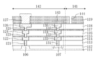
図23は、従来のシールリングを有する半導体装置(ウェハに作り込まれている状態)の断面構造を示している。 FIG. 23 shows a cross-sectional structure of a conventional semiconductor device having a seal ring (in a state of being built in a wafer).
図23に示すように、シリコンウェハよりなる半導体基板111上には、ダイシング領域141によって区画された、ダイシングにより半導体チップとなるチップ領域142が複数設けられている。半導体基板111上には、素子分離膜112、複数(第1〜第6)の層間絶縁膜113〜118及びパッシベーション膜119の積層構造が形成されている。チップ領域142にはトランジスタ等の素子を構成する活性層106が設けられると共に、活性層106は素子分離膜112によって囲まれている。
As shown in FIG. 23, on a
第1の層間絶縁膜113には活性層106と接続する第1のビア121が形成されている。第2の層間絶縁膜114には第1のビア121と接続する第1の配線122が形成されている。第3及び第4の層間絶縁膜115及び116には第1の配線122と接続する第2のビア123が形成されていると共に、第4の層間絶縁膜116には第2のビア123と接続する第2の配線124が形成されている。第5及び第6の層間絶縁膜117及び118には第2の配線124と接続する第3のビア125が形成されていると共に、第6の層間絶縁膜118には第3のビア125と接続する第3の配線126が形成されている。パッシベーション膜119には、第3の配線126と接続するパッド127が形成されている。
A
また、図23に示すように、チップ領域142の周縁部における複数の層間絶縁膜113〜118の積層構造には、該積層構造を貫通し且つチップ領域142を連続的に取り囲むシールリング143が形成されている。シールリング143は、例えば、配線形成用マスクとビア形成用マスクとを交互に用いて形成される。
Further, as shown in FIG. 23, in the laminated structure of the plurality of
具体的には、シールリング143は、半導体基板111に形成された活性層107と、第1の層間絶縁膜113に形成され且つ活性層107と接続する第1のシールビア131と、第2の層間絶縁膜114に形成され且つ第1のシールビア131と接続する第1のシール配線132と、第3及び4の層間絶縁膜115及び116に形成され且つ第1のシール配線132と接続する第2のシールビア133と、第4の層間絶縁膜116に形成され且つ第2のシールビア133と接続する第2のシール配線134と、第5及び6の層間絶縁膜117及び118に形成され且つシール配線134と接続する第3のシールビア135と、第6の層間絶縁膜118に形成され且つ第3のシールビア135と接続する第6のシール配線136とから構成されている。尚、本願においては、シールリングのうち配線形成用マスクによって形成される部分をシール配線、シールリングのうちビア形成用マスクによって形成される部分をシールビアと称する。更に、特許文献1に示すように、パッシベーション膜119にはシールリング143よりもダイシング領域141側に、第6の層間絶縁膜118にまで到達する開口部144が形成されている。
上記に説明した従来の半導体装置は、チップ最表面のパッシベーション膜に開口部が形成されているために、ウェハをダイシングする際に生じたクラックや衝撃がチップ領域へ伝播するのを防止できるという効果を有する。しかし、この効果はパッシベーション膜部のみに限定されている。つまり、パッシベーション膜の下に存在する層間絶縁膜においては、ウェハをダイシングする際に生じたクラックや衝撃が層間絶縁膜を伝播してシールリングに達してしまう。ダイシングの衝撃により、シールリングの一部分に欠損や割れが生じた場合、チップ領域に水分や可動イオン等が侵入することを十分に防止することはできない。 In the conventional semiconductor device described above, since an opening is formed in the passivation film on the outermost surface of the chip, it is possible to prevent propagation of cracks and impacts generated when dicing the wafer to the chip region. Have However, this effect is limited only to the passivation film portion. That is, in the interlayer insulating film existing under the passivation film, cracks and impacts generated when dicing the wafer propagate through the interlayer insulating film and reach the seal ring. In the case where a part of the seal ring is broken or cracked due to the impact of dicing, it is not possible to sufficiently prevent moisture, movable ions, etc. from entering the chip region.
また、シールリングはチップ領域の周縁部に連続的に設けられているため、クラックや衝撃を吸収して破壊されたシールリングの一部が、ダイシングによって個片化された半導体装置(半導体チップ)の端部から飛び出した状態になる場合もある。このような状態の半導体装置に対してパッケージングを行なうと、前記のシールリングの残骸がボンディングワイヤに接触して製品不良となる。 In addition, since the seal ring is continuously provided at the peripheral portion of the chip region, a semiconductor device (semiconductor chip) in which a part of the seal ring broken by absorbing cracks and impacts is separated into pieces by dicing It may be in a state of jumping out from the end of the. When packaging is performed on the semiconductor device in such a state, the residue of the seal ring comes into contact with the bonding wire, resulting in a product defect.
ところで、半導体素子及びそれらと接続する配線の微細化に伴う配線間容量の増大、更にはその結果としての半導体装置の処理速度の低下を防ぐため、比誘電率の低い(低誘電率)シリコン酸化膜などの層間絶縁膜を用いて配線間容量の増大を防止する技術が開発されている。 By the way, in order to prevent the increase in inter-wiring capacitance accompanying the miniaturization of semiconductor elements and wirings connected to them, and the resulting decrease in the processing speed of the semiconductor device, silicon oxide having a low relative dielectric constant (low dielectric constant). A technique for preventing an increase in capacitance between wirings using an interlayer insulating film such as a film has been developed.
しかし、一般的に低誘電率の層間絶縁膜は機械的強度が低いため、低誘電率の層間絶縁膜におけるダイシング時に生じる応力に対する耐性は、従来使用されてきた材料よりなる層間絶縁膜と比べて不十分である。その結果、低誘電率の層間絶縁膜はダイシング時により損傷を受けやすい。従って、ダイシング時におけるクラック等の伝播を防止する機能と、外部からチップ領域内への水分や可動イオン等の進入を防止する機能との両方を、従来のようにシールリングのみによって達成することはますます困難になってきている。 However, since a low dielectric constant interlayer insulating film generally has low mechanical strength, the resistance to stress generated during dicing in a low dielectric constant interlayer insulating film is higher than that of an interlayer insulating film made of a conventionally used material. It is insufficient. As a result, the low dielectric constant interlayer insulating film is more susceptible to damage during dicing. Therefore, it is possible to achieve both the function of preventing the propagation of cracks during dicing and the function of preventing the entry of moisture, movable ions, etc. from the outside into the chip region by using only the seal ring as in the past. It has become increasingly difficult.
前記に鑑み、本発明は、ダイシングによってウェハを個々のチップ(半導体装置)に分割する際に生じるチップ側面の欠けや割れ等がシールリングに到達してシールリングが破壊されるのを防止することによって、該欠けや割れ等が更にチップ領域内に伝播することを防止し、それにより半導体装置の耐湿性及び信頼性の低下を防止することを目的とする。 In view of the above, the present invention prevents chip side cracks or cracks generated when dicing a wafer into individual chips (semiconductor devices) from reaching the seal ring and destroying the seal ring. Therefore, it is an object to prevent the chipping, cracking, and the like from further propagating into the chip region, thereby preventing deterioration of moisture resistance and reliability of the semiconductor device.
前記の目的を達成するため、本発明に係る半導体装置は、基板に形成された素子と、基板上に形成された絶縁膜と、絶縁膜中に、素子の形成された領域を取り囲み且つ絶縁膜を貫通するように形成されたシールリングと、素子から見てシールリングよりも外側に位置する部分の絶縁膜に形成され、少なくとも1つの応力吸収体を含む応力吸収壁と、素子から見て応力吸収壁よりも外側に位置する部分の絶縁膜に形成され、少なくとも1つの空隙を含む空隙領域とを備える。 In order to achieve the above object, a semiconductor device according to the present invention includes an element formed on a substrate, an insulating film formed on the substrate, an insulating film surrounding the region where the element is formed, and the insulating film. A seal ring formed so as to pass through, a stress absorption wall including at least one stress absorber formed on an insulating film located outside the seal ring as viewed from the element, and a stress as viewed from the element A gap region that is formed in a portion of the insulating film located outside the absorption wall and includes at least one gap.
本発明の半導体装置によると、素子から見てシールリングの外側に、少なくとも1つの空隙を含む空隙領域と、少なくとも1つの応力吸収体を含む応力吸収壁とが形成されている。このため、チップ領域を区画するダイシング領域においてウェハをダイシングして個々の半導体装置(半導体チップ)を得る際に、発生するクラックや応力等がシールリングに達するのを空隙領域及び応力吸収壁によって阻止することができる。このため、シールリングに欠損が生じたり、シールリングが破壊されたりするのを防ぐことができ、シールリングは、その本来の機能の一つであるチップ領域の内部を保護する機能を確実に果たすことができる。 According to the semiconductor device of the present invention, the void region including at least one void and the stress absorbing wall including at least one stress absorber are formed outside the seal ring as viewed from the element. For this reason, when the wafer is diced in the dicing area that divides the chip area to obtain individual semiconductor devices (semiconductor chips), the gap area and the stress absorbing wall prevent the generated cracks and stress from reaching the seal ring. can do. For this reason, it is possible to prevent the seal ring from being damaged or broken, and the seal ring reliably performs the function of protecting the inside of the chip region, which is one of its original functions. be able to.
尚、絶縁膜は、複数の層間絶縁膜が積層された構造を有し、複数の層間絶縁膜のうちの少なくとも1つの層間絶縁膜に形成され且つ素子に電気的に接続されたビアと、複数の層間絶縁膜のうちの少なくとも1つの層間絶縁膜に形成され且つ素子に電気的に接続された配線とを備え、シールリングは、ビアが形成された層間絶縁膜に形成されたシールビアと、配線が形成された層間絶縁膜に形成されたシール配線とを含み、応力吸収壁は、少なくとも、複数の層間絶縁膜のうちのシール配線が形成されている層間絶縁膜に形成された応力吸収体を含み、空隙領域は、少なくとも、複数の層間絶縁膜のうちのシール配線が形成されている層間絶縁膜に形成された空隙を含むことが好ましい。 The insulating film has a structure in which a plurality of interlayer insulating films are stacked, a via formed in at least one of the plurality of interlayer insulating films and electrically connected to the element, and a plurality of insulating films And a wiring formed in at least one of the interlayer insulating films and electrically connected to the element, and the seal ring includes a seal via formed in the interlayer insulating film in which the via is formed, and a wiring The stress absorption wall includes at least a stress absorber formed in the interlayer insulating film in which the seal wiring is formed among the plurality of interlayer insulating films. Preferably, the void region includes at least a void formed in the interlayer insulating film in which the seal wiring is formed among the plurality of interlayer insulating films.
シール配線が形成される層間絶縁膜としては、低誘電率絶縁膜を用いることある。一般に、低誘電率絶縁膜は機械的強度が低いため、シール配線が形成されている層間絶縁膜において空隙及び応力吸収体を形成すると、ダイシング時におけるシール配線の損傷及び破壊を防いでチップ領域の内部を保護する効果が顕著に得られる。 A low dielectric constant insulating film may be used as an interlayer insulating film on which a seal wiring is formed. In general, since the low dielectric constant insulating film has low mechanical strength, forming voids and stress absorbers in the interlayer insulating film on which the seal wiring is formed prevents damage and destruction of the seal wiring during dicing and prevents the chip area from being damaged. The effect of protecting the inside is remarkably obtained.
また、ビア及び配線が一体的に形成されたデュアルダマシン配線を含んでいても良い。 Further, dual damascene wiring in which vias and wirings are integrally formed may be included.
ビア及び配線の構成として、このようにすることができる。 Such a configuration of the via and the wiring can be used as described above.
また、配線とビアとは、それぞれ複数の層間絶縁膜のうちの異なる層間絶縁膜中に形成されていても良い。 Further, the wiring and the via may be formed in different interlayer insulating films among the plurality of interlayer insulating films.
また、複数の層間絶縁膜のうちの配線が形成されている層間絶縁膜は、複数の層間絶縁膜のうちのビアが形成されている層間絶縁膜よりも誘電率が低い膜からなることが好ましい。 Further, the interlayer insulating film in which the wiring among the plurality of interlayer insulating films is formed is preferably a film having a lower dielectric constant than the interlayer insulating film in which the via is formed in the plurality of interlayer insulating films. .
このようにすると、配線の形成された層間絶縁膜において配線間の容量を低減することができる。 In this way, the capacitance between the wirings can be reduced in the interlayer insulating film in which the wirings are formed.
また、絶縁膜の上に形成されたパッシベーション膜を更に備え、シールリングは、絶縁膜に加えてパッシベーション膜についても貫通するように形成され、空隙領域は、素子から見てシールリングよりも外側に位置する部分のパッシベーション膜中に形成されているスリットを更に含むことが好ましい。 Further, a passivation film formed on the insulating film is further provided, and the seal ring is formed so as to penetrate the passivation film in addition to the insulating film, and the air gap region is located outside the seal ring as viewed from the element. It is preferable to further include a slit formed in the portion of the passivation film.
このようにすると、パッシベーション膜を含む半導体装置において、パッシベーション膜内を伝わるダイシング時のクラックや応力についても空隙領域によってチップ領域内部方向への伝達を防止することができる。 In this way, in a semiconductor device including a passivation film, it is possible to prevent cracks and stresses during dicing that are transmitted through the passivation film from being transmitted to the inside of the chip region by the gap region.
また、パッシベーション膜は、複数の膜からなる積層構造を有することが好ましい。このようにすると、パッシベーション膜による膜ストレスを緩和することができると共に、一部の膜を低誘電率の膜とすることによって容量を低減することができる。 Further, the passivation film preferably has a laminated structure composed of a plurality of films. Thus, the film stress due to the passivation film can be relieved, and the capacitance can be reduced by making some of the films have low dielectric constants.
また、応力吸収壁は、絶縁膜の厚さ方向に不連続に配置された複数の応力吸収体を含むことが好ましい。このようにすると、より確実に応力又はクラック等を吸収することができる。 The stress absorbing wall preferably includes a plurality of stress absorbers arranged discontinuously in the thickness direction of the insulating film. In this way, stress or cracks can be absorbed more reliably.
また、応力吸収壁は、絶縁膜の厚さ方向に隣接するように配置された複数の応力吸収体を含むことも好ましい。このようにすると、一部の応力吸収体がダイシング時の応力により破壊されたとしても、応力等が伝わって隣の応力吸収体まで破壊されることがない。 The stress absorption wall preferably includes a plurality of stress absorbers arranged so as to be adjacent to each other in the thickness direction of the insulating film. In this way, even if a part of the stress absorber is destroyed by the stress during dicing, the stress or the like is not transmitted to the adjacent stress absorber.
また、配線の形成される層間絶縁膜が誘電率の低い膜からなる場合、このような層間絶縁膜は一般に機械的強度が低いため、ダイシング時の応力やクラックが伝播して破壊されやすい。そこで、低誘電率膜からなる絶縁膜に応力吸収体を選択的に形成することにより、シールリング方向に応力やクラックが伝播するのを効果的に防ぐことができる。 Further, when the interlayer insulating film on which the wiring is formed is made of a film having a low dielectric constant, such an interlayer insulating film generally has a low mechanical strength, so that stress and cracks at the time of dicing propagate and are easily broken. Therefore, by selectively forming a stress absorber in the insulating film made of a low dielectric constant film, it is possible to effectively prevent the propagation of stress and cracks in the seal ring direction.
また、応力吸収壁は、素子から見てシールリングの外側を切れ目無く連続して取り囲むように形成された応力吸収体を含むことが好ましい。 The stress absorbing wall preferably includes a stress absorber formed so as to continuously surround the outer side of the seal ring as viewed from the element.
このようにすると、素子から見てどちらの方向からダイシング時のクラックや応力が伝播して来る場合にも、シールリングへの到達を応力吸収体によって防ぐことができる。 If it does in this way, even if the crack and stress at the time of dicing propagate from which direction seeing from an element, arrival to a seal ring can be prevented by a stress absorber.
また、応力吸収壁は、素子から見てシールリングの外側を不連続に取り囲むように配置された複数の応力吸収体を含むことが好ましい。 Moreover, it is preferable that a stress absorption wall contains the some stress absorber arrange | positioned so that the outer side of a seal ring may be discontinuously enclosed seeing from an element.
このようにすると、ダイシング時のクラック等によって不連続な個々の応力吸収体のいずれかがダメージを受けて破壊されたとしても、破壊がシールリングの延びる方向に沿って拡大することはない。 In this way, even if any of the discontinuous individual stress absorbers is damaged and broken by cracks or the like during dicing, the breakage does not expand along the direction in which the seal ring extends.
また、素子から見て応力吸収壁の外側に、少なくとも1つの応力吸収体を含む少なくとも1つの他の応力吸収壁を更に備えることが好ましい。 In addition, it is preferable to further include at least one other stress absorbing wall including at least one stress absorber outside the stress absorbing wall as viewed from the element.
言い換えると、応力吸収壁及び他の応力吸収壁を合わせて複数の応力吸収壁と呼ぶことにすると、シールリングの外側に2つ以上設けられた応力吸収壁によって、シールリングを2重以上に取り囲んでいることが好ましい。 In other words, when the stress absorbing wall and other stress absorbing walls are collectively referred to as a plurality of stress absorbing walls, two or more stress absorbing walls provided outside the seal ring surround the seal ring more than twice. It is preferable that
このようにすると、クラックや応力がチップ領域の内部方向に侵入するのをより確実に防ぐことができる。つまり、シールリングの外側を2重以上に取り囲む複数の応力吸収壁のうち、ウェハダイシング部分(ダイシング領域のうち実際にダイシング装置のブレードによって切断するための領域)に最も近い位置にある応力吸収壁がダイシング時のクラックや衝撃等を吸収しきれない場合が考えられる。このような場合に、クラックや衝撃等がチップ領域の内部方向へ侵入したとしても、外側の応力吸収壁の内側に少なくとも1つの応力吸収壁が更に形成されている。よって、この内側の応力吸収壁がチップ領域の内部方向へのクラックや衝撃等のさらなる進行を防ぐことができる。 In this way, it is possible to more reliably prevent cracks and stresses from entering the chip region. That is, among the plurality of stress absorbing walls that surround the outside of the seal ring more than twice, the stress absorbing wall that is closest to the wafer dicing portion (the region of the dicing region that is actually cut by the blade of the dicing device). May not be able to absorb cracks and impacts during dicing. In such a case, at least one stress absorbing wall is further formed on the inner side of the outer stress absorbing wall even if a crack, an impact, or the like enters the inside of the chip region. Therefore, this inner stress absorbing wall can prevent further progress such as cracks and shocks in the inner direction of the chip region.
また、他の応力吸収壁は、素子から見てシールリングの外側を切れ目無く連続して取り囲むように形成された応力吸収体を含むことが好ましい。また、他の応力吸収壁は、素子から見てシールリングの外側を不連続に取り囲むように配置された複数の応力吸収体を含むことが好ましい。これらにより、それぞれ、応力吸収壁に関して説明したのと同様の効果が得られる。 Further, the other stress absorbing wall preferably includes a stress absorber formed so as to continuously surround the outside of the seal ring as viewed from the element. The other stress absorbing wall preferably includes a plurality of stress absorbers disposed so as to discontinuously surround the outside of the seal ring as viewed from the element. As a result, the same effects as described for the stress absorbing wall can be obtained.
また、応力吸収壁及び他の応力吸収壁は、それぞれ、素子から見てシールリングの外側を不連続に取り囲むように配置された複数の応力吸収体を含み、応力吸収壁における複数の応力吸収体同士の間の部分と、他の応力吸収壁における複数の応力吸収体の間の部分とは、シールリングの延びる方向に垂直な方向について互いに隣り合わないように配置されていることが好ましい。 Each of the stress absorption wall and the other stress absorption wall includes a plurality of stress absorbers arranged so as to discontinuously surround the outside of the seal ring when viewed from the element, and the plurality of stress absorbers in the stress absorption wall. It is preferable that the portion between them and the portion between the plurality of stress absorbers in the other stress absorbing walls are arranged so as not to be adjacent to each other in the direction perpendicular to the direction in which the seal ring extends.
このようにすると、ダイシング時のクラックや応力等がチップ領域の内側方向に伝達されるのを、2重以上に配置されている複数の応力吸収壁によって確実に防止することができる。これは、外側の応力吸収壁における不連続部分(応力吸収体同士の間の部分)と内側の応力吸収体の不連続部分とがシールリングの延びる方向に対して垂直な方向において互いに隣り合っていないことによる。つまり、クラックや応力等が、ウェハダイシング部分に最も近く配置された応力吸収体によって阻止されず、応力吸収体の不連続部分を通り抜けてチップ領域の内部方向へ侵入したとしても、必ずその内側の他の応力吸収体によって阻止される。 If it does in this way, it can prevent reliably that the crack, stress, etc. at the time of dicing are transmitted to the inner direction of a chip field by a plurality of stress absorption walls arranged more than double. This is because the discontinuous portion (the portion between the stress absorbers) in the outer stress absorbing wall and the discontinuous portion of the inner stress absorber are adjacent to each other in the direction perpendicular to the extending direction of the seal ring. By not. In other words, even if cracks, stresses, etc. are not blocked by the stress absorber disposed closest to the wafer dicing part and pass through the discontinuous part of the stress absorber and invade into the chip area, it must Blocked by other stress absorbers.
言い換えると、ウェハダイシング部分からチップ領域を見た場合には、2重以上にシールリングを取り囲む複数の応力吸収壁における応力吸収体が隙間なく配置されていることになるため、ウェハダイシング部分からチップ領域の内部方向へのクラックや衝撃等の進行を確実に防ぐことができる。よって、ダイシング時のクラックや衝撃等がシールリングに到達する前にそれらを阻止することができるので、シールリングが欠損したり又はシールリングが破壊されることはない。この結果、チップ領域の内部を確実に保護するというシールリングの機能が損なわれるのを防ぐことができる。 In other words, when the chip region is viewed from the wafer dicing portion, the stress absorbers in the plurality of stress absorption walls surrounding the seal ring more than twice are arranged without gaps. It is possible to reliably prevent the progress of cracks and impacts in the internal direction of the region. Therefore, cracks and impacts during dicing can be prevented before reaching the seal ring, so that the seal ring is not lost or broken. As a result, it is possible to prevent the function of the seal ring from reliably protecting the inside of the chip region from being impaired.
また、シールリングを囲むように配置された複数の応力吸収体のうちの少なくとも1つの応力吸収体は、シールリングの延びる方向の寸法が他の応力吸収体とは異なるように形成されていることが好ましい。 Further, at least one of the plurality of stress absorbers arranged so as to surround the seal ring is formed so that the dimension in the extending direction of the seal ring is different from that of the other stress absorbers. Is preferred.
つまり、複数の応力吸収体のシールリングの延びる方向についての寸法が一様ではないように形成されているのがよい。 That is, it is preferable that the dimensions of the plurality of stress absorbers in the extending direction of the seal ring are not uniform.
このようにすると、たとえば衝撃の集中しやすいところには長さの長い応力吸収体を配置し、その他の部分には短い応力吸収体を配置することにより、ダイシング時のクラックや衝撃等を細かく分散して吸収することができる。よって、ダイシング時のクラックや衝撃等がシールリングに到達する前にそれらの侵入を防止できるため、シールリングに欠損が生じたり又はシールリングが破壊されることがない。この結果として、チップ領域の内部を確実に保護するというシールリングの機能が損なわれることがない。 In this way, for example, long stress absorbers are placed where impacts are likely to concentrate, and short stress absorbers are placed elsewhere, so cracks and impacts during dicing are finely dispersed. Can be absorbed. Therefore, since cracks, impacts, and the like during dicing can be prevented from entering before reaching the seal ring, the seal ring is not damaged or broken. As a result, the function of the seal ring that reliably protects the inside of the chip region is not impaired.
また、空隙領域は、絶縁膜の厚さ方向に不連続に配置された複数の空隙を含むことが好ましい。 Moreover, it is preferable that a space | gap area | region contains the several space | gap arrange | positioned discontinuously in the thickness direction of an insulating film.
このようにすると、空隙領域のために半導体装置に構造的強度が低下するのを抑制しながら、ダイシング時のクラックや応力等がシールリングに達するのを防ぐことができる。 In this way, it is possible to prevent cracks, stresses, and the like during dicing from reaching the seal ring while suppressing the structural strength of the semiconductor device from being lowered due to the void region.
また、空隙領域は、絶縁膜の厚さ方向に隣接するように配置された複数の空隙を含むことが好ましい。 Moreover, it is preferable that a space | gap area | region contains the several space | gap arrange | positioned so that it may adjoin in the thickness direction of an insulating film.
このようにすると、絶縁間の厚さ方向について複数の空隙が隣接する範囲について、ダイシング時のクラックや応力等を確実に防ぐことができる。 If it does in this way, the crack, stress, etc. at the time of dicing can be prevented reliably about the range which a several space | gap adjoins about the thickness direction between insulation.
また、空隙領域は、素子から見てシールリングの外側を切れ目無く連続して取り囲むように形成された空隙を含むことが好ましい。 The void region preferably includes a void formed so as to continuously surround the outside of the seal ring as viewed from the element.
このようにすると、素子から見てどちらの方向からダイシング時のクラックや応力が伝播して来る場合にも、シールリングへの到達を空隙領域によって防ぐことができる。 In this way, even when cracks or stress during dicing propagates from either direction as viewed from the element, the gap area can prevent the gap from reaching the seal ring.
また、空隙領域は、素子から見てシールリングの外側を不連続に取り囲むように配置された複数の空隙を含むことが好ましい。 Moreover, it is preferable that a space | gap area | region contains several space | gap arrange | positioned so that the outer side of a seal ring may be discontinuously enclosed seeing from an element.
このようにすると、耐衝撃性の低い箇所等について選択的に空隙を形成し、特にそのような箇所に関してクラックや応力の伝達を防ぐことができる。 If it does in this way, a space | gap can be selectively formed about a location with low impact resistance, etc., and the transmission of a crack and stress can be prevented especially regarding such a location.
また、素子から見て前記空隙領域の外側に、少なくとも1つの空隙を含む少なくとも1つの他の空隙領域を更に備えることが好ましい。 In addition, it is preferable to further include at least one other void region including at least one void outside the void region when viewed from the element.
言い換えると、空隙領域及び他の空隙領域を合わせて複数の空隙領域と呼ぶことにすると、シールリングの外側に2つ以上設けられた空隙領域によって、シールリングを2重以上に取り囲んでいることが好ましい。これにより、応力吸収壁と他の応力吸収壁とを備える場合と同様の理由から、クラックや応力がチップ領域の内部方向に侵入するのをより確実に防ぐことができる。 In other words, if the gap area and other gap areas are collectively referred to as a plurality of gap areas, the seal ring may be surrounded more than once by two or more gap areas provided outside the seal ring. preferable. Thereby, for the same reason as the case where the stress absorbing wall and other stress absorbing walls are provided, it is possible to more reliably prevent cracks and stress from entering the inside of the chip region.
また、他の空隙領域は、素子から見てシールリングの外側を切れ目無く連続して取り囲むように形成された空隙を含むことが好ましい。また、他の空隙領域は、素子から見てシールリングの外側を不連続に取り囲むように配置された複数の空隙を含むことも好ましい。これらにより、それぞれ、空隙領域に関して説明したのと同様の効果が得られる。 Further, it is preferable that the other void region includes a void formed so as to continuously surround the outside of the seal ring as viewed from the element. It is also preferable that the other void region includes a plurality of voids disposed so as to discontinuously surround the outside of the seal ring when viewed from the element. As a result, the same effects as described for the void region can be obtained.
また、空隙領域及び他の空隙領域は、それぞれ、素子から見てシールリングの外側を不連続に取り囲むように配置された複数の空隙を含み、空隙領域における複数の空隙同士の間の部分と、他の空隙領域における複数の空隙の間の部分とは、シールリングの延びる方向に垂直な方向について互いに隣り合わないように配置されていることが好ましい。 In addition, each of the void region and the other void region includes a plurality of voids disposed so as to discontinuously surround the outside of the seal ring when viewed from the element, and a portion between the plurality of voids in the void region; It is preferable that portions between the plurality of gaps in the other gap regions are arranged so as not to be adjacent to each other in the direction perpendicular to the extending direction of the seal ring.
また、シールリングを囲むように配置された複数の空隙のうちの少なくとも1つの空隙は、シールリングの延びる方向の寸法が他の空隙とは異なるように形成されていることが好ましい。 Moreover, it is preferable that at least one of the plurality of gaps arranged so as to surround the seal ring is formed so that the dimension in the extending direction of the seal ring is different from that of the other gaps.
これらのことにより、やはり応力吸収壁と他の応力吸収壁とを備える場合と同様の理由から、クラックや応力がチップ領域の内部方向に侵入するのをより確実に防ぐことができる。 For these reasons, it is possible to more reliably prevent cracks and stress from entering the inside of the chip region for the same reason as when the stress absorbing wall and other stress absorbing walls are provided.
前記の目的を達成するため、本発明の第1の半導体装置の製造方法は、基板上に素子を形成する工程と、素子を形成した基板上に、層間絶縁膜を形成する工程と、層間絶縁膜に、素子に電気的に接続する配線及びビアの少なくとも一方を形成するための第1の凹部と、第1の凹部を取り囲み且つシールリングの少なくとも一部を形成するための第2の凹部と、素子から見て第2の凹部の外側に応力吸収体を形成するための第3の凹部と、素子から見て第2の凹部の外側に空隙を形成するための第4の凹部とを形成する工程と、第1の凹部と第2の凹部と第3の凹部とに導電膜を埋め込むことにより、配線及びビアの少なくとも一方とシールリングの少なくとも一部と応力吸収体を形成すると共に、第4の凹部を空隙として残す工程とを備える。 In order to achieve the above object, a first method of manufacturing a semiconductor device according to the present invention includes a step of forming an element on a substrate, a step of forming an interlayer insulating film on the substrate on which the element is formed, and an interlayer insulation. A first recess for forming at least one of a wiring and a via electrically connected to the element in the film; and a second recess for surrounding the first recess and forming at least a part of the seal ring; Forming a third recess for forming a stress absorber outside the second recess as viewed from the element and a fourth recess for forming a gap outside the second recess as viewed from the element And embedding a conductive film in the first recess, the second recess, and the third recess to form at least one of the wiring and via, at least a part of the seal ring, and a stress absorber. And a step of leaving the four concave portions as voids.
第1の半導体装置の製造方法によると、半導体基板上に形成された素子に電気的に接続されたビア及び配線をシールリングが取り囲み、その外側に応力吸収体及び空隙が形成された半導体装置を製造することができる。これにより製造される半導体装置は、既に説明した本発明の半導体装置の効果を有する。 According to the first method for manufacturing a semiconductor device, a semiconductor device in which a seal ring surrounds a via and a wiring electrically connected to an element formed on a semiconductor substrate and a stress absorber and a gap are formed outside the seal ring. Can be manufactured. The semiconductor device manufactured thereby has the effect of the semiconductor device of the present invention already described.
尚、第1の凹部に、ビア及び前記配線を、デュアルダマシン法によって一体的に形成しても良い。 Note that the via and the wiring may be integrally formed in the first recess by a dual damascene method.
前記の目的を達成するため、本発明の第2の半導体装置の製造方法は、基板上に素子を形成する工程と、素子を形成した基板上に、層間絶縁膜を形成する工程と、層間絶縁膜に、素子に電気的に接続する配線及びビアの少なくとも一方を形成するための第1の凹部と、第1の凹部を取り囲み且つシールリングの少なくとも一部を形成するための第2の凹部と、素子から見て第2の凹部の外側に応力吸収体を形成するための少なくとも2つの第3の凹部とを形成する工程と、第1の凹部と第2の凹部と第3の凹部とに導電膜を埋め込むことにより、配線及びビアの少なくとも一方とシールリングの少なくとも一部と応力吸収体を形成する工程と、応力吸収体に挟まれた部分において層間絶縁膜を除去することにより空隙を形成する工程とを備え、少なくとも2つの第3の凹部は、素子から見て外側に向かう方向に並んでいる。 In order to achieve the above object, a second method of manufacturing a semiconductor device according to the present invention includes a step of forming an element on a substrate, a step of forming an interlayer insulating film on the substrate on which the element is formed, and an interlayer insulation. A first recess for forming at least one of a wiring and a via electrically connected to the element in the film; and a second recess for surrounding the first recess and forming at least a part of the seal ring; A step of forming at least two third recesses for forming a stress absorber outside the second recess as viewed from the element, and a first recess, a second recess, and a third recess. A step of forming a stress absorber by embedding a conductive film and forming at least one of a wiring and a via, at least a part of a seal ring, and a portion sandwiched between stress absorbers to form a gap And the process of At least two third recesses are arranged in the direction toward the outside as viewed from the element.
このような第2の製造方法によっても、本発明に係る半導体装置を製造することができる。 The semiconductor device according to the present invention can be manufactured also by such a second manufacturing method.
以上に説明したように、本発明によると、半導体基板上に形成された素子と、該素子が形成されたチップ領域の周縁部に設けられ且つ素子や配線層等の周囲を囲むシールリングとを備えた半導体装置において、シールリングを取り囲むように、少なくとも1つの応力吸収体を含む応力吸収壁と少なくとも1つの空隙を含む空隙領域とが設けられている。また、このような応力吸収体、空隙は連続した構造あるいは不連続に形成されていてもよく、複数の空隙領域を設けてシールリングの外側を2重以上に取り囲む構造としてもよい。特に、2重以上で且つ不連続に形成される場合、それぞれにおける不連続部分は互いに隣り合わないことが好ましい。 As described above, according to the present invention, an element formed on a semiconductor substrate, and a seal ring that is provided at a peripheral portion of a chip region where the element is formed and surrounds the periphery of the element, the wiring layer, and the like. In the provided semiconductor device, a stress absorption wall including at least one stress absorber and a void region including at least one void are provided so as to surround the seal ring. Further, such stress absorbers and voids may be formed in a continuous structure or discontinuously, and a plurality of void regions may be provided so as to surround the outside of the seal ring more than twice. In particular, in the case where the layers are formed more than twice and discontinuously, it is preferable that the discontinuous portions in each are not adjacent to each other.
前述の本発明の特徴によって、ウェハから個々のチップ(半導体装置)を取り出す際のダイシングによって生じるウェハの欠けや割れ等がシールリングに至る前にそれらを1重又は2重以上の応力吸収体及び空隙によって阻止することができるため、シールリングの破壊、ひいては半導体装置となるチップ領域の破壊を防ぐことができ、それによって半導体チップの耐湿性及び信頼性の低下を防止することができる。 According to the above-described feature of the present invention, before the chip or crack of the wafer caused by dicing when taking out individual chips (semiconductor devices) from the wafer reaches the seal ring, the single or double stress absorbers and Since it can be blocked by the air gap, it is possible to prevent the seal ring from being broken, and hence the chip region that becomes the semiconductor device, and thereby the deterioration of moisture resistance and reliability of the semiconductor chip can be prevented.
(第1の実施形態)
以下、本発明の第1の実施形態に係る半導体装置及びその製造方法について図面を参照しながら説明する。
(First embodiment)
Hereinafter, a semiconductor device and a manufacturing method thereof according to a first embodiment of the present invention will be described with reference to the drawings.
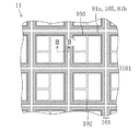
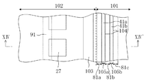
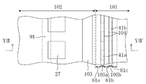
図1は、本発明の第1の実施形態に係る半導体装置が設けられているウェハの一部分を示す平面図である。 FIG. 1 is a plan view showing a part of a wafer provided with a semiconductor device according to the first embodiment of the present invention.
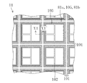
図1に示すように、例えばシリコン基板等に代表される半導体基板11となるウェハ上には、それぞれ半導体装置となる複数のチップ領域102が配置されている。各チップ領域102には、複数の素子からなり且つ所定の機能を有するIC(integrated circuit)回路が設けられている。尚、各チップ領域102は、格子状に設けられたダイシング領域101によって区画されている。
As shown in FIG. 1, a plurality of
ここで、1個の半導体装置(つまり、1個の半導体チップ)は、複数の素子からなり且つ所定の機能を有するIC回路が配置されているチップ領域102と、チップ領域102の周縁部に該チップ領域102を取り囲むように設けられているシールリング103と、シールリング103の外側にシールリング103を取り囲むように設けられている本発明の応力吸収壁81a及び81bと、空隙領域105とを含む構成である。このように複数の半導体装置が形成された半導体ウェハは、各チップの完成後、ダイシング領域101に沿ってダイシングされ、それによって個々の半導体装置に分離される。
Here, one semiconductor device (that is, one semiconductor chip) includes a
応力吸収壁81a及び81bと、空隙領域105とは、ダイシング時にシールリング103が受ける衝撃や応力等を軽減するために設けられている。このため、ダイシングを、シールリング103が存在する側から見て応力吸収壁81a及び81bと、空隙領域105とよりも外側で行われなければならないのは当然のことである。
The
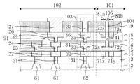
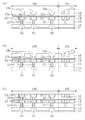
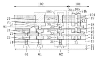
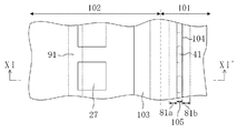
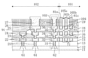
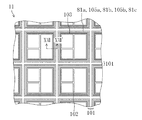
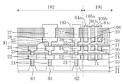
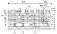
次に、図2は、図1のII-II'線による断面図である。つまり、チップ領域102の周縁部に位置するシールリング103、応力吸収壁81a、応力吸収壁81b及び空隙領域105を含む半導体装置端部(具体的には、チップ領域102の配線構造、シールリング103の構造、応力吸収壁81a、応力吸収壁81b及び空隙領域105)の断面図である。また、図3は、図1のII-II'線の近傍を拡大した平面図である。
Next, FIG. 2 is a cross-sectional view taken along the line II-II ′ of FIG. That is, the semiconductor device end including the
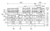
図2及び図3に示すように、ダイシング前の半導体装置はダイシング領域101とチップ領域102とを含む構成である。半導体基板11(以下、基板11と称する)上には、素子分離膜12、絶縁膜(第1〜第6の層間絶縁膜13〜18)及びパッシベーション膜19が形成されている。また、絶縁膜中に、チップ領域102におけるダイシング領域101との境界付近に、第1、第2及び第3のシールビア31、33及び35と、第1、第2及び第3のシール配線32、34及び36とを含むシールリング103が形成されている。これと共に、該シールリング103の外側(ダイシング領域101におけるチップ領域102との境界付近)に、第1、第2及び第3の応力吸収体71x、72x及び73xを含む応力吸収壁81aと、同様に第1、第2及び第3の応力吸収体71y、72y及び73yを含む応力吸収壁81bと、第1の空隙41を含む空隙領域105とが形成されている。尚、2つの応力吸収壁81a及び応力吸収壁81bの間に空隙領域105が配置されている。
As shown in FIGS. 2 and 3, the semiconductor device before dicing has a configuration including a
更に、チップ領域102のシールリング103よりも内側の部分には、第1、第2及び第3のビア21、23及び25と第1、第2及び第3の配線22、24及び26とを含む配線構造と、第1及び第2のビア、第1及び第2の配線を含む他の配線構造とが形成されている。配線構造及び他の配線構造における第2の配線同士の間には、配線間空隙91が設けられている。パッシベーション膜19中に、第3の配線26上にはパッド27、第3のシール配線36上にはキャップ37が形成されている。
Further, the first, second, and
以下、図2及び図3に示す構造を有する半導体装置の製造方法について、対応する図面を参照しながら説明する。尚、以下の説明では、図2に示す第1の応力吸収体71x及び71yをまとめて第1の応力吸収体71と呼ぶ。同様に、第2の応力吸収体72x及び72y、第3の応力吸収体73x及び73yをそれぞれまとめて第2の応力吸収体72、第3の応力吸収体73と呼ぶ。各図においてもこのように符号を付ける。
Hereinafter, a method for manufacturing a semiconductor device having the structure shown in FIGS. 2 and 3 will be described with reference to the corresponding drawings. In the following description, the
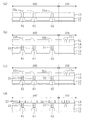
まず、図4(a)に示すように、半導体基板11上に素子分離膜12を形成し、チップ領域102に、トランジスタ等の素子を構成する活性層61を(図4(a)の例では2つ)形成すると共に、基板11におけるチップ領域102の周縁部(ダイシング領域101の近傍のシールリング形成領域)に、活性層と同様に構成された活性層62を形成する。
First, as shown in FIG. 4A, an
次に、基板11上に第1の層間絶縁膜13を堆積する。この後、リソグラフィー法及びドライエッチング法を用いて、チップ領域102の第1の層間絶縁膜13に、それぞれの活性層61上に第1のビア21を形成するためのビアホール21aを形成する。これと共に、シールリング形成領域の第1の層間絶縁膜13に、活性層62上に第1のシールビア31を形成するための第1のシールビアホール31aを形成する。ここで、シールビアとは、シールリングを構成するパーツであって、チップ領域を連続的に取り囲む溝部に導電材料を埋め込むことによって形成される。つまり、シールビアは、チップ領域のビアと同程度の幅を有するライン状構造を有する。
Next, a first
尚、本実施形態において、チップ領域102の第1の層間絶縁膜13にビアホール21aを形成する際に、第1のシールビア31を形成するためのシールビアホール31aを同時に形成したが、ビアホール21aとシールビアホール31aを別々に形成してもよい。
In this embodiment, when the via
次に、図4(b)に示す工程を行なう。まず、第1のビアホール21a及び第1のシールビアホール31aに、Ti又はTiN等のバリアメタルを形成する。この後、W等の金属を埋め込み、CMP(Chemical Mechanical Polishing )法を用いて余分なバリアメタル及び金属を除去し、それぞれ第1のビア21及び第1のシールビア31を形成する。
Next, the process shown in FIG. First, a barrier metal such as Ti or TiN is formed in the first via
次に、第1の層間絶縁膜13上に第2の層間絶縁膜14を形成する。更に、リソグラフィー法を用いて、第2の層間絶縁膜14に配線溝を形成するための配線溝パターン22b、シール配線溝を形成するためのシール配線溝パターン32b及び第1の応力吸収体71を形成するための第1の応力吸収体形成用パターン71bを有するレジスト51を形成する。ここで、シール配線とは、シールリング103を構成するパーツであって、チップ領域102を連続的に取り囲む溝部(第1のシール配線溝32a等)に導電材料を埋め込むことによって形成される。
Next, a second
次に、図4(c)に示すように、ドライエッチング法を用いて、チップ領域102の第2の層間絶縁膜14に、それぞれ第1のビア21と接続するように、第1の配線22を形成するための第1の配線溝22aを形成する。これと共に、シールリング形成領域の第2の層間絶縁膜14に、第1のシールビア31と接続するように、第1のシール配線32を形成するための第1のシール配線溝32aを形成する。更に、ダイシング領域101の第2の層間絶縁膜14に、第1の応力吸収体71を形成するための第1の応力吸収体形成用溝71aを形成する。それぞれが応力吸収体を有する2つの応力吸収壁81a及び81bを設けるために、図4(c)においても2つの第1の応力吸収体形成用溝71aを設けることが示されている。
Next, as shown in FIG. 4C, the
次に、図4(d)に示す工程を行なう。まず、第1の配線溝22a、第1のシール配線溝32a及び第1の応力吸収体形成用溝71aに、Ta、TaN等のバリアメタルをスパッタ法にて形成した後、Cuからなる金属膜をメッキ法にて形成し、更に、第1の配線溝22a、第1のシール配線溝32a及び第1の応力吸収体形成用溝71aからはみ出した部分のバリアメタル及びCuをCMP法にて除去する。これにより、チップ領域102の第2の層間絶縁膜14中に、第1の配線22及び第1のシール配線32が形成される。また、同時に、ダイシング領域101の第2の層間絶縁膜14中に、第1の応力吸収体71が形成される。
Next, the process shown in FIG. First, a barrier metal such as Ta or TaN is formed by sputtering in the
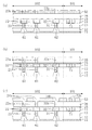
次に、図5(a)に示すように、第2の層間絶縁膜14上に第3の層間絶縁膜15及び第4の層間絶縁膜16を順に形成する。更に、リソグラフィー法を用いて、第4の層間絶縁膜16に第2のビアホール23aを形成するための第2のビアホールパターン23bと、第2のシールビアホール33aを形成するための第2のシールビアパターン33bとを有するビアパターン形成用レジスト52を形成する。
Next, as shown in FIG. 5A, a third
次に、図5(b)に示すように、ドライエッチング法を用いて、チップ領域102の第4の層間絶縁膜16に、第1の配線22と接続する第2のビア23を形成するための第2のビアホール23aを形成する。これと共に、シールリング形成領域の第4の層間絶縁膜16に、第1のシール配線32と接続する第2のシールビア33を形成するための第2のシールビアホール33aを形成する。この後、アッシング及び洗浄を行ない、ビアパターン形成用レジスト52を除去する。
Next, as shown in FIG. 5B, the second via 23 connected to the
次に、図5(c)に示すように、第4の層間絶縁膜16上に、レジスト53を形成する。レジスト53には、リソグラフィー法を用いて、第4の層間絶縁膜16に第2の配線溝24aを形成するための第2の配線溝パターン24b、第2のシール配線溝34aを形成するための第2のシール配線溝パターン34b及び第2の応力吸収体形成用溝72aを形成するための第2の応力吸収体形成用パターン72bを設ける。
Next, as shown in FIG. 5C, a resist 53 is formed on the fourth
次に、図6(a)に示す工程を行なう。ここでは、ドライエッチング法を用いて、チップ領域102の第4の層間絶縁膜16に、第2の配線24を形成するための第2の配線溝24aをビアホール23aと接続するように形成する。これと共に、シールリング形成領域の第4の層間絶縁膜16に、第2のシール配線34を形成するための第2のシール配線溝34aを第2のシールビア33と接続するように形成する。更に、ダイシング領域101の第4の層間絶縁膜16に、第2の応力吸収体72を形成するための第2の応力吸収体形成用溝72aを形成する。この後、アッシング及び洗浄を行ない、レジスト53を除去する。
Next, the process shown in FIG. Here, the
次に、図6(b)に示すように、ドライエッチング法を用いて第1の配線22及び第1のシール配線32上の部分の第3の層間絶縁膜15を除去する。これにより、第2のビアホール23a及び第2のシールビアホール33a内に、それぞれ、第1の配線22及び第1のシール配線32の上部を露出させる。
Next, as shown in FIG. 6B, the portion of the third
次に、図6(c)の工程を行なう。ここでは、第2のビアホール23a及び第2の配線溝24aと、第2のシールビアホール33a及び第2のシール配線溝34aと、第2の応力吸収体形成用溝72aとに、Ta、TaN等からなるバリアメタルをスパッタ法にて形成した後、Cuからなる金属膜をメッキ法にて形成する。その後、はみ出した部分のバリアメタル及びCuをCMP法で除去して、チップ領域102の第4の層間絶縁膜16中に、第2のビア23、第2の配線24、第2のシールビア33及び第2のシール配線34を形成する。同時に、ダイシング領域101の第4の層間絶縁膜16中に、第2の応力吸収体72を形成する。尚、ここではビアホールと配線溝とを同時に金属によって埋め込むデュアルダマシン法を用いて、ビア、配線、シールビア及びシール配線を形成している。
Next, the process of FIG. 6C is performed. Here, the second via
次に、図7(a)に示す工程を行う。まず、第4の層間絶縁膜16上に、第2の配線24、第2のシール配線34及び第2の応力吸収体72上を覆うように、第5の層間絶縁膜17を形成する。更に、第5の層間絶縁膜上に、リソグラフィー法を用いて、レジスト54を形成する。このとき、レジスト54に、第5の層間絶縁膜17における第2の配線24同士の間に配線間空隙形成領域91aを形成するための配線間空隙形成用溝91bと、第2の応力吸収体72同士の間に第1の空隙形成用溝41aを形成するための空隙形成用溝41bとを設ける。
Next, the process shown in FIG. First, the fifth
次に、図7(b)に示す工程を行う。ここでは、レジスト54をマスクとして第4の層間絶縁膜16及び第5の層間絶縁膜17に対してドライエッチングを行い、配線間空隙形成領域91aと第1の空隙形成用溝41aとをそれぞれの位置に設ける。この後、アッシング及び洗浄を行ってレジスト54を除去する。
Next, the process shown in FIG. Here, dry etching is performed on the fourth
次に、図7(c)に示すように、第5の層間絶縁膜17上に例えばCDV法を用いて第6の層間絶縁膜18を形成する。この結果、配線間空隙形成領域91a及び第1の空隙形成用溝41bには第6の層間絶縁膜18が入り込まず、配線間空隙91と第1の空隙41とが形成される。
Next, as shown in FIG. 7C, a sixth
次に、図8(a)に示すように、第6の層間絶縁膜18の表面を平坦化する。
Next, as shown in FIG. 8A, the surface of the sixth
次に、図5(a)〜(c)、図6(a)〜(c)に示したのと同様の工程を繰り返すことにより、図8(b)の構造を得る。具体的には、チップ領域102において、第2の配線24のうちの一方に接続するように、第5及び第6の層間絶縁膜17及び18中に第3のビア25、該第3のビア25に接続するように第6の層間絶縁膜18中に第3の配線を形成する。また、シールリング形成領域において、第5及び第6の層間絶縁膜17及び18中に第3のシールビア35、第6の層間絶縁膜18中に第3のシール配線36を形成する。更に、ダイシング領域において、第6の層間絶縁膜18中に第3の応力吸収体73を形成する。
Next, by repeating the same steps as shown in FIGS. 5A to 5C and FIGS. 6A to 6C, the structure of FIG. 8B is obtained. Specifically, in the
次に、図8(c)に示す工程を行なう。まず、本実施形態の例において最も上に位置する配線層となる第6の層間絶縁膜18上に、該配線層の保護膜となるパッシベーション膜19を形成する。続いて、リソグラフィー法を用い、パッシベーション膜19にパッド開口部27aを形成するためのパッド溝パターン27b、シールリング上部にキャップ溝37aを形成するためのキャップ溝形成パターン37b、及び、スリット104を形成するためのスリット形成パターン104aを有するパッシベーション膜加工用レジスト55を形成する。
Next, the process shown in FIG. First, a
次に、図9(a)に示すように、ドライエッチング法を用いて、チップ領域102のパッシベーション膜19に、第3の配線26と接続するパッド27を形成するためのパッド溝27aを形成する。これと共に、シールリング形成領域のパッシベーション膜19において、第3のシール配線36と接続するキャップ37を形成するためのキャップ溝37aを形成する。更に、ダイシング領域101のパッシベーション膜19に、スリット104を形成する。この後、アッシング及び洗浄を行ない、レジスト55を除去する。
Next, as shown in FIG. 9A, a
次に、図9(b)の工程を行なう。ここでは、パッド溝27aと、キャップ溝37aとに、Ti、TiN等からなるバリアメタル及びAl等の金属膜を順に形成した後、リソグラフィー法及びドライエッチング法によりバリアメタル及び金属膜をパターン化し、パッド27及びキャップ37を形成する。スリット104については、何も埋め込むことなく残す。
Next, the process of FIG. 9B is performed. Here, after a barrier metal made of Ti, TiN or the like and a metal film of Al or the like are sequentially formed in the
以上の工程により、基板11(ウェハ)上における複数の半導体装置の形成が完了する。このようにして半導体装置の製造方法によると、チップ領域102の第1、第2及び第3のビア21、23及び25と、第1、第2及び第3の配線22、24及び26と、パッド27とをそれぞれ形成するのと同時に、順に、第1、第2及び第3のシールビア31、33及び35と、第1、第2及び第3のシール配線32、34及び36と、キャップ37とをそれぞれ形成し、シールリング103を構成することができる。更に、シールリング103の外側に、第1、第2及び第3の応力吸収体71、72及び73をそれぞれ含む応力吸収壁81a及び81bと、これらの間に位置し且つ第1の空隙41を含む空隙領域105とを形成することができる。
Through the above steps, formation of a plurality of semiconductor devices on the substrate 11 (wafer) is completed. Thus, according to the method for manufacturing a semiconductor device, the first, second, and
本実施形態に係る半導体装置は、次のような効果を有する。 The semiconductor device according to the present embodiment has the following effects.
複数の半導体装置が形成されたウェハである基板11は、ダイシング領域101(図1を参照)に沿ってダイシングを行なうことにより、個々の半導体装置(半導体チップ)に分離される。このとき、ダイシングされる部分から、衝撃若しくは応力等又はそれらに起因するクラックが発生し、チップ領域102方向へ伝播する。しかし、このような衝撃、応力、クラック等は、応力吸収壁81a及び81bと、空隙領域105とによって吸収される。言い換えると、衝撃、応力又はクラック等のチップ領域102方向へのさらなる伝播が阻止される。これにより、シールリング103がダメージを受けることがなくなるので、シールリングの本来の機能の1つである、チップ領域102内に外部から水分や可動イオン等が侵入することを防ぐ機能が保たれる。そのため、信頼性の高い半導体装置となっている。
A
尚、絶縁膜中に設けた空隙は、半導体装置の構造的な強度を低下させる原因となりうる。しかし、本実施形態の半導体装置の場合、空隙41と並ぶように応力吸収体72を設けていることにより、空隙のみを設けている場合に比べて構造的な強度を向上させている。
Note that the voids provided in the insulating film can cause a reduction in the structural strength of the semiconductor device. However, in the case of the semiconductor device according to the present embodiment, the structural strength is improved by providing the
また、チップ領域102の側から見て応力吸収壁81a、空隙領域105、応力吸収壁81bと並んでおり、空隙41は2つの応力吸収体72の間に位置している。このため、ダイシングの際のクラックや応力が外側(応力吸収壁81b)の応力吸収体72を破壊したとしても、空隙41の部分において膜の連続性が途切れているためにクラックや応力の伝播が阻止される。このため、内側(応力吸収壁81a)の応力吸収体72は破壊されず、また、シールリング103を保護することができる。
Further, when viewed from the
これらの点は、後に説明する第2〜第4の実施形態の場合にも共通して言えることである。 These points are also true in the case of the second to fourth embodiments described later.
但し、シールリングの外側に、空隙及び応力吸収体が間に層間絶縁膜を挟んで並んでいるような構造であってもよい。少なくとも1つずつの空隙及び応力吸収体を備える構造であれば、クラックや応力の伝播を阻止してシールリングの破壊を防ぐという本実施形態の半導体装置の効果は実現される。更に、チップ領域102の側から見て空隙及び応力吸収体のどちらが内側に配置されているのであっても良い。
However, a structure in which voids and stress absorbers are arranged outside the seal ring with an interlayer insulating film interposed therebetween may be employed. If the structure is provided with at least one gap and a stress absorber, the effect of the semiconductor device of this embodiment that prevents the propagation of cracks and stress and prevents the seal ring from being destroyed is realized. Further, either the air gap or the stress absorber may be disposed inside as viewed from the
また、第1の実施形態に係る半導体装置において、配線(22、24、26)及びシール配線(32、34、36)を確実に保護するために、シール配線を囲むように応力吸収体(71、72、73)又は空隙41が形成されている。配線同士の誘電率を下げるために、配線が形成されている層には低誘電率絶縁膜が使用されることが多い。そのため、空隙領域105を設けることの効果を発揮するためには、配線が形成されているレベルに設けられているシール配線を確実に保護することが重要である。このことから、ビア(21、23、25)及びシールビア(31、33、35)が形成されているレベルにのみ応力吸収体又は空隙が形成されている場合と比較して、配線及びシール配線が形成されているレベルに応力吸収体又は空隙が形成されている場合の方が、ダイシング時の衝撃を吸収する点で望ましい。このことについても、後に説明する第2〜第4の実施形態の場合にも共通して言えることである。尚、ここで言う「レベル」とは、ビア、シールビア、配線、シール配線のそれぞれにおける下面の高さから上面の高さまでの範囲に含まれる空間を指している。
In the semiconductor device according to the first embodiment, the stress absorber (71) surrounds the seal wiring in order to securely protect the wiring (22, 24, 26) and the seal wiring (32, 34, 36). 72, 73) or the
また、本実施形態では、第2の応力吸収体72同士(図2においては72x及び72yと符号を付している)の間の部分の第4の層間絶縁膜16を除去することにより第1の空隙41を形成した(図7(a)〜(c)等を参照)。しかし、このような方法には限られない。例えば、図6(a)に示す工程にて第2の応力吸収体形成用溝72aを形成する際に、加えて空隙を形成するための溝を形成しておき、該溝にはバリアメタル及び配線材料を埋め込まないようにすることにより空隙を設けても良い。このためには、例えば空隙形成用の溝を第2の応力吸収体形成用溝72aよりも狭くする。このようにすると、空隙形成用の溝にはバリアメタルが部分的にしか形成されないか、又は、その開口部が閉塞されるようになり、配線材料が埋め込まれなくなくなる。
In the present embodiment, the first
(第2の実施形態)
以下、本発明の第2の実施形態に係る半導体装置及びその製造方法について、図面を参照しながら説明する。
(Second Embodiment)
Hereinafter, a semiconductor device and a manufacturing method thereof according to a second embodiment of the present invention will be described with reference to the drawings.
図10は、本発明の第2の実施形態に係る半導体装置が設けられているウェハの一部分を示す平面図である。これは、第1の実施形態における図1と同様であるから、詳しい説明は省略する。 FIG. 10 is a plan view showing a part of a wafer provided with a semiconductor device according to the second embodiment of the present invention. Since this is the same as FIG. 1 in the first embodiment, a detailed description thereof will be omitted.
次に、図11は、図10のXI-XI'線による断面図である。つまり、チップ領域102の周縁部に位置するシールリング103、応力吸収壁81a、応力吸収壁81b及び空隙領域105を含む半導体装置端部(具体的には、チップ領域102の配線構造、シールリング103の構造、応力吸収壁81a、応力吸収壁81b及び空隙領域105)の断面図である。また図12は、図10のXI-XI'線の近傍を拡大した平面図である。
Next, FIG. 11 is a cross-sectional view taken along the line XI-XI ′ of FIG. That is, the semiconductor device end including the
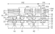
図10〜図12に示すように、ダイシング前の半導体装置はダイシング領域101とチップ領域102とを含む構成である。チップ領域102におけるダイシング領域101との境界付近にシールリング103が形成されている。これと共に、該シールリング103の外側(ダイシング領域101におけるチップ領域102との境界付近)には、シールリング103と平行に不連続に配置された複数の空隙41を含む空隙領域105が形成されている。
As shown in FIGS. 10 to 12, the semiconductor device before dicing has a configuration including a
以上に説明したように、第2の実施形態に係る半導体装置は、シールリング103の外側に、シールリング103と平行に形成されている空隙領域105に含まれる複数の空隙が長さ方向に不連続に配置されている外は、第1の実施形態に係る半導体装置と同じ構造である。また、第2の実施形態に係る半導体装置の製造方法は、空隙形成用溝パターンを形成するためのリソグラフィー用マスクを変更するのみで、図4(a)〜(d)、図5(a)〜(c)、図6(a)〜(c)、図7(a)〜(c)、図8(a)〜(c)、図9(a)及び(b)を用いて説明した第1の実施形態に係る半導体装置の製造方法と同じ方法を用いることができる。
As described above, in the semiconductor device according to the second embodiment, a plurality of voids included in the
本発明の第2の実施形態に係る半導体装置によると以下のような効果がある。つまり、半導体装置が形成されたウェハである基板11は、ダイシング領域101に沿ってダイシングを行なうことによって、個々の半導体装置(半導体チップ)に分離される。このとき、ダイシングされる部分から衝撃若しくは応力等又はそれらに起因するクラックが発生し、チップ領域102方向へ伝播する。しかし、これらの衝撃、応力又はクラック等は不連続に配置された空隙によって細かく分散して吸収できる。また応力の集中しやすいところに選択的に空隙を配置すること、空隙の長さを変化させることもできる。その結果、ダイシング時に発生するクラックや応力を吸収したり、チップ方向への伝播を防止することができる。以上のように、シールリング103がダメージを受けることがなくなるので、シールリングの本来の機能の1つである、チップ領域102内に外部から水分や可動イオン等が侵入することを防ぐ機能が保たれ、それによって信頼性の高い半導体装置を製造することができる。
The semiconductor device according to the second embodiment of the present invention has the following effects. That is, the
(第3の実施形態)
以下、本発明の第3の実施形態に係る半導体装置及びその製造方法について図面を参照しながら説明する。
(Third embodiment)
Hereinafter, a semiconductor device and a manufacturing method thereof according to a third embodiment of the present invention will be described with reference to the drawings.
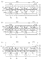
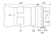
図13は、本発明の第3の実施形態に係る半導体装置が設けられているウェハの一部分を示す平面図である。これは、第1の実施形態における図1と同様である。但し、本実施形態の場合にはシールリング103の外側に3つの応力吸収壁81a、81b及び81cと、2つの空隙領域105a及び105bとを備えていることが示されている。尚、更に多くの応力吸収壁及び空隙領域を備えることも可能である。
FIG. 13 is a plan view showing a part of a wafer provided with a semiconductor device according to the third embodiment of the present invention. This is the same as FIG. 1 in the first embodiment. However, in the case of the present embodiment, it is shown that three
次に図14は、図12のXIV-XIV'線における断面図であり、図15は、図13のXIV-XIV'線の近傍を拡大した平面図である。 14 is a cross-sectional view taken along the line XIV-XIV ′ of FIG. 12, and FIG. 15 is an enlarged plan view of the vicinity of the XIV-XIV ′ line of FIG.
図13〜図15に示すように、ダイシング前の半導体装置はチップ領域102とダイシング領域101とから構成されており、チップ領域102におけるダイシング領域101との境界付近にシールリング103が形成されている。これと共に、該シールリング103の外側(ダイシング領域103におけるチップ領域102との境界付近)には、3つの応力吸収壁81a、81b及び81cが3重に取り囲むように形成されていると共に、これらの間に位置する2つの領域に、それぞれ空隙領域105a及び105bが形成されている。尚、空隙領域105aは空隙41aを含むと共に、空隙領域105bは空隙41bを含む。
As shown in FIGS. 13 to 15, the semiconductor device before dicing includes a
第3の実施形態に係る半導体装置の製造方法は、使用されるフォトマスクにおける2重構造の空隙形成用マスクパターンのレイアウトを除いて、第1の実施形態に係る半導体装置の製造方法と同様である。 The manufacturing method of the semiconductor device according to the third embodiment is the same as the manufacturing method of the semiconductor device according to the first embodiment, except for the layout of the double-structured void forming mask pattern in the photomask used. is there.
第3の実施形態に係る半導体装置の製造方法によると、チップ領域102の第1、第2及び第3のビア21、23、25及び第1、第2及び第3の配線22、24、26を形成すると同時に、第1、第2及び第3のシールビア31、33、35及び第1、第2及び第3のシール配線32、34、36からなるシールリング103を形成できる。さらに、シールリング103の外側に、3重構造を持つ応力吸収壁(81a、81b及び83c)と2重構造を持つ空隙領域(空隙領域105a及び105b)とを形成することができる。
According to the method of manufacturing a semiconductor device according to the third embodiment, the first, second and
第3の実施形態に係る半導体装置によると以下の効果がある。つまり、半導体装置が形成された基板11は、ダイシング領域101に沿ってダイシングを行なうことによって、個々の半導体装置(半導体チップ)に分離される。この際、ダイシングされる部分から衝撃若しくは応力等又はそれらに起因するクラックが発生し、チップ領域102方向へ伝播する。これらの衝撃、応力又はクラック等によって外側の空隙41bが破壊され、衝撃等が更にチップ領域102の内部方向へ伝播したとしても、空隙41bの内側の空隙41a及び応力吸収体72によって衝撃、応力又はクラック等が吸収される。このため、衝撃等がチップ領域102の内部方向へさらに伝播することを防止できる。これにより、シールリング103がダメージを受けることを防止できることから、シールリング103の本来の機能である、外部からチップ領域102の内部に水分や可動イオン等が浸入することを防ぐ機能を保持することができ、それによって信頼性の高い半導体装置を提供することができる。
The semiconductor device according to the third embodiment has the following effects. That is, the
(第4の実施形態)
以下、本発明の第4の実施形態に係る半導体装置及びその製造方法について図面を参照しながら説明する。
(Fourth embodiment)
Hereinafter, a semiconductor device and a manufacturing method thereof according to a fourth embodiment of the present invention will be described with reference to the drawings.
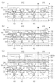
図16は、本発明の第4の実施形態に係る半導体装置(シールリングの周りに、チップ領域を2重に且つ不連続に且つ不連続部分が互いに隣り合わないように配置された複数の空隙を含む空隙領域105a及び105bと、3重の応力吸収壁81a、81b及び81cとを有する半導体装置)が設けられているウェハの一部分を示す平面図である。
FIG. 16 shows a semiconductor device according to a fourth embodiment of the present invention (a plurality of gaps arranged around the seal ring so that the chip regions are doubly and discontinuously and the discontinuous portions are not adjacent to each other. 1 is a plan view showing a part of a wafer provided with a semiconductor device having
空隙領域105a及び105bは、それぞれ不連続に配置された複数の空隙を含むと共に、空隙領域105aと空隙領域105bとにおける空隙の不連続部分が互いに隣り合わないように配置されている。つまり、第4の実施形態に係る半導体装置は、二つの空隙領域105a及び105bがいずれも不連続に配置された空隙を含み且つ空隙の不連続部分が互いに隣り合わないようになっている二重構造の空隙領域となっている点を除いて、第3の実施形態に係る半導体装置と同様の構造を有している。
The
このことを、更に図17及び図18を用いて示す。図17は、図15のXVII-XVII'線における断面図である。つまり、チップ領域102の周縁部に位置するシールリング103を含む半導体装置端部(具体的には、チップ領域102の配線構造及びシールリング103の構造)の断面図である。また、図18は、図15のXVII-XVII'線の近傍を拡大した平面図である。尚、図17には、二重構造の空隙領域105a及び105bをそれぞれ構成する複数の空隙(41a、41b)が互いに隣り合う箇所(例えば、図18におけるA線)を含むような断面を示している。
This is further illustrated with reference to FIGS. 17 is a cross-sectional view taken along line XVII-XVII ′ of FIG. That is, it is a cross-sectional view of the semiconductor device end portion (specifically, the wiring structure of the
また、図16〜図18に示す構造を有する第4の実施形態に係る半導体装置の製造方法は、使用されるフォトマスクにおける空隙形成用マスクパターンのレイアウトを除いて、基本的に、第1の実施形態に係る半導体装置の製造方法と同様である。 Also, the manufacturing method of the semiconductor device according to the fourth embodiment having the structure shown in FIGS. 16 to 18 is basically the same as the first method except for the layout of the void forming mask pattern in the photomask used. This is the same as the semiconductor device manufacturing method according to the embodiment.
以上に説明したように、第4の実施形態に係る半導体装置の製造方法によると、チップ領域102のビア21、23、25及び配線22、24、26を形成すると同時に、シールビア31、33、35及びシール配線32、34、36からなるシールリング103を形成できる。さらに、シールリング103の外側に、3重構造を持つ応力吸収壁(3つの応力吸収壁81a、81b及び81c)と、2重構造を持つ空隙領域(2つの空隙領域105a及び105b)とを形成できる。
As described above, according to the semiconductor device manufacturing method of the fourth embodiment, the
第4の実施形態に係る半導体装置によると、次のような効果がある。つまり、半導体装置が形成されたウェハである基板11は、ダイシング領域101に沿ってダイシングを行なうことによって、個々の半導体装置(半導体チップ)に分離される。
The semiconductor device according to the fourth embodiment has the following effects. That is, the
ダイシング時に発生するクラックや衝撃等がチップ領域102内に侵入すると、シールリング103又は更にその内側の部分に損傷を与える恐れがある。これを防ぐために本実施形態の半導体装置には空隙領域が設けられているが、それぞれの空隙領域105a及び15bはいずれも空隙が不連続に配置された構成を有するため、空隙の不連続部分をクラックや衝撃等が通り抜ける場合が考えられる。しかし、本実施形態の半導体装置において、外側の空隙領域105bに含まれる空隙の不連続部分と、内側の空隙領域105aに含まれる複空隙の不連続部分とは、シールリング103の伸びる方向に対して垂直な方向に関し、互いに隣り合わないようになっている。よって、外側の空隙領域105bにおける不連続部分を通過した(そのため空隙領域105bによって阻止されたなかった)クラックや衝撃は、必ず内側の空隙領域105aの空隙によって阻止される。
If cracks, impacts, or the like generated during dicing enter the
言い換えると、ダイシング領域101側からチップ領域102を見た場合には、多重の空隙領域を構成する複数の空隙が隙間なく配置されていることになるため、ウェハダイシング部分からチップ領域の内部方向へのクラックや衝撃等の進行を確実に防ぐことができる。よって、ダイシング時のクラックや衝撃等がシールリングに到達する前にそれらを阻止することができるので、シールリングが欠損したり又はシールリングが破壊されたりすることはない。このため、チップ領域の内部を確実に保護するというシールリングの機能が損なわれることがない。以上のように、シールリング103がダメージを受けることを防止できるので、シールリング103の本来の機能である、外部からチップ領域102の内部に水分や可動イオン等が浸入することを防ぐ機能を保持することができ、それによって信頼性の高い半導体装置を提供することができる。なお、不連続部分が互いに隣り合わない構造であれば、空隙領域105a及び105bに含まれる空隙(41a及び41b)の長さは任意でも良い。
In other words, when the
シールリングと平行に伸びる連続した空隙を設けると、機械的強度が低下する原因となる。この点から、複数の空隙を不連続に配置する方が望ましい。このようにすると不連続部分をクラックや衝撃が通過することが考えられるが、不連続部分が隣り合わないように空隙を2重以上に配置することにより、内側の不連続部分を通過してクラックや衝撃がシールリングに到達するのを防ぐことができる。 Providing a continuous gap extending parallel to the seal ring causes a decrease in mechanical strength. In this respect, it is desirable to discontinuously arrange a plurality of gaps. In this way, cracks and impacts may pass through the discontinuous part, but by disposing the gaps more than twice so that the discontinuous parts do not adjoin each other, cracks pass through the inner discontinuous part. And impact can be prevented from reaching the seal ring.
また、本実施形態の半導体装置においては空隙41が不連続に形成されているが、これに代えて、応力吸収体を不連続に形成する構成を取ることも可能である。例えば、第1の実施形態において、応力吸収体72をシールリング103の延びる方向に関して不連続に形成した場合について図19に示す。これは、図3を置き換える図と考えればよい。ここで、本実施形態における空隙41a及び空隙41bの配置と同様に、2つの応力吸収壁81a及び81bに含まれるそれぞれの応力吸収体72について、不連続部分が互いに隣り合わないように配置されている。このため、空隙について本実施形態にて説明したのと同様に、ダイシング領域101側からチップ領域102を見た場合には、多重の応力吸収壁を構成する複数の応力吸収体が隙間なく配置されている。結果として、チップ領域102の内部を確実に保護することができる。
In the semiconductor device according to the present embodiment, the
尚、上記第1から第4の実施形態において、シールリング103としてシールビアと、シールビアよりも幅の広いシール配線とによる積層構造を用いた。しかし、シール配線の幅をシールビアの幅と同等にしてもなんら問題はない。また、シールリング103としてシールビアとシール配線の積層構造を用いたが、シールビア工程のみで形成しても何なんら問題はない。これら構造とすることにより、シールビアとシール配線との積層構造を用いる場合と比べて、半導体装置内におけるシールリング103の幅方向(チップ領域102の周縁に沿ってシールリング103が延びる方向に対して垂直な方向)の占有領域を狭くできるので、半導体装置の小型化に有効である。
In the first to fourth embodiments, a laminated structure including a seal via and a seal wiring wider than the seal via is used as the
また、上記第1から第4の実施形態において、最下層の配線(第1のビア21と第1の配線22)を除きデュアルダマシン方式により形成した。しかし、ビア(及びシールビア)又は配線(及びシール配線)の開口部、すなわちビアホール又は配線溝を形成した後、それぞれ独立して金属を埋め込むシングルダマシン法を用いても良い。 In the first to fourth embodiments, the dual damascene method is used except for the lowermost wiring (the first via 21 and the first wiring 22). However, it is also possible to use a single damascene method in which a metal is independently embedded after forming an opening of a via (and a seal via) or a wiring (and a seal wiring), that is, a via hole or a wiring groove.
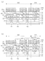
この場合の断面形状の例を図20に示す。ここでは、第4の層間絶縁膜16及び第6の層間絶縁膜18がいずれも2層の積層構造となっており、第4の層間絶縁膜16の下側の層(第2のビア23が形成されている層)にも応力吸収体74が形成されている。このため、図20の半導体装置は、積層された層間絶縁膜の厚さ方向について複数の応力吸収体(71、74及び72)が隣接して形成された構造を有している。
An example of the cross-sectional shape in this case is shown in FIG. Here, each of the fourth
これに対し、応力吸収体形成をビア形成または配線形成のいずれか一方のマスクのみで行ってもよく、応力吸収体はシールリング103と平行に不連続に複数形成された構造となる。
On the other hand, the stress absorber may be formed using only one of the masks for via formation or wiring formation, and a plurality of stress absorbers are formed discontinuously in parallel with the
また、図21に示す通り、空隙を層間絶縁膜の厚さ方向に隣接して形成しても良い。応力吸収体又は空隙を層間絶縁膜の厚さ方向に隣接して形成すると、ダイシングの際の応力やクラック等を確実に防ぐことができる。 Further, as shown in FIG. 21, the gap may be formed adjacent to the thickness direction of the interlayer insulating film. If the stress absorber or void is formed adjacent to the thickness direction of the interlayer insulating film, stress, cracks, and the like during dicing can be reliably prevented.
また、上記第1から第4の実施形態において、応力吸収壁(81a、81b、81c)に含まれる応力吸収体と、空隙領域105(105a及び105b)に含まれる空隙とは、少なくとも1つの層間絶縁膜に形成されていれば良い。また、一般的に機械的強度の低い膜として知られる例えば炭素含有シリコン酸化膜からなる層間膜を用いた層にのみ選択的に形成しても良い。 In the first to fourth embodiments, the stress absorber included in the stress absorption walls (81a, 81b, 81c) and the void included in the void region 105 (105a and 105b) are at least one interlayer. What is necessary is just to be formed in the insulating film. Alternatively, it may be selectively formed only on a layer using an interlayer film made of, for example, a carbon-containing silicon oxide film, which is generally known as a film having low mechanical strength.
また、上記第1から第4の実施形態において、応力吸収体及び空隙は、ダイシング領域101に形成した。しかし、応力吸収体及び空隙領域は、ウェハダイシング部分とシールリング103との間に設けられていれば良いのであり、各実施形態の形成位置に限られるものではない。例えば、応力吸収体及び空隙を、シールリング103の外側であって、チップ領域102内におけるダイシング領域101との境界付近に設けてもよい。
In the first to fourth embodiments, the stress absorber and the gap are formed in the
また、上記第1から第4の実施形態において、シールリング103を、チップ領域102におけるダイシング領域101との境界付近に設けたが、これに代えて、空隙領域105の内側であって、例えばダイシング領域101のうちダイシング後も半導体装置(半導体チップ)の端部として残る部分(つまりダイシング領域101におけるチップ領域102との境界付近)に設けてもよい。
Further, in the first to fourth embodiments, the
また、上記第1から第4の実施形態において、6層重ねられた層間絶縁膜に3層の配線及び3層のビアを形成したが、層間絶縁膜の層数は6層に限られるものではないし、また配線及びビアが3層に限られるものでもなく、チップ構造に応じてより少なくても多くても良い。 In the first to fourth embodiments, three layers of wiring and three layers of vias are formed in the six interlayer insulating films, but the number of interlayer insulating films is not limited to six. In addition, the wiring and vias are not limited to three layers, and may be more or less depending on the chip structure.
また、上記第1から第4の実施形態において、シールリング103として縦方向に一連のシールリング構造を示したが、一連のシールリング構造に限定されるものではない。例えば2連以上の構造を有しても良いし、また、シールリング構造は一部が枝分かれした構造を有してもよい。
In the first to fourth embodiments, a series of seal ring structures are shown in the vertical direction as the
また、上記第1から第4の実施形態において、各配線及び各ビアと、シールリング103とを構成する導電材料としてCuを用いたが、これには限られず、W、Al及びCuのうちの少なくとも1つを用いて構成してもよい。このようにすると、半導体装置のチップ領域102に形成される配線及びビアと同じ材料からシールリング103を形成することができる。
Further, in the first to fourth embodiments, Cu is used as a conductive material constituting each wiring and each via and the
また、上記第1〜第4の実施形態において、第1〜第6の層間絶縁膜およびパッシベーション膜はそれぞれ単一の膜として使用していたが、少なくともいずれか1つの層間絶縁膜又はパッシベーション膜を2種類以上の膜からなる積層構造としてもよい。 In the first to fourth embodiments, the first to sixth interlayer insulating films and the passivation film are each used as a single film. However, at least one of the interlayer insulating films or the passivation film is used. It is good also as a laminated structure which consists of two or more types of films | membranes.
例えば、図22に示すように、第4の層間絶縁膜について、配線が形成される層とビアが形成される層とが互いに異なる比誘電率を有する炭素含有シリコン酸化膜によって形成されている構造としても良い。このとき、2種類の炭素含有シリコン酸化膜について、配線が形成される層間絶縁膜の比誘電率(k1)が、ビアが形成される層間絶縁膜の比誘電率(k2)に比べて低い(k1<k2)様な組み合わせであってもよい。つまり、配線が形成される層間絶縁膜の方が、ビアが形成される層間絶縁膜に比べて炭素濃度が高い又は空孔量が多い(それにより、比誘電率が低い)というような異なる層間絶縁膜の組み合わせとするということである。 For example, as shown in FIG. 22, in the fourth interlayer insulating film, the layer in which the wiring is formed and the layer in which the via is formed are formed of carbon-containing silicon oxide films having different relative dielectric constants. It is also good. At this time, for the two types of carbon-containing silicon oxide films, the relative dielectric constant (k1) of the interlayer insulating film in which the wiring is formed is lower than the relative dielectric constant (k2) of the interlayer insulating film in which the via is formed ( A combination such as k1 <k2) may be used. In other words, the interlayer insulating film in which the wiring is formed has a different carbon interlayer concentration or a larger amount of holes (and thus has a lower relative dielectric constant) than the interlayer insulating film in which the via is formed. That is, a combination of insulating films.
更に、配線層に用いる層間絶縁膜の比誘電率が、ビア層に用いる層間絶縁膜の比誘電率より低くなるような組み合わせとして、ビア層にはTEOS等のシリコン酸化膜又はフッ素含有シリコン酸化膜を用い、配線層にはフッ素含有シリコン酸化膜又は炭素含有シリコン酸化膜等を用いてもよい。 Further, the via layer is formed of a silicon oxide film such as TEOS or a fluorine-containing silicon oxide film in such a combination that the relative dielectric constant of the interlayer insulating film used for the wiring layer is lower than the relative dielectric constant of the interlayer insulating film used for the via layer. The wiring layer may be a fluorine-containing silicon oxide film or a carbon-containing silicon oxide film.
上記のような膜構造とすることにより、配線が形成された層における配線間の容量を低減することが可能となる。比誘電率が低い絶縁膜は一般的に機械強度が低くダイシングによる損傷を受けやすいが、このような機械強度の低い膜を適用した層に対して選択的に本発明の空隙を形成することにより、ダイシング時の応力やクラックの伝播を防止しシールリングを保護することが可能となる。 With the above film structure, it is possible to reduce the capacitance between the wirings in the layer in which the wiring is formed. An insulating film having a low relative dielectric constant generally has low mechanical strength and is easily damaged by dicing. However, by selectively forming the voids of the present invention with respect to a layer to which such a low mechanical strength film is applied. It is possible to prevent the propagation of stress and cracks during dicing and protect the seal ring.
また、第3の層間絶縁膜には一般的にCuの拡散防止機能と、ビアパターン形成時のエッチストップ機能が求められる。そこで、第3の層間絶縁膜を例えば窒素含有の炭化シリコン膜と酸素含有の炭化シリコン膜の積層構造とすると、膜の比誘電率が低いため、上記Cu拡散防止機能とエッチストップ機能とを有しつつ、配線の配線間容量の増大を防止する効果がある。 The third interlayer insulating film is generally required to have a Cu diffusion preventing function and an etch stop function when forming a via pattern. Therefore, if the third interlayer insulating film has a laminated structure of, for example, a nitrogen-containing silicon carbide film and an oxygen-containing silicon carbide film, the film has a low relative dielectric constant, and therefore has the Cu diffusion prevention function and the etch stop function. However, there is an effect of preventing an increase in inter-wiring capacitance of the wiring.
一般的に、SiNはNを含有することによりCu拡散防止能があることが知られており、比誘電率は約7である。SiCの比誘電率は約3.5であるが、Cu拡散防止能が低い。このため、Nを添加してSiCNにすることにより、低誘電率(約4.8)とCu拡散防止の機能を持たせることができる。また、SiCOはSiCNよりも低誘電率(約4.6)であるが、Oを含むためにCuが酸化してしまう。そのため、SiCNがCu側に来るように積層して使用する。以上の説明から分かるように、低誘電率膜等の層間膜に対して、SiCN、SiCOともにエッチストップ機能を有している。 In general, SiN is known to have Cu diffusion preventing ability by containing N, and its relative dielectric constant is about 7. Although the relative dielectric constant of SiC is about 3.5, the Cu diffusion preventing ability is low. For this reason, by adding N to SiCN, it is possible to have a low dielectric constant (about 4.8) and a function of preventing Cu diffusion. SiCO has a lower dielectric constant (about 4.6) than SiCN, but Cu is oxidized because it contains O. Therefore, it is used by stacking so that SiCN comes to the Cu side. As can be understood from the above description, both SiCN and SiCO have an etch stop function with respect to an interlayer film such as a low dielectric constant film.
更に、パッシベーションを2種類以上の膜からなる積層構造とすることの効果として、以下のような効果が考えられる。例えば、第6の層間絶縁膜と同層に形成されている配線の直上にはシリコン窒化膜に比べて比誘電率の低い酸素又は窒素含有の炭化シリコン膜を形成し、更にその表面にシリコン窒化膜を形成する構造とすることにより、配線の配線間容量の増大を防止することができる。 Furthermore, the following effects can be considered as an effect of providing a laminated structure composed of two or more kinds of passivation. For example, an oxygen or nitrogen-containing silicon carbide film having a relative dielectric constant lower than that of the silicon nitride film is formed immediately above the wiring formed in the same layer as the sixth interlayer insulating film, and silicon nitride is further formed on the surface thereof. By adopting a structure in which a film is formed, an increase in inter-wiring capacitance can be prevented.
また、単一のパッシベーション膜が有する膜ストレスを、積層構造とすることにより緩和する効果がある。つまり、膜ストレスにより反りが発生したとしても、積層構造であればそれぞれの膜厚は一層構造膜に比べ薄く、個々のストレス量も低くなる。また、積層構造には、界面が存在するために、歪が緩和される。そこで、パッシベーション膜を積層構造とすることにより、膜ストレスを緩和することができる。 In addition, there is an effect of mitigating the film stress of a single passivation film by using a laminated structure. In other words, even if warping occurs due to film stress, the thickness of each layer is thinner than that of the structure film, and the amount of individual stress is also reduced in the case of a laminated structure. In addition, since an interface exists in the laminated structure, strain is reduced. Therefore, film stress can be alleviated by forming the passivation film in a laminated structure.
尚、上記第1〜第4の実施形態において、配線構造及び他の配線構造における配線同士の間に配線間空隙91を形成している。このような配線間空隙91を設けることにより、配線同士の間の容量を低減させることができ、高速動作が可能となる。また、配線間空隙91を形成する際に、同時に第1の空隙41を形成することができ、製造工程を簡略化できる。但し、半導体装置に要求される特性によっては、配線間空隙91を必ずしも設けなくとも良い。
In the first to fourth embodiments, the
以上に説明したように、本発明は、チップ領域の周囲を取り囲むように形成されたシールリングとそれを保護する機構とを有する半導体装置及びその製造方法に関し、ダイシング時に発生するクラックや応力等をシールリングの外側に形成した空隙領域によって阻止してチップ領域の内部を確実に保護するシールリングの機能を保持するという効果が得られ、非常に有用である。 As described above, the present invention relates to a semiconductor device having a seal ring formed so as to surround the periphery of a chip region and a mechanism for protecting the same, and a method for manufacturing the semiconductor device. The effect of retaining the function of the seal ring that is prevented by the gap region formed outside the seal ring and reliably protects the inside of the chip region is very useful.
11 基板(半導体基板)
12 素子分離膜
13 第1の層間絶縁膜
14 第2の層間絶縁膜
15 第3の層間絶縁膜
16 第4の層間絶縁膜
17 第5の層間絶縁膜
18 第6の層間絶縁膜
19 パッシベーション膜
21 第1のビア
21a 第1のビアホール
22 第1の配線
22a 第1の配線溝
22b 配線溝パターン
23 第2のビア
23a 第2のビアホール
23b 第2のビアホールパターン
24 第2の配線
24a 第2の配線溝
24b 第2の配線溝パターン
25 第3のビア
26 第3の配線
27 パッド
27a パッド開口部
27a パッド溝
27b パッド溝パターン
31 第1のシールビア
31a 第1のシールビアホール
32 第1のシール配線
32a 第1のシール配線溝
32b シール配線溝パターン
33 第2のシールビア
33a 第2のシールビアホール
33b 第2のシールビアパターン
34 第2のシール配線
34a 第2のシール配線溝
34b 第2のシール配線溝パターン
35 第3のシールビア
36 第3のシール配線
37 キャップ
37a キャップ溝
37b キャップ溝形成パターン
41 第1の空隙
41a 第1の空隙形成用溝
41b 第1の空隙形成用パターン
51 レジスト
52 ビアパターン形成用レジスト
53 レジスト
54 パッシベーション膜加工用レジスト
55 レジスト
61 活性層
62 活性層
71 第1の応力吸収体
71a 第1の応力吸収体形成用溝
71b 第1の応力吸収体形成用パターン
72 第2の応力吸収体
72a 第2の応力吸収体形成用溝
72b 第2の応力吸収体形成用パターン
73 第3の応力吸収体
81a、82b、83c 応力吸収壁
91 配線間空隙
91a 配線間空隙形成領域
91b 配線間空隙形成用溝
101 ダイシング領域
102 チップ領域
103 シールリング
105、105a、105b 空隙領域
11 Substrate (semiconductor substrate)
12 element isolation film 13 first interlayer insulating film 14 second interlayer insulating film 15 third interlayer insulating film 16 fourth interlayer insulating film 17 fifth interlayer insulating film 18 sixth interlayer insulating film 19 passivation film 21 First via 21a First via hole 22 First wiring 22a First wiring groove 22b Wiring groove pattern 23 Second via 23a Second via hole 23b Second via hole pattern 24 Second wiring 24a Second wiring Groove 24b Second wiring groove pattern 25 Third via 26 Third wiring 27 Pad 27a Pad opening 27a Pad groove 27b Pad groove pattern 31 First seal via 31a First seal via hole 32 First seal wiring 32a First 1 seal wiring groove 32b seal wiring groove pattern 33 second seal via 33a second seal via hole 33b second seal A pattern 34 Second seal wiring 34a Second seal wiring groove 34b Second seal wiring groove pattern 35 Third seal via 36 Third seal wiring 37 Cap 37a Cap groove 37b Cap groove formation pattern 41 First gap 41a First gap forming groove 41b First gap forming pattern 51 Resist 52 Via pattern forming resist 53 Resist 54 Passivation film processing resist 55 Resist 61 Active layer 62 Active layer 71 First stress absorber 71a First Stress absorber forming groove 71b First stress absorber forming pattern 72 Second stress absorber 72a Second stress absorber forming groove 72b Second stress absorber forming pattern 73 Third stress absorber 81a, 82b, 83c Stress absorbing wall 91 Wiring gap 91a Wiring gap forming area 91b Wiring gap Gap for forming gap 101 Dicing area 102 Chip area 103 Seal ring 105, 105a, 105b Gap area
Claims (28)
前記基板上に形成された絶縁膜と、
前記絶縁膜中に、前記素子の形成された領域を取り囲み且つ前記絶縁膜を貫通するように形成されたシールリングと、
前記素子から見て前記シールリングよりも外側に位置する部分の前記絶縁膜に形成され、少なくとも1つの応力吸収体を含む応力吸収壁と、
前記素子から見て前記シールリングよりも外側に位置する部分の前記絶縁膜に形成され、少なくとも1つの空隙を含む空隙領域とを備えることを特徴とする半導体装置。 An element formed on a substrate;
An insulating film formed on the substrate;
A seal ring formed in the insulating film so as to surround the region where the element is formed and to penetrate the insulating film;
A stress-absorbing wall formed on the insulating film in a portion located outside the seal ring when viewed from the element and including at least one stress absorber;
A semiconductor device comprising: a gap region formed on the insulating film in a portion located outside the seal ring as viewed from the element and including at least one gap.
前記絶縁膜は、複数の層間絶縁膜が積層された構造を有し、
前記複数の層間絶縁膜のうちの少なくとも1つの層間絶縁膜に形成され且つ前記素子に電気的に接続されたビアと、
前記複数の層間絶縁膜のうちの少なくとも1つの層間絶縁膜に形成され且つ前記素子に電気的に接続された配線とを備え、
前記シールリングは、前記ビアが形成された前記層間絶縁膜に形成されたシールビアと、前記配線が形成された前記層間絶縁膜に形成されたシール配線とを含み、
前記応力吸収壁は、少なくとも、前記複数の層間絶縁膜のうちの前記シール配線が形成されている層間絶縁膜に形成された応力吸収体を含み、
前記空隙領域は、少なくとも、前記複数の層間絶縁膜のうちの前記シール配線が形成されている層間絶縁膜に形成された空隙を含むことを特徴とする半導体装置。 In claim 1,
The insulating film has a structure in which a plurality of interlayer insulating films are laminated,
A via formed in at least one of the plurality of interlayer insulating films and electrically connected to the element;
A wiring formed on at least one of the plurality of interlayer insulating films and electrically connected to the element;
The seal ring includes a seal via formed in the interlayer insulating film in which the via is formed, and a seal wiring formed in the interlayer insulating film in which the wiring is formed,
The stress absorbing wall includes at least a stress absorber formed in an interlayer insulating film in which the seal wiring is formed among the plurality of interlayer insulating films,
The gap region includes at least a gap formed in an interlayer insulating film in which the seal wiring is formed among the plurality of interlayer insulating films.
前記配線と前記ビアとは、それぞれ前記複数の層間絶縁膜のうちの異なる層間絶縁膜中に形成されていることを特徴とする半導体装置。 In claim 2,
The wiring device and the via are formed in different interlayer insulating films among the plurality of interlayer insulating films, respectively.
前記複数の層間絶縁膜のうちの前記配線が形成されている層間絶縁膜は、前記複数の層間絶縁膜のうちの前記ビアが形成されている層間絶縁膜よりも誘電率が低い膜からなることを特徴とする半導体装置。 In claim 3,
Of the plurality of interlayer insulating films, the interlayer insulating film in which the wiring is formed is a film having a lower dielectric constant than the interlayer insulating film in the plurality of interlayer insulating films in which the via is formed. A semiconductor device characterized by the above.
前記ビア及び前記配線が一体的に形成されたデュアルダマシン配線を含むことを特徴とする半導体装置。 In claim 2,
A semiconductor device comprising: a dual damascene wiring in which the via and the wiring are integrally formed.
前記絶縁膜の上に形成されたパッシベーション膜を更に備え、
前記シールリングは、前記絶縁膜に加えて前記パッシベーション膜についても貫通するように形成され、
前記空隙領域は、前記素子から見て前記シールリングよりも外側に位置する部分の前記パッシベーション膜中に形成されているスリットを更に含むことを特徴とする半導体装置。 In any one of Claims 1-5,
Further comprising a passivation film formed on the insulating film;
The seal ring is formed so as to penetrate the passivation film in addition to the insulating film,
The semiconductor device according to claim 1, wherein the gap region further includes a slit formed in the passivation film in a portion located outside the seal ring when viewed from the element.
前記パッシベーション膜は、複数の膜からなる積層構造を有することを特徴とする半導体装置。 In claim 6,
The semiconductor device according to claim 1, wherein the passivation film has a laminated structure including a plurality of films.
前記応力吸収壁は、前記絶縁膜の厚さ方向に不連続に配置された複数の応力吸収体を含むことを特徴とする半導体装置。 In any one of Claims 1-7,
The semiconductor device according to claim 1, wherein the stress absorbing wall includes a plurality of stress absorbers arranged discontinuously in a thickness direction of the insulating film.
前記応力吸収壁は、前記絶縁膜の厚さ方向に隣接するように配置された複数の応力吸収体を含むことを特徴とする半導体装置。 In any one of Claims 1-7,
The semiconductor device according to claim 1, wherein the stress absorption wall includes a plurality of stress absorbers arranged adjacent to each other in a thickness direction of the insulating film.
前記応力吸収壁は、前記素子から見て前記シールリングの外側を切れ目無く連続して取り囲むように形成された応力吸収体を含むことを特徴とする半導体装置。 In any one of Claims 1-9,
The semiconductor device according to claim 1, wherein the stress absorbing wall includes a stress absorber formed so as to continuously surround the outside of the seal ring as viewed from the element.
前記応力吸収壁は、前記素子から見て前記シールリングの外側を不連続に取り囲むように配置された複数の応力吸収体を含むことを特徴とする半導体装置。 In any one of Claims 1-9,
The semiconductor device according to claim 1, wherein the stress absorbing wall includes a plurality of stress absorbers disposed so as to discontinuously surround the outside of the seal ring when viewed from the element.
前記素子から見て前記応力吸収壁の外側に、少なくとも1つの応力吸収体を含む少なくとも1つの他の応力吸収壁を更に備えることを特徴とする半導体装置。 In any one of Claims 1-11,
A semiconductor device further comprising at least one other stress absorbing wall including at least one stress absorbing body outside the stress absorbing wall as viewed from the element.
前記他の応力吸収壁は、前記素子から見て前記シールリングの外側を切れ目無く連続して取り囲むように形成された応力吸収体を含むことを特徴とする半導体装置。 In claim 12,
The other stress absorption wall includes a stress absorber formed so as to continuously surround the outside of the seal ring as viewed from the element.
前記他の応力吸収壁は、前記素子から見て前記シールリングの外側を不連続に取り囲むように配置された複数の応力吸収体を含むことを特徴とする半導体装置。 In claim 12,
The other stress absorption wall includes a plurality of stress absorbers disposed so as to discontinuously surround the outside of the seal ring when viewed from the element.
前記応力吸収壁及び前記他の応力吸収壁は、それぞれ、前記素子から見て前記シールリングの外側を不連続に取り囲むように配置された複数の応力吸収体を含み、
前記応力吸収壁における複数の応力吸収体同士の間の部分と、前記他の応力吸収壁における複数の応力吸収体の間の部分とは、前記シールリングの延びる方向に垂直な方向について互いに隣り合わないように配置されていることを特徴とする半導体装置。 In claim 12,
The stress absorbing wall and the other stress absorbing wall each include a plurality of stress absorbers disposed so as to discontinuously surround the outside of the seal ring when viewed from the element,
The portion between the plurality of stress absorbers on the stress absorbing wall and the portion between the plurality of stress absorbers on the other stress absorbing wall are adjacent to each other in the direction perpendicular to the extending direction of the seal ring. A semiconductor device, wherein the semiconductor device is arranged so as not to exist.
前記シールリングを囲むように配置された複数の応力吸収体のうちの少なくとも1つの応力吸収体は、前記シールリングの延びる方向の寸法が他の応力吸収体とは異なるように形成されていることを特徴とする半導体装置。 In claim 11, 14 or 15,
At least one of the plurality of stress absorbers arranged so as to surround the seal ring is formed so that the dimension in the extending direction of the seal ring is different from other stress absorbers. A semiconductor device characterized by the above.
前記空隙領域は、前記絶縁膜の厚さ方向に不連続に配置された複数の空隙を含むことを特徴とする半導体装置。 In any one of Claims 1-16,
The gap region includes a plurality of gaps that are discontinuously arranged in the thickness direction of the insulating film.
前記空隙領域は、前記絶縁膜の厚さ方向に隣接するように配置された複数の空隙を含むことを特徴とする半導体装置。 In any one of Claims 1-16,
The gap region includes a plurality of gaps arranged so as to be adjacent to each other in the thickness direction of the insulating film.
前記空隙領域は、前記素子から見て前記シールリングの外側を切れ目無く連続して取り囲むように形成された空隙を含むことを特徴とする半導体装置。 In any one of Claims 1-18,
The semiconductor device according to claim 1, wherein the void region includes a void formed so as to continuously surround the outside of the seal ring as viewed from the element.
前記空隙領域は、前記素子から見て前記シールリングの外側を不連続に取り囲むように配置された複数の空隙を含むことを特徴とする半導体装置。 In any one of Claims 1-18,
The gap region includes a plurality of gaps arranged so as to discontinuously surround the outside of the seal ring when viewed from the element.
前記素子から見て前記空隙領域の外側に、少なくとも1つの空隙を含む少なくとも1つの他の空隙領域を更に備えることを特徴とする半導体装置。 In any one of Claims 1-20,
A semiconductor device, further comprising at least one other void region including at least one void outside the void region when viewed from the element.
前記他の空隙領域は、前記素子から見て前記シールリングの外側を切れ目無く連続して取り囲むように形成された空隙を含むことを特徴とする半導体装置。 In claim 21,
The other gap region includes a gap formed so as to continuously surround the outside of the seal ring as viewed from the element.
前記他の空隙領域は、前記素子から見て前記シールリングの外側を不連続に取り囲むように配置された複数の空隙を含むことを特徴とする半導体装置。 In claim 21,
The other gap region includes a plurality of gaps disposed so as to discontinuously surround the outside of the seal ring when viewed from the element.
前記空隙領域及び前記他の空隙領域は、それぞれ、前記素子から見て前記シールリングの外側を不連続に取り囲むように配置された複数の空隙を含み、
前記空隙領域における複数の空隙同士の間の部分と、前記他の空隙領域における複数の空隙の間の部分とは、前記シールリングの延びる方向に垂直な方向について互いに隣り合わないように配置されていることを特徴とする半導体装置。 In claim 21,
The gap area and the other gap area each include a plurality of gaps arranged so as to discontinuously surround the outside of the seal ring as viewed from the element,
A portion between the plurality of gaps in the gap region and a portion between the plurality of gaps in the other gap region are arranged so as not to be adjacent to each other in a direction perpendicular to the extending direction of the seal ring. A semiconductor device characterized by comprising:
前記シールリングを囲むように配置された複数の空隙のうちの少なくとも1つの空隙は、前記シールリングの延びる方向の寸法が他の空隙とは異なるように形成されていることを特徴とする半導体装置。 In claim 20, 23 or 24,
At least one of the plurality of voids arranged so as to surround the seal ring is formed so that the dimension in the extending direction of the seal ring is different from that of the other voids. .
前記素子を形成した前記基板上に、層間絶縁膜を形成する工程と、
前記層間絶縁膜に、前記素子に電気的に接続する配線及びビアの少なくとも一方を形成するための第1の凹部と、前記第1の凹部を取り囲み且つシールリングの少なくとも一部を形成するための第2の凹部と、前記素子から見て前記第2の凹部の外側に応力吸収体を形成するための第3の凹部と、前記素子から見て前記第2の凹部の外側に空隙を形成するための第4の凹部とを形成する工程と、
前記第1の凹部と前記第2の凹部と前記第3の凹部とに導電膜を埋め込むことにより、前記配線及び前記ビアの少なくとも一方と前記シールリングの少なくとも一部と前記応力吸収体を形成すると共に、前記第4の凹部を空隙として残す工程とを備えることを特徴とする半導体装置の製造方法。 Forming an element on a substrate;
Forming an interlayer insulating film on the substrate on which the element is formed;
A first recess for forming at least one of a wiring and a via electrically connected to the element in the interlayer insulating film, and forming at least a part of a seal ring surrounding the first recess A second recess, a third recess for forming a stress absorber outside the second recess viewed from the element, and a gap formed outside the second recess viewed from the element Forming a fourth recess for
By embedding a conductive film in the first recess, the second recess, and the third recess, at least one of the wiring and the via, at least a part of the seal ring, and the stress absorber are formed. And a step of leaving the fourth concave portion as a gap.
前記第1の凹部に、前記ビア及び前記配線を、デュアルダマシン法によって一体的に形成することを特徴とする半導体装置の製造方法。 In claim 26,
A method of manufacturing a semiconductor device, wherein the via and the wiring are integrally formed in the first recess by a dual damascene method.
前記素子を形成した前記基板上に、層間絶縁膜を形成する工程と、
前記層間絶縁膜に、前記素子に電気的に接続する配線及びビアの少なくとも一方を形成するための第1の凹部と、前記第1の凹部を取り囲み且つシールリングの少なくとも一部を形成するための第2の凹部と、前記素子から見て前記第2の凹部の外側に応力吸収体を形成するための少なくとも2つの第3の凹部とを形成する工程と、
前記第1の凹部と前記第2の凹部と前記第3の凹部とに導電膜を埋め込むことにより、前記配線及び前記ビアの少なくとも一方と前記シールリングの少なくとも一部と前記応力吸収体を形成する工程と、
前記応力吸収体に挟まれた部分において前記層間絶縁膜を除去することにより空隙を形成する工程とを備え、
前記少なくとも2つの第3の凹部は、前記素子から見て外側に向かう方向に並んでいることを特徴とする半導体装置の製造方法。 Forming an element on a substrate;
Forming an interlayer insulating film on the substrate on which the element is formed;
A first recess for forming at least one of a wiring and a via electrically connected to the element in the interlayer insulating film, and forming at least a part of a seal ring surrounding the first recess Forming a second recess and at least two third recesses for forming a stress absorber on the outside of the second recess when viewed from the element;
By embedding a conductive film in the first recess, the second recess, and the third recess, at least one of the wiring and the via, at least a part of the seal ring, and the stress absorber are formed. Process,
Forming a void by removing the interlayer insulating film in a portion sandwiched between the stress absorbers,
The method of manufacturing a semiconductor device, wherein the at least two third recesses are arranged in a direction outward from the element.
Priority Applications (1)
| Application Number | Priority Date | Filing Date | Title |
|---|---|---|---|
| JP2007292894A JP2009123733A (en) | 2007-11-12 | 2007-11-12 | Semiconductor device and manufacturing method thereof |
Applications Claiming Priority (1)
| Application Number | Priority Date | Filing Date | Title |
|---|---|---|---|
| JP2007292894A JP2009123733A (en) | 2007-11-12 | 2007-11-12 | Semiconductor device and manufacturing method thereof |
Publications (1)
| Publication Number | Publication Date |
|---|---|
| JP2009123733A true JP2009123733A (en) | 2009-06-04 |
Family
ID=40815612
Family Applications (1)
| Application Number | Title | Priority Date | Filing Date |
|---|---|---|---|
| JP2007292894A Pending JP2009123733A (en) | 2007-11-12 | 2007-11-12 | Semiconductor device and manufacturing method thereof |
Country Status (1)
| Country | Link |
|---|---|
| JP (1) | JP2009123733A (en) |
Cited By (8)
| Publication number | Priority date | Publication date | Assignee | Title |
|---|---|---|---|---|
| JP2009123734A (en) * | 2007-11-12 | 2009-06-04 | Renesas Technology Corp | Semiconductor device and manufacturing method thereof |
| JP2011187898A (en) * | 2010-03-11 | 2011-09-22 | Fujitsu Ltd | Semiconductor device and method of manufacturing the same |
| JP2014165403A (en) * | 2013-02-26 | 2014-09-08 | Renesas Electronics Corp | Semiconductor device and semiconductor wafer |
| KR101770455B1 (en) * | 2014-09-25 | 2017-08-22 | 타이완 세미콘덕터 매뉴팩쳐링 컴퍼니 리미티드 | A semiconductor device and a method for forming the same |
| US9922940B2 (en) | 2016-02-22 | 2018-03-20 | Toshiba Memory Corporation | Semiconductor device including air gaps between interconnects and method of manufacturing the same |
| US10026715B2 (en) | 2015-03-17 | 2018-07-17 | Toshiba Memory Corporation | Semiconductor device and manufacturing method thereof |
| CN113629015A (en) * | 2020-05-08 | 2021-11-09 | 联华电子股份有限公司 | Packaging ring structure |
| US12543561B2 (en) | 2023-03-06 | 2026-02-03 | Nanya Technology Corporation | Circuit structure including at least one air gap and method for manufacturing the same |
-
2007
- 2007-11-12 JP JP2007292894A patent/JP2009123733A/en active Pending
Cited By (10)
| Publication number | Priority date | Publication date | Assignee | Title |
|---|---|---|---|---|
| JP2009123734A (en) * | 2007-11-12 | 2009-06-04 | Renesas Technology Corp | Semiconductor device and manufacturing method thereof |
| JP2011187898A (en) * | 2010-03-11 | 2011-09-22 | Fujitsu Ltd | Semiconductor device and method of manufacturing the same |
| JP2014165403A (en) * | 2013-02-26 | 2014-09-08 | Renesas Electronics Corp | Semiconductor device and semiconductor wafer |
| KR101770455B1 (en) * | 2014-09-25 | 2017-08-22 | 타이완 세미콘덕터 매뉴팩쳐링 컴퍼니 리미티드 | A semiconductor device and a method for forming the same |
| US9991200B2 (en) | 2014-09-25 | 2018-06-05 | Taiwan Semiconductor Manufacturing Company, Ltd. | Air gap structure and method |
| US10354949B2 (en) | 2014-09-25 | 2019-07-16 | Taiwan Semiconductor Manufacturing Company, Ltd. | Air gap structure and method |
| US10026715B2 (en) | 2015-03-17 | 2018-07-17 | Toshiba Memory Corporation | Semiconductor device and manufacturing method thereof |
| US9922940B2 (en) | 2016-02-22 | 2018-03-20 | Toshiba Memory Corporation | Semiconductor device including air gaps between interconnects and method of manufacturing the same |
| CN113629015A (en) * | 2020-05-08 | 2021-11-09 | 联华电子股份有限公司 | Packaging ring structure |
| US12543561B2 (en) | 2023-03-06 | 2026-02-03 | Nanya Technology Corporation | Circuit structure including at least one air gap and method for manufacturing the same |
Similar Documents
| Publication | Publication Date | Title |
|---|---|---|
| JP5235378B2 (en) | Semiconductor device | |
| JP4636839B2 (en) | Electronic devices | |
| JP5448304B2 (en) | Semiconductor device | |
| US7453128B2 (en) | Semiconductor device and method for fabricating the same | |
| KR101581431B1 (en) | Semiconductor chips having guard rings and methods of manufacturing the same | |
| JP5175066B2 (en) | Semiconductor device | |
| US20130285057A1 (en) | Semiconductor device | |
| JP2009123733A (en) | Semiconductor device and manufacturing method thereof | |
| JP2009049313A (en) | Semiconductor device and manufacturing method thereof | |
| JP2008066716A (en) | Semiconductor device | |
| KR20230031712A (en) | Semiconductor device with crack-preventing structure | |
| JP2007019128A (en) | Semiconductor device | |
| CN116487352A (en) | Semiconductor chip including chip protection | |
| JP5483772B2 (en) | Semiconductor device | |
| JP5726989B2 (en) | Semiconductor device | |
| JP5504311B2 (en) | Semiconductor device and manufacturing method thereof |