JP2009106038A - Switching power supply unit - Google Patents
Switching power supply unit Download PDFInfo
- Publication number
- JP2009106038A JP2009106038A JP2007274280A JP2007274280A JP2009106038A JP 2009106038 A JP2009106038 A JP 2009106038A JP 2007274280 A JP2007274280 A JP 2007274280A JP 2007274280 A JP2007274280 A JP 2007274280A JP 2009106038 A JP2009106038 A JP 2009106038A
- Authority
- JP
- Japan
- Prior art keywords
- control
- correction
- current detection
- circuit
- voltage
- Prior art date
- Legal status (The legal status is an assumption and is not a legal conclusion. Google has not performed a legal analysis and makes no representation as to the accuracy of the status listed.)
- Granted
Links
- 238000001514 detection method Methods 0.000 claims description 186
- 238000004804 winding Methods 0.000 claims description 37
- 238000006243 chemical reaction Methods 0.000 claims description 36
- 238000009499 grossing Methods 0.000 claims description 21
- 230000007274 generation of a signal involved in cell-cell signaling Effects 0.000 claims description 13
- 230000007423 decrease Effects 0.000 claims description 7
- 230000004044 response Effects 0.000 claims description 7
- 239000003990 capacitor Substances 0.000 description 15
- 230000008859 change Effects 0.000 description 14
- 238000010586 diagram Methods 0.000 description 13
- 230000006870 function Effects 0.000 description 8
- 230000000694 effects Effects 0.000 description 6
- 230000010355 oscillation Effects 0.000 description 5
- 230000009467 reduction Effects 0.000 description 3
- 230000001360 synchronised effect Effects 0.000 description 3
- 238000013459 approach Methods 0.000 description 2
- 230000005540 biological transmission Effects 0.000 description 2
- 239000004020 conductor Substances 0.000 description 2
- 238000000034 method Methods 0.000 description 2
- 230000015572 biosynthetic process Effects 0.000 description 1
- 230000003247 decreasing effect Effects 0.000 description 1
- 230000001419 dependent effect Effects 0.000 description 1
- 230000005669 field effect Effects 0.000 description 1
- 230000006872 improvement Effects 0.000 description 1
- 238000009413 insulation Methods 0.000 description 1
- 238000012986 modification Methods 0.000 description 1
- 230000004048 modification Effects 0.000 description 1
- 230000003287 optical effect Effects 0.000 description 1
- 229920006395 saturated elastomer Polymers 0.000 description 1
- 239000004065 semiconductor Substances 0.000 description 1
- 230000009131 signaling function Effects 0.000 description 1
- 239000007858 starting material Substances 0.000 description 1
- 230000001960 triggered effect Effects 0.000 description 1
Images


Classifications
-
- H—ELECTRICITY
- H02—GENERATION; CONVERSION OR DISTRIBUTION OF ELECTRIC POWER
- H02M—APPARATUS FOR CONVERSION BETWEEN AC AND AC, BETWEEN AC AND DC, OR BETWEEN DC AND DC, AND FOR USE WITH MAINS OR SIMILAR POWER SUPPLY SYSTEMS; CONVERSION OF DC OR AC INPUT POWER INTO SURGE OUTPUT POWER; CONTROL OR REGULATION THEREOF
- H02M3/00—Conversion of dc power input into dc power output
- H02M3/22—Conversion of dc power input into dc power output with intermediate conversion into ac
- H02M3/24—Conversion of dc power input into dc power output with intermediate conversion into ac by static converters
- H02M3/28—Conversion of dc power input into dc power output with intermediate conversion into ac by static converters using discharge tubes with control electrode or semiconductor devices with control electrode to produce the intermediate ac
- H02M3/325—Conversion of dc power input into dc power output with intermediate conversion into ac by static converters using discharge tubes with control electrode or semiconductor devices with control electrode to produce the intermediate ac using devices of a triode or a transistor type requiring continuous application of a control signal
- H02M3/335—Conversion of dc power input into dc power output with intermediate conversion into ac by static converters using discharge tubes with control electrode or semiconductor devices with control electrode to produce the intermediate ac using devices of a triode or a transistor type requiring continuous application of a control signal using semiconductor devices only
- H02M3/33507—Conversion of dc power input into dc power output with intermediate conversion into ac by static converters using discharge tubes with control electrode or semiconductor devices with control electrode to produce the intermediate ac using devices of a triode or a transistor type requiring continuous application of a control signal using semiconductor devices only with automatic control of the output voltage or current, e.g. flyback converters
- H02M3/33523—Conversion of dc power input into dc power output with intermediate conversion into ac by static converters using discharge tubes with control electrode or semiconductor devices with control electrode to produce the intermediate ac using devices of a triode or a transistor type requiring continuous application of a control signal using semiconductor devices only with automatic control of the output voltage or current, e.g. flyback converters with galvanic isolation between input and output of both the power stage and the feedback loop
-
- H—ELECTRICITY
- H02—GENERATION; CONVERSION OR DISTRIBUTION OF ELECTRIC POWER
- H02M—APPARATUS FOR CONVERSION BETWEEN AC AND AC, BETWEEN AC AND DC, OR BETWEEN DC AND DC, AND FOR USE WITH MAINS OR SIMILAR POWER SUPPLY SYSTEMS; CONVERSION OF DC OR AC INPUT POWER INTO SURGE OUTPUT POWER; CONTROL OR REGULATION THEREOF
- H02M1/00—Details of apparatus for conversion
- H02M1/32—Means for protecting converters other than automatic disconnection
Landscapes
- Engineering & Computer Science (AREA)
- Power Engineering (AREA)
- Dc-Dc Converters (AREA)
Abstract
Description
本発明は、出力電圧を帰還制御によって一定に制御する形式のDC−DCコンバータ等のスイッチング電源装置に関し、更に詳しくは、過電流保護回路を有するスイッチング電源装置に関する。 The present invention relates to a switching power supply device such as a DC-DC converter in which an output voltage is controlled to be constant by feedback control, and more particularly to a switching power supply device having an overcurrent protection circuit.
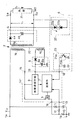
従来の過電流保護回路を有するフライバックタイプのスイッチング電源装置は、図1に示すように、整流平滑回路や蓄電池等の直流電源(図示せず)に接続される第1及び第2の直流電源端子1a、1b、トランス2、Nチャネルの絶縁ゲート型(MOS)電界効果トランジスタで示されているスイッチング素子3、出力整流平滑回路4、第1及び第2の出力端子5a、5b、出力電圧検出回路6、制御部7´、制御電源用整流平滑回路8、制御電源回路9、電流検出抵抗10、第1及び第2の入力電圧補正用抵抗11,12及び入力電圧補正用コンデンサ13を備えている。スイッチング素子3と制御部7´と制御電源回路9とは点線で囲って示す1つの集積回路14´に含まれている。この集積回路14´は第1、第2、第3、第4及び第5の端子15,16,17,18,19を有している。次に、図1の各部を詳しく説明する。
As shown in FIG. 1, a conventional flyback type switching power supply device having an overcurrent protection circuit includes first and second DC power supplies connected to a DC power supply (not shown) such as a rectifying and smoothing circuit or a storage battery.
トランス2は、磁気コア20と、1次巻線N1と、2次巻線N2と、3次巻線(制御電源巻線)N3とから成る。磁気コア20に巻き回され且つ相互に電磁結合された1次、2次及び3次巻線N1,N2,N3は黒丸で示すような極性を有する。従って、スイッチング素子3のオン期間にトランス2にエネルギーが蓄積され、オフ期間にエネルギーが放出される。
The
FETから成るスイッチング素子3は、ドレイン、ソース及び制御電極としてのゲートを有する。このドレインは1次巻線N1を介して第1の直流電源端子1aに接続され、ソースは電流検出抵抗10を介してグランド側の第2の直流電源端子1bに接続され、ゲートは制御部7´に接続されている。
The switching element 3 made of an FET has a drain, a source, and a gate as a control electrode. The drain is connected to the first DC
出力整流平滑回路4は整流ダイオード4aと平滑用コンデンサ4bとから成り、平滑用コンデンサ4bは整流ダイオード4aを介して2次巻線N2に並列に接続されている。整流ダイオード4aはスイッチング素子3のオフ期間に導通する方向性を有する。平滑用コンデンサ4bに接続された第1及び第2の出力端子5a、5bは負荷21を接続するためのものである。
トランス2の3次巻線N3に接続された制御電源用整流平滑回路8は、整流ダイオード8aと平滑コンデンサ8bとから成り、スイッチング素子3がオン・オフ動作を開始した後に制御電源回路9を介して制御部7´に制御用の直流電圧を供給する。
制御電源回路9は集積回路14´の第5の端子19を介して制御電源用整流平滑回路8に接続されていると共に第1の端子15と1次巻線N1とを介して第1の直流電源端子1aに接続され且つ制御部7´の電源端子にも接続されている。この制御電源回路9は、3次巻線N3に電圧が得られる前に第1の直流電源端子1aの電圧で制御部7´を駆動するための周知の起動回路を含む。3次巻線N3に電圧が得られた後に制御部7´は制御電源用整流平滑回路8の電圧で駆動される。
The output rectifying / smoothing circuit 4 includes a rectifying
The control power supply rectifying /
The control
出力電圧検出回路6は、出力電圧を帰還制御するための出力電圧検出手段であって、2次側部分22と1次側部分23とを有する。出力電圧検出回路6の2次側部分22は、第1及び第2の出力端子5a、5b間に接続された発光ダイオード22aと定電圧ダイオード(ツェナーダイオード)22bとの直列回路から成る。発光ダイオード22aは第1及び第2の出力端子5a、5b間の出力電圧Voと定電圧ダイオード22bの基準電圧との差の電圧で駆動され、出力電圧Voに比例した光出力を発生する。出力電圧検出回路6の1次側部分23は、発光ダイオード22aに光結合されたホトトランジスタ23aとコンデンサ23bとから成り、発光ダイオード22aの光出力に反比例したインピーダンス値になる。即ち、ホトトランジスタ23aのインピーダンス値(抵抗値)は出力電圧Voに反比例的に変化する。
The output voltage detection circuit 6 is output voltage detection means for feedback control of the output voltage, and has a
制御部7´は、図2に例示するように大別してPWM信号形成回路と呼ぶこともできるオン・オフ制御信号形成回路24と過電流保護回路25´とローパスフィルタ(LPF)26とを有する。オン・オフ制御信号形成回路24は、出力電圧検出回路6に含めることもできる抵抗27を有する。この抵抗27の一端は制御用直流電圧を供給する直流電源端子27aに接続され、この他端は集積回路14´の第4の端子18を介して図1のホトトランジスタ23aのコレクタに接続されている。従って、直流電源端子27aの電圧が抵抗27とホトトランジスタ23aとで分割される。抵抗27とホトトランジスタ23aとの相互接続点P1とグランドとの間の電圧V1は、ホトトランジスタ23aの両端子間電圧になる。前記電圧V1は出力電圧Voに対して反比例的に変化する。相互接続点P1はフィードバック比較器(コンパレータ)28の負入力端子に接続され、フィードバック比較器28の正入力端子にローパスフィルタ(LPF)26の出力ライン26aが接続されている。ローパスフィルタ(LPF)26は高周波数のノイズを除去するものであり、図1の集積回路14´の第3の端子17と第2の入力電圧補正用抵抗12とを介して電流検出抵抗10の一端に接続されている。従って、フィードバック比較器28の正入力端子に、電流検出抵抗10から得られた電流検出信号を補正したものに相当する補正電流検出信号が入力する。フィードバック比較器28は補正電流検出信号とホトトランジスタ23aから得られた電圧V1とを比較してスイッチング素子3のオン期間の修了時点を示すトリガ信号を出力する。
As illustrated in FIG. 2, the control unit 7 ′ includes an on / off control
フィードバック比較器28の正入力端子の補正電流検出信号の振幅が負入力端子の電圧V1に達すると、フィードバック比較器28の出力端子は高レベル(論理の1)のパルスが発生し、フィードバック比較器28の出力端子に接続されたOR回路(論理和回路)29からも高レベル(論理の1)のパルスが出力される。OR回路29の出力端子はRSフリップフロップ30のリセット端子Rに接続されているので、OR回路(論理和回路)29が高レベル(論理の1)のパルスを出力した時に、RSフリップフロップ30がリセットされる。RSフリップフロップ30のセット端子Sはクロック発生器31に接続されている。クロック発生器31は例えば20〜100kHzでクロック信号を発生する。クロック信号のパルス幅はスイッチング素子3の最低オン時間幅よりも狭い。クロック発生器31からクロック信号が発生すると、これによってRSフリップフロップ30がトリガされてセット状態になる。RSフリップフロップ30のQ-で示す反転出力端子はセット状態の時に低レベル状態(論理の0)になる。NOR回路32の一方の入力端子はRSフリップフロップ30の反転出力端子に接続され、NOR回路32の他方の入力端子はクロック発生器31に接続されている。従って、クロック信号が発生していないと同時にRSフリップフロップ30がセットされている時に、NOR回路32の出力端子に高レベルのパルス(PWMパルス)から成るゲート制御信号(オン・オフ制御信号)が得られ、これが駆動回路33とライン34を介して図1のスイッチング素子3のゲート(制御電極)に供給される。スイッチング素子3はNOR回路32から得られるゲート制御信号が高レベルの時にオン状態になる。
When the amplitude of the correction current detection signal at the positive input terminal of the
次に、電流検出信号及び補正電流検出信号を詳しく説明する。電流検出抵抗10はスイッチング素子3に直列に接続されているので、スイッチング素子3に流れる電流を検出する電流検出手段として機能し、電流検出抵抗10の両端子間にスイッチング素子3に流れる電流に比例した電圧が得られ、これが電流検出信号となる。図1では、第1及び第2の直流電源端子1a、1bの入力電圧Vinの変動による出力電流Ioの最大値即ち最大出力電流の変動を抑制するために、第1の直流電源端子1aと第2の直流電源端子1bとの間に第1の補正用抵抗11を介して補正用コンデンサ13が接続され、電流検出抵抗10が第2の補正用抵抗12を介して補正用コンデンサ13に並列に接続されている。これにより、入力電圧Vinが高くなる程電流検出抵抗10の電圧よりも高い電圧が第3の端子17に得られる。即ち、電流検出抵抗10から得られた電流検出信号を補正した補正電流検出信号が第3の端子17に得られる。周知のようにトランス2の1次巻線N1はインダクタンスを有するので、スイッチング素子3のオン期間にスイッチング素子3を流れる電流は傾斜を有して徐々に増大する。従って、第3の端子17に得られる補正電流検出信号の振幅もスイッチング素子3のオン期間に傾斜を有して徐々に増大する。
もし、図1の第1及び第2の補正用抵抗11,12及び補正用コンデンサ13が設けられていない場合には、オン・オフ制御信号形成回路24及び過電流保護回路25´における遅延の影響によって、図3の実線で示すように入力電圧Vinの上昇に応じて負荷21に供給される出力電流Ioの最大値即ち供給可能な出力電流Ioの最大値(以下、最大出力電流と呼ぶ。)が上昇する。スイッチング電源装置においては、図3の点線で示すように入力電圧Vinの変化に無関係に最大出力電流が一定であることが理想である。図1に示すように補正電流検出信号を形成すると、入力電圧Vinと最大出力電流との関係を図3の点線に近づけることが可能になる。
Next, the current detection signal and the correction current detection signal will be described in detail. Since the
If the first and
制御部7´に含まれている過電流保護回路25´は、過電流検出比較器(コンパレータ)35と、この負入力端子に接続された過電流しきい値付与手段としての過電流基準電圧源36とから成る。過電流検出比較器35の正入力端子はローパスフィルタ(LPF)26の出力ライン26aに接続され、過電流検出比較器35の出力端子はOR回路29に接続されている。ローパスフィルタ(LPF)26の出力ライン26aの補正電流検出信号が過電流基準電圧源36の過電流しきい値としての過電流基準電圧Vrを横切ると、過電流検出比較器35の出力端子からトリガ信号が発生し、このトリガ信号がOR回路29を介してRSフリップフロップ30のリセット端子Rに供給され、RSフリップフロップ30はリセット状態に転換し、スイッチング素子3がオフに転換する。過電流基準電圧Vrは、負荷21が正常状態の時に補正電流検出信号が横切らないように設定され、負荷21が短絡状態又は低インピーダンス状態の時に補正電流検出信号が横切るように設定されている。
The
図1に示すように第1及び第2の補正用抵抗11,12及び補正用コンデンサ13を設けて補正電流検出信号を形成すると、入力電圧Vinと最大出力電流との関係を図3の点線に近づけることが可能になる。しかし、第1及び第2の補正用抵抗11,12及び補正用コンデンサ13が集積回路14´の外付け部品として設けられているので、部品点数の増大によるコストの増大、スイッチング電源装置の寸法の増大を招く。また、第1の補正用抵抗11が第1及び第2の直流電源端子1a,1b間に接続されているので、ここで電力損失が生じ、特に入力電圧Vinが高い時にこの電力損失が大きくなり、スイッチング電源装置の効率低下を招く。この効率低下は、特に入力電圧Vinが高く且つ軽負荷の時に特に大きい。
When the correction current detection signal is formed by providing the first and
入力電圧Vinと最大出力電流との関係を図3の点線に近づける別な方法が、特開2005−184882号公報(特許文献1)に記載されている。この特許文献1の方法では、傾斜電圧発生回路(ランプ波形発生部)と矩形波発生回路とを設け、矩形波電圧に傾斜電圧を重畳している。傾斜電圧発生回路(ランプ波形発生部)はスイッチング素子のオン期間に同期して傾斜電圧を発生するように構成されている。矩形波発生回路は、スイッチング素子のオン期間に同期して矩形波を発生すると同時に入力電圧Vinを検出し、入力電圧Vinに反比例的に矩形波の振幅を変えるように構成されている。これにより、図1のスイッチング電源装置と同様に入力電圧の変化に拘わらず最大出力電流の変化が小さくなる。しかし、矩形波発生回路を設けると、回路装置のスペースの増大を招くのみでなく、矩形波発生回路においても入力電圧Vinを直接検出する方式のために、入力電圧Vinの2乗に比例した電力損失が生じ、スイッチング電源装置の効率の低下を招く。
Another method for bringing the relationship between the input voltage Vin and the maximum output current closer to the dotted line in FIG. 3 is described in Japanese Patent Laid-Open No. 2005-184882 (Patent Document 1). In the method of
スイッチング電源装置は、入力電圧の変化によって最大出力電流が変化するという問題の他に、サブハーモニック現象の問題がある。サブハーモニック現象は、周知のように電流検出信号が外乱などで微小変動すると、スイッチング素子のオン・オフ動作毎にPWM制御信号のオン期間が変動し、収束せずに発振状態又は不安定状態になる現象である。このサブハーモニック現象はPWM制御信号のデューティー比が50%を超えた時に顕著に生じる。このサブハーモニック現象の問題は、特許文献1又は特開2004−40856号公報(特許文献2)に記載されているように電流検出信号に傾斜電圧(スロープ補正信号)を重畳することで解決できる。
本発明が解決しょうとする第1の課題は、入力電圧の変動による最大出力電流の変動を抑制することができるスイッチング電源装置の高効率化及び小型化が要求されていることである。第2の課題は、入力電圧の変化による最大出力電流の変動を抑制することができ且つサブハーモニック現象を抑制することができるスイッチング電源装置の高効率化と小型化が要求されていることである。 The first problem to be solved by the present invention is that there is a demand for high efficiency and miniaturization of a switching power supply capable of suppressing the fluctuation of the maximum output current due to the fluctuation of the input voltage. The second problem is that there is a demand for high efficiency and miniaturization of a switching power supply that can suppress the fluctuation of the maximum output current due to the change of the input voltage and can suppress the subharmonic phenomenon. .
上記第1の課題を解決するための請求項1に従う発明は、
直流電圧を供給するための第1及び第2の直流電源端子と、
1次巻線と該1次巻線に電磁結合された2次巻線とを有するトランスと、
前記トランスの前記1次巻線を介して前記第1及び第2の直流電源端子間に接続され且つオン・オフするための制御電極を有しているスイッチング素子と、
前記トランスの前記2次巻線側の出力電圧を検出する出力電圧検出手段と、
前記出力電圧検出手段と前記スイッチング素子の前記制御電極との間に接続され且つ前記出力電圧を一定に制御するためのオン・オフ制御信号を形成して前記スイッチング素子の前記制御電極に供給する機能を有しているオン・オフ制御信号形成回路と、
前記スイッチング素子を流れる電流を検出するものであって、該電流に対応する電圧値を有している電流検出信号を出力する電流検出手段と、
前記電流検出手段と前記オン・オフ制御信号形成回路とに接続され、前記オン・オフ制御信号形成回路における前記スイッチング素子のオン開始時点を示す信号に応答して前記スイッチング素子のオン時間の経過と共に増大する補正信号(補正電圧)を形成し且つ前記電流検出信号から前記補正信号(補正電圧)を減算して補正電流検出信号を生成する補正電流検出信号生成手段と、
前記スイッチング素子を流れる電流の過電流レベルを示す過電流しきい値(過電流基準電圧)を付与する過電流しきい値付与手段と、
前記補正電流検出信号生成手段に接続され第1の入力端子と前記過電流しきい値付与手段に接続された第2の入力端子と前記オン・オフ制御信号形成回路に接続された出力端子とを有し、前記補正電流検出信号と前記過電流しきい値とを比較して前記補正電流検出信号が前記過電流しきい値に達した時に前記スイッチング素子をオフに制御する出力を前記オン・オフ制御信号形成回路に送る比較手段と
を備えていることを特徴とするスイッチング電源装置に係わるものである。
上記第2の課題を解決するための請求項7に従う発明は、請求項1の補正電流検出信号生成手段の代わりに、前記電流検出手段と前記オン・オフ制御信号形成回路とに接続され、前記スイッチング素子のオン開始時点から所定時間が経過する迄の第1の期間において時間の経過と共に増大する第1の補正信号(補正電圧)を形成し、前記第1の期間の終了時点から前記スイッチング素子のオン期間の終了時点迄の第2の期間において前記第1の期間の終了時点における前記第1の補正信号(補正電圧)の値から時間の経過と共に減少する第2の補正信号(補正電圧)を形成し、且つ前記電流検出信号から前記第1の補正信号及び前記第2の補正信号を順次に減算して補正電流検出信号を生成する補正電流検出信号生成手段備えたスイッチング電源装置に係わるものである。
The invention according to
First and second DC power supply terminals for supplying a DC voltage;
A transformer having a primary winding and a secondary winding electromagnetically coupled to the primary winding;
A switching element connected between the first and second DC power supply terminals via the primary winding of the transformer and having a control electrode for turning on and off;
Output voltage detection means for detecting an output voltage on the secondary winding side of the transformer;
A function connected between the output voltage detecting means and the control electrode of the switching element and forming an on / off control signal for controlling the output voltage to be supplied to the control electrode of the switching element An on / off control signal forming circuit having:
Current detection means for detecting a current flowing through the switching element, and outputting a current detection signal having a voltage value corresponding to the current;
Connected to the current detection means and the on / off control signal forming circuit, and in response to a signal indicating an on start time of the switching element in the on / off control signal forming circuit, with the passage of the on-time of the switching element A correction current detection signal generating means for forming a correction signal (correction voltage) that increases and subtracting the correction signal (correction voltage) from the current detection signal to generate a correction current detection signal;
Overcurrent threshold value applying means for applying an overcurrent threshold value (overcurrent reference voltage) indicating an overcurrent level of the current flowing through the switching element;
A first input terminal connected to the correction current detection signal generating means; a second input terminal connected to the overcurrent threshold value applying means; and an output terminal connected to the on / off control signal forming circuit. And comparing the correction current detection signal with the overcurrent threshold, and when the correction current detection signal reaches the overcurrent threshold, an output for controlling the switching element to be turned off is turned on / off. Comparing means for sending to a control signal forming circuit is provided.
The invention according to claim 7 for solving the second problem is connected to the current detection means and the on / off control signal forming circuit instead of the correction current detection signal generation means of
なお、請求項2及び8に示すように、請求項1及び7の発明のトランスから2次巻線N2を省いた昇圧タイプのスイッチング電源装置に本発明を適用することができる。
また、請求項4に示すように、前記補正信号が所定値よりも高くなることを制限する手段を設けることが望ましい。
また、請求項5に示すように、前記補正回路は、直流電源端子と、グランド端子と、電圧変換用抵抗と、電流変換用抵抗と、第1、第2、第3、第4及び第5の制御素子とを有し、前記電圧変換用抵抗は前記電流検出手段に接続された一端と前記比較手段の前記第1の入力端子に接続された他端とを有し、前記第1、第2、第3、第4及び第5の制御素子のそれぞれは、ソース又はエミッタから成る第1の主電極とドレイン又はコレクタから成る第2の主電極とゲート又はベースから成る制御電極とを有し、前記第1及び第2の制御素子はpチャネル型又はpnp型を有し、前記第3、第4及び第5の制御素子はnチャネル型又はnpn型を有し、前記第1及び第2の制御素子の前記第1の主電極は前記直流電源端子にそれぞれ接続され、前記第1及び第2の制御素子の前記制御電極は互いに接続され且つ前記第1の制御素子の前記第2の主電極に接続され、前記第1の制御素子の前記第2の主電極は前記第3の制御素子の前記第2の主電極に接続され、前記第3の制御素子の前記第1の主電極は前記電流変換用抵抗を介して前記グランド端子に接続され、前記第3の制御素子の前記制御電極は前記傾斜電圧発生回路に接続され、
前記第2の制御素子の前記第2の主電極は前記第4の制御素子の前記第2の主電極に接続され、前記第4の制御素子の前記第1の主電極は直接に又は抵抗を介して前記グランド端子に接続され、前記第4及び第5の制御素子の前記制御電極は互いに接続され且つ前記第4の制御素子の前記第2の主電極に接続され、前記第5の制御素子の前記第1の主電極は直接に又は抵抗を介して前記グランド端子に接続され、前記第5の制御素子の前記第2の主電極は前記電圧変換用抵抗の前記他端に接続されていることが望ましい。
また、請求項6に示すように、前記補正回路は、更に、第1及び第2の定電流源回路を有し、前記第1の定電流源回路は前記第4の制御素子の前記第1の主電極と前記グランド端子との間に接続され且つ前記第4の制御素子を流れる電流を所定の定電流値に制限する機能を有し、前記第2の定電流源回路は前記第5の制御素子の前記第1の主電極と前記グランド端子との間に接続され且つ前記第5の制御素子を流れる電流を前記所定の定電流値に制限する機能を有していることが望ましい。
As shown in
According to a fourth aspect of the present invention, it is desirable to provide means for limiting the correction signal from becoming higher than a predetermined value.
The correction circuit includes a DC power supply terminal, a ground terminal, a voltage conversion resistor, a current conversion resistor, a first, a second, a third, a fourth, and a fifth. The voltage converting resistor has one end connected to the current detecting means and the other end connected to the first input terminal of the comparing means, and the first, first Each of the second, third, fourth and fifth control elements has a first main electrode consisting of a source or emitter, a second main electrode consisting of a drain or collector, and a control electrode consisting of a gate or base. The first and second control elements have a p-channel type or a pnp type, and the third, fourth, and fifth control elements have an n-channel type or an npn type, and the first and second The first main electrodes of the control elements are connected to the DC power supply terminals, respectively, The control electrodes of the first and second control elements are connected to each other and connected to the second main electrode of the first control element, and the second main electrode of the first control element is connected to the second control electrode. 3 is connected to the second main electrode of the third control element, and the first main electrode of the third control element is connected to the ground terminal via the current conversion resistor, and the third control element The control electrode is connected to the ramp voltage generation circuit,
The second main electrode of the second control element is connected to the second main electrode of the fourth control element, and the first main electrode of the fourth control element has a direct resistance or a resistance. Connected to the ground terminal, the control electrodes of the fourth and fifth control elements are connected to each other and connected to the second main electrode of the fourth control element, and the fifth control element The first main electrode is connected to the ground terminal directly or through a resistor, and the second main electrode of the fifth control element is connected to the other end of the voltage conversion resistor. It is desirable.
According to a sixth aspect of the present invention, the correction circuit further includes first and second constant current source circuits, and the first constant current source circuit is the first control element of the fourth control element. Connected to the main terminal and the ground terminal and has a function of limiting a current flowing through the fourth control element to a predetermined constant current value, and the second constant current source circuit includes the fifth constant current source circuit. It is desirable to have a function of limiting the current flowing between the first main electrode of the control element and the ground terminal and flowing through the fifth control element to the predetermined constant current value.
請求項1〜6の発明によれば、入力電圧の変動による最大出力電流の変動を抑制することができるスイッチング電源装置の高効率化及び小型化が可能である。
請求項7〜10の発明によれば、入力電圧の変化による最大出力電流の変動を抑制することができ且つサブハーモニック現象を抑制することができるスイッチング電源装置の高効率化と小型化が可能である。
According to the first to sixth aspects of the present invention, it is possible to increase the efficiency and reduce the size of the switching power supply that can suppress the fluctuation of the maximum output current due to the fluctuation of the input voltage.
According to the seventh to tenth aspects of the present invention, it is possible to improve the efficiency and miniaturization of the switching power supply device that can suppress the fluctuation of the maximum output current due to the change of the input voltage and can suppress the subharmonic phenomenon. is there.
次に、図面を参照して本発明の実施形態を説明する。 Next, embodiments of the present invention will be described with reference to the drawings.
図4に示す本発明の実施例1に従う過電流保護回路を有するフライバックタイプのスイッチング電源装置は、図1に示す従来のスイッチング電源装置から第1及び第2の入力電圧補正用抵抗11,12及び入力電圧補正用コンデンサ13を省き、且つ図1の制御部7´を変形した制御部7を設けた他は図1と同一に形成したものである。従って、図4において図1と同一の部分には同一の参照符号を付し、その説明を省略する。
The flyback type switching power supply device having the overcurrent protection circuit according to the first embodiment of the present invention shown in FIG. 4 has first and second input
図4に示す本発明の実施例1に従うスイッチング電源装置は、図1と同一に構成された、第1及び第2の直流電源端子1a、1b、トランス2、スイッチング素子3、出力整流平滑回路4、第1及び第2の出力端子5a、5b、出力電圧検出回路6、制御電源用整流平滑回路8、制御電源回路9、及び電流検出抵抗10を備え、更に変形された制御部7を備えている。図4に示す本発明の実施例1に従う変形された制御部7は、図1の第1及び第2の入力電圧補正用抵抗11,12及び入力電圧補正用コンデンサ13の代わりに本発明に従う図5に示す補正電流検出信号生成手段40を含んでおり、スイッチング素子3のゲート、出力電圧検出回路6、制御電源回路9及び電流検出抵抗10に接続されている。図4における集積回路14は、図1の集積回路14´の制御部7´を本発明に従う制御部7に置き換えたものである。
The switching power supply device according to the first embodiment of the present invention shown in FIG. 4 includes the first and second DC
図4に示す本発明の実施例1に従う制御部7の詳細が図5に示されている。図5の実施例1に従う制御部7は、図2に示す従来の制御部7´における過電流保護回路25´を本発明の実施例1に従う過電流保護回路25に置き換え、この他は図2と同一に形成したものである。従って、図5において図2と同一の部分には同一の参照符号を付し、その説明を省略する。
Details of the control unit 7 according to the first embodiment of the present invention shown in FIG. 4 are shown in FIG. 5 replaces the
図4に示す実施例1に従う制御部7は、図5に示すオン・オフ制御信号形成回路24を有する。図5のオン・オフ制御信号形成回路24は図2において同一符号で示すものと同一に構成され且つ同一に動作し、図4のスイッチング素子3をオン・オフ制御する。
図5に示す実施例1に従う過電流保護回路25は、図2に示した過電流検出比較器(コンパレータ)35と過電流基準電圧源36との他に本発明の実施例1に従う補正電流検出信号生成手段40を有する。この補正電流検出信号生成手段40は図1の第1及び第2の入力電圧補正用抵抗11,12及び入力電圧補正用コンデンサ13と同様に入力電圧Vinの変動による最大出力電流の変動を抑制する機能を有し、傾斜電圧発生回路(三角波電圧発生回路)41と補正回路42とで構成されている。
The control unit 7 according to the first embodiment shown in FIG. 4 has an on / off control
The
傾斜電圧発生回路41はクロック発生器31に接続されており、クロック発生器31から発生する図7(A)及び図8(A)に示すクロック信号に同期して図7(B)及び図8(B)に示す三角波電圧から成る傾斜電圧V2を発生する。なお、クロック発生器31はスイッチング素子3の最大オン期間よりも長い周期Tcを有してスイッチング素子3のオン期間よりも短いパルス幅のクロック信号を図7(A)及び図8(A)に示すように発生する。このクロック信号はスイッチング素子3のオン開始時点を示す信号として機能する。傾斜電圧発生回路41はクロック信号に応答してスイッチング素子3のオン開始時点t1からスイッチング素子3の最大オン期間の終了時点よりも後のt3時点までの期間Taに正の傾き(第1の傾き)を有する正傾斜電圧Vaを連続的に発生し、その後負の傾き(第2の傾き)を有する負傾斜電圧Vbをt3時点からt5時点まで期間Tbに連続的に発生する。即ち、傾斜電圧発生回路41はクロック信号の周期Tcを有して三角波電圧からなる傾斜電圧V2を繰返して発生する。傾斜電圧V2の発生開始時点はクロック信号の発生時点に完全に一致していなくとも良く、クロック信号の発生時点と所定の時間関係を有して同期していれば良い。なお、本願においてスイッチング素子3の最大オン期間とは、スイッチング素子3が取り得る最大のオン期間を意味している。
The ramp
傾斜電圧発生回路41の出力ライン41aとローパスフィルタ(LPF)26の出力ライン26aに接続された補正回路42は、図7(D)及び図8(D)に示すローパスフィルタ(LPF)26の出力ライン26aの電流検出信号V3から補正電圧V5を減算した値に相当する補正電流検出信号V4を形成し、フィードバック比較器(コンパレータ)28及び過電流検出比較器(コンパレータ)35に送るように構成されている。
The
補正回路42は図6に詳しく示すように、直流電源端子(制御電源導体)43と、グランド端子(共通導体)44と、電圧変換用抵抗Raと、電流変換用抵抗Rbと、pチャネル型MOSFETから成る第1及び第2の制御素子Q1,Q2と、npn型トランジスタから成る第3の制御素子Q3と、nチャネル型MOSFETから成る第4及び第5の制御素子Q4,Q5と、第1及び第2の定電流源回路45,46とを有している。電圧変換用抵抗Raの一端はローパスフィルタ(LPF)26の出力ライン26aに接続され、この他端は補正電流検出信号V4の出力ライン47に接続されている。即ち、電圧変換用抵抗Raは図5に示すローパスフィルタ(LPF)26と過電流検出比較器35との間のラインに直列に接続されている。この電圧変換用抵抗Raに流れる電流I5の値が変化すると、電圧変換用抵抗Raにおける電圧降下値即ち電圧変換用抵抗Raの両端子間電圧V5が変化する。本実施例では、電圧変換用抵抗Raに流れる電流I5がスイッチング素子3のオン時間の経過と共に増大する。従って、図7(D)及び図8(D)に示すように電流検出信号V3と補正電流検出信号V4との振幅差即ち電圧V5はオン時間の経過と共に増大する。電流検出信号V3と補正電流検出信号V4と電圧変換用抵抗Raの電圧V5とはV4=V3−V5の関係を有するので、電圧変換用抵抗Raは減算器として機能する。本実施例では電圧V5を補正電圧又は補正信号と呼ぶことにする。
As shown in detail in FIG. 6, the
図6の第1及び第2の制御素子Q1,Q2の第1の主電極としてのソースは直流電源端子43にそれぞれ接続され、第1及び第2の制御素子Q1,Q2の制御電極としてのゲートは互いに共通に接続され且つ第1の制御素子Q1の第2の主電極としてのドレインに接続されている。第1の制御素子Q1のドレインはnpnトランジスタから成る第3の制御素子Q3の第2の主電極としてのコレクタに接続されている。第3の制御素子Q3の第1の主電極としてのソースは電流変換用抵抗Rbを介してグランド端子44に接続されている。第3の制御素子Q3の制御電極としてのベースは傾斜電圧発生回路41の出力ライン41aに接続されている。第2の制御素子Q2の第2の主電極としてのドレインはnチャネル型MOSFETから成る第4の制御素子Q4の第2の主電極としてのドレインに接続されている。第4の制御素子Q4の第1の主電極としてのソースは第1の定電流源回路45を介してグランド端子44に接続されている。第4及び第5の制御素子Q4,Q5の制御電極としてのゲートは互いに共通に接続され且つ第4の制御素子Q3のドレインに接続されている。nチャネル型MOSFETから成る第5の制御素子Q5の第1の主電極としてのソースは第2の定電流源回路46を介してグランド端子44に接続され、第5の制御素子Q5の第2の主電極としてのドレインは電圧変換用抵抗Raの他端に接続されている。
The sources as the first main electrodes of the first and second control elements Q1, Q2 in FIG. 6 are connected to the DC
第1及び第2の定電流源回路45、46は、定電流化回路又は電流制限回路と呼ぶこともできる周知の回路から成り、補正電圧V5が所定値よりも高くなることを制限する手段として機能する。即ち、第1及び第2の定電流源回路45、46は、第5の制御素子Q5のドレイン電流に相当する補正電流I5が所定電流値(定電流値)I3、I4よりも大きくなることを制限する機能を有する。第1の定電流源回路45の所定電流値(定電流値)I3は第2の定電流源回路46の所定電流値(定電流値)I4と同一に設定されている。第1及び第2の定電流源回路45、46は例えばFETのソースとゲートとの間を抵抗で接続した回路、又はトランジスタのエミッタとベースとの間を抵抗で接続した回路で構成される。
もし、第1及び第2の定電流源回路45、46が要求されない場合には、第4及び第5の制御素子Q4,Q5のソースがグランド端子44に直接に又はソース抵抗を介して接続される。図9の点線Bで示す特性は、第1及び第2の定電流源回路45、46を省き、第4及び第5の制御素子Q4,Q5のソースをグランド端子44に直接に接続した場合の特性を示す。
The first and second constant current source circuits 45 and 46 are well-known circuits that can be called constant current circuits or current limiting circuits, and serve as means for limiting the correction voltage V5 from becoming higher than a predetermined value. Function. That is, the first and second constant current source circuits 45 and 46 indicate that the correction current I5 corresponding to the drain current of the fifth control element Q5 is larger than the predetermined current values (constant current values) I3 and I4. Has the ability to limit. The predetermined current value (constant current value) I3 of the first constant current source circuit 45 is set to be the same as the predetermined current value (constant current value) I4 of the second constant current source circuit 46. The first and second constant current source circuits 45 and 46 are constituted by, for example, a circuit in which the source and gate of the FET are connected by a resistor, or a circuit in which the emitter and base of a transistor are connected by a resistor.
If the first and second constant current source circuits 45 and 46 are not required, the sources of the fourth and fifth control elements Q4 and Q5 are connected to the
次に、図7及び図8を参照して図4〜図6の回路の動作を説明する。
トランス2の1次巻線N1はインダクタンスを有するので、スイッチグ素子3のオン期間Tonにここを流れる電流は傾斜を有して増大し、この電流に比例した電圧からなる電流検出信号V3が図7(D)及び図8(D)に示すように得られる。なお、図7(D)及び図8(D)の電流検出信号V3は、スイッチング素子3のオン開始直後の振動電流に基づく成分を含んでいる。一定の出力電圧Voを得る時に、入力電圧Vinが例えば120Vのように低い場合には図7(D)に示すようにスイッチング素子3のオン期間Tonが長くなり、デューティー比が大きくなる。逆に入力電圧Vinが例えば370Vのように高い場合には、図8(D)に示すようにスイッチング素子3のオン期間Tonが短くなり、デューティー比が小さくなる。
Next, the operation of the circuits of FIGS. 4 to 6 will be described with reference to FIGS.
Since the primary winding N1 of the
既に説明したようにスイッチング素子3をオンにするためのクロック信号が図7(A)及び図8(A)に示すように発生すると、これに同期して図7(B)及び図8(B)に示すように傾斜電圧(三角波電圧)V2が発生する。この傾斜電圧V2は図6に示す第3の制御素子Q3のベースに印加される。これにより、傾斜電圧V2は第3の制御素子Q3のインピーダンスに変換され、第3の制御素子Q3のインピーダンスが傾斜電圧V2に対して反比例的に変化する。この結果、傾斜電圧V2に比例した第1の電流I1が電流変換用抵抗Rbに流れる。
PチャネルMOSFMTから成る第1及び第2の制御素子Q1、Q2は第1のカレントミラー回路を構成しているので、第2の制御素子Q2のドレインに第1の電流I1と等しい第2の電流I2が流れる。第4及び第5の制御素子Q4、Q5は第2のカレントミラー回路を構成している。従って、傾斜電圧V2に比例した第2の電流I2が第2の制御素子Q2のドレインに流れると、第5の制御素子Q5のドレインにも第2の電流I2に対応した電流I5が流れる。第5の制御素子Q5の電流I5は第2の定電流源回路(電流制限回路)46の所定電流値(制限値)I4=I3までは傾斜電圧V2に比例して流れるが、所定電流値(制限値)I4=I3で制限される。第5の制御素子Q5の電流I5は、図7ではt2〜t4期間で制限され、図8ではt2´〜t4期間で制限されている。本願では、電流I5を補正電流と定義する。この補正電流I5は、第1の直流電源端子1a、1次巻線N1、スイッチング素子3、ローパスフイルタ26、電圧変換用抵抗Ra、第5の制御素子Q5、第2の定電流源回路46、及びグランド端子44の経路で流れる。従って、電圧変換用抵抗Raの抵抗値をRaとすれば、電圧変換用抵抗Raの端子間電圧V5はI5×Raになる。この電圧V5を補正電圧又は補正信号と定義する。補正回路42の出力ライン47に得られる補正電流検出信号V4は、ローパスフイルタ26の出力ライン26aの電流検出信号V3から補正電圧V5を減算した値(V3―V5)になる。
補正電圧V5は、図7(D)及び図8(D)から明らかなようにスイッチング素子3のオン期間Tonにおいて時間の経過と共に増大している。従って、図8に示すように入力電圧Vinが高いためにオン期間Tonが短い時の補正電圧V5の最大値は図7のそれよりも小さい。
As described above, when the clock signal for turning on the switching element 3 is generated as shown in FIGS. 7A and 8A, FIGS. 7B and 8B are synchronized with this. ), A ramp voltage (triangular wave voltage) V2 is generated. This ramp voltage V2 is applied to the base of the third control element Q3 shown in FIG. As a result, the ramp voltage V2 is converted into the impedance of the third control element Q3, and the impedance of the third control element Q3 changes in inverse proportion to the ramp voltage V2. As a result, the first current I1 proportional to the ramp voltage V2 flows through the current conversion resistor Rb.
Since the first and second control elements Q1 and Q2 composed of the P-channel MOS FMT constitute a first current mirror circuit, a second current equal to the first current I1 is applied to the drain of the second control element Q2. I2 flows. The fourth and fifth control elements Q4 and Q5 constitute a second current mirror circuit. Accordingly, when the second current I2 proportional to the ramp voltage V2 flows through the drain of the second control element Q2, a current I5 corresponding to the second current I2 also flows through the drain of the fifth control element Q5. The current I5 of the fifth control element Q5 flows in proportion to the ramp voltage V2 until the predetermined current value (limit value) I4 = I3 of the second constant current source circuit (current limit circuit) 46, but the predetermined current value ( Limit value) It is limited by I4 = I3. The current I5 of the fifth control element Q5 is limited in the period from t2 to t4 in FIG. 7, and is limited in the period from t2 ′ to t4 in FIG. In the present application, the current I5 is defined as a correction current. The correction current I5 includes the first DC
As is apparent from FIGS. 7D and 8D, the correction voltage V5 increases with the passage of time in the ON period Ton of the switching element 3. Therefore, as shown in FIG. 8, since the input voltage Vin is high, the maximum value of the correction voltage V5 when the on period Ton is short is smaller than that of FIG.
図9は本実施例の入力電圧Vinと負荷21に流れる電流Ioの最大値即ち最大出力電流との関係を示す。図9の入力電圧Vinと最大出力電流との関係は図3においての点線で示す理想特性に近づいている。
本実施例において、入力電圧Vinが低い場合は、スイッチング素子3のオン期間Tonが図7に示すように長いので、補正電圧V5の最大値も高くなり、補正電流検出信号V4のピーク値は電流検出抵抗10に基づく補正前の電流検出信号V3のピーク値よりも大幅に低くなる。負荷2の短絡又は低インピーダンス状態時過電流において、入力電圧Vinが低いために補正電圧V5によって補正電流検出信号V4が大幅に低められている場合には、過電流検出比較器35の一方の入力端子に入力する補正電流検出信号V4が過電流しきい値付与手段としての過電流検出基準電圧源36から付与される過電流しきい値即ち過電流検出基準電圧Vrに達するまでの時間が長くなり、結果として最大出力電流の低下を防ぐことができる。
なお、図7及び図8には負荷2の短絡又は低インピーダンス時の状態が示されている。フィードバック比較器28に入力するフィードバック制御電圧V1は、負荷2が正常時には図7(D)及び図8(D)で鎖線で示すように過電流検出基準電圧Vrよりも低いV1aであるが、負荷2の短絡又は正常時よりも低いインピーダンス時には過電流検出基準電圧Vrよりも高いV1bである。従って、負荷2が正常の時には、フィードバック比較器28よりも先に過電流検出比較器35からオフ・トリガー信号が発生しない。
FIG. 9 shows the relationship between the input voltage Vin of this embodiment and the maximum value of the current Io flowing through the
In this embodiment, when the input voltage Vin is low, the ON period Ton of the switching element 3 is long as shown in FIG. 7, so the maximum value of the correction voltage V5 is also high, and the peak value of the correction current detection signal V4 is the current value. This is significantly lower than the peak value of the current detection signal V3 before correction based on the
7 and 8 show a state in which the
入力電圧Vinが比較的高い時には、図8に示すようにスイッチング素子3のオン期間Tonが短いために補正前の電流検出信号V3と補正電流検出信号V4との最大電位差即ち最大補正電圧V5が図7の場合よりも大幅に小さい。入力電圧Vinの変化に対する電流検出信号V3の補正を実行しない場合には、図3に示すように入力電圧Vinの高い時に最大出力電流が大きいので、本実施例に従って図8(D)に示すように入力電圧Vinが高い時に補正電圧V5を低減することは、図3で点線で理想特性に近い特性を得るために好都合である。 When the input voltage Vin is relatively high, since the ON period Ton of the switching element 3 is short as shown in FIG. 8, the maximum potential difference between the current detection signal V3 and the correction current detection signal V4 before correction, that is, the maximum correction voltage V5 is shown. It is much smaller than the case of 7. When the correction of the current detection signal V3 with respect to the change of the input voltage Vin is not executed, the maximum output current is large when the input voltage Vin is high as shown in FIG. 3, so that as shown in FIG. It is convenient to reduce the correction voltage V5 when the input voltage Vin is high in order to obtain a characteristic close to the ideal characteristic with a dotted line in FIG.
もし、図6において第1及び第2の定電流源回路45,46による補正電流I5の制限が実行されない場合には、図9入力電圧Vinが比較的低い値V11以下の領域において点線Bで示すように最大出力電流が増大する。これにより、入力電圧Vinが低く、スイッチング素子3のオン幅が極端に広くなる条件下において、スイッチング素子3のドレイン電流のピーク値が高くなり過ぎて最悪の場合はトランス2が飽和状態になる可能性がある。これに対し、本実施例では、第1及び第2の定電流源回路45,46による補正電流I5の制限機能に基づいて入力電圧Vinの低い領域で補正電圧V5が制限されるので、実線Aで示すように最大出力電流が必要以上に大きくならない。この結果、トランス2の飽和等の問題が生じない。
If the correction current I5 is not limited by the first and second constant current source circuits 45 and 46 in FIG. 6, the broken line B is shown in FIG. 9 in the region where the input voltage Vin is a relatively low value V11 or less. Thus, the maximum output current increases. Thereby, under the condition that the input voltage Vin is low and the ON width of the switching element 3 is extremely wide, the peak value of the drain current of the switching element 3 becomes too high, and the
上述から明らかなように本実施例は次の効果を有する。
(1) スイッチング素子3のオン期間の経過と共に増大する補正電圧V5を作成し、これを電流検出信号V3から減算するという比較的簡単な構成で補正電流検出信号V4を得ることができる。
(2) 補正電流検出信号生成手段40は集積回路7に含めて形成されるので、補正電流検出信号生成のために特別な部品が不要であり、スイッチング電源装置の省スペース化(小型化)及び抵コスト化を図ることができる。
(3) 入力電圧Vinの変化に従う最大出力電流の変化を補正するために、図1に示すように特別に入力電圧Vinを検出する回路を設けることが不要になる。これにより、本実施例のスイッチング電源装置では、従来の入力電圧検出回路における電力損失の問題、入力電圧検出回路を設けることによるコストの上昇、スペースの増大の問題を有さない。
(4) 本実施例のスイッチング電源装置は、補正電流検出信号V4を作成するために、特許文献1に示されている矩形波発生回路を使用しないので、矩形波発生回路を設けることによる電力損失の増大及びスペースの増大の問題を有さない。従って、特に軽負荷で効率の良いスイッチング電源装置を提供することができる。
(5) 補正電圧V5の作成及び減算を電流検出信号V3の伝送ライン26aに直列に接続された電圧変換用抵抗Raを使用して行っているので、補正電流検出信号生成手段40の低コスト化及び省スペース化を図ることができる。
As is apparent from the above, this embodiment has the following effects.
(1) The correction current detection signal V4 can be obtained with a relatively simple configuration in which the correction voltage V5 that increases with the passage of the ON period of the switching element 3 is created and subtracted from the current detection signal V3.
(2) Since the correction current detection signal generation means 40 is formed so as to be included in the integrated circuit 7, no special parts are required for generation of the correction current detection signal, and space saving (miniaturization) of the switching power supply device can be achieved. Cost reduction can be achieved.
(3) In order to correct the change in the maximum output current according to the change in the input voltage Vin, it becomes unnecessary to provide a circuit for detecting the input voltage Vin as shown in FIG. As a result, the switching power supply according to the present embodiment does not have the problem of power loss in the conventional input voltage detection circuit, the increase in cost due to the provision of the input voltage detection circuit, and the problem of increase in space.
(4) Since the switching power supply according to the present embodiment does not use the rectangular wave generation circuit disclosed in
(5) Since the correction voltage V5 is generated and subtracted by using the voltage conversion resistor Ra connected in series to the
次に、実施例2に従うスイッチング電源装置を説明する。但し、実施例2のスイッチング電源装置は、図4に示すスイッチング制御部7を変形した他は図1と同一に形成されている。また、第2の実施例の制御部は、図5の補正回路42を図10の補正回路42aに変形した他は図5と同一に形成されている。従って、実施例2のスイッチング電源装置の補正回路42a以外の部分の図示を省略する。また、実施例2のスイッチング電源装置の説明において必要に応じて図4〜図9を参照する。
Next, a switching power supply device according to the second embodiment will be described. However, the switching power supply device of Example 2 is formed in the same manner as FIG. 1 except that the switching control unit 7 shown in FIG. 4 is modified. Further, the control unit of the second embodiment is formed in the same manner as FIG. 5 except that the
図10に示す実施例2の補正回路42aは、図6の補正回路42にPチャネルMOSFETからなる第6の制御素子Q6を図6の補正回路42に付加し、この他は図6と同一に構成したものである。従って、図10において図6と実質的に同一の部分には同一の参照符号を付しその説明を省略する。
The
図10に示す補正回路42aは、図11(F)のt1〜t2の第1の期間T1に示すようにスイッチング素子3のオンデューティー比が好ましくは50%以下の時に入力電圧Vinの変動により最大出力電流の変動を抑制するための補正電圧V5を電流検出信号V3から減算して比較的に傾きの緩やかな第1の補正電流検出信号V4aを作成し、図11(F)のt2〜t3の第2の期間T2に示すようにオンデューティー比が好ましくは50%よりも大きい時に比較的に傾きの急な第2の補正電流検出信号V4bを形成するものである。即ち、図10の補正回路42aは、スイッチング素子3のオン期間Ton中の第1の期間T1に時間の経過と共に増大する補正電圧V5を形成し、第2の期間T2に時間の経過と共に減少する補正電圧V5を形成し、電流検出信号V3から補正信号即ち補正電圧V5を減算して補正電流検出信号V4を形成するものである。
The
上述の補正電流検出信号V5の形成のために追加されたPチャネル型MOSFETから成る第3の制御素子Q6の第1の主電極としてのソースは直流電源端子43に接続され、この制御電極としてのゲートは第1の制御素子Q1のドレインに接続され、この第2の主電極としてのドレインは第5の制御素子Q5の第2の主電極としてのドレインに接続されている。図10に示す補正回路42aの第5の制御素子Q5以外の部分は、図6に示す補正回路42と同一に構成されている。
The source as the first main electrode of the third control element Q6 made of the P-channel MOSFET added for forming the correction current detection signal V5 is connected to the DC
第6の制御素子Q6のドレイン電流をI6、第5の制御素子Q5 のドレイン電流をI7とすれば、電圧変換用抵抗Raに流れる補正電流I5はI5=I6−I7になる。 If the drain current of the sixth control element Q6 is I6 and the drain current of the fifth control element Q5 is I7, the correction current I5 flowing through the voltage conversion resistor Ra becomes I5 = I6-I7.
次に、図11を参照して実施例2のスイッチング電源装置の動作を説明する。実施例2のスイッチング電源装置の正常動作時の動作は実施例1と同一であり、図11(A)に示す図7(A)及び図8(A)と同一のクロック信号に応答して図5のオン・オフ制御回路24が動作し、スイッチング素子3がオンになり、フィードバック比較器28から得られるオフ・トリガー信号に基づいてスイッチング素子3がオフになる。
Next, the operation of the switching power supply device according to the second embodiment will be described with reference to FIG. The normal operation of the switching power supply according to the second embodiment is the same as that of the first embodiment, and is illustrated in response to the same clock signal as that shown in FIGS. 7A and 8A shown in FIG. 5 is operated, the switching element 3 is turned on, and the switching element 3 is turned off based on the off-trigger signal obtained from the
図11には図7と同様に入力電圧Vinが比較的高く且つオン期間Tonが比較的長い場合において負荷の短絡又は低インピーダンス状態が生じた時の図5及び図10の各部の状態が示されている。図11の(A)のクロック信号及び(B)の傾斜電圧V2は、図7(A)(B)及び図8(A)(B)で示すものと同一である。図11(D)のにおける電流検出信号V3は図7(D)の電流検出信号V3と実質的に同一である。従って、これ等の説明を省略する。図11(C)には第5の制御素子Q5のドレイン電流I7が示され、図11(D)には第6の制御素子Q6のドレイン電流I6が示されている。 FIG. 11 shows the state of each part of FIGS. 5 and 10 when a short circuit of the load or a low impedance state occurs when the input voltage Vin is relatively high and the on period Ton is relatively long as in FIG. ing. The clock signal shown in FIG. 11A and the ramp voltage V2 shown in FIG. 11B are the same as those shown in FIGS. 7A, 7B, 8A, and 8B. The current detection signal V3 in FIG. 11D is substantially the same as the current detection signal V3 in FIG. Therefore, these descriptions are omitted. FIG. 11C shows the drain current I7 of the fifth control element Q5, and FIG. 11D shows the drain current I6 of the sixth control element Q6.
図10の補正回路42aにライン41aから図11(B)の傾斜電圧(三角波電圧)V2が入力すると、第1、第2及び第6の制御素子Q1、Q2、Q6から成る第1のカレントミラー回路の動作によって第6の制御素子Q6のドレイン電流I6が図11(D)に示すように図11(B)の傾斜電圧V2に対して比例的に変化するように流れる。即ち、t1〜t4の正傾斜電圧Va及びt4〜t6の負傾斜電圧Vbに対応した正傾斜と負傾斜とを有する電流I6が流れる。第5の制御素子Q5のドレイン電流I7は、図11(D)に示すようにt1〜t2期間及びt5〜t6期間において図11(B)の傾斜電圧V2に対して比例的に変化して流れ、t2〜t5期間においては第2の定電流源回路46の制限電流値I4に制限されて流れる。電圧変換用抵抗Raには、第6の制御素子Q6のドレイン電流I6から第5の制御素子Q5のドレイン電流I7を減算した値を有する図11(E)に示す補正電流I5 =I6―I7が流れる。図11(E)に示す補正電流I5は、t1〜t2の第1の期間T1において第1の傾斜(正傾斜)を有した第1の補正電流I5aになり、t2〜t4の期間において第2の傾斜(負傾斜)を有する第2の補正電流I5bになり、t4〜t5の期間において再び正傾斜になり、t5〜t6の期間において再び負傾斜になる。スイッチング素子3のオン期間Tonにおける補正電圧V5は、図11(E)に示す補正電流I5に比例して変化する。従って、スイッチング素子3のオン期間Ton中の第1の期間T1では第1の補正信号としての第1の補正電圧V5aが図4(C)の補正電圧V5と同様に時間の経過と共に増大する。このため、第1の期間T1における補正電流検出信号V4は第1の期間T1に示す比較的緩やかな傾斜を有する第1の補正電流検出信号V4aになる。もし、スイッチング素子3のオン時間幅が図11(F)のt1〜t2の第1の期間T1よりも短い時には、入力電圧Vinの変化による最大出力電流の変化を抑制する効果が実施例1と同様に得られる。
When the ramp voltage (triangular wave voltage) V2 of FIG. 11B is input from the
オン期間Tonの第2の期間T2では、電圧変換用抵抗Raに図11(E)に示す負傾斜の第2の補正電流I5bが流れる。これにより、第2の期間T2で、電圧変換用抵抗Raの両端子間電圧V5は時間の経過と共に低下し、第2の補正信号即ち第2の補正電圧V5bが得られる。この結果、第2の期間T2の第2の補正電流検出信号V4bは図11(D)に示すように第1の期間T1の第1の補正電流検出信号V4aよりも急な傾きを有する。この急な傾きはサブハーモニック発振を防止するために寄与する。即ち、第2の期間T2では、サブハーモニック発振防止のための周知のスロープ補正を行ったものと同様な第2の補正電流検出信号V4bが得られる。 In the second period T2 of the on-period Ton, the negative correction second correction current I5b shown in FIG. 11E flows through the voltage conversion resistor Ra. As a result, in the second period T2, the voltage V5 between the two terminals of the voltage conversion resistor Ra decreases with time, and a second correction signal, that is, the second correction voltage V5b is obtained. As a result, the second correction current detection signal V4b in the second period T2 has a steeper slope than the first correction current detection signal V4a in the first period T1, as shown in FIG. This steep slope contributes to prevent subharmonic oscillation. That is, in the second period T2, a second corrected current detection signal V4b similar to that obtained by performing known slope correction for preventing subharmonic oscillation is obtained.
実施例2において、スイッチング素子3のオン期間Tonがデューティー比が50%以下の短いとき即ち第1の期間T1において負荷2が短絡又は抵インピーダンス状態になった時には、サブハーモニック発振防止のためのスロープ補正の効果は得られないが、実施例1と同様に入力電圧Vinの変化に依存性の少ない過電流保護の効果は得られる。また、図11(D)に示すように補正電流検出信号V4のピーク時点t3よりも少し前で補正電流検出信号V4が過電流検出基準電圧Vrを横切った時には、t2時点の最大の補正電圧V5よりは少し低い補正電圧V5が得られる。このため、補正しない場合よりは最大出力電流の入力電圧依存性が少ない。
In the second embodiment, when the ON period Ton of the switching element 3 is short with a duty ratio of 50% or less, that is, when the
実施例2は、1つの補正回路42aによって最大出力電流の入力電圧依存性を低減することができる過電流保護と、サブハーモニック発振を抑制した過電流保護との両方を行うことができる。即ち、1つの補正回路42aを共用して過電流補正とスロープ補正との両方を行うことができる。この結果、補正回路42aの省スペース化及び抵コスト化を図ることができる。
In the second embodiment, both the overcurrent protection that can reduce the input voltage dependency of the maximum output current by one
図12は変形された補正電流検出信号生成回路を示す。図12の補正電流検出信号生成回路は、傾斜電圧発生回路51とアナログ減算回路52とで構成されている。傾斜電圧発生回路51は図5の傾斜電圧発生回路41と同様にクロック発生器31のクロック信号に応答して傾斜電圧を発生する。この実施例3では、図7(B)の傾斜電圧V2ではなく、図7(D)に示す補正電圧V5を発生する。図12の補正電圧V5の時間と共に増大する振幅値は、図9の特性又は図3の理想特性が得られるように決定される。減算回路52は、図5に示すものと同一のライン26aの電流検出信号V3から補正電圧V5を減算してライン47に補正電流検出信号V4を出力する。図12のライン47の補正電流検出信号V4は図5に示す過電流検出比較器35と同様なものに送られる。
FIG. 12 shows a modified correction current detection signal generation circuit. The correction current detection signal generation circuit in FIG. 12 includes a ramp
図12の実施例3の補正電流検出信号生成回路は、実施例1の補正電流検出信号生成手段40と原理的に同一であるので、同一の効果を得ることができる。 The correction current detection signal generation circuit according to the third embodiment shown in FIG. 12 is the same in principle as the correction current detection signal generation means 40 according to the first embodiment, so that the same effect can be obtained.
図13に示す実施例4に従うスイッチング電源装置は、変形されたトランス2´を設けた他は図4と同一に形成したものである。変形されたトランス2´は図4のトランス2から2次巻線を省いたものに相当する。図13においては、出力整流平滑回路4の平滑コンデンサ4bがダイオード4aを介してスイッチング素子3と電流検出抵抗10との直列回路に対して並列に接続されている。なお、出力整流平滑回路4をスイッチング素子3のみに並列接続することもできる。図13のスイッチング電源装置の主回路は昇圧型DC―DCコンバータ回路であり、スイッチング素子3のオン期間に1次巻線N1に蓄積されたエネルギーはオフ期間に出力側に放出される。
The switching power supply according to the fourth embodiment shown in FIG. 13 is the same as that shown in FIG. 4 except that a modified
実施例4のスイッチング電源装置の制御部7は図4に示す実施例1で同一符号で示すものと同一に構成されているので、実施例4によっても実施例1と同一の効果を得ることができる。なお、図13の制御部7には図5に示す補正回路42と同一のものが含まれているが、この代わりに図10に示す実施例2の補正回路42aと同一のものを含めることができる。
Since the control unit 7 of the switching power supply apparatus according to the fourth embodiment is configured in the same way as that shown by the same reference numerals in the first embodiment shown in FIG. 4, the same effects as the first embodiment can be obtained by the fourth embodiment. it can. 13 includes the same one as the
本発明は上述の実施例に限定されるものでなく例えば次の変形が可能なものである。
(1) 電流検出抵抗10の代わりに磁電変換素子等による電流検出手段を設けることができる。
(2) スイッチング素子3、及び第1〜第6の制御素子Q1〜Q6を別の半導体制御素子に置き換えることができる。例えば、第1、第2、第4、第5及び第6の制御素子Q1、Q2、Q4、Q5、Q6をソース、コレクタ、ベースを有するトランジスタに置き換えることができる。また、第3の制御素子Q3をFETに置き換えることができる。この場合、第1、第2及び第6の制御素子Q1、Q2、Q6はpnp型トランジスタとし、第4及び第5の制御素子Q4、Q5はnpn型トランジスタとする。また、第3の制御端子Q3はnチャネル型MOSFETとする。
(3) オン・オフ制御信号形成回路24を、スイッチング素子3をオン・オフ制御することが可能な別の制御回路に置き換えることができる。例えば、フィードバック比較器28の正入力端子を補正電流検出信号作成回路40の出力ライン47に接続しないでローパスフィルタ26の出力ライン26a又は電流検出抵抗10の上端に接続することができる。
(4) 過電流検出比較器35の出力をOR回路29に入力させる代わりに、スイッチング素子3のオン期間を終了させることができる別な部分に供給することができる。また、過電流検出比較器35の出力に応答してフリップフロップ30から出力されるPWM制御信号の伝送を遮断して、過電流を保護することができる。
(5) 図9の入力電圧と最大出力電流との関係が点線Bで示す特性で差し支えない場合は、定電流源45,46を省き、第4及び第5の制御素子Q4,Q5のソースをグランド端子44に直接に又はソース抵抗を介して接続することができる。
(6) 出力電圧検出回路6を周知の別の出力電圧検出回路に置き換えることができる。例えば、差動増幅器を設け、この一方の入力端子に出力電圧Voを入力させ、この他方の入力端子に基準電圧源を接続し、この出力端子に発光ダイオード22aを接続することができる。また、トランス1次巻線と2次側との絶縁が不要な場合には発光ダイオード22aとホトトランジスタ23aとを使用しないで例えば前記差動増幅器の出力をフィードバック比較器28に供給するように出力電圧検出回路を構成することができる。
(7) 傾斜電圧発生回路41,51の入力をクロック発生器31から得る代わりにフリップフロップ30の出力から得ることができる。要するに傾斜電圧発生回路41,51の入力は、スイッチング素子3のオン開始を示す信号であれば、どのようなものでもよい。
The present invention is not limited to the above-described embodiments, and for example, the following modifications are possible.
(1) Instead of the
(2) The switching element 3 and the first to sixth control elements Q1 to Q6 can be replaced with other semiconductor control elements. For example, the first, second, fourth, fifth, and sixth control elements Q1, Q2, Q4, Q5, and Q6 can be replaced with transistors having a source, a collector, and a base. Further, the third control element Q3 can be replaced with an FET. In this case, the first, second and sixth control elements Q1, Q2 and Q6 are pnp transistors, and the fourth and fifth control elements Q4 and Q5 are npn transistors. The third control terminal Q3 is an n-channel MOSFET.
(3) The on / off control
(4) Instead of inputting the output of the
(5) When the relationship between the input voltage and the maximum output current in FIG. 9 can be as indicated by the dotted line B, the constant current sources 45 and 46 are omitted, and the sources of the fourth and fifth control elements Q4 and Q5 are connected. It can be connected directly to the
(6) The output voltage detection circuit 6 can be replaced with another known output voltage detection circuit. For example, a differential amplifier can be provided, the output voltage Vo can be input to one of the input terminals, a reference voltage source can be connected to the other input terminal, and the
(7) Instead of obtaining the input of the ramp
1a、1b 第1及び第2の直流電源端子
2 トランス
3 スイッチング素子
4 出力整流平滑回路
6 出力電圧検出回路
7 制御部
10 電流検出抵抗
14 集積回路
24 オン・オフ制御信号形成回路
25 過電流保護回路
35 過電流検出比較器
36 過電流基準電圧源
40 補正電流検出信号生成手段
41 傾斜電圧発発生回路
42 補正回路
Ra 電圧変換用抵抗
V3 電流検出信号
V4 補正電流検出信号
V5 補正電圧
I5 補正電流
DESCRIPTION OF
Ra Voltage conversion resistor
V3 Current detection signal
V4 correction current detection signal
V5 correction voltage
I5 Correction current
Claims (10)
1次巻線と該1次巻線に電磁結合された2次巻線とを有するトランスと、
前記トランスの前記1次巻線を介して前記第1及び第2の直流電源端子間に接続され且つオン・オフするための制御電極を有しているスイッチング素子と、
前記トランスの前記2次巻線側の出力電圧を検出する出力電圧検出手段と、
前記出力電圧検出手段と前記スイッチング素子の前記制御電極との間に接続され且つ前記出力電圧を一定に制御するためのオン・オフ制御信号を形成して前記スイッチング素子の前記制御電極に供給する機能を有しているオン・オフ制御信号形成回路と、
前記スイッチング素子を流れる電流を検出するものであって、該電流に対応する電圧値を有している電流検出信号を出力する電流検出手段と、
前記電流検出手段と前記オン・オフ制御信号形成回路とに接続され、前記オン・オフ制御信号形成回路における前記スイッチング素子のオン開始時点を示す信号に応答して前記スイッチング素子のオン時間の経過と共に増大する補正信号を形成し且つ前記電流検出信号から前記補正信号を減算して補正電流検出信号を生成する補正電流検出信号生成手段と、
前記スイッチング素子を流れる電流の過電流レベルを示す過電流しきい値を付与する過電流しきい値付与手段と、
前記補正電流検出信号生成手段に接続され第1の入力端子と前記過電流しきい値付与手段に接続された第2の入力端子と前記オン・オフ制御信号形成回路に接続された出力端子とを有し、前記補正電流検出信号と前記過電流しきい値とを比較して前記補正電流検出信号が前記過電流しきい値に達した時に前記スイッチング素子をオフに制御する出力を前記オン・オフ制御信号形成回路に送る比較手段と
を備えていることを特徴とするスイッチング電源装置。 First and second DC power supply terminals for supplying a DC voltage;
A transformer having a primary winding and a secondary winding electromagnetically coupled to the primary winding;
A switching element connected between the first and second DC power supply terminals via the primary winding of the transformer and having a control electrode for turning on and off;
Output voltage detection means for detecting an output voltage on the secondary winding side of the transformer;
A function connected between the output voltage detecting means and the control electrode of the switching element and forming an on / off control signal for controlling the output voltage to be supplied to the control electrode of the switching element An on / off control signal forming circuit having:
Current detection means for detecting a current flowing through the switching element, and outputting a current detection signal having a voltage value corresponding to the current;
Connected to the current detection means and the on / off control signal forming circuit, and in response to a signal indicating an on start time of the switching element in the on / off control signal forming circuit, with the passage of the on-time of the switching element A correction current detection signal generating means that forms a correction signal that increases and subtracts the correction signal from the current detection signal to generate a correction current detection signal;
An overcurrent threshold applying means for applying an overcurrent threshold indicating an overcurrent level of the current flowing through the switching element;
A first input terminal connected to the correction current detection signal generating means; a second input terminal connected to the overcurrent threshold value applying means; and an output terminal connected to the on / off control signal forming circuit. And comparing the correction current detection signal with the overcurrent threshold, and when the correction current detection signal reaches the overcurrent threshold, an output for controlling the switching element to be turned off is turned on / off. A switching power supply comprising: a comparing means for sending to a control signal forming circuit.
所定のインダクタンスを有する巻線と、
前記巻線を介して前記第1及び第2の直流電源端子間に接続され且つオン・オフするための制御電極を有しているスイッチング素子と、
前記スイッチング素子に対して並列に接続された整流平滑回路と、
前記整流平滑回路の出力電圧を検出する出力電圧検出手段と、
前記出力電圧検出手段と前記スイッチング素子の前記制御電極との間に接続され且つ前記出力電圧を一定に制御するためのオン・オフ制御信号を形成して前記制御電極に供給する機能を有しているオン・オフ制御信号形成回路と、
前記スイッチング素子を流れる電流を検出するものであって、該電流に対応する電圧値を有している電流検出信号を出力する電流検出手段と、
前記電流検出手段と前記オン・オフ制御信号形成回路とに接続され、前記オン・オフ制御信号形成回路における前記スイッチング素子のオン開始時点を示す信号に応答して前記スイッチング素子のオン時間の経過と共に増大する補正信号を形成し且つ前記電流検出信号から前記補正信号を減算して補正電流検出信号を生成する補正電流検出信号生成手段と、
前記スイッチング素子を流れる電流の過電流レベルを示す過電流しきい値を付与する過電流しきい値付与手段と、
前記補正電流検出信号生成手段に接続され第1の入力端子と前記過電流しきい値付与手段に接続された第2の入力端子と前記オン・オフ制御信号形成回路に接続された出力端子とを有し、前記補正電流検出信号と前記過電流しきい値とを比較して前記補正電流検出信号が前記過電流しきい値に達した時に前記スイッチング素子をオフに制御する出力を前記オン・オフ制御信号形成回路に送る比較手段と
を備えていることを特徴とするスイッチング電源装置。 First and second DC power supply terminals for supplying a DC voltage;
A winding having a predetermined inductance;
A switching element connected between the first and second DC power supply terminals via the winding and having a control electrode for turning on and off;
A rectifying / smoothing circuit connected in parallel to the switching element;
Output voltage detecting means for detecting the output voltage of the rectifying and smoothing circuit;
Connected between the output voltage detection means and the control electrode of the switching element, and has a function of forming an on / off control signal for controlling the output voltage to be supplied to the control electrode. An on / off control signal forming circuit,
Current detection means for detecting a current flowing through the switching element, and outputting a current detection signal having a voltage value corresponding to the current;
Connected to the current detection means and the on / off control signal forming circuit, and in response to a signal indicating an on start time of the switching element in the on / off control signal forming circuit, with the passage of the on-time of the switching element A correction current detection signal generating means that forms a correction signal that increases and subtracts the correction signal from the current detection signal to generate a correction current detection signal;
An overcurrent threshold applying means for applying an overcurrent threshold indicating an overcurrent level of the current flowing through the switching element;
A first input terminal connected to the correction current detection signal generating means; a second input terminal connected to the overcurrent threshold value applying means; and an output terminal connected to the on / off control signal forming circuit. And comparing the correction current detection signal with the overcurrent threshold, and when the correction current detection signal reaches the overcurrent threshold, an output for controlling the switching element to be turned off is turned on / off. A switching power supply comprising: a comparing means for sending to a control signal forming circuit.
前記スイッチング素子のオン開始時点に同期して傾斜電圧を発生し、該傾斜電圧の発生を前記スイッチング素子の最大オン期間の終了時点以後まで継続する傾斜電圧発生回路と、
前記電流検出手段と前記傾斜電圧発生回路とに接続され、前記傾斜電圧に比例した補正信号を作成し、前記電流検出信号から前記補正信号を減算して補正電流検出信号を生成する補正回路と、
から成ることを特徴とする請求項1又は2記載のスイッチング電源装置。 The correction current detection signal generation means includes
A ramp voltage generation circuit that generates a ramp voltage in synchronization with an on-start time of the switching element, and continues generation of the ramp voltage until after the end of the maximum on-period of the switching element;
A correction circuit connected to the current detection means and the ramp voltage generation circuit, creating a correction signal proportional to the ramp voltage, and subtracting the correction signal from the current detection signal to generate a correction current detection signal;
The switching power supply device according to claim 1 or 2, characterized by comprising:
前記電圧変換用抵抗は前記電流検出手段に接続された一端と前記比較手段の前記第1の入力端子に接続された他端とを有し、
前記第1、第2、第3、第4及び第5の制御素子のそれぞれは、ソース又はエミッタから成る第1の主電極とドレイン又はコレクタから成る第2の主電極とゲート又はベースから成る制御電極とを有し、
前記第1及び第2の制御素子はpチャネル型又はpnp型を有し、
前記第3、第4及び第5の制御素子はnチャネル型又はnpn型を有し、
前記第1及び第2の制御素子の前記第1の主電極は前記直流電源端子にそれぞれ接続され、
前記第1及び第2の制御素子の前記制御電極は互いに接続され且つ前記第1の制御素子の前記第2の主電極に接続され、
前記第1の制御素子の前記第2の主電極は前記第3の制御素子の前記第2の主電極に接続され、
前記第3の制御素子の前記第1の主電極は前記電流変換用抵抗を介して前記グランド端子に接続され、
前記第3の制御素子の前記制御電極は前記傾斜電圧発生回路に接続され、
前記第2の制御素子の前記第2の主電極は前記第4の制御素子の前記第2の主電極に接続され、
前記第4の制御素子の前記第1の主電極は直接に又は抵抗を介して前記グランド端子に接続され、
前記第4及び第5の制御素子の前記制御電極は互いに接続され且つ前記第4の制御素子の前記第2の主電極に接続され、
前記第5の制御素子の前記第1の主電極は直接に又は抵抗を介して前記グランド端子に接続され、
前記第5の制御素子の前記第2の主電極は前記電圧変換用抵抗の前記他端に接続されていることを特徴とする請求項3記載のスイッチング電源装置。 The correction circuit includes a DC power supply terminal, a ground terminal, a voltage conversion resistor, a current conversion resistor, and first, second, third, fourth, and fifth control elements,
The voltage conversion resistor has one end connected to the current detection means and the other end connected to the first input terminal of the comparison means,
Each of the first, second, third, fourth and fifth control elements includes a first main electrode comprising a source or emitter, a second main electrode comprising a drain or collector, and a control comprising a gate or base. An electrode,
The first and second control elements have a p-channel type or a pnp type,
The third, fourth and fifth control elements have an n-channel type or an npn type,
The first main electrodes of the first and second control elements are respectively connected to the DC power supply terminals;
The control electrodes of the first and second control elements are connected to each other and to the second main electrode of the first control element;
The second main electrode of the first control element is connected to the second main electrode of the third control element;
The first main electrode of the third control element is connected to the ground terminal via the current conversion resistor;
The control electrode of the third control element is connected to the ramp voltage generation circuit;
The second main electrode of the second control element is connected to the second main electrode of the fourth control element;
The first main electrode of the fourth control element is connected to the ground terminal directly or through a resistor;
The control electrodes of the fourth and fifth control elements are connected to each other and to the second main electrode of the fourth control element;
The first main electrode of the fifth control element is connected to the ground terminal directly or through a resistor;
4. The switching power supply device according to claim 3, wherein the second main electrode of the fifth control element is connected to the other end of the voltage conversion resistor.
1次巻線と該1次巻線に電磁結合された2次巻線とを有するトランスと、
前記トランスの前記1次巻線を介して前記第1及び第2の直流電源端子間に接続され且つオン・オフするための制御電極を有しているスイッチング素子と、
前記トランスの前記2次巻線側の出力電圧を検出する出力電圧検出手段と、
前記出力電圧検出手段と前記スイッチング素子の前記制御端子との間に接続され且つ前記出力電圧を一定に制御するためのオン・オフ制御信号を形成して前記制御端子に供給する機能を有しているオン・オフ制御信号形成回路と、
前記スイッチング素子を流れる電流を検出するものであって、該電流に対応する電圧値を有している電流検出信号を出力する電流検出手段と、
前記電流検出手段と前記オン・オフ制御信号形成回路とに接続され、前記スイッチング素子のオン開始時点から所定時間が経過する迄の第1の期間において時間の経過と共に増大する第1の補正信号を形成し、前記第1の期間の終了時点から前記スイッチング素子のオン期間の終了時点迄の第2の期間において前記第1の期間の終了時点における前記第1の補正信号の値から時間の経過と共に減少する第2の補正信号を形成し、且つ前記電流検出信号から前記第1の補正信号及び前記第2の補正信号を順次に減算して補正電流検出信号を生成する補正電流検出信号生成手段と、
前記スイッチング素子を流れる電流の過電流レベルを示す過電流しきい値を付与する過電流しきい値付与手段と、
前記補正電流検出信号生成手段に接続され第1の入力端子と前記過電流しきい値付与手段に接続された第2の入力端子と前記オン・オフ制御信号形成回路に接続された出力端子とを有し、前記補正電流検出信号と前記過電流しきい値とを比較して前記補正電流検出信号が前記過電流しきい値に達した時に前記スイッチング素子をオフに制御する比較出力を前記オン・オフ制御信号形成回路に送る比較手段と
を備えていることを特徴とするスイッチング電源装置。 First and second DC power supply terminals for supplying a DC voltage;
A transformer having a primary winding and a secondary winding electromagnetically coupled to the primary winding;
A switching element connected between the first and second DC power supply terminals via the primary winding of the transformer and having a control electrode for turning on and off;
Output voltage detection means for detecting an output voltage on the secondary winding side of the transformer;
Connected between the output voltage detection means and the control terminal of the switching element, and has a function of forming an on / off control signal for controlling the output voltage to be supplied to the control terminal. An on / off control signal forming circuit,
Current detection means for detecting a current flowing through the switching element, and outputting a current detection signal having a voltage value corresponding to the current;
A first correction signal that is connected to the current detection means and the on / off control signal forming circuit and that increases with time in a first period from when the switching element starts to turn on until a predetermined time elapses. In the second period from the end point of the first period to the end point of the ON period of the switching element, the value of the first correction signal at the end point of the first period is increased with time. Correction current detection signal generating means for forming a second correction signal that decreases and generating a correction current detection signal by sequentially subtracting the first correction signal and the second correction signal from the current detection signal; ,
An overcurrent threshold applying means for applying an overcurrent threshold indicating an overcurrent level of the current flowing through the switching element;
A first input terminal connected to the correction current detection signal generating means; a second input terminal connected to the overcurrent threshold value applying means; and an output terminal connected to the on / off control signal forming circuit. A comparison output for controlling the switching element to turn off when the correction current detection signal reaches the overcurrent threshold by comparing the correction current detection signal and the overcurrent threshold. A switching power supply comprising: a comparing means for sending to an off control signal forming circuit.
所定のインダクタンスを有する巻線と、
前記巻線を介して前記第1及び第2の直流電源端子間に接続され且つオン・オフするための制御端子を有しているスイッチング素子と、
前記スイッチング素子に対して並列に接続された整流平滑回路と、
前記整流平滑回路の出力電圧を検出する出力電圧検出手段と、
前記出力電圧検出手段と前記スイッチング素子の前記制御端子との間に接続され且つ前記出力電圧を一定に制御するためのオン・オフ制御信号を形成して前記制御端子に供給する機能を有しているオン・オフ制御信号形成回路と、
前記スイッチング素子を流れる電流を検出するものであって、該電流に対応する電圧値を有している電流検出信号を出力する電流検出手段と、
前記電流検出手段と前記オン・オフ制御信号形成回路とに接続され、前記スイッチング素子のオン開始時点から所定時間が経過する迄の第1の期間において時間の経過と共に増大する第1の補正信号を形成し、前記第1の期間の終了時点から前記スイッチング素子のオン期間の終了時点迄の第2の期間において前記第1の期間の終了時点における前記第1の補正信号の値から時間の経過と共に減少する第2の補正信号を形成し、且つ前記電流検出信号から前記第1の補正信号及び前記第2の補正信号を順次に減算して補正電流検出信号を生成する補正電流検出信号生成手段と、
前記スイッチング素子を流れる電流の過電流レベルを示す過電流しきい値を付与する過電流しきい値付与手段と、
前記補正電流検出信号生成手段に接続され第1の入力端子と前記過電流しきい値付与手段に接続された第2の入力端子と前記オン・オフ制御信号形成回路に接続された出力端子とを有し、前記補正電流検出信号と前記過電流しきい値とを比較して前記補正電流検出信号が前記過電流しきい値に達した時に前記スイッチング素子をオフに制御する比較出力を前記オン・オフ制御信号形成回路に送る比較手段と
を備えていることを特徴とするスイッチング電源装置。 First and second DC power supply terminals for supplying a DC voltage;
A winding having a predetermined inductance;
A switching element connected between the first and second DC power supply terminals via the winding and having a control terminal for turning on and off;
A rectifying / smoothing circuit connected in parallel to the switching element;
Output voltage detecting means for detecting the output voltage of the rectifying and smoothing circuit;
Connected between the output voltage detection means and the control terminal of the switching element, and has a function of forming an on / off control signal for controlling the output voltage to be supplied to the control terminal. An on / off control signal forming circuit,
Current detection means for detecting a current flowing through the switching element, and outputting a current detection signal having a voltage value corresponding to the current;
A first correction signal that is connected to the current detection means and the on / off control signal forming circuit and that increases with time in a first period from when the switching element starts to turn on until a predetermined time elapses. In the second period from the end point of the first period to the end point of the ON period of the switching element, the value of the first correction signal at the end point of the first period is increased with time. Correction current detection signal generating means for forming a second correction signal that decreases and generating a correction current detection signal by sequentially subtracting the first correction signal and the second correction signal from the current detection signal; ,
An overcurrent threshold applying means for applying an overcurrent threshold indicating an overcurrent level of the current flowing through the switching element;
A first input terminal connected to the correction current detection signal generating means; a second input terminal connected to the overcurrent threshold value applying means; and an output terminal connected to the on / off control signal forming circuit. A comparison output for controlling the switching element to turn off when the correction current detection signal reaches the overcurrent threshold by comparing the correction current detection signal and the overcurrent threshold. A switching power supply comprising: a comparing means for sending to an off control signal forming circuit.
前記スイッチング素子のオン開始時点に同期して傾斜電圧を発生し、該傾斜電圧の発生を前記スイッチング素子の最大オン期間の終了時点以後まで継続する傾斜電圧発生回路と、
前記電流検出手段と前記傾斜電圧発生回路とに接続され、前記スイッチング素子のオン開始時点から所定時間が経過する迄の第1の期間において前記傾斜電圧に比例して時間の経過と共に増大する第1の補正信号を形成し、前記第1の期間の終了時点から前記スイッチング素子のオン期間の終了時点迄の第2の期間において前記第1の期間の終了時点における前記第1の補正信号の値から時間の経過と共に減少する第2の補正信号を形成し、且つ前記電流検出信号から前記第1の補正信号及び前記第2の補正信号を順次に減算して補正電流検出信号を生成する補正回路と
から成ることを特徴とする請求項7又は8記載のスイッチング電源装置。 The correction current detection signal generation means includes
A ramp voltage generation circuit that generates a ramp voltage in synchronization with an on-start time of the switching element, and continues generation of the ramp voltage until after the end of the maximum on-period of the switching element;
The current detecting means and the ramp voltage generation circuit are connected to the ramp voltage generation circuit and increase in proportion to the ramp voltage in a first period from the start of turning on of the switching element until a predetermined time elapses. From the value of the first correction signal at the end of the first period in the second period from the end of the first period to the end of the ON period of the switching element. A correction circuit that forms a second correction signal that decreases with time and that generates a correction current detection signal by sequentially subtracting the first correction signal and the second correction signal from the current detection signal; The switching power supply device according to claim 7 or 8, characterized by comprising:
前記電圧変換用抵抗は前記電流検出手段に接続された一端と前記比較手段の前記第1の入力端子に接続された他端とを有し、
前記第1、第2、第3、第4、第5及び第6の制御素子のそれぞれは、ソース又はエミッタから成る第1の主電極とドレイン又はコレクタから成る第2の主電極とゲート又はベースから成る制御電極とを有し、
前記第1、第2及び第6の制御素子はpチャネル型又はpnp型を有し、
前記第3、第4及び第5の制御素子はnチャネル型又はnpn型を有し、
前記第1、第2及び第6の制御素子の前記第1の主電極は前記直流電源端子にそれぞれ接続され、
前記第1、第2及び第6の制御素子の前記制御電極は互いに接続され且つ前記第1の制御素子の前記第2の主電極に接続され、
前記第1の制御素子の前記第2の主電極は前記第3の制御素子の前記第2の主電極に接続され、
前記第3の制御素子の前記第1の主電極は前記電流変換用抵抗を介して前記グランド端子に接続され、
前記第3の制御素子の前記制御電極は前記傾斜電圧発生回路に接続され、
前記第2の制御素子の前記第2の主電極は前記第4の制御素子の前記第2の主電極に接続され、
前記第4の制御素子の前記第1の主電極は前記第1の定電流源回路を介して前記グランド端子に接続され、
前記第4及び第5の制御素子の前記制御電極は互いに接続され且つ前記第4の制御素子の前記第2の主電極に接続され、
前記第5の制御素子の前記第1の主電極は前記第2の定電流源回路を介して前記グランド端子に接続され、
前記第5及び第6の制御素子の前記第2の主電極は互いに接続され且つ前記電圧変換用抵抗の前記他端に接続され、
前記第1の定電流源回路は前記第4の制御素子を流れる電流を所定の定電流値に制限する機能を有し、
前記第2の定電流源回路は前記第5の制御素子を流れる電流を前記所定の定電流値に制限する機能を有していることを特徴とする請求項9記載のスイッチング電源装置。 The correction circuit includes a DC power supply terminal, a ground terminal, a voltage conversion resistor, a current conversion resistor, first, second, third, fourth, fifth and sixth control elements, And a second constant current source circuit,
The voltage conversion resistor has one end connected to the current detection means and the other end connected to the first input terminal of the comparison means,
Each of the first, second, third, fourth, fifth and sixth control elements includes a first main electrode consisting of a source or an emitter and a second main electrode consisting of a drain or a collector and a gate or base. A control electrode comprising:
The first, second and sixth control elements have a p-channel type or a pnp type,
The third, fourth and fifth control elements have an n-channel type or an npn type,
The first main electrodes of the first, second and sixth control elements are respectively connected to the DC power supply terminals;
The control electrodes of the first, second and sixth control elements are connected to each other and to the second main electrode of the first control element;
The second main electrode of the first control element is connected to the second main electrode of the third control element;
The first main electrode of the third control element is connected to the ground terminal via the current conversion resistor;
The control electrode of the third control element is connected to the ramp voltage generation circuit;
The second main electrode of the second control element is connected to the second main electrode of the fourth control element;
The first main electrode of the fourth control element is connected to the ground terminal via the first constant current source circuit;
The control electrodes of the fourth and fifth control elements are connected to each other and to the second main electrode of the fourth control element;
The first main electrode of the fifth control element is connected to the ground terminal via the second constant current source circuit;
The second main electrodes of the fifth and sixth control elements are connected to each other and to the other end of the voltage converting resistor;
The first constant current source circuit has a function of limiting a current flowing through the fourth control element to a predetermined constant current value;
The switching power supply device according to claim 9, wherein the second constant current source circuit has a function of limiting a current flowing through the fifth control element to the predetermined constant current value.
Priority Applications (2)
| Application Number | Priority Date | Filing Date | Title |
|---|---|---|---|
| JP2007274280A JP5169135B2 (en) | 2007-10-22 | 2007-10-22 | Switching power supply |
| US12/252,859 US7986537B2 (en) | 2007-10-22 | 2008-10-16 | Overcurrent-protected switching-mode power supply |
Applications Claiming Priority (1)
| Application Number | Priority Date | Filing Date | Title |
|---|---|---|---|
| JP2007274280A JP5169135B2 (en) | 2007-10-22 | 2007-10-22 | Switching power supply |
Publications (2)
| Publication Number | Publication Date |
|---|---|
| JP2009106038A true JP2009106038A (en) | 2009-05-14 |
| JP5169135B2 JP5169135B2 (en) | 2013-03-27 |
Family
ID=40563317
Family Applications (1)
| Application Number | Title | Priority Date | Filing Date |
|---|---|---|---|
| JP2007274280A Active JP5169135B2 (en) | 2007-10-22 | 2007-10-22 | Switching power supply |
Country Status (2)
| Country | Link |
|---|---|
| US (1) | US7986537B2 (en) |
| JP (1) | JP5169135B2 (en) |
Cited By (7)
| Publication number | Priority date | Publication date | Assignee | Title |
|---|---|---|---|---|
| JP2011155823A (en) * | 2010-01-26 | 2011-08-11 | Skynet Electronics Co Ltd | Constant current circuit |
| JP2011243433A (en) * | 2010-05-19 | 2011-12-01 | Mitsubishi Electric Corp | Lighting device, illumination device and illumination system |
| JP2012065430A (en) * | 2010-09-15 | 2012-03-29 | Asahi Kasei Electronics Co Ltd | Control circuit for dc-dc converter and dc-dc converter |
| JP2013150490A (en) * | 2012-01-23 | 2013-08-01 | Nippon Soken Inc | Power conversion device |
| US9036383B2 (en) | 2012-09-19 | 2015-05-19 | Fuji Electric Co., Ltd. | Power supply device control circuit |
| US9240727B2 (en) | 2011-07-12 | 2016-01-19 | Fuji Electric Co., Ltd. | Switching power supply device control circuit having an overcurrent protection control circuit |
| JP2018133957A (en) * | 2017-02-17 | 2018-08-23 | サンケン電気株式会社 | Switching power supply device |
Families Citing this family (12)
| Publication number | Priority date | Publication date | Assignee | Title |
|---|---|---|---|---|
| JP2010226916A (en) * | 2009-03-25 | 2010-10-07 | Sanken Electric Co Ltd | Switching power supply unit and control circuit for same |
| US8281222B2 (en) * | 2009-08-07 | 2012-10-02 | Via Technologies, Inc. | Detection and correction of fuse re-growth in a microprocessor |
| CN102193577A (en) * | 2010-03-05 | 2011-09-21 | 天网电子股份有限公司 | Constant-current circuit with characteristics of voltage compensation and zero potential switching |
| KR101642548B1 (en) * | 2010-05-28 | 2016-07-25 | 이에스에이비 아베 | Short arc welding system |
| WO2011147460A1 (en) * | 2010-05-28 | 2011-12-01 | Esab Ab | Short arc welding system |
| US8629631B1 (en) * | 2011-07-21 | 2014-01-14 | Cooper Technologies Company | Method and system for improving start-up time of a light emitting diode (LED) driver at reduced input voltage |
| US9356525B2 (en) | 2012-08-31 | 2016-05-31 | Canon Kabushiki Kaisha | Power supply device and image forming apparatus |
| WO2014147801A1 (en) * | 2013-03-21 | 2014-09-25 | 新電元工業株式会社 | Power supply device |
| CN103427650B (en) * | 2013-07-16 | 2015-08-19 | 广州金升阳科技有限公司 | The compensating circuit of input voltage sampling |
| KR20190015231A (en) * | 2016-06-02 | 2019-02-13 | 니폰 제온 가부시키가이샤 | Environmental power generation device and current control circuit |
| CN111562429A (en) * | 2020-05-29 | 2020-08-21 | 广东浪潮大数据研究有限公司 | Current detection circuit and system of power supply |
| CN112886661A (en) * | 2021-01-29 | 2021-06-01 | 北京三快在线科技有限公司 | Charger for sharing charger baby and electromagnetic valve protection method |
Citations (1)
| Publication number | Priority date | Publication date | Assignee | Title |
|---|---|---|---|---|
| JP2009011147A (en) * | 2007-05-29 | 2009-01-15 | Fuji Electric Device Technology Co Ltd | Switching power supply |
Family Cites Families (7)
| Publication number | Priority date | Publication date | Assignee | Title |
|---|---|---|---|---|
| JPH07250468A (en) * | 1994-03-11 | 1995-09-26 | Fujitsu Ltd | Dc/dc converter |
| NZ511145A (en) * | 2001-04-12 | 2003-11-28 | Invensys Energy Systems Nz Ltd | Overcurrent protection by current sensing of switched mode power supply |
| JP2004040856A (en) | 2002-06-28 | 2004-02-05 | Fuji Electric Holdings Co Ltd | Switching power supply |
| JP2005184882A (en) | 2003-12-16 | 2005-07-07 | Matsushita Electric Ind Co Ltd | Switching power supply circuit |
| JP3741134B2 (en) * | 2004-03-30 | 2006-02-01 | サンケン電気株式会社 | Switching power supply |
| JP4774904B2 (en) * | 2005-10-18 | 2011-09-21 | サンケン電気株式会社 | DC-DC converter |
| JP2008005567A (en) * | 2006-06-20 | 2008-01-10 | Sanken Electric Co Ltd | Switching power supply |
-
2007
- 2007-10-22 JP JP2007274280A patent/JP5169135B2/en active Active
-
2008
- 2008-10-16 US US12/252,859 patent/US7986537B2/en active Active
Patent Citations (1)
| Publication number | Priority date | Publication date | Assignee | Title |
|---|---|---|---|---|
| JP2009011147A (en) * | 2007-05-29 | 2009-01-15 | Fuji Electric Device Technology Co Ltd | Switching power supply |
Cited By (7)
| Publication number | Priority date | Publication date | Assignee | Title |
|---|---|---|---|---|
| JP2011155823A (en) * | 2010-01-26 | 2011-08-11 | Skynet Electronics Co Ltd | Constant current circuit |
| JP2011243433A (en) * | 2010-05-19 | 2011-12-01 | Mitsubishi Electric Corp | Lighting device, illumination device and illumination system |
| JP2012065430A (en) * | 2010-09-15 | 2012-03-29 | Asahi Kasei Electronics Co Ltd | Control circuit for dc-dc converter and dc-dc converter |
| US9240727B2 (en) | 2011-07-12 | 2016-01-19 | Fuji Electric Co., Ltd. | Switching power supply device control circuit having an overcurrent protection control circuit |
| JP2013150490A (en) * | 2012-01-23 | 2013-08-01 | Nippon Soken Inc | Power conversion device |
| US9036383B2 (en) | 2012-09-19 | 2015-05-19 | Fuji Electric Co., Ltd. | Power supply device control circuit |
| JP2018133957A (en) * | 2017-02-17 | 2018-08-23 | サンケン電気株式会社 | Switching power supply device |
Also Published As
| Publication number | Publication date |
|---|---|
| JP5169135B2 (en) | 2013-03-27 |
| US20090103335A1 (en) | 2009-04-23 |
| US7986537B2 (en) | 2011-07-26 |
Similar Documents
| Publication | Publication Date | Title |
|---|---|---|
| JP5169135B2 (en) | Switching power supply | |
| JP4687958B2 (en) | DC-DC converter | |
| JP5341627B2 (en) | Semiconductor device and switching power supply device | |
| JP6476997B2 (en) | Power supply control semiconductor device | |
| JP2006020444A (en) | Switching power supply | |
| TW201946351A (en) | Semiconductor device for power control, switching power device and design method thereof | |
| JP2009303330A (en) | Power factor correction circuit | |
| US10193471B2 (en) | Insulated DC/DC converter, and power adaptor and electronic device using the same | |
| JP2004260977A (en) | Ac-to-dc converter | |
| JP2011072156A (en) | Dc-dc converter | |
| JP5293016B2 (en) | DC-DC converter | |
| US9660541B2 (en) | Switching power supply device | |
| JP2010041832A (en) | Switching power supply controller and semiconductor apparatus used for the same | |
| CN110401347B (en) | DC power supply device | |
| JP2006149104A (en) | Switching power supply | |
| JP2018113811A (en) | Switching power source apparatus | |
| JP6381963B2 (en) | Switching power supply circuit | |
| JP5691565B2 (en) | Drive circuit and switching power supply device | |
| JP2014112996A (en) | Light load detection circuit, switching regulator, and method of controlling the same | |
| CN108462395B (en) | Switching power supply device | |
| JP5381027B2 (en) | DC-DC converter | |
| JP4919858B2 (en) | Switching power supply | |
| JP6280782B2 (en) | Switching power supply | |
| JP6487743B2 (en) | Switching power supply | |
| JP2007244087A (en) | Switching power supply |
Legal Events
| Date | Code | Title | Description |
|---|---|---|---|
| A621 | Written request for application examination |
Free format text: JAPANESE INTERMEDIATE CODE: A621 Effective date: 20100915 |
|
| A977 | Report on retrieval |
Free format text: JAPANESE INTERMEDIATE CODE: A971007 Effective date: 20120418 |
|
| A131 | Notification of reasons for refusal |
Free format text: JAPANESE INTERMEDIATE CODE: A131 Effective date: 20120424 |
|
| A521 | Request for written amendment filed |
Free format text: JAPANESE INTERMEDIATE CODE: A523 Effective date: 20120601 |
|
| TRDD | Decision of grant or rejection written | ||
| A01 | Written decision to grant a patent or to grant a registration (utility model) |
Free format text: JAPANESE INTERMEDIATE CODE: A01 Effective date: 20121204 |
|
| A61 | First payment of annual fees (during grant procedure) |
Free format text: JAPANESE INTERMEDIATE CODE: A61 Effective date: 20121217 |
|
| R150 | Certificate of patent or registration of utility model |
Ref document number: 5169135 Country of ref document: JP Free format text: JAPANESE INTERMEDIATE CODE: R150 |
|
| R250 | Receipt of annual fees |
Free format text: JAPANESE INTERMEDIATE CODE: R250 |
|
| R250 | Receipt of annual fees |
Free format text: JAPANESE INTERMEDIATE CODE: R250 |
|
| R250 | Receipt of annual fees |
Free format text: JAPANESE INTERMEDIATE CODE: R250 |
|
| R250 | Receipt of annual fees |
Free format text: JAPANESE INTERMEDIATE CODE: R250 |
|
| R250 | Receipt of annual fees |
Free format text: JAPANESE INTERMEDIATE CODE: R250 |
|
| R250 | Receipt of annual fees |
Free format text: JAPANESE INTERMEDIATE CODE: R250 |
|
| R250 | Receipt of annual fees |
Free format text: JAPANESE INTERMEDIATE CODE: R250 |
|
| R250 | Receipt of annual fees |
Free format text: JAPANESE INTERMEDIATE CODE: R250 |
|
| R250 | Receipt of annual fees |
Free format text: JAPANESE INTERMEDIATE CODE: R250 |