JP2009105390A - Semiconductor device and method for manufacturing thereof - Google Patents
Semiconductor device and method for manufacturing thereof Download PDFInfo
- Publication number
- JP2009105390A JP2009105390A JP2008251237A JP2008251237A JP2009105390A JP 2009105390 A JP2009105390 A JP 2009105390A JP 2008251237 A JP2008251237 A JP 2008251237A JP 2008251237 A JP2008251237 A JP 2008251237A JP 2009105390 A JP2009105390 A JP 2009105390A
- Authority
- JP
- Japan
- Prior art keywords
- semiconductor layer
- film
- layer
- amorphous semiconductor
- type amorphous
- Prior art date
- Legal status (The legal status is an assumption and is not a legal conclusion. Google has not performed a legal analysis and makes no representation as to the accuracy of the status listed.)
- Withdrawn
Links
- 239000004065 semiconductor Substances 0.000 title claims abstract description 200
- 238000000034 method Methods 0.000 title claims description 52
- 238000004519 manufacturing process Methods 0.000 title claims description 37
- 229910021417 amorphous silicon Inorganic materials 0.000 claims abstract description 115
- 239000000758 substrate Substances 0.000 claims abstract description 76
- OAICVXFJPJFONN-UHFFFAOYSA-N Phosphorus Chemical compound [P] OAICVXFJPJFONN-UHFFFAOYSA-N 0.000 claims abstract description 68
- 239000011574 phosphorus Substances 0.000 claims abstract description 68
- 229910052698 phosphorus Inorganic materials 0.000 claims abstract description 68
- XYFCBTPGUUZFHI-UHFFFAOYSA-N Phosphine Chemical compound P XYFCBTPGUUZFHI-UHFFFAOYSA-N 0.000 claims abstract description 51
- 229910000073 phosphorus hydride Inorganic materials 0.000 claims abstract description 25
- 239000007789 gas Substances 0.000 claims description 51
- IJGRMHOSHXDMSA-UHFFFAOYSA-N Atomic nitrogen Chemical compound N#N IJGRMHOSHXDMSA-UHFFFAOYSA-N 0.000 claims description 30
- QVGXLLKOCUKJST-UHFFFAOYSA-N atomic oxygen Chemical compound [O] QVGXLLKOCUKJST-UHFFFAOYSA-N 0.000 claims description 19
- 239000001301 oxygen Substances 0.000 claims description 19
- 229910052760 oxygen Inorganic materials 0.000 claims description 19
- BLRPTPMANUNPDV-UHFFFAOYSA-N Silane Chemical compound [SiH4] BLRPTPMANUNPDV-UHFFFAOYSA-N 0.000 claims description 17
- 239000001257 hydrogen Substances 0.000 claims description 15
- 229910052739 hydrogen Inorganic materials 0.000 claims description 15
- 229910052757 nitrogen Inorganic materials 0.000 claims description 15
- UFHFLCQGNIYNRP-UHFFFAOYSA-N Hydrogen Chemical compound [H][H] UFHFLCQGNIYNRP-UHFFFAOYSA-N 0.000 claims description 14
- 229910000077 silane Inorganic materials 0.000 claims description 14
- 229910052581 Si3N4 Inorganic materials 0.000 claims description 10
- HQVNEWCFYHHQES-UHFFFAOYSA-N silicon nitride Chemical group N12[Si]34N5[Si]62N3[Si]51N64 HQVNEWCFYHHQES-UHFFFAOYSA-N 0.000 claims description 10
- OKTJSMMVPCPJKN-UHFFFAOYSA-N Carbon Chemical compound [C] OKTJSMMVPCPJKN-UHFFFAOYSA-N 0.000 claims description 5
- 229910052799 carbon Inorganic materials 0.000 claims description 5
- ZOXJGFHDIHLPTG-UHFFFAOYSA-N Boron Chemical compound [B] ZOXJGFHDIHLPTG-UHFFFAOYSA-N 0.000 claims description 3
- 229910052796 boron Inorganic materials 0.000 claims description 3
- 230000005669 field effect Effects 0.000 abstract description 15
- 230000015572 biosynthetic process Effects 0.000 abstract description 8
- 239000010408 film Substances 0.000 description 341
- 239000010410 layer Substances 0.000 description 267
- 239000004973 liquid crystal related substance Substances 0.000 description 42
- 239000010409 thin film Substances 0.000 description 40
- 239000012535 impurity Substances 0.000 description 35
- 230000008569 process Effects 0.000 description 19
- 229910052782 aluminium Inorganic materials 0.000 description 18
- XAGFODPZIPBFFR-UHFFFAOYSA-N aluminium Chemical compound [Al] XAGFODPZIPBFFR-UHFFFAOYSA-N 0.000 description 18
- 239000000463 material Substances 0.000 description 16
- 238000004364 calculation method Methods 0.000 description 15
- ZOKXTWBITQBERF-UHFFFAOYSA-N Molybdenum Chemical compound [Mo] ZOKXTWBITQBERF-UHFFFAOYSA-N 0.000 description 14
- 229910052750 molybdenum Inorganic materials 0.000 description 14
- 239000011733 molybdenum Substances 0.000 description 14
- AMGQUBHHOARCQH-UHFFFAOYSA-N indium;oxotin Chemical compound [In].[Sn]=O AMGQUBHHOARCQH-UHFFFAOYSA-N 0.000 description 13
- 238000005530 etching Methods 0.000 description 12
- 230000006870 function Effects 0.000 description 10
- 238000002834 transmittance Methods 0.000 description 9
- 239000003990 capacitor Substances 0.000 description 8
- 238000006243 chemical reaction Methods 0.000 description 8
- 239000011229 interlayer Substances 0.000 description 8
- 239000000370 acceptor Substances 0.000 description 7
- 239000004020 conductor Substances 0.000 description 7
- 208000028659 discharge Diseases 0.000 description 7
- 230000005684 electric field Effects 0.000 description 7
- 229910052751 metal Inorganic materials 0.000 description 7
- 239000002184 metal Substances 0.000 description 7
- 229910052710 silicon Inorganic materials 0.000 description 7
- 238000004544 sputter deposition Methods 0.000 description 7
- 230000007423 decrease Effects 0.000 description 6
- 238000009826 distribution Methods 0.000 description 6
- 239000011521 glass Substances 0.000 description 6
- 239000011159 matrix material Substances 0.000 description 6
- 238000005192 partition Methods 0.000 description 6
- 239000011347 resin Substances 0.000 description 6
- 229920005989 resin Polymers 0.000 description 6
- 229910000838 Al alloy Inorganic materials 0.000 description 5
- RYGMFSIKBFXOCR-UHFFFAOYSA-N Copper Chemical compound [Cu] RYGMFSIKBFXOCR-UHFFFAOYSA-N 0.000 description 5
- VYPSYNLAJGMNEJ-UHFFFAOYSA-N Silicium dioxide Chemical compound O=[Si]=O VYPSYNLAJGMNEJ-UHFFFAOYSA-N 0.000 description 5
- XUIMIQQOPSSXEZ-UHFFFAOYSA-N Silicon Chemical compound [Si] XUIMIQQOPSSXEZ-UHFFFAOYSA-N 0.000 description 5
- RTAQQCXQSZGOHL-UHFFFAOYSA-N Titanium Chemical compound [Ti] RTAQQCXQSZGOHL-UHFFFAOYSA-N 0.000 description 5
- 239000002772 conduction electron Substances 0.000 description 5
- 229910052802 copper Inorganic materials 0.000 description 5
- 239000010949 copper Substances 0.000 description 5
- 239000000203 mixture Substances 0.000 description 5
- 230000001681 protective effect Effects 0.000 description 5
- 239000010703 silicon Substances 0.000 description 5
- 239000002356 single layer Substances 0.000 description 5
- 238000003860 storage Methods 0.000 description 5
- 229910052719 titanium Inorganic materials 0.000 description 5
- 239000010936 titanium Substances 0.000 description 5
- GWEVSGVZZGPLCZ-UHFFFAOYSA-N Titan oxide Chemical compound O=[Ti]=O GWEVSGVZZGPLCZ-UHFFFAOYSA-N 0.000 description 4
- 238000004458 analytical method Methods 0.000 description 4
- 229920001940 conductive polymer Polymers 0.000 description 4
- 229910003437 indium oxide Inorganic materials 0.000 description 4
- PJXISJQVUVHSOJ-UHFFFAOYSA-N indium(iii) oxide Chemical compound [O-2].[O-2].[O-2].[In+3].[In+3] PJXISJQVUVHSOJ-UHFFFAOYSA-N 0.000 description 4
- QGLKJKCYBOYXKC-UHFFFAOYSA-N nonaoxidotritungsten Chemical compound O=[W]1(=O)O[W](=O)(=O)O[W](=O)(=O)O1 QGLKJKCYBOYXKC-UHFFFAOYSA-N 0.000 description 4
- 229910052814 silicon oxide Inorganic materials 0.000 description 4
- OGIDPMRJRNCKJF-UHFFFAOYSA-N titanium oxide Inorganic materials [Ti]=O OGIDPMRJRNCKJF-UHFFFAOYSA-N 0.000 description 4
- 229910001930 tungsten oxide Inorganic materials 0.000 description 4
- YVTHLONGBIQYBO-UHFFFAOYSA-N zinc indium(3+) oxygen(2-) Chemical compound [O--].[Zn++].[In+3] YVTHLONGBIQYBO-UHFFFAOYSA-N 0.000 description 4
- VYZAMTAEIAYCRO-UHFFFAOYSA-N Chromium Chemical compound [Cr] VYZAMTAEIAYCRO-UHFFFAOYSA-N 0.000 description 3
- 125000004429 atom Chemical group 0.000 description 3
- 239000000969 carrier Substances 0.000 description 3
- 230000008859 change Effects 0.000 description 3
- 229910052804 chromium Inorganic materials 0.000 description 3
- 239000011651 chromium Substances 0.000 description 3
- 230000007246 mechanism Effects 0.000 description 3
- 150000004767 nitrides Chemical class 0.000 description 3
- 150000002894 organic compounds Chemical class 0.000 description 3
- 238000000206 photolithography Methods 0.000 description 3
- 239000004033 plastic Substances 0.000 description 3
- 229920003023 plastic Polymers 0.000 description 3
- 229920002620 polyvinyl fluoride Polymers 0.000 description 3
- 229910052990 silicon hydride Inorganic materials 0.000 description 3
- 229910052715 tantalum Inorganic materials 0.000 description 3
- GUVRBAGPIYLISA-UHFFFAOYSA-N tantalum atom Chemical compound [Ta] GUVRBAGPIYLISA-UHFFFAOYSA-N 0.000 description 3
- WFKWXMTUELFFGS-UHFFFAOYSA-N tungsten Chemical compound [W] WFKWXMTUELFFGS-UHFFFAOYSA-N 0.000 description 3
- 229910052721 tungsten Inorganic materials 0.000 description 3
- 239000010937 tungsten Substances 0.000 description 3
- 229910001316 Ag alloy Inorganic materials 0.000 description 2
- XKRFYHLGVUSROY-UHFFFAOYSA-N Argon Chemical compound [Ar] XKRFYHLGVUSROY-UHFFFAOYSA-N 0.000 description 2
- OYPRJOBELJOOCE-UHFFFAOYSA-N Calcium Chemical compound [Ca] OYPRJOBELJOOCE-UHFFFAOYSA-N 0.000 description 2
- CURLTUGMZLYLDI-UHFFFAOYSA-N Carbon dioxide Chemical compound O=C=O CURLTUGMZLYLDI-UHFFFAOYSA-N 0.000 description 2
- NRTOMJZYCJJWKI-UHFFFAOYSA-N Titanium nitride Chemical compound [Ti]#N NRTOMJZYCJJWKI-UHFFFAOYSA-N 0.000 description 2
- WGLPBDUCMAPZCE-UHFFFAOYSA-N Trioxochromium Chemical compound O=[Cr](=O)=O WGLPBDUCMAPZCE-UHFFFAOYSA-N 0.000 description 2
- JFBZPFYRPYOZCQ-UHFFFAOYSA-N [Li].[Al] Chemical compound [Li].[Al] JFBZPFYRPYOZCQ-UHFFFAOYSA-N 0.000 description 2
- 239000000956 alloy Substances 0.000 description 2
- 238000004380 ashing Methods 0.000 description 2
- 229910052791 calcium Inorganic materials 0.000 description 2
- 239000011575 calcium Substances 0.000 description 2
- WUKWITHWXAAZEY-UHFFFAOYSA-L calcium difluoride Chemical compound [F-].[F-].[Ca+2] WUKWITHWXAAZEY-UHFFFAOYSA-L 0.000 description 2
- 229910001634 calcium fluoride Inorganic materials 0.000 description 2
- 239000000919 ceramic Substances 0.000 description 2
- 229910000423 chromium oxide Inorganic materials 0.000 description 2
- 238000004040 coloring Methods 0.000 description 2
- 238000004891 communication Methods 0.000 description 2
- 230000007547 defect Effects 0.000 description 2
- 238000013461 design Methods 0.000 description 2
- 238000011161 development Methods 0.000 description 2
- 238000007865 diluting Methods 0.000 description 2
- 238000010891 electric arc Methods 0.000 description 2
- 238000005401 electroluminescence Methods 0.000 description 2
- 230000005281 excited state Effects 0.000 description 2
- 239000000284 extract Substances 0.000 description 2
- 239000011152 fibreglass Substances 0.000 description 2
- 150000002431 hydrogen Chemical class 0.000 description 2
- 238000002347 injection Methods 0.000 description 2
- 239000007924 injection Substances 0.000 description 2
- SJCKRGFTWFGHGZ-UHFFFAOYSA-N magnesium silver Chemical compound [Mg].[Ag] SJCKRGFTWFGHGZ-UHFFFAOYSA-N 0.000 description 2
- 239000007769 metal material Substances 0.000 description 2
- 230000003287 optical effect Effects 0.000 description 2
- 125000004437 phosphorous atom Chemical group 0.000 description 2
- 229920006267 polyester film Polymers 0.000 description 2
- -1 polysiloxane Polymers 0.000 description 2
- 125000006850 spacer group Chemical group 0.000 description 2
- 239000000126 substance Substances 0.000 description 2
- 239000004925 Acrylic resin Substances 0.000 description 1
- 229920000178 Acrylic resin Polymers 0.000 description 1
- 229910019974 CrSi Inorganic materials 0.000 description 1
- 206010052128 Glare Diseases 0.000 description 1
- 229910016006 MoSi Inorganic materials 0.000 description 1
- 229910052779 Neodymium Inorganic materials 0.000 description 1
- 238000006124 Pilkington process Methods 0.000 description 1
- 239000004952 Polyamide Substances 0.000 description 1
- 239000004642 Polyimide Substances 0.000 description 1
- BQCADISMDOOEFD-UHFFFAOYSA-N Silver Chemical compound [Ag] BQCADISMDOOEFD-UHFFFAOYSA-N 0.000 description 1
- NIXOWILDQLNWCW-UHFFFAOYSA-N acrylic acid group Chemical group C(C=C)(=O)O NIXOWILDQLNWCW-UHFFFAOYSA-N 0.000 description 1
- 239000003513 alkali Substances 0.000 description 1
- 229910045601 alloy Inorganic materials 0.000 description 1
- 239000005407 aluminoborosilicate glass Substances 0.000 description 1
- 239000005354 aluminosilicate glass Substances 0.000 description 1
- 229910052787 antimony Inorganic materials 0.000 description 1
- WATWJIUSRGPENY-UHFFFAOYSA-N antimony atom Chemical compound [Sb] WATWJIUSRGPENY-UHFFFAOYSA-N 0.000 description 1
- 238000013459 approach Methods 0.000 description 1
- 229910052786 argon Inorganic materials 0.000 description 1
- 229910052785 arsenic Inorganic materials 0.000 description 1
- RQNWIZPPADIBDY-UHFFFAOYSA-N arsenic atom Chemical compound [As] RQNWIZPPADIBDY-UHFFFAOYSA-N 0.000 description 1
- 229910052788 barium Inorganic materials 0.000 description 1
- DSAJWYNOEDNPEQ-UHFFFAOYSA-N barium atom Chemical compound [Ba] DSAJWYNOEDNPEQ-UHFFFAOYSA-N 0.000 description 1
- 230000004888 barrier function Effects 0.000 description 1
- 239000002585 base Substances 0.000 description 1
- 239000011230 binding agent Substances 0.000 description 1
- 239000005388 borosilicate glass Substances 0.000 description 1
- 229910002092 carbon dioxide Inorganic materials 0.000 description 1
- 239000001569 carbon dioxide Substances 0.000 description 1
- 230000001413 cellular effect Effects 0.000 description 1
- 238000005229 chemical vapour deposition Methods 0.000 description 1
- 238000004140 cleaning Methods 0.000 description 1
- 230000001143 conditioned effect Effects 0.000 description 1
- 239000000356 contaminant Substances 0.000 description 1
- 229920001577 copolymer Polymers 0.000 description 1
- 239000013078 crystal Substances 0.000 description 1
- 229910021419 crystalline silicon Inorganic materials 0.000 description 1
- 238000002425 crystallisation Methods 0.000 description 1
- 230000008025 crystallization Effects 0.000 description 1
- 238000005520 cutting process Methods 0.000 description 1
- 238000000354 decomposition reaction Methods 0.000 description 1
- 239000002274 desiccant Substances 0.000 description 1
- 238000010586 diagram Methods 0.000 description 1
- 238000009792 diffusion process Methods 0.000 description 1
- 238000007599 discharging Methods 0.000 description 1
- 208000037265 diseases, disorders, signs and symptoms Diseases 0.000 description 1
- KPUWHANPEXNPJT-UHFFFAOYSA-N disiloxane Chemical class [SiH3]O[SiH3] KPUWHANPEXNPJT-UHFFFAOYSA-N 0.000 description 1
- 208000035475 disorder Diseases 0.000 description 1
- 238000001312 dry etching Methods 0.000 description 1
- 230000009977 dual effect Effects 0.000 description 1
- 238000005538 encapsulation Methods 0.000 description 1
- 238000005516 engineering process Methods 0.000 description 1
- 238000007667 floating Methods 0.000 description 1
- 239000011888 foil Substances 0.000 description 1
- PCHJSUWPFVWCPO-UHFFFAOYSA-N gold Chemical compound [Au] PCHJSUWPFVWCPO-UHFFFAOYSA-N 0.000 description 1
- 229910052737 gold Inorganic materials 0.000 description 1
- 239000010931 gold Substances 0.000 description 1
- 230000005283 ground state Effects 0.000 description 1
- 238000010438 heat treatment Methods 0.000 description 1
- 239000003779 heat-resistant material Substances 0.000 description 1
- 230000005525 hole transport Effects 0.000 description 1
- 239000011261 inert gas Substances 0.000 description 1
- 150000002484 inorganic compounds Chemical class 0.000 description 1
- 229910010272 inorganic material Inorganic materials 0.000 description 1
- 150000002500 ions Chemical group 0.000 description 1
- 230000001678 irradiating effect Effects 0.000 description 1
- 239000005001 laminate film Substances 0.000 description 1
- 229910021645 metal ion Inorganic materials 0.000 description 1
- 239000013081 microcrystal Substances 0.000 description 1
- 238000012986 modification Methods 0.000 description 1
- 230000004048 modification Effects 0.000 description 1
- QEFYFXOXNSNQGX-UHFFFAOYSA-N neodymium atom Chemical compound [Nd] QEFYFXOXNSNQGX-UHFFFAOYSA-N 0.000 description 1
- 239000012788 optical film Substances 0.000 description 1
- 238000007500 overflow downdraw method Methods 0.000 description 1
- 238000004806 packaging method and process Methods 0.000 description 1
- 230000003071 parasitic effect Effects 0.000 description 1
- 239000002245 particle Substances 0.000 description 1
- 230000000737 periodic effect Effects 0.000 description 1
- 229920002120 photoresistant polymer Polymers 0.000 description 1
- 239000000049 pigment Substances 0.000 description 1
- 229920002647 polyamide Polymers 0.000 description 1
- 229920000767 polyaniline Polymers 0.000 description 1
- 229910021420 polycrystalline silicon Inorganic materials 0.000 description 1
- 229920001721 polyimide Polymers 0.000 description 1
- 229920000128 polypyrrole Polymers 0.000 description 1
- 229920001296 polysiloxane Polymers 0.000 description 1
- 229920000123 polythiophene Polymers 0.000 description 1
- 238000012545 processing Methods 0.000 description 1
- 239000010453 quartz Substances 0.000 description 1
- 230000006798 recombination Effects 0.000 description 1
- 238000005215 recombination Methods 0.000 description 1
- 230000009467 reduction Effects 0.000 description 1
- 229910052706 scandium Inorganic materials 0.000 description 1
- SIXSYDAISGFNSX-UHFFFAOYSA-N scandium atom Chemical compound [Sc] SIXSYDAISGFNSX-UHFFFAOYSA-N 0.000 description 1
- 239000003566 sealing material Substances 0.000 description 1
- 229910052709 silver Inorganic materials 0.000 description 1
- 239000004332 silver Substances 0.000 description 1
- 239000010935 stainless steel Substances 0.000 description 1
- 229910001220 stainless steel Inorganic materials 0.000 description 1
- MZLGASXMSKOWSE-UHFFFAOYSA-N tantalum nitride Chemical compound [Ta]#N MZLGASXMSKOWSE-UHFFFAOYSA-N 0.000 description 1
- 230000007704 transition Effects 0.000 description 1
- 238000001771 vacuum deposition Methods 0.000 description 1
- XLYOFNOQVPJJNP-UHFFFAOYSA-N water Chemical compound O XLYOFNOQVPJJNP-UHFFFAOYSA-N 0.000 description 1
Images


Classifications
-
- H—ELECTRICITY
- H01—ELECTRIC ELEMENTS
- H01L—SEMICONDUCTOR DEVICES NOT COVERED BY CLASS H10
- H01L29/00—Semiconductor devices adapted for rectifying, amplifying, oscillating or switching, or capacitors or resistors with at least one potential-jump barrier or surface barrier, e.g. PN junction depletion layer or carrier concentration layer; Details of semiconductor bodies or of electrodes thereof ; Multistep manufacturing processes therefor
- H01L29/40—Electrodes ; Multistep manufacturing processes therefor
- H01L29/43—Electrodes ; Multistep manufacturing processes therefor characterised by the materials of which they are formed
- H01L29/49—Metal-insulator-semiconductor electrodes, e.g. gates of MOSFET
- H01L29/4908—Metal-insulator-semiconductor electrodes, e.g. gates of MOSFET for thin film semiconductor, e.g. gate of TFT
-
- H—ELECTRICITY
- H01—ELECTRIC ELEMENTS
- H01L—SEMICONDUCTOR DEVICES NOT COVERED BY CLASS H10
- H01L29/00—Semiconductor devices adapted for rectifying, amplifying, oscillating or switching, or capacitors or resistors with at least one potential-jump barrier or surface barrier, e.g. PN junction depletion layer or carrier concentration layer; Details of semiconductor bodies or of electrodes thereof ; Multistep manufacturing processes therefor
- H01L29/02—Semiconductor bodies ; Multistep manufacturing processes therefor
- H01L29/04—Semiconductor bodies ; Multistep manufacturing processes therefor characterised by their crystalline structure, e.g. polycrystalline, cubic or particular orientation of crystalline planes
-
- H—ELECTRICITY
- H01—ELECTRIC ELEMENTS
- H01L—SEMICONDUCTOR DEVICES NOT COVERED BY CLASS H10
- H01L29/00—Semiconductor devices adapted for rectifying, amplifying, oscillating or switching, or capacitors or resistors with at least one potential-jump barrier or surface barrier, e.g. PN junction depletion layer or carrier concentration layer; Details of semiconductor bodies or of electrodes thereof ; Multistep manufacturing processes therefor
- H01L29/40—Electrodes ; Multistep manufacturing processes therefor
- H01L29/41—Electrodes ; Multistep manufacturing processes therefor characterised by their shape, relative sizes or dispositions
- H01L29/417—Electrodes ; Multistep manufacturing processes therefor characterised by their shape, relative sizes or dispositions carrying the current to be rectified, amplified or switched
- H01L29/41725—Source or drain electrodes for field effect devices
- H01L29/41733—Source or drain electrodes for field effect devices for thin film transistors with insulated gate
-
- H—ELECTRICITY
- H01—ELECTRIC ELEMENTS
- H01L—SEMICONDUCTOR DEVICES NOT COVERED BY CLASS H10
- H01L29/00—Semiconductor devices adapted for rectifying, amplifying, oscillating or switching, or capacitors or resistors with at least one potential-jump barrier or surface barrier, e.g. PN junction depletion layer or carrier concentration layer; Details of semiconductor bodies or of electrodes thereof ; Multistep manufacturing processes therefor
- H01L29/66—Types of semiconductor device ; Multistep manufacturing processes therefor
- H01L29/66007—Multistep manufacturing processes
- H01L29/66075—Multistep manufacturing processes of devices having semiconductor bodies comprising group 14 or group 13/15 materials
- H01L29/66227—Multistep manufacturing processes of devices having semiconductor bodies comprising group 14 or group 13/15 materials the devices being controllable only by the electric current supplied or the electric potential applied, to an electrode which does not carry the current to be rectified, amplified or switched, e.g. three-terminal devices
- H01L29/66409—Unipolar field-effect transistors
- H01L29/66477—Unipolar field-effect transistors with an insulated gate, i.e. MISFET
- H01L29/66742—Thin film unipolar transistors
- H01L29/6675—Amorphous silicon or polysilicon transistors
- H01L29/66765—Lateral single gate single channel transistors with inverted structure, i.e. the channel layer is formed after the gate
-
- H—ELECTRICITY
- H01—ELECTRIC ELEMENTS
- H01L—SEMICONDUCTOR DEVICES NOT COVERED BY CLASS H10
- H01L29/00—Semiconductor devices adapted for rectifying, amplifying, oscillating or switching, or capacitors or resistors with at least one potential-jump barrier or surface barrier, e.g. PN junction depletion layer or carrier concentration layer; Details of semiconductor bodies or of electrodes thereof ; Multistep manufacturing processes therefor
- H01L29/66—Types of semiconductor device ; Multistep manufacturing processes therefor
- H01L29/68—Types of semiconductor device ; Multistep manufacturing processes therefor controllable by only the electric current supplied, or only the electric potential applied, to an electrode which does not carry the current to be rectified, amplified or switched
- H01L29/76—Unipolar devices, e.g. field effect transistors
- H01L29/772—Field effect transistors
- H01L29/78—Field effect transistors with field effect produced by an insulated gate
- H01L29/786—Thin film transistors, i.e. transistors with a channel being at least partly a thin film
- H01L29/78696—Thin film transistors, i.e. transistors with a channel being at least partly a thin film characterised by the structure of the channel, e.g. multichannel, transverse or longitudinal shape, length or width, doping structure, or the overlap or alignment between the channel and the gate, the source or the drain, or the contacting structure of the channel
Abstract
Description
本発明は薄膜トランジスタ(以下、TFTという)で構成された回路を有する半導体装置およびその作製方法に関する。例えば、液晶表示パネルに代表される電気光学装置を部品として搭載した電子機器に関する。 The present invention relates to a semiconductor device having a circuit formed of a thin film transistor (hereinafter referred to as TFT) and a manufacturing method thereof. For example, the present invention relates to an electronic apparatus in which an electro-optical device typified by a liquid crystal display panel is mounted as a component.
なお、本明細書中において半導体装置とは、半導体特性を利用することで機能しうる装置全般を指し、電気光学装置、半導体回路および電子機器は全て半導体装置である。 Note that in this specification, a semiconductor device refers to all devices that can function by utilizing semiconductor characteristics, and an electro-optical device, a semiconductor circuit, and an electronic device are all semiconductor devices.
近年、絶縁表面を有する基板上に形成された半導体薄膜(厚さ数〜数百nm程度)を用いて薄膜トランジスタ(TFT)を構成する技術が注目されている。薄膜トランジスタはICや電気光学装置のような電子デバイスに広く応用され、特に画像表示装置のスイッチング素子として開発が急がれている。 In recent years, a technique for forming a thin film transistor (TFT) using a semiconductor thin film (having a thickness of about several to several hundred nm) formed on a substrate having an insulating surface has attracted attention. Thin film transistors are widely applied to electronic devices such as ICs and electro-optical devices, and development of switching devices for image display devices is urgently required.
画像表示装置として液晶表示装置が知られている。パッシブマトリクス型の液晶表示装置に比べ高精細な画像が得られることからアクティブマトリクス型の液晶表示装置が多く用いられるようになっている。アクティブマトリクス型の液晶表示装置においては、マトリクス状に配置された画素電極を駆動することによって、画面上に表示パターンが形成される。詳しくは選択された画素電極と該画素電極に対応する対向電極との間に電圧が印加されることによって、画素電極と対向電極との間に配置された液晶層の光学変調が行われ、この光学変調が表示パターンとして観察者に認識される。 A liquid crystal display device is known as an image display device. Active matrix liquid crystal display devices are often used because high-definition images can be obtained as compared with passive matrix liquid crystal display devices. In an active matrix liquid crystal display device, a display pattern is formed on a screen by driving pixel electrodes arranged in a matrix. Specifically, by applying a voltage between the selected pixel electrode and the counter electrode corresponding to the pixel electrode, optical modulation of the liquid crystal layer disposed between the pixel electrode and the counter electrode is performed. The optical modulation is recognized by the observer as a display pattern.
TFTの活性層に用いる材料は、主としてシリコンが用いられている。従来では非晶質シリコン膜(アモルファスシリコン膜)を用いてTFTが形成されてきた。 Silicon is mainly used as the material for the active layer of the TFT. Conventionally, a TFT has been formed using an amorphous silicon film (amorphous silicon film).
また、これまで、一枚のマザーガラス基板から複数のパネルを切り出して、大量生産を効率良く行う生産技術が採用されてきた。マザーガラス基板のサイズは、1990年初頭における第1世代の300mm×400mmから、2000年には第4世代となり680mm×880mm若しくは730mm×920mmへと大型化して、一枚の基板から多数の表示パネルが取れるように生産技術が進歩してきた。 In the past, production techniques have been employed in which a plurality of panels are cut out from a single mother glass substrate to efficiently perform mass production. The size of the mother glass substrate was increased from 300 mm x 400 mm of the first generation in early 1990 to the fourth generation in 2000 and increased to 680 mm x 880 mm or 730 mm x 920 mm. Production technology has progressed so that
また、基板サイズの大面積化と同時に、生産性の向上や低コスト化の要求も高まっている。 At the same time as increasing the substrate size, there is an increasing demand for improved productivity and lower costs.
これらの要求を満たすTFT構造として逆スタガ型(ボトムゲート型)のTFT構造が主流となっている。 As a TFT structure that satisfies these requirements, an inverted staggered (bottom gate) TFT structure has become the mainstream.
特許文献1には、絶縁性基板上にゲート電極を形成する工程と、ゲート電極上に絶縁性膜を形成する工程と、シラン系ガスのグロー放電またはアーク放電分解、または水素ガスを添加したガスを用いてシリコンをスパッタリングすることによって絶縁性膜上に非晶質シリコン層を選択的に形成するにあたり、グロー放電、アーク放電またはスパッタリングの放電電力を放電初期は小とし、その後の放電期間は大とするステップ状の放電により膜形成を行うMOS型トランジスタの作製方法が開示されている。
アクティブマトリクス型の液晶表示装置において、短時間のゲートスイッチング時間で液晶層への電圧を印加する必要、及び保持容量を充電する必要がある。特に、画面サイズの大型化、または高精細化した液晶表示装置では、大きな駆動電流が必要とされる。そのため、スイッチング素子としてのTFTは、電界効果移動度が高いことが要求される。 In an active matrix liquid crystal display device, it is necessary to apply a voltage to the liquid crystal layer in a short gate switching time and to charge a storage capacitor. In particular, a large drive current is required for a liquid crystal display device having a large screen size or high definition. Therefore, a TFT as a switching element is required to have high field effect mobility.
非晶質シリコン層をTFTの活性層として用いる場合、電界効果移動度が小さく、駆動電流を大きくすることが困難であった。 When an amorphous silicon layer is used as an active layer of a TFT, the field effect mobility is small, and it is difficult to increase the drive current.
多結晶シリコン層をTFTの活性層として用いれば、電界効果移動度を大きくすることができるが、結晶化プロセス等が追加されるため、大幅なプロセス数の増加による製造コストの増大、及び生産性の低下を招いている。 If a polycrystalline silicon layer is used as an active layer of a TFT, the field effect mobility can be increased, but since a crystallization process and the like are added, the manufacturing cost is increased due to a significant increase in the number of processes, and the productivity is increased. Has led to a decline.
そこで、非晶質シリコン層をTFTの活性層として用い、従来よりも電界効果移動度の優れたTFTを提供することを課題の一つとする。また、効率よく微結晶半導体膜の成膜を行う微結晶半導体膜の作製方法を課題の一とする。 In view of this, an object is to provide a TFT having a field effect mobility superior to that of a conventional TFT using an amorphous silicon layer as an active layer of the TFT. Another object is to manufacture a microcrystalline semiconductor film which efficiently forms a microcrystalline semiconductor film.
また、特許文献1に記載のステップ状の放電により膜形成を行う技術を用いて非晶質シリコン層を形成する場合、成膜速度を下げると成膜時間が長くなるため、窒素や酸素などがゲート絶縁膜の界面付近の非晶質シリコン層に多く取り込まれてしまい、十分な膜質を得ることが困難である。 In addition, in the case of forming an amorphous silicon layer using the technique of forming a film by step-like discharge described in Patent Document 1, if the film formation rate is lowered, the film formation time becomes longer. A large amount is taken into the amorphous silicon layer near the interface of the gate insulating film, and it is difficult to obtain a sufficient film quality.
本発明は、逆スタガ型のTFTにおいて、ゲート絶縁膜と非晶質半導体層の間にn型化させた非晶質半導体層を薄く形成することで、TFTの電界効果移動度を向上させる。 The present invention improves the field effect mobility of a TFT by forming a thin n-type amorphous semiconductor layer between a gate insulating film and an amorphous semiconductor layer in an inverted staggered TFT.
または、ゲート絶縁膜界面近傍の非晶質半導体層の一部(好ましくは50nm未満)を意図的にn型化させて、TFTの電界効果移動度を向上させる。 Alternatively, part of the amorphous semiconductor layer (preferably less than 50 nm) in the vicinity of the interface with the gate insulating film is intentionally made n-type to improve the field effect mobility of the TFT.
n型化させた非晶質半導体層の形成、または非晶質半導体層の一部をn型化させるために用いるn型不純物元素としてはリン、ヒ素、アンチモンを用いることができる。中でもホスフィンガス(PH3)として安価に入手できるリンを用いることが好ましい。 Phosphorus, arsenic, or antimony can be used as an n-type impurity element used for forming an n-type amorphous semiconductor layer or for making a part of the amorphous semiconductor layer n-type. Among them, it is preferable to use phosphorus which can be obtained at low cost as phosphine gas (PH 3 ).
なお、窒素や酸素も非晶質半導体層の一部をn型化させる元素であるが、これらの元素により非晶質半導体層中の欠陥密度が増大し、電界効果移動度を低下させる要因となるため、非晶質半導体層中におけるこれらの濃度は、リン濃度よりも低くすることが好ましく、具体的には、5×1018cm−3以下とする。また、欠陥準位を増加し、キャリアの移動を阻害する炭素の濃度も低くすることが好ましく、非晶質半導体層中における炭素濃度は、5×1018cm−3以下とする。また、非晶質半導体層中におけるボロン濃度は、リンの濃度の10分の一以下とすることが好ましい。 Nitrogen and oxygen are elements that make a part of the amorphous semiconductor layer n-type. However, these elements increase the defect density in the amorphous semiconductor layer and reduce field effect mobility. Therefore, these concentrations in the amorphous semiconductor layer are preferably lower than the phosphorus concentration, specifically, 5 × 10 18 cm −3 or less. In addition, the concentration of carbon that increases defect levels and inhibits carrier movement is preferably low, and the carbon concentration in the amorphous semiconductor layer is 5 × 10 18 cm −3 or less. The boron concentration in the amorphous semiconductor layer is preferably set to 1/10 or less of the phosphorus concentration.
本明細書で開示する発明の作製方法に関する構成は、絶縁表面を有する基板上にゲート電極を形成し、ゲート電極上に絶縁層を形成し、ホスフィンガスを含む雰囲気下に絶縁層の表面を曝し、絶縁層上にn型非晶質半導体層を形成し、n型非晶質半導体層上にn型非晶質半導体層よりも膜厚の厚い非晶質半導体層を形成し、非晶質半導体層上にn型非晶質半導体層に含まれるリンの濃度よりも高濃度のリンを含むn型半導体層を形成し、n型半導体層上にソース電極またはドレイン電極を形成する半導体装置の作製方法である。本発明は、上記課題の少なくとも一つを解決する。 In the structure of the manufacturing method of the invention disclosed in this specification, a gate electrode is formed over a substrate having an insulating surface, an insulating layer is formed over the gate electrode, and the surface of the insulating layer is exposed to an atmosphere containing phosphine gas. An n-type amorphous semiconductor layer is formed on the insulating layer, and an amorphous semiconductor layer having a thickness larger than that of the n-type amorphous semiconductor layer is formed on the n-type amorphous semiconductor layer. An n-type semiconductor layer containing phosphorus higher in concentration than phosphorus contained in an n-type amorphous semiconductor layer is formed on a semiconductor layer, and a source electrode or a drain electrode is formed on the n-type semiconductor layer. This is a manufacturing method. The present invention solves at least one of the above problems.
ホスフィンガスを微量に含む雰囲気下に、ゲート絶縁膜まで形成した基板を曝した後、非晶質半導体層を成膜することで、非晶質半導体層の成膜初期にリンを含む非晶質半導体層を形成する。こうして得られる非晶質半導体層は、ゲート絶縁膜表面近傍にリンの濃度ピークが位置する。 An amorphous semiconductor layer is formed by exposing the substrate formed up to the gate insulating film in an atmosphere containing a small amount of phosphine gas, and then forming an amorphous semiconductor layer. A semiconductor layer is formed. The amorphous semiconductor layer thus obtained has a phosphorus concentration peak in the vicinity of the surface of the gate insulating film.
さらに、ゲート絶縁膜表面を微量のホスフィンガスを含む雰囲気に曝すことによって、窒素や酸素がゲート絶縁膜表面に付着(または反応)するよりも先にリンを付着(または反応)させて、ゲート絶縁膜の界面付近の非晶質シリコン層に窒素や酸素が多く取り込まれることを防ぐ。 In addition, by exposing the surface of the gate insulating film to an atmosphere containing a small amount of phosphine gas, phosphorus is attached (or reacted) before nitrogen or oxygen adheres (or reacts) on the surface of the gate insulating film, thereby insulating the gate. This prevents a large amount of nitrogen and oxygen from being taken into the amorphous silicon layer near the interface of the film.
ホスフィンガスを微量に含む雰囲気としては、ホスフィンガスと不活性ガス(アルゴンガス等)との混合ガス雰囲気、シランガスとホスフィンガスとの混合ガス雰囲気、水素で希釈したシランガスとホスフィンガスとの混合ガス雰囲気などを用いることができる。 The atmosphere containing a small amount of phosphine gas includes a mixed gas atmosphere of phosphine gas and inert gas (such as argon gas), a mixed gas atmosphere of silane gas and phosphine gas, and a mixed gas atmosphere of silane gas and phosphine gas diluted with hydrogen. Etc. can be used.
特に、シランガスとホスフィンガスとの両方を含む混合ガス雰囲気は、ゲート絶縁膜の界面付近の非晶質シリコン層中に取り込まれる窒素や酸素を効果的に低減することができる。 In particular, a mixed gas atmosphere containing both silane gas and phosphine gas can effectively reduce nitrogen and oxygen taken into the amorphous silicon layer near the interface of the gate insulating film.
また、非晶質半導体層の成膜前にチャンバー内にシランガスやホスフィンガスを流すだけでなく、プラズマを発生させて、反応室内壁にリンを含む非晶質半導体膜を成膜してもよい。反応室内壁にリンを含む非晶質半導体膜を成膜した後、基板を搬入して非晶質半導体層の成膜を行うと非晶質半導体層の成膜初期にリンを含ませることができる。また、ゲート絶縁膜を形成する前に、反応室内壁にリンを含む非晶質半導体膜を成膜した後、基板を搬入してゲート絶縁膜及び非晶質半導体層の成膜を行っても非晶質半導体層の成膜初期にリンを含ませることができる。 In addition to flowing a silane gas or a phosphine gas into the chamber before the formation of the amorphous semiconductor layer, plasma may be generated to form an amorphous semiconductor film containing phosphorus on the reaction chamber wall. . When an amorphous semiconductor film containing phosphorus is formed on the reaction chamber wall and then the substrate is loaded and an amorphous semiconductor layer is formed, phosphorus may be included in the initial stage of the amorphous semiconductor layer formation. it can. Alternatively, after forming an amorphous semiconductor film containing phosphorus on the reaction chamber wall before forming the gate insulating film, the gate insulating film and the amorphous semiconductor layer may be formed by loading the substrate. Phosphorus can be included in the initial stage of film formation of the amorphous semiconductor layer.
また、それぞれの流量をコントロールし、水素で希釈したシランガスに微量のホスフィンガスを混ぜた混合ガスを材料ガスに用いてプラズマを発生させ、n型化させた非晶質半導体層の成膜を行った後、微量のホスフィンガスの導入を停止し、引き続き、水素で希釈したシランガスを用いて非晶質半導体層の成膜を行ってもよい。この方法を用いる場合には、n型化させた非晶質半導体層のリン濃度をほぼ均一に分布する。また、段階的にホスフィンガスの流量を変化させてn型化させた非晶質半導体層のリン濃度に濃度勾配を形成し、ゲート絶縁膜近傍に濃度ピークが位置するように制御してもよい。 In addition, each flow rate is controlled, and plasma is generated using a mixed gas of silane gas diluted with hydrogen and a small amount of phosphine gas as a material gas to form an n-type amorphous semiconductor layer. Thereafter, the introduction of a small amount of phosphine gas may be stopped, and the amorphous semiconductor layer may be subsequently formed using a silane gas diluted with hydrogen. When this method is used, the phosphorus concentration of the n-type amorphous semiconductor layer is distributed almost uniformly. Alternatively, the flow rate of the phosphine gas may be changed stepwise to form a concentration gradient in the phosphorus concentration of the n-type amorphous semiconductor layer so that the concentration peak is positioned near the gate insulating film. .
ソース電極の下方には、基板上にゲート電極、ゲート絶縁膜、n型化させた非晶質半導体層、i型の非晶質半導体層(ノンドープa−Si:H層とも呼ばれる)、n型半導体層(n+型a−Si:H層とも呼ばれる)が順に積層される。n型半導体層は微結晶を含んでいてもよい。n型半導体層は、良好なオーミックコンタクト特性を得るためにソース電極とi型の非晶質半導体層との間に設けられる。n型半導体層は、n型化させた非晶質半導体層よりも含まれるリン濃度が高く、n+層とも呼べる。また、n型化させた非晶質半導体層は、n+層よりもリン濃度が低いため、n型化させた非晶質半導体層は、n−層とも呼べる。 Below the source electrode, a gate electrode, a gate insulating film, an n-type amorphous semiconductor layer, an i-type amorphous semiconductor layer (also called a non-doped a-Si: H layer), an n-type on a substrate Semiconductor layers (also called n + type a-Si: H layers) are sequentially stacked. The n-type semiconductor layer may contain microcrystals. The n-type semiconductor layer is provided between the source electrode and the i-type amorphous semiconductor layer in order to obtain good ohmic contact characteristics. The n-type semiconductor layer has a higher phosphorus concentration than the n-type amorphous semiconductor layer, and can also be called an n + layer. An n-type amorphous semiconductor layer has a lower phosphorus concentration than an n + layer, and thus an n-type amorphous semiconductor layer can also be referred to as an n − layer.
上述した作製方法により得られる構造も発明の一つであり、その構成は、絶縁表面を有する基板上にゲート電極と、ゲート電極上に絶縁層と、絶縁層上にn型非晶質半導体層と、n型非晶質半導体層上にn型非晶質半導体層よりも膜厚の厚い非晶質半導体層と、非晶質半導体層上にn型非晶質半導体層に含まれるリンの濃度よりも高濃度のリンを含むn型半導体層と、n型半導体層上にソース電極またはドレイン電極とを有し、n型非晶質半導体層において、窒素及び酸素の濃度がn型非晶質半導体層に含まれるリン濃度の10倍を超えない濃度であり、且つ、ボロン濃度はn型非晶質半導体層に含まれるリン濃度の10分の1未満である半導体装置である。 A structure obtained by the above-described manufacturing method is also one of the inventions. The structure includes a gate electrode over a substrate having an insulating surface, an insulating layer over the gate electrode, and an n-type amorphous semiconductor layer over the insulating layer. An amorphous semiconductor layer thicker than the n-type amorphous semiconductor layer on the n-type amorphous semiconductor layer, and phosphorus contained in the n-type amorphous semiconductor layer on the amorphous semiconductor layer An n-type semiconductor layer containing phosphorus at a concentration higher than the concentration; and a source electrode or a drain electrode on the n-type semiconductor layer, wherein the concentration of nitrogen and oxygen is n-type amorphous in the n-type amorphous semiconductor layer The semiconductor device has a concentration not exceeding 10 times the concentration of phosphorus contained in the porous semiconductor layer, and the boron concentration is less than 1/10 of the concentration of phosphorus contained in the n-type amorphous semiconductor layer.
具体的なそれぞれの濃度は、n型非晶質半導体層中の窒素及び酸素の濃度が5×1018cm−3以下であり、且つ、リンの濃度が6×1015cm−3以上3×1018cm−3以下である半導体装置である。望ましくは、n型非晶質半導体層中のリンの濃度は3×1016cm−3以上3×1017cm−3以下である。さらに、n型非晶質半導体層中の炭素の濃度が5×1018cm−3以下であることが好ましい。 Specifically, the concentration of nitrogen and oxygen in the n-type amorphous semiconductor layer is 5 × 10 18 cm −3 or less, and the concentration of phosphorus is 6 × 10 15 cm −3 or more and 3 ×. The semiconductor device is 10 18 cm −3 or less. Desirably, the concentration of phosphorus in the n-type amorphous semiconductor layer is 3 × 10 16 cm −3 or more and 3 × 10 17 cm −3 or less. Furthermore, it is preferable that the concentration of carbon in the n-type amorphous semiconductor layer is 5 × 10 18 cm −3 or less.
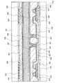
図6(A)にn−層を有する逆スタガ型のTFTの積層構造のモデルを示す。図6(A)に示すように、絶縁表面を有する基板11上にゲート電極12、ゲート絶縁膜13、n−層14、i型の非晶質半導体層15、n+層であるソース領域16、n+層であるドレイン領域17、ソース電極18、ドレイン電極19がそれぞれ設けられている。
FIG. 6A shows a model of a stacked structure of an inverted staggered TFT having an n − layer. As shown in FIG. 6A, a
n−層14を有する逆スタガ型のTFTにおいて、ゲート電極12にしきい値よりも十分に大きい電圧をかけて、オン状態とした場合のドレイン電流の経路10は、まず、ドレイン電極19からn+層であるドレイン領域17、i型の非晶質半導体層15、n−層の順に膜厚方向に第1の電流経路(抵抗Rd)が形成される。
In the inverted staggered TFT having the n − layer 14, when the
そして、i型の非晶質半導体層よりもゲート電極に近い位置にn−層が設けられているため、ゲート絶縁膜13の界面近傍のn−層14をチャネル長方向に第2の電流経路(抵抗Rc(ON))が形成される。
Since the n − layer is provided closer to the gate electrode than the i-type amorphous semiconductor layer, the second current path extends in the channel length direction through the n − layer 14 near the interface of the
そして、n−層からi型の非晶質半導体層15、n+層であるソース領域16、ソース電極18の順に膜厚方向に第3の電流経路(抵抗Rs)が形成される。
Then, a third current path (resistance Rs) is formed in the film thickness direction in the order of the n − layer to the i-type
図6(A)中に示した矢印に相当するドレイン電流の経路10の等価回路は、図6(B)に示す直列接続された複数の抵抗で示すことができる。
An equivalent circuit of the drain
第1の電流経路と第3の電流経路は、膜厚方向の電流経路であるため、約200nm程度の距離である。一方、第2の電流経路は少なくともチャネル長よりも長いため、例えば、約6μm以上となる。また、第1の電流経路(抵抗Rd)は、順方向接続であるため、第2の電流経路(抵抗Rc(ON))及び第3の電流経路(抵抗Rs)に比べて非常に小さい抵抗である。n−層をi型の非晶質半導体層とゲート絶縁膜の間に設けることによって、ゲート絶縁膜界面付近の電気抵抗を低下させ、主なドレイン電流の流れをゲート絶縁膜界面付近に導くことができ、結果としてTFTのオン電流を増大させている。 Since the first current path and the third current path are current paths in the film thickness direction, the distance is about 200 nm. On the other hand, since the second current path is longer than at least the channel length, it is, for example, about 6 μm or more. Further, since the first current path (resistor Rd) is a forward connection, the resistance is very small compared to the second current path (resistor Rc (ON)) and the third current path (resistor Rs). is there. By providing the n − layer between the i-type amorphous semiconductor layer and the gate insulating film, the electrical resistance near the interface of the gate insulating film is lowered, and the main drain current flow is guided near the interface of the gate insulating film. As a result, the on-current of the TFT is increased.
また、逆スタガ型のTFTの製造工程中には、i型の非晶質半導体層の一部(チャネルとなる領域)上の不要なn+層を選択的にエッチングし、さらにオーバーエッチングすることでi型の非晶質半導体層に凹部を形成する。オーバーエッチング後のi型の非晶質半導体層の薄い部分の膜厚が150nm程度以下となると、このバックチャネル側の界面準位の影響でTFTのオン特性が著しく低下する恐れがある。従って、i型の非晶質半導体層は150nmよりも厚い膜厚とする。 In addition, during the manufacturing process of the inverted staggered TFT, an unnecessary n + layer on a part of the i-type amorphous semiconductor layer (a region serving as a channel) is selectively etched and further over-etched. A recess is formed in the i-type amorphous semiconductor layer. If the film thickness of the thin portion of the i-type amorphous semiconductor layer after over-etching is about 150 nm or less, the on-characteristics of the TFT may be significantly deteriorated due to the influence of the interface state on the back channel side. Therefore, the i-type amorphous semiconductor layer has a thickness greater than 150 nm.
また、n−層を有する逆スタガ型のTFTにおいて、オフ状態とした場合、i型の非晶質半導体層の被エッチング部分(ソース電極とドレイン電極の間のバックチャネル界面)を主なドレイン電流の流れとすることができる。i型の非晶質半導体層が150nmよりも厚い膜厚であるため、オフ状態においては、n−層にほとんど電流が流れない。 Further, in an inverted staggered TFT having an n − layer, when turned off, an etched portion of the i-type amorphous semiconductor layer (a back channel interface between the source electrode and the drain electrode) is used as a main drain current. It can be the flow of. Since the i-type amorphous semiconductor layer is thicker than 150 nm, almost no current flows through the n − layer in the off state.
従って、ゲート絶縁膜とi型の非晶質半導体層との間にn−層を有する逆スタガ型のTFTは、オン電流を増加することができ、且つ、十分なオフ電流を有する。 Therefore, an inverted staggered TFT having an n − layer between a gate insulating film and an i-type amorphous semiconductor layer can increase an on-current and has a sufficient off-current.
電界効果移動度に関しては、さらに詳しく考慮する必要がある。ゲート電極に適当な正電位を印加し、ソース電極を接地電位とし、ドレイン電極に正電位を印加した場合(即ちTFTがオン状態の場合)、図6(B)に示す抵抗Rsは、主にソース領域とi型の非晶質半導体層の順方向接続の抵抗値に相当する。また、抵抗Rdは、主に空乏化したn−層の抵抗値に相当し、抵抗Rc(ON)は反転したi型の非晶質半導体層の抵抗値に相当する。 The field effect mobility needs to be considered in more detail. When an appropriate positive potential is applied to the gate electrode, the source electrode is set to the ground potential, and a positive potential is applied to the drain electrode (that is, when the TFT is on), the resistance Rs shown in FIG. This corresponds to the resistance value of the forward connection between the source region and the i-type amorphous semiconductor layer. The resistance Rd mainly corresponds to the resistance value of the depleted n − layer, and the resistance Rc (ON) corresponds to the resistance value of the inverted i-type amorphous semiconductor layer.
なお、反転したi型の非晶質半導体層とは、ゲート電極に電位を印加することで、ゲート絶縁膜との界面に伝導電子が誘起された状態のi型の非晶質半導体層を示す。なお、抵抗Rsは、抵抗Rd及び抵抗Rc(ON)に比べ、非常に小さいと考えられる。 Note that the inverted i-type amorphous semiconductor layer refers to an i-type amorphous semiconductor layer in which conduction electrons are induced at the interface with the gate insulating film by applying a potential to the gate electrode. . Note that the resistance Rs is considered to be very small compared to the resistance Rd and the resistance Rc (ON).
ここで、実際のデバイス構造では、抵抗Rdは、代表的には、厚さ200nm程度のi型の非晶質半導体層で形成される。一方、抵抗Rc(ON)は、代表的には、長さ6μm程度のn−層で形成される。したがって、空乏化したi型の非晶質半導体層の単位長さあたりの抵抗値が、反転したn−層の単位長さあたりの抵抗値の約30倍より大きい(小さい)場合、ドレイン電流に対して、抵抗Rd(抵抗Rc(ON))が支配的になると考えられる。 Here, in an actual device structure, the resistor Rd is typically formed of an i-type amorphous semiconductor layer having a thickness of about 200 nm. On the other hand, the resistor Rc (ON) is typically formed of an n − layer having a length of about 6 μm. Therefore, when the resistance value per unit length of the depleted i-type amorphous semiconductor layer is larger (smaller) than about 30 times the resistance value per unit length of the inverted n − layer, the drain current is On the other hand, it is considered that the resistance Rd (resistance Rc (ON)) becomes dominant.
さて、ゲート電圧を増加していくと、抵抗Rc(ON)は、抵抗Rdより非常に大きい値から、抵抗Rdと同程度の値、抵抗Rdより非常に小さい値になると考えられる。抵抗Rc(ON)が、抵抗Rdより非常に大きい値から、抵抗Rdと同程度の値にかけては、抵抗Rc(ON)の低下に伴い、ドレイン電流は急激に増大していくと考えられる。一方、抵抗Rc(ON)が、抵抗Rdより非常に小さい値になると、もはや、抵抗Rc(ON)が低下しても、ドレイン電流への依存が小さくなる。また、抵抗Rdは、ドレイン電圧を増大するに伴い、抵抗値が下がると考えられる。 As the gate voltage is increased, the resistance Rc (ON) is considered to change from a value that is much larger than the resistance Rd to a value that is comparable to the resistance Rd and much smaller than the resistance Rd. When the resistance Rc (ON) is from a value much larger than the resistance Rd to a value about the same as the resistance Rd, it is considered that the drain current rapidly increases as the resistance Rc (ON) decreases. On the other hand, when the resistance Rc (ON) becomes a value much smaller than the resistance Rd, the dependency on the drain current is reduced even if the resistance Rc (ON) is reduced. Further, the resistance value of the resistor Rd is considered to decrease as the drain voltage increases.
電界効果移動度は、ゲート電圧Vgの増加に対するドレイン電流Idの増加率と考えられる。そこで、上記の内容をまとめると、次のようになる。すなわち、ドレイン電圧が低い(抵抗Rdが高い)場合、ゲート電圧の増加に伴い、電界効果移動度は極大値をもつ。また、ドレイン電圧が高い(抵抗Rdが低い)場合、ゲート電圧の増加に伴い、電界効果移動度は単調増加する。 The field effect mobility is considered to be a rate of increase of the drain current Id with respect to the increase of the gate voltage Vg. Therefore, the above contents are summarized as follows. That is, when the drain voltage is low (the resistance Rd is high), the field effect mobility has a maximum value as the gate voltage increases. In addition, when the drain voltage is high (the resistance Rd is low), the field effect mobility increases monotonously with the increase of the gate voltage.
以上の考察に、ドナー濃度を増大することで、Id曲線が、Vg軸方向にマイナスシフトすることを考慮し、計算を行った結果を図7(A)及び図7(B)に示す。 In consideration of the fact that the Id curve is negatively shifted in the Vg axis direction by increasing the donor concentration, the calculation results are shown in FIGS. 7A and 7B.
なお、計算には、Silvaco社製デバイスシミュレータ”ATLAS”を用い、図6(C)に示すモデルを用いて行っている。計算に用いたアモルファスシリコンのパラメータとしては、エネルギーギャップEg=1.9eV、伝導帯端におけるアクセプタの状態密度nta=7.4E+21 [/eV]、価電子帯におけるドナーの状態密度ntd=7.4E+21 [/eV]、伝導帯端におけるアクセプタの状態密度の減衰係数wta=0.04、価電子帯におけるドナーの状態密度の減衰係数wtd=0.04、ガウシアン分布におけるアクセプタ順位の全状態密度nga=3E+16[/eV]、ガウシアン分布におけるドナー準位の全状態密度ngd=5E+18[/eV]、ガウシアン分布におけるアクセプタ準位のピークのエネルギーega=0.5[eV]、ガウシアン分布におけるドナー準位のピークのエネルギーegd=0.9[eV]、ガウシアン分布におけるアクセプタの全状態密度の減衰係数wga=0.4、ガウシアン分布におけるドナーの全状態密度の減衰係数wgd=0.3とそれぞれ設定した。図6(C)のモデル化は、主に状態密度を定義することで実現した。具体的には、図6(C)のモデルパラメータは、上述のパラメータを適宜定義し、逆スタガ型アモルファスシリコンTFTのDC特性をデバイスシミュレータで計算する。求めた計算値が逆スタガ型アモルファスシリコンTFTの実デバイスのDC特性を十分再現するまで、上述のパラメータを適宜変更して計算を繰り返した。 The calculation is performed using a model shown in FIG. 6C using a device simulator “ATLAS” manufactured by Silvaco. The parameters of the amorphous silicon used for the calculation are energy gap Eg = 1.9 eV, acceptor state density nta = 7.4E + 21 [/ eV], donor state density ntd = 7.4E + 21 in the valence band. [/ EV], acceptor state density attenuation coefficient wta = 0.04 at the conduction band edge, donor state density attenuation coefficient wtd = 0.04 in the valence band, acceptor order total state density nga = in Gaussian distribution 3E + 16 [/ eV], donor state total density ngd = 5E + 18 [/ eV] in Gaussian distribution, acceptor level peak energy in Gaussian distribution ega = 0.5 [eV], donor level in Gaussian distribution Peak energy egd = 0.9 [eV], Gauss The attenuation coefficient wga = 0.4 of the total density of acceptors in the Ann distribution and the attenuation coefficient wgd = 0.3 of the total density of donors in the Gaussian distribution were set. The modeling in FIG. 6C was realized mainly by defining the density of states. Specifically, the model parameters in FIG. 6C define the above-mentioned parameters as appropriate, and the DC characteristics of the inverted staggered amorphous silicon TFT are calculated by a device simulator. The calculation was repeated with the above parameters changed as appropriate until the calculated value sufficiently reproduced the DC characteristics of the actual device of the inverted staggered amorphous silicon TFT.
図6(C)に示すモデルの説明を以下に示す。 The description of the model shown in FIG.
絶縁表面を有する基板11は酸化シリコン(誘電率4.1)を主成分とするガラス基板(厚さ0.5μm)を仮定している。なお、絶縁表面を有する基板11の厚さは、実際の製造工程では0.5mm、0.7mmなどが使われることが多い。絶縁基板の下面における電界が、TFT特性に影響が無い程度に十分厚くなるようにしながら、計算効率を考慮して定義している。
The
絶縁表面を有する基板11上に、アルミニウムとモリブデンとの積層構造(合計厚さ150nm)のゲート電極12を積層している。モリブデンの仕事関数は4.6eVとしている。なお、図6(C)におけるモデル構造では、TFT特性は、ゲート電極の下層材料(ここではアルミニウム)の如何には依存しない。そのため、計算の簡略化のため、モリブデンのみ(厚さ150nm)として計算を行っている。
A
ゲート電極12の上に、窒化シリコン(誘電率7.0、厚さ300nm)のゲート絶縁膜13を積層している。
On the
ゲート絶縁膜13の上に、a−Si(n−)で表記するn−層20(それぞれ、厚さ10nm、20nm、50nmの条件として条件振りを行い、ドナー濃度1×1015cm−3〜5×1017cm−3でそれぞれ条件振りを行っている)を積層している。さらにその上に、第3のa−Si(i)で表記する第3のi層21c(それぞれ厚さ90nm、80nm、50nmで条件振りを行っている)を積層している。
On the
また、第3のi層21cの上に、一方の側に第1のa−Si(i)で表記する第1のi層21a(厚さ50nm)を積層し、もう一方の側に第2のa−Si(i)で表記する第2のi層21b(厚さ50nm)を積層している。
In addition, a
第1のa−Si(i)上に第1のa−Si(n+)であるソース領域16(厚さ50nm)を積層し、第2のa−Si(i)上に、第2のa−Si(n+)であるドレイン領域17(厚さ50nm)を積層している。 A source region 16 (thickness: 50 nm) which is the first a-Si (n +) is stacked on the first a-Si (i), and the second a-Si (i) is stacked on the second a-Si (i). A drain region 17 (thickness: 50 nm) which is -Si (n +) is stacked.
図6(C)において、ソース領域16とドレイン領域17との距離が、TFTのチャネル長Lになる。ここでは、チャネル長L=6[μm]としている。また、ソース領域16及びドレイン領域17のドナー濃度は1×1019cm−3としており、高い導電性を有する。
In FIG. 6C, the distance between the
ソース領域16と第2のドレイン領域17との上に、モリブデンとアルミニウムとの積層構造(厚さ300nm)のソース電極18とドレイン電極19とを各々積層している。モリブデンとソース領域16及びドレイン領域17との間は、オーミック接触を仮定している。なお、図6(C)におけるデバイス構造のTFT特性は、ソース電極とドレイン電極との上層材料(ここではアルミニウム)の如何には依存しない。そのため、計算の簡略化のため、ソース電極とドレイン電極とは、モリブデンのみ(厚さ300nm)として計算を行っている。
On the
図7(A)は、ドレイン電圧が低い(Vd=1V)場合のn−層のドナー濃度と最大移動度の関係を示すグラフである。最大移動度(最大電界効果移動度)は、移動度(電界効果移動度)の最大値で定義する。図7(A)においては、ドナー濃度が増大するにつれ、最大移動度が増大している。不純物を添加する半導体層の膜厚を増大することで、伝導に寄与する半導体層が増大する。したがって、移動度が増大することになる。アモルファス状態であるn−層の抵抗が高いため、相対的に、抵抗Rdが抵抗Rc(ON)より低くなるためと考えられる。 FIG. 7A is a graph showing the relationship between the donor concentration of the n − layer and the maximum mobility when the drain voltage is low (Vd = 1 V). The maximum mobility (maximum field effect mobility) is defined by the maximum value of mobility (field effect mobility). In FIG. 7A, the maximum mobility increases as the donor concentration increases. By increasing the thickness of the semiconductor layer to which the impurity is added, the number of semiconductor layers contributing to conduction increases. Therefore, the mobility increases. This is probably because the resistance of the n − layer in the amorphous state is high, and thus the resistance Rd is relatively lower than the resistance Rc (ON).
図7(B)は、ドレイン電圧が高い(Vd=14V)場合のn−層のドナー濃度と最大移動度の関係を示すグラフである。図7(B)においては、ドナー濃度が増大するにつれ、最大移動度が向上している。これは、上述のドレイン電圧が高い場合の考察に、不純物添加によるしきい値電圧のマイナスシフトを考慮すれば、説明できる。 FIG. 7B is a graph showing the relationship between the donor concentration of the n − layer and the maximum mobility when the drain voltage is high (Vd = 14 V). In FIG. 7B, the maximum mobility is improved as the donor concentration is increased. This can be explained by considering the negative shift of the threshold voltage due to the addition of impurities in consideration of the case where the drain voltage is high.
また、逆スタガ型のTFTは、リンが十分に活性化する熱処理を行わないため、含まれているリン原子が全てドナーとして働くわけではなく、ドナーとして寄与するのはリン原子数の内の約1%〜5%、代表的には3%である。 In addition, since the reverse stagger type TFT does not perform heat treatment that sufficiently activates phosphorus, not all of the contained phosphorus atoms serve as donors, and the donor contributes about the number of phosphorus atoms. 1% to 5%, typically 3%.
なお、デバイスシミュレータを用いた計算は、均一のドナー濃度を有する層を仮定して行っている。 Note that the calculation using the device simulator is performed assuming a layer having a uniform donor concentration.
また、n−層として機能するのであれば、特に均一のリン濃度を含む層となっていなくともよい。むしろ、ゲート絶縁膜の界面にリンの濃度ピークが位置するような濃度勾配を有するn−層とすることが好ましい。リンの濃度ピークが界面から離れ、n+層に近づくに従って、オフ電流の増大を招くこととなるからである。 Moreover, as long as it functions as an n − layer, it does not have to be a layer containing a particularly uniform phosphorus concentration. Rather, an n − layer having a concentration gradient such that a phosphorus concentration peak is located at the interface of the gate insulating film is preferable. This is because the off-current increases as the phosphorus concentration peak moves away from the interface and approaches the n + layer.
なお、本明細書において、i型の非晶質半導体とは、実質的に真性な半導体であって、含まれるp型若しくはn型を付与する不純物が1×1020cm−3以下、且つ、リン濃度がリンのSIMS分析の下限である6×1015cm−3未満の濃度であり、且つ、酸素及び窒素が9×1019cm−3以下の濃度であり、暗伝導度に対して光伝導度が100倍以上である半導体を指す。 Note that in this specification, an i-type amorphous semiconductor is a substantially intrinsic semiconductor, and an impurity imparting p-type or n-type contained therein is 1 × 10 20 cm −3 or less, and The phosphorus concentration is less than 6 × 10 15 cm −3, which is the lower limit of the SIMS analysis of phosphorus, and oxygen and nitrogen are concentrations of 9 × 10 19 cm −3 or less. A semiconductor whose conductivity is 100 times or more.
また、本明細書において、n−層とは、リンのSIMS分析の下限である6×1015cm−3以上のリン濃度を有し、3×1018cm−3以下の濃度範囲、且つ、p型を付与する不純物濃度が、同じ層中に含まれるリン濃度の10分の1未満の非晶質半導体層と定義する。 In the present specification, the n − layer has a phosphorus concentration of 6 × 10 15 cm −3 or more which is the lower limit of the SIMS analysis of phosphorus, a concentration range of 3 × 10 18 cm −3 or less, and It is defined as an amorphous semiconductor layer in which the impurity concentration imparting p-type is less than one-tenth of the phosphorus concentration contained in the same layer.
また、本明細書において、n型半導体層とは、n型を付与する不純物が1×10¹⁹/cm3以上の濃度を含み、導電性を示す微結晶半導体層または非晶質半導体層と定義する。 Further, in this specification, an n-type semiconductor layer is defined as a microcrystalline semiconductor layer or an amorphous semiconductor layer which has a concentration of an impurity imparting n-type conductivity of 1 × 10 19 / cm 3 or more and exhibits conductivity. To do.
また、本明細書における濃度は、SIMS(二次イオン質量分析計)を用いた分析による濃度のピーク値を指している。SIMSは濃度の低い側から高い側に向かって深さ方向に分析された値である。本明細書において、ゲート絶縁膜側から非晶質半導体層側に向けて深さ方向にSIMS分析を行うことが好ましい。 In addition, the concentration in the present specification indicates a peak value of concentration obtained by analysis using SIMS (secondary ion mass spectrometer). SIMS is a value analyzed in the depth direction from the lower concentration side to the higher side. In this specification, SIMS analysis is preferably performed in the depth direction from the gate insulating film side toward the amorphous semiconductor layer side.
逆スタガ型のTFTにおいて、i型の非晶質シリコン層とゲート絶縁膜との間に薄いn−層を設けることにより、TFTの電界効果移動度を向上させることができる。また、効率よく微結晶半導体膜の成膜を行うことができる。 In a reverse stagger type TFT, by providing a thin n − layer between an i-type amorphous silicon layer and a gate insulating film, the field effect mobility of the TFT can be improved. Further, the microcrystalline semiconductor film can be efficiently formed.
本発明の実施形態及び実施例について、以下に説明する。 Embodiments and examples of the present invention will be described below.
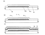
(実施の形態1)
本実施の形態では、液晶表示装置に用いられる薄膜トランジスタの作製工程について、図1乃至図4を用いて説明する。図1乃至図3は、薄膜トランジスタの作製工程を示す断面図であり、図4は、一画素における薄膜トランジスタ及び画素電極の接続領域の上面図である。
(Embodiment 1)
In this embodiment, a manufacturing process of a thin film transistor used for a liquid crystal display device will be described with reference to FIGS. 1 to 3 are cross-sectional views illustrating a manufacturing process of a thin film transistor, and FIG. 4 is a top view of a connection region between a thin film transistor and a pixel electrode in one pixel.
図1(A)に示すように、基板50上に金属層の積層からなるゲート電極を形成する。
As shown in FIG. 1A, a gate electrode formed by stacking metal layers is formed over a
基板50は、バリウムホウケイ酸ガラス、アルミノホウケイ酸ガラス、若しくはアルミノシリケートガラスなど、フュージョン法やフロート法で作製される無アルカリガラス基板、セラミック基板の他、本作製工程の処理温度に耐えうる耐熱性を有するプラスチック基板等を用いることができる。また、ステンレス合金などの金属基板の表面に絶縁膜を設けた基板を適用しても良い。基板50がマザーガラスの場合、基板の大きさは、第1世代(例えば、320mm×400mm)、第2世代(例えば、400mm×500mm)、第3世代(例えば、550mm×650mm)、第4世代(例えば、680mm×880mm、または730mm×920mm)、第5世代(例えば、1000mm×1200mmまたは1100mm×1300mm)、第6世代(例えば、1500mm×1800mm)、第7世代(例えば、1900mm×2200mm)、第8世代(例えば、2160mm×2460mm)、第9世代(例えば、2400mm×2800mm)、第10世代(例えば、2850mm×3050mm)等を用いることができる。
The
ゲート電極は、チタン、モリブデン、クロム、タンタル、タングステン、アルミニウムなどの金属材料またはその合金材料を用いて形成する。ゲート電極は、スパッタリング法で基板50上に導電膜を形成し、当該導電膜上にフォトリソグラフィ技術またはインクジェット法によりマスクを形成し、当該マスクを用いて導電膜をエッチングすることで、形成することができる。また、銀、金、銅などの導電性ナノペーストを用いてインクジェット法により吐出し焼成して、ゲート電極を形成することもできる。なお、ゲート電極と基板50の密着性向上と下地への拡散を防ぐバリアメタルとして、上記金属材料の窒化物膜を、基板50及びゲート電極の間に設けてもよい。ここでは、第1のフォトマスクを用いて形成したレジストマスクを用いて基板50上に形成された積層膜をエッチングしてゲート電極を形成する。
The gate electrode is formed using a metal material such as titanium, molybdenum, chromium, tantalum, tungsten, or aluminum, or an alloy material thereof. The gate electrode is formed by forming a conductive film on the
具体的なゲート電極構造の例としては、第1の導電層51aとなるアルミニウム膜上に第2の導電層51bとなるモリブデン膜を積層させ、アルミニウム特有のヒロックやエレクトロマイグレーションを防ぐ構造にしてもよい。本実施の形態では、大面積の基板を用いて表示画面が大きい表示装置を作製する例であるので、電気抵抗の低いアルミニウムからなる第1の導電層51aと、第1の導電層51aよりも耐熱性の高い第2の導電層51bとを積層させたゲート電極とする。また、アルミニウム膜をモリブデン膜で挟んだ3層構造としてもよい。また、他のゲート電極構造の例として、銅膜上にモリブデン膜の積層、銅膜上に窒化チタン膜の積層、銅膜上に窒化タンタル膜の積層が挙げられる。
As a specific example of the gate electrode structure, a molybdenum film serving as the second
なお、ゲート電極上には半導体膜や配線を形成するので、段切れ防止のため端部がテーパー状になるように加工することが望ましい。また、図示しないがこの工程でゲート電極に接続する配線も同時に形成することができる。 Note that since a semiconductor film or a wiring is formed over the gate electrode, it is preferable to process the end portion to be tapered in order to prevent disconnection. Although not shown, a wiring connected to the gate electrode can be formed at the same time in this step.
次に、ゲート電極の上層である第2の導電層51b上に、ゲート絶縁膜52を形成する。
Next, the
ゲート絶縁膜52はCVD法やスパッタリング法等を用いて、窒化シリコン膜、または窒化酸化シリコン膜で形成することができる。ゲート絶縁膜に形成されるピンホール等による層間ショートを防ぐため、異なる絶縁層を用いて多層とすることが好ましい。ここでは、ゲート絶縁膜52として、窒化シリコン膜を形成する形態を示す。ここまでの工程を終えた断面図が図1(A)に相当する。
The
ここでは、窒化酸化シリコン膜とは、その組成として、酸素よりも窒素の含有量が多いものであって、濃度範囲として酸素が15〜30原子%、窒素が20〜35原子%、Siが25〜35原子%、水素が15〜25原子%の範囲で含まれるものをいう。 Here, the silicon nitride oxide film has a composition containing more nitrogen than oxygen, and the concentration ranges of oxygen are 15 to 30 atomic%, nitrogen is 20 to 35 atomic%, and Si is 25. -35 atomic%, and hydrogen is included in the range of 15-25 atomic%.
次いで、ゲート絶縁膜の成膜後、大気に触れさせることなく基板を搬送し、ゲート絶縁膜を成膜する真空チャンバーとは異なる真空チャンバーで非晶質半導体膜を成膜する。 Next, after the gate insulating film is formed, the substrate is transferred without being exposed to the air, and an amorphous semiconductor film is formed in a vacuum chamber different from the vacuum chamber in which the gate insulating film is formed.
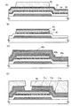
基板を反応室に搬入する前に、水素または希ガスを導入してプラズマを発生させて反応室の内壁に付着した気体(酸素及び窒素などの大気成分、若しくは反応室のクリーニングに使用したエッチングガス)を除去した後、水素とシランガスと微量のホスフィン(PH3)ガスを導入する。シランガスは、反応室内の酸素、水分等と反応させることができる。微量のホスフィンガスは、後に成膜される非晶質シリコン膜中にリンを含ませることができる。 Before introducing the substrate into the reaction chamber, hydrogen or a rare gas is introduced to generate plasma, and gas attached to the inner wall of the reaction chamber (atmospheric components such as oxygen and nitrogen, or etching gas used for cleaning the reaction chamber) ), Hydrogen, silane gas, and a small amount of phosphine (PH 3 ) gas are introduced. Silane gas can be reacted with oxygen, moisture and the like in the reaction chamber. A trace amount of phosphine gas can contain phosphorus in an amorphous silicon film to be formed later.
次いで、基板を反応室に搬入して、図1(B)に示すように、シランガス及び微量のホスフィンガスに曝した後、非晶質シリコン膜を成膜する。非晶質シリコン膜は、代表的には、SiH4、Si2H6などの水素化珪素を水素で希釈してプラズマ生成することで成膜することができる。水素化珪素の流量の1倍以上10倍以下、更に好ましくは1倍以上5倍以下の流量の水素を用いて、水素を含む非晶質シリコンを形成することができる。 Next, the substrate is carried into a reaction chamber and exposed to silane gas and a small amount of phosphine gas as shown in FIG. 1B, and then an amorphous silicon film is formed. The amorphous silicon film can be typically formed by generating plasma by diluting silicon hydride such as SiH 4 or Si 2 H 6 with hydrogen. Amorphous silicon containing hydrogen can be formed using hydrogen at a flow rate of 1 to 10 times, more preferably 1 to 5 times the flow rate of silicon hydride.
また、上記手順により、ゲート絶縁膜界面近傍の非晶質シリコン膜にリンを含有させてn型化させることができる。従って、図1(C)に示すように、n型化された非晶質シリコン膜53と、i型の非晶質シリコン膜54との積層が形成される。図1(C)には、n型化された非晶質シリコン膜53と、i型の非晶質シリコン膜54との界面を分かりやすくするため図示したが、実際にはリンの濃度がゲート絶縁膜界面から離れる距離の増大に従って減少する。
Further, by the above procedure, the amorphous silicon film near the interface of the gate insulating film can be made n-type by containing phosphorus. Accordingly, as shown in FIG. 1C, a stack of the n-type
また、上記手順により酸素だけでなく、窒素、及び炭素が非晶質シリコン膜とゲート絶縁膜との界面近傍に混入する濃度を低減することができる。 Further, the concentration of not only oxygen but also nitrogen and carbon near the interface between the amorphous silicon film and the gate insulating film can be reduced by the above procedure.
次いで、i型の非晶質シリコン膜54の成膜後、大気に触れさせることなく基板を搬送し、i型の非晶質シリコン膜を成膜する真空チャンバーとは異なる真空チャンバーで一導電型を付与する不純物が添加された半導体膜55を成膜することが好ましい。
Next, after forming the i-type
一導電型を付与する不純物が添加された半導体膜55は、代表的な不純物元素としてリンを添加すれば良く、水素化珪素にホスフィンガスなどの不純物気体を加えれば良い。一導電型を付与する不純物が添加された半導体膜55は2nm以上50nm以下の厚さで形成する。一導電型を付与する不純物が添加された半導体膜の膜厚を、薄くすることでスループットを向上させることができる。
In the
次いで、図2(A)に示すように、一導電型を付与する不純物が添加された半導体膜55上にレジストマスク56を形成する。レジストマスク56は、フォトリソグラフィ技術またはインクジェット法により形成する。ここでは、第2のフォトマスクを用いて、一導電型を付与する不純物が添加された半導体膜55上に塗布されたレジストを露光現像して、レジストマスク56を形成する。
Next, as illustrated in FIG. 2A, a resist
次いで、レジストマスク56を用いてn型化された非晶質シリコン膜53、i型の非晶質シリコン膜54、及び導電型を付与する不純物が添加された半導体膜55をエッチングして、図2(B)に示すように、n型化された非晶質シリコン膜61、i型の非晶質シリコン膜62、及び一導電型を付与する不純物が添加された半導体膜63を形成する。この後、レジストマスク56を除去する。
Next, the n-type
n型化された非晶質シリコン膜61、i型の非晶質シリコン膜62の端部側面が傾斜していることにより、i型の非晶質シリコン膜62上に形成されるソース領域及びドレイン領域とn型化された非晶質シリコン膜61との間にリーク電流が生じることを防止することが可能である。また、ソース電極及びドレイン電極と、n型化された非晶質シリコン膜61との間にリーク電流が生じるのを防止することが可能である。n型化された非晶質シリコン膜61及びi型の非晶質シリコン膜62の端部側面の傾斜角度は、30°〜90°、好ましくは45°〜80°である。このような角度とすることで、段差形状によるソース電極またはドレイン電極の段切れを防ぐことができる。
Since the end side surfaces of the n-type
次に、図2(C)に示すように、一導電型を付与する不純物が添加された半導体膜63及びゲート絶縁膜52を覆うように導電膜として導電膜65a〜65cを形成する。導電膜65a〜65cは、アルミニウム、銅、若しくはシリコン、チタン、ネオジム、スカンジウム、モリブデンなどの耐熱性向上元素若しくはヒロック防止元素が添加されたアルミニウム合金の単層または積層で形成することが好ましい。また、一導電型を付与する不純物が添加された半導体膜と接する側の膜を、チタン、タンタル、モリブデン、タングステン、またはこれらの元素の窒化物で形成し、その上にアルミニウムまたはアルミニウム合金を形成した積層構造としても良い。更には、アルミニウムまたはアルミニウム合金の上面及び下面を、チタン、タンタル、モリブデン、タングステン、またはこれらの元素の窒化物で挟んだ積層構造としてもよい。ここでは、導電膜としては、導電膜65a〜65cの3層が積層した構造の導電膜を示し、導電膜65a、65cにモリブデン膜、導電膜65bにアルミニウム膜を用いた積層導電膜を示す。導電膜65a〜65cは、スパッタリング法や真空蒸着法で形成する。
Next, as illustrated in FIG. 2C,
次に、図2(D)に示すように、導電膜65a〜65c上に第3のフォトマスクを用いてレジストマスク66を形成し、導電膜65a〜65cの一部をエッチングしてソース電極及びドレイン電極71a〜71cを形成する。導電膜65a〜65cをウエットエッチングすると、導電膜65a〜65cの端部が選択的にエッチングされる。この結果、導電膜を等方的にエッチングするため、レジストマスク66より面積の小さいソース電極及びドレイン電極71a〜71cを形成することができる。
Next, as illustrated in FIG. 2D, a resist
次に、図3(A)に示すように、レジストマスク66を用いて一導電型を付与する不純物が添加された半導体膜63をエッチングして、一対のソース領域及びドレイン領域72を形成する。さらに、当該エッチング工程において、i型の非晶質シリコン膜62の一部もエッチングする。一部エッチングされた、窪み(溝)が形成されたi型の非晶質シリコン膜をi型の非晶質シリコン膜73と示す。ソース領域及びドレイン領域と、i型の非晶質シリコン膜の窪み(溝)とを同一工程で形成することができる。i型の非晶質シリコン膜の窪み(溝)の深さをi型の非晶質シリコン膜の一番膜厚の厚い領域の1/2〜1/3とすることで、ソース領域及びドレイン領域の距離を離すことが可能であるため、ソース領域及びドレイン領域の間でのリーク電流を低減することができる。この後、レジストマスク66を除去する。
Next, as illustrated in FIG. 3A, the
特にドライエッチングなどで用いるプラズマに曝されるとレジストマスクは変質し、レジスト除去工程で完全には除去されず、残渣が残ることを防ぐためにi型の非晶質シリコン膜を50nm程度エッチングする。レジストマスク66は、導電膜65a〜65cの一部のエッチング処理と、ソース領域及びドレイン領域72の形成時のエッチング処理の2回に用いられており、どちらもドライエッチングを用いる場合には、残渣が残りやすいため、残渣を完全に除去する際にエッチングされてもよいi型の非晶質シリコン膜の膜厚を厚く形成することは有効である。
In particular, when exposed to plasma used in dry etching or the like, the resist mask changes in quality and is not completely removed in the resist removing process, and the i-type amorphous silicon film is etched by about 50 nm in order to prevent residues from remaining. The resist
次に、図3(B)に示すように、ソース電極及びドレイン電極71a〜71c、ソース領域及びドレイン領域72、i型の非晶質シリコン膜73、n型化された非晶質シリコン膜61、及びゲート絶縁膜52を覆う絶縁膜76を形成する。絶縁膜76は、ゲート絶縁膜52と同じ成膜方法を用いて形成することができる。なお、絶縁膜76は、大気中に浮遊する有機物や金属物、水蒸気などの汚染不純物の侵入を防ぐためのものであり、緻密な膜が好ましい。また、絶縁膜76に窒化シリコン膜を用いることで、i型の非晶質シリコン膜73中の酸素濃度を5×10¹⁹atoms/cm3以下、好ましくは1×1019atoms/cm3以下とすることができる。
Next, as shown in FIG. 3B, source and
図3(B)に示すように、ソース電極及びドレイン電極71a〜71cの端部と、ソース領域及びドレイン領域72の端部は一致せず、端部の位置がずれた形状となることで、ソース電極及びドレイン電極71a〜71cの端部の距離が離れるため、ソース電極及びドレイン電極間のリーク電流やショートを防止することができる。また、ソース電極及びドレイン電極71a〜71cの端部と、ソース領域及びドレイン領域72の端部は一致せずずれた形状であるため、ソース電極及びドレイン電極71a〜71c及びソース領域及びドレイン領域72の端部に電界が集中せず、ゲート電極と、ソース電極及びドレイン電極71a〜71cとの間でのリーク電流を防止することができる。このため、信頼性が高く、且つ耐圧の高い薄膜トランジスタを作製することができる。
As shown in FIG. 3B, the end portions of the source and
以上の工程により、薄膜トランジスタ74を形成することができる。
Through the above process, the
本実施の形態で示す薄膜トランジスタは、ゲート電極上にゲート絶縁膜、n型化された非晶質シリコン膜、i型の非晶質シリコン膜、ソース領域及びドレイン領域、ソース電極及びドレイン電極が積層される。また、i型の非晶質シリコン膜の一部には窪み(溝)が形成されており、当該窪み以外の領域がソース領域及びドレイン領域で覆われる。即ち、i型の非晶質シリコン膜に形成される窪みにより、ソース領域及びドレイン領域の距離が離れているため、ソース領域及びドレイン領域の間でのリーク電流を低減することができる。また、i型の非晶質シリコン膜の一部をエッチングすることにより窪みを形成するため、ソース領域及びドレイン領域の形成工程において発生するエッチング残渣を除去することができるため、残渣を介してソース領域及びドレイン領域にリーク電流(寄生チャネル)が発生することを回避することができる。 In the thin film transistor described in this embodiment, a gate insulating film, an n-type amorphous silicon film, an i-type amorphous silicon film, a source region and a drain region, a source electrode and a drain electrode are stacked over a gate electrode. Is done. A depression (groove) is formed in a part of the i-type amorphous silicon film, and regions other than the depression are covered with the source region and the drain region. That is, since the distance between the source region and the drain region is increased due to the depression formed in the i-type amorphous silicon film, leakage current between the source region and the drain region can be reduced. In addition, since a depression is formed by etching a part of the i-type amorphous silicon film, an etching residue generated in the formation process of the source region and the drain region can be removed. Generation of a leakage current (parasitic channel) in the region and the drain region can be avoided.
次に、絶縁膜76上に平坦化膜82を形成する。平坦化膜82は有機樹脂膜で形成する。次いで、第4のフォトマスクを用いて形成したレジストマスクを用いて絶縁膜76の一部及び平坦化膜82をエッチングしてコンタクトホールを形成し、当該コンタクトホールにおいてソース電極またはドレイン電極71cに接する画素電極77を形成する。なお、図3(C)は、図4の鎖線A−Bの断面図に相当する。
Next, a
図4に示すように、ソース領域及びドレイン領域72の端部は、ソース電極及びドレイン電極71cの端部の外側に位置することが分かる。また、i型の非晶質シリコン膜73の端部はソース電極及びドレイン電極71c及びソース領域及びドレイン領域72の端部の外側に位置する。また、ソース電極及びドレイン電極の一方はソース電極及びドレイン電極の他方を囲む形状(具体的には、U字型、C字型)である。このため、キャリアが移動する領域の面積を増加させることが可能であるため、電流量を増やすことが可能であり、薄膜トランジスタの面積を縮小することができる。なお、ソース電極またはドレイン電極の一方は、ソース配線またはドレイン配線としても機能する。
As shown in FIG. 4, it can be seen that the end portions of the source and drain
また、画素電極77は、酸化タングステンを含むインジウム酸化物、酸化タングステンを含むインジウム亜鉛酸化物、酸化チタンを含むインジウム酸化物、酸化チタンを含むインジウム錫酸化物、インジウム錫酸化物、インジウム亜鉛酸化物、酸化シリコンを添加したインジウム錫酸化物などの透光性を有する導電性材料を用いることができる。
The
また、画素電極77として、導電性高分子(導電性ポリマーともいう)を含む導電性組成物を用いて形成することができる。導電性組成物を用いて形成した画素電極は、シート抵抗が10000Ω/□以下、波長550nmにおける透光率が70%以上であることが好ましい。シート抵抗は、より低いことが好ましい。また、導電性組成物に含まれる導電性高分子の抵抗率が0.1Ω・cm以下であることが好ましい。
The
導電性高分子としては、いわゆるπ電子共役系導電性高分子を用いることができる。例えば、ポリアニリンまたはその誘導体、ポリピロールまたはその誘導体、ポリチオフェンまたはその誘導体、若しくはこれらの2種以上の共重合体などがあげられる。 As the conductive polymer, a so-called π-electron conjugated conductive polymer can be used. For example, polyaniline or a derivative thereof, polypyrrole or a derivative thereof, polythiophene or a derivative thereof, or a copolymer of two or more kinds thereof can be given.
ここでは、画素電極77としては、スパッタリング法によりインジウム錫酸化物膜を成膜した後、インジウム錫酸化物膜上にレジストを塗布する。次に、第5のフォトマスクを用いてレジストを露光及び現像し、レジストマスクを形成する。次に、レジストマスクを用いてインジウム錫酸化物膜をエッチングして画素電極77を形成する。
Here, as the
以上により表示装置に用いることが可能な素子基板を形成することができる。 Through the above steps, an element substrate that can be used for a display device can be formed.
(実施の形態2)
実施の形態1は、シランガス及び微量のホスフィンガスに曝した後、非晶質シリコン膜を成膜することによってn型化された非晶質シリコン膜と、i型の非晶質シリコン膜との積層を形成する例を示したが、特に限定されず、ゲート絶縁膜を積層構造として下層にリンを含ませることによって、その上方にi型の非晶質シリコン膜を成膜し、ゲート絶縁膜の界面付近にn型化された非晶質シリコン膜が形成される方法を用いてもよい。その例を図5を用いて説明する。
(Embodiment 2)
In Embodiment 1, an amorphous silicon film formed by forming an amorphous silicon film after being exposed to a silane gas and a small amount of phosphine gas, and an i-type amorphous silicon film Although an example of forming a stack is shown, the gate insulating film is not particularly limited, and an i-type amorphous silicon film is formed thereon by including phosphorus in the lower layer with the gate insulating film as a stacked structure, and the gate insulating film Alternatively, a method of forming an n-type amorphous silicon film in the vicinity of the interface may be used. An example of this will be described with reference to FIG.
本明細書で開示する他の作製方法に関する構成は、絶縁表面を有する基板上にゲート電極を形成し、ゲート電極上にリンを含む絶縁層を形成し、リンを含む絶縁層上にn型非晶質半導体層と、n型非晶質半導体層上にn型非晶質半導体層よりも膜厚の厚い非晶質半導体層を形成し、非晶質半導体層上にn型非晶質半導体層に含まれるリンの濃度よりも高濃度のリンを含むn型半導体層を形成し、n型半導体層上にソース電極またはドレイン電極を形成する半導体装置の作製方法である。 In another structure disclosed in this specification, a gate electrode is formed over a substrate having an insulating surface, an insulating layer including phosphorus is formed over the gate electrode, and the n-type non-contact layer is formed over the insulating layer including phosphorus. A crystalline semiconductor layer, an amorphous semiconductor layer thicker than the n-type amorphous semiconductor layer is formed on the n-type amorphous semiconductor layer, and the n-type amorphous semiconductor is formed on the amorphous semiconductor layer This is a method for manufacturing a semiconductor device in which an n-type semiconductor layer containing phosphorus at a concentration higher than the concentration of phosphorus contained in a layer is formed, and a source electrode or a drain electrode is formed over the n-type semiconductor layer.
実施の形態1と同様にゲート電極を形成する。その後、第1のゲート絶縁膜67を形成し、第2のゲート絶縁膜68を形成する。第1のゲート絶縁膜67としてはリンを含む窒化シリコン膜またはリンを含む酸化窒化シリコン膜を用いる。酸化窒化シリコン膜とは、その組成として、窒素よりも酸素の含有量が多いものであって、濃度範囲として酸素が55〜65原子%、窒素が1〜20原子%、Siが25〜35原子%、水素が0.1〜10原子%の範囲で含まれるものをいう。
A gate electrode is formed as in the first embodiment. Thereafter, a first
ここでは、第1のゲート絶縁膜67としてシランガス30sccm、N2Oガス1200sccm、ホスフィンガスを水素で0.5%に希釈したガスを60sccmとして成膜を行い、膜厚を10nmとする。また、第2のゲート絶縁膜68の膜厚は100nmとする。なお、明瞭に示すため、第2のゲート絶縁膜68の膜厚を厚く図示しており、図面での膜厚比は異ならせている。
Here, the first
次いで、大気に触れることなく非晶質シリコン膜を成膜すると、非晶質シリコン膜にもリンを含ませることができる。こうして、n型化された非晶質シリコン膜と、i型の非晶質シリコン膜との積層を形成することができる。以降の工程は、実施の形態1と同様に行えばよい。 Next, when an amorphous silicon film is formed without exposure to the air, the amorphous silicon film can also contain phosphorus. Thus, a stacked layer of the n-type amorphous silicon film and the i-type amorphous silicon film can be formed. The subsequent steps may be performed in the same manner as in the first embodiment.
また、実施の形態1と同様に、継続してホスフィンを供給しているわけではないため、ゲート絶縁膜近傍にリンの濃度ピークが位置する深さ方向の濃度プロファイルを示す。 Further, as in Embodiment 1, since phosphine is not continuously supplied, a concentration profile in the depth direction in which a phosphorus concentration peak is located in the vicinity of the gate insulating film is shown.
(実施の形態3)
実施の形態1は、シランガス及び微量のホスフィンガスに曝した後、非晶質シリコン膜を成膜することによってn型化された非晶質シリコン膜と、i型の非晶質シリコン膜との積層を形成する例を示したが、特に限定されず、ゲート絶縁膜を形成する前にチャンバー内壁にリンを含む非晶質シリコン膜を成膜しておくことで、n型化された非晶質シリコン膜と、i型の非晶質シリコン膜との積層を形成してもよい。
(Embodiment 3)
In Embodiment 1, an amorphous silicon film formed by forming an amorphous silicon film after being exposed to a silane gas and a small amount of phosphine gas, and an i-type amorphous silicon film Although an example of forming a stack is shown, it is not particularly limited, and an amorphous silicon film containing phosphorus is formed on the inner wall of the chamber before forming a gate insulating film, thereby forming an n-type amorphous film. A stack of a crystalline silicon film and an i-type amorphous silicon film may be formed.
本明細書で開示する他の作製方法に関する構成は、絶縁表面を有する基板上にゲート電極を形成し、ゲート電極を形成した基板をチャンバー内壁にリンを含む半導体膜が形成されたチャンバー内で絶縁層とn型非晶質半導体層と、n型非晶質半導体層上にn型非晶質半導体層よりも膜厚の厚い非晶質半導体層を形成し、非晶質半導体層上にn型非晶質半導体層に含まれるリンの濃度よりも高濃度のリンを含むn型半導体層を形成した後、チャンバーから搬出し、n型半導体層上にソース電極またはドレイン電極を形成する半導体装置の作製方法である。 In another structure disclosed in this specification, a gate electrode is formed over a substrate having an insulating surface, and the substrate on which the gate electrode is formed is insulated in a chamber in which a semiconductor film containing phosphorus is formed on the inner wall of the chamber. Forming an n-type amorphous semiconductor layer, an amorphous semiconductor layer thicker than the n-type amorphous semiconductor layer on the n-type amorphous semiconductor layer, and forming an n-type amorphous semiconductor layer on the amorphous semiconductor layer Semiconductor device in which an n-type semiconductor layer containing phosphorus at a concentration higher than the concentration of phosphorus contained in a p-type amorphous semiconductor layer is formed and then removed from the chamber to form a source electrode or a drain electrode on the n-type semiconductor layer This is a manufacturing method.
実施の形態1と同様にゲート電極を形成する。その後、チャンバー内壁に50nm程度のリンを含む非晶質シリコン膜を成膜する。次いで、実施の形態1と同様にゲート絶縁膜を形成する。次いで、大気に触れることなく非晶質シリコン膜を成膜すると、非晶質シリコン膜にもリンを含ませることができる。こうして、n型化された非晶質シリコン膜と、i型の非晶質シリコン膜との積層を形成することができる。 A gate electrode is formed as in the first embodiment. Thereafter, an amorphous silicon film containing phosphorus of about 50 nm is formed on the inner wall of the chamber. Next, a gate insulating film is formed as in the first embodiment. Next, when an amorphous silicon film is formed without exposure to the air, the amorphous silicon film can also contain phosphorus. Thus, a stacked layer of the n-type amorphous silicon film and the i-type amorphous silicon film can be formed.
さらに、同一チャンバーを用いてi型の非晶質シリコン膜上に高濃度のリンを含む第2のn型非晶質半導体層を形成した後、チャンバーから搬出する。第2のn型非晶質半導体層を形成した際には再びチャンバー内壁にリンを含む非晶質シリコン膜が成膜されるため、引き続き次の基板を処理することもできる。以降の工程は、実施の形態1と同様に行えばよい。 Further, after forming a second n-type amorphous semiconductor layer containing high-concentration phosphorus on the i-type amorphous silicon film using the same chamber, the second n-type amorphous semiconductor layer containing the high-concentration phosphorus is removed from the chamber. When the second n-type amorphous semiconductor layer is formed, an amorphous silicon film containing phosphorus is formed again on the inner wall of the chamber, so that the next substrate can be processed subsequently. The subsequent steps may be performed in the same manner as in the first embodiment.
また、実施の形態1と同様に、継続してホスフィンを供給しているわけではないため、ゲート絶縁膜近傍にリンの濃度ピークが位置する深さ方向の濃度プロファイルを示す。 Further, as in Embodiment 1, since phosphine is not continuously supplied, a concentration profile in the depth direction in which a phosphorus concentration peak is located in the vicinity of the gate insulating film is shown.
このように、様々な方法で、n型化された非晶質シリコン膜と、i型の非晶質シリコン膜との積層を形成することができる。 In this manner, a stack of the n-type amorphous silicon film and the i-type amorphous silicon film can be formed by various methods.
(実施の形態4)
実施の形態1とは異なる薄膜トランジスタの作製方法について、図8乃至図12を用いて説明する。ここでは、上記実施の形態1よりフォトマスク数を削減することが可能なプロセスを用いて薄膜トランジスタを作製する工程について示す。
(Embodiment 4)
A method for manufacturing a thin film transistor, which is different from that in Embodiment 1, will be described with reference to FIGS. Here, a process for manufacturing a thin film transistor using a process capable of reducing the number of photomasks from Embodiment Mode 1 is described.
実施の形態1に示した図1(A)と同様に、基板50上に導電膜の積層を形成し、導電膜の積層上にレジストを塗布し、第1のフォトマスクを用いたフォトリソグラフィ工程により形成したレジストマスクを用いて導電膜の一部をエッチングして、ゲート電極を形成する。次に、ゲート電極上に、ゲート絶縁膜52を形成する。
1A shown in Embodiment Mode 1, a conductive film stack is formed over the
次に、実施の形態1に示した図1(B)と同様に、ゲート絶縁膜52を微量のホスフィンガスを含む雰囲気下に曝す。
Next, as in FIG. 1B described in Embodiment 1, the
次に、実施の形態1に示した図1(C)と同様に、ゲート絶縁膜52上に、非晶質シリコン膜を成膜し、n型化された非晶質シリコン膜53と、i型の非晶質シリコン膜54との積層を形成する。
Next, similarly to FIG. 1C described in Embodiment Mode 1, an amorphous silicon film is formed over the
次に、一導電型を付与する不純物が添加された半導体膜55と、導電膜65a〜65cを順に形成する。次に、図9(A)に示すように、導電膜65a上にレジスト80を塗布する。
Next, a
レジスト80は、ポジ型レジストまたはネガ型レジストを用いることができる。ここでは、ポジ型レジストを用いて示す。 As the resist 80, a positive resist or a negative resist can be used. Here, a positive resist is used.
次に、第2のフォトマスクとして多階調マスク59を用いて、レジスト80に光を照射して、レジスト80を露光する。
Next, the resist 80 is exposed to light by irradiating the resist 80 with light using the
ここで、多階調マスク59を用いた露光について、図8を用いて説明する。
Here, exposure using the
多階調マスクとは、露光部分、中間露光部分、及び未露光部分に3つの露光レベルを行うことが可能なマスクであり、一度の露光及び現像工程により、複数(代表的には二種類)の厚さの領域を有するレジストマスクを形成することが可能である。このため、多階調マスクを用いることで、フォトマスクの枚数を削減することが可能である。 A multi-tone mask is a mask capable of performing three exposure levels on an exposed portion, an intermediate exposed portion, and an unexposed portion, and a plurality of (typically two types) can be obtained by one exposure and development process. It is possible to form a resist mask having a region with a thickness of. Therefore, the number of photomasks can be reduced by using a multi-tone mask.
多階調マスクの代表例としては、図8(A)に示すようなグレートーンマスク59a、図8(C)に示すようなハーフトーンマスク59bがある。
Typical examples of the multi-tone mask include a gray-
図8(A)に示すように、グレートーンマスク59aは、透光性を有する基板163及びその上に形成される遮光部164並びに回折格子165で構成される。遮光部164においては、光の透過率が0%である。一方、回折格子165はスリット、ドット、メッシュ等の光透過部の間隔を、露光に用いる光の解像度限界以下の間隔とすることにより、光の透過率を制御することができる。なお、回折格子165は、周期的なスリット、ドット、メッシュ、または非周期的なスリット、ドット、メッシュどちらも用いることができる。
As shown in FIG. 8A, the
透光性を有する基板163は、石英等の透光性を有する基板を用いることができる。遮光部164及び回折格子165は、クロムや酸化クロム等の光を吸収する遮光材料を用いて形成することができる。
As the
グレートーンマスク59aに露光光を照射した場合、図8(B)に示すように、遮光部164においては、光透過率166は0%であり、遮光部164及び回折格子165が設けられていない領域では光透過率166は100%である。また、回折格子165においては、10〜70%の範囲で調整可能である。回折格子165における光の透過率の調整は、回折格子のスリット、ドット、またはメッシュの間隔及びピッチの調整により可能である。
When the gray-
図8(C)に示すように、ハーフトーンマスク59bは、透光性を有する基板163及びその上に形成される半透過部167並びに遮光部168で構成される。半透過部167は、MoSiN、MoSi、MoSiO、MoSiON、CrSiなどを用いることができる。遮光部168は、クロムや酸化クロム等の光を吸収する遮光材料を用いて形成することができる。
As shown in FIG. 8C, the
ハーフトーンマスク59bに露光光を照射した場合、図8(D)に示すように、遮光部168においては、光の透過率169は0%であり、遮光部168及び半透過部167が設けられていない領域では光の透過率169は100%である。また、半透過部167においては、10〜70%の範囲で調整可能である。半透過部167に於ける光の透過率は、半透過部167の材料により調整可能である。
When the
多階調マスクを用いて露光した後、現像することで、図9(B)に示すように、膜厚の異なる領域を有するレジストマスク81を形成することができる。
By developing after exposure using a multi-tone mask, a resist
次に、レジストマスク81により、n型化された非晶質シリコン膜53、i型の非晶質シリコン膜54、一導電型を付与する不純物が添加された半導体膜55、及び導電膜65a〜65cをエッチングし分離する。この結果、図10(A)に示すような、n型化された非晶質シリコン膜61、i型の非晶質シリコン膜62、一導電型を付与する不純物が添加された半導体膜63、及び導電膜85a〜85cを形成することができる。なお、図10(A)は図12(A)のA−Bにおける断面図に相当する(但しレジストマスク86を除く)。
Next, an n-type
次に、レジストマスク81をアッシングする。この結果、レジストの面積が縮小し、厚さが薄くなる。このとき、膜厚の薄い領域のレジスト(ゲート電極51の一部と重畳する領域)は除去され、図10(A)に示すように、分離されたレジストマスク86を形成することができる。
Next, the resist
次に、レジストマスク86を用いて、導電膜85a〜85cをエッチングし分離する。この結果、図10(B)に示すような、一対のソース電極及びドレイン電極92a〜92cを形成することができる。レジストマスク86を用いて導電膜89a〜89cをウエットエッチングすると、導電膜85a〜85cの端部が選択的にエッチングされる。この結果、導電膜を等方的にエッチングするため、レジストマスク86より面積の小さいソース電極及びドレイン電極92a〜92cを形成することができる。
Next, the
次に、レジストマスク86を用いて、一導電型を付与する不純物が添加された半導体膜63をエッチングして、一対のソース領域及びドレイン領域88を形成する。なお、当該エッチング工程において、i型の非晶質シリコン膜62の一部もエッチングする。一部エッチングされたi型の非晶質シリコン膜をi型の非晶質シリコン膜87と示す。なお、i型の非晶質シリコン膜87には凹部が形成される。ソース領域及びドレイン領域と、i型の非晶質シリコン膜の窪み(溝)とを同一工程で形成することができる。ここでは、i型の非晶質シリコン膜87の一部が、レジストマスク81と比較して面積が縮小したレジストマスク86で一部エッチングされたため、ソース領域及びドレイン領域88の外側にi型の非晶質シリコン膜87が突出した形状となる。この後、レジストマスク86を除去する。また、ソース電極及びドレイン電極92a〜92cの端部と、ソース領域及びドレイン領域88の端部は一致せずずれており、ソース電極及びドレイン電極92a〜92cの端部の外側に、ソース領域及びドレイン領域88の端部が形成される。
Next, the
なお、図10(C)は、図12(B)のA−Bの断面図に相当する。図12(B)に示すように、ソース領域及びドレイン領域88の端部は、ソース電極及びドレイン電極92cの端部の外側に位置することが分かる。また、i型の非晶質シリコン膜87の端部はソース電極及びドレイン電極92c及びソース領域及びドレイン領域88の端部の外側に位置する。また、ソース電極及びドレイン電極の一方はソース領域及びドレイン領域の他方を囲む形状(具体的には、U字型、C字型)である。このため、キャリアが移動する領域の面積を増加させることが可能であるため、電流量を増やすことが可能であり、薄膜トランジスタの面積を縮小することができる。また、ゲート電極上において、i型の非晶質シリコン膜、ソース電極及びドレイン電極が重畳されているため、ゲート電極の凹凸の影響が少なく、被覆率の低減及びリーク電流の発生を抑制することができる。なお、ソース電極またはドレイン電極の一方は、ソース配線またはドレイン配線としても機能する。
Note that FIG. 10C corresponds to a cross-sectional view taken along a line AB in FIG. As shown in FIG. 12B, it can be seen that the ends of the source and drain
図10(C)に示すように、ソース電極及びドレイン電極92a〜92cの端部と、ソース領域及びドレイン領域88の端部は一致せずずれた形状となることで、ソース電極及びドレイン電極92a〜92cの端部の距離が離れるため、ソース電極及びドレイン電極間のリーク電流やショートを防止することができる。また、ソース電極及びドレイン電極92a〜92cの端部と、ソース領域及びドレイン領域88の端部は一致せずずれた形状であるため、ソース電極及びドレイン電極92a〜92c及びソース領域及びドレイン領域88の端部に電界が集中せず、ゲート電極51と、ソース電極及びドレイン電極92a〜92cとの間でのリーク電流を防止することができる。このため、信頼性が高く、且つ耐圧の高い薄膜トランジスタを作製することができる。
As shown in FIG. 10C, the end portions of the source and
以上の工程により、チャネルエッチ型の薄膜トランジスタ83を形成することができる。また、2枚のフォトマスクを用いて薄膜トランジスタを形成することができる。
Through the above process, a channel-etched
次に、図11(A)に示すように、ソース電極及びドレイン電極92a〜92c、ソース領域及びドレイン領域88、i型の非晶質シリコン膜87、n型化された非晶質シリコン膜90、及びゲート絶縁膜52上に絶縁膜76を形成する。絶縁膜76は、ゲート絶縁膜52と同じ作製方法で形成することができる。
Next, as shown in FIG. 11A, source and
次に、第3のフォトマスクを用いて形成したレジストマスクを用いて絶縁膜76の一部をエッチングしてコンタクトホールを形成する。次に、当該コンタクトホールにおいてソース電極またはドレイン電極92cに接する画素電極77を形成する。ここでは、画素電極77としては、スパッタリング法によりインジウム錫酸化物膜を成膜した後、インジウム錫酸化物膜上にレジストを塗布する。次に、第4のフォトマスクを用いてレジストを露光及び現像し、レジストマスクを形成する。次に、レジストマスクを用いてインジウム錫酸化物膜をエッチングして画素電極77を形成する。なお、図11(B)は、図12(C)のA−Bの断面図に相当する。
Next, a part of the insulating
以上により、多階調マスクを用いてマスク数を減らし、表示装置に用いることが可能な素子基板を形成することができる。 As described above, an element substrate that can be used for a display device can be formed by reducing the number of masks using a multi-tone mask.
(実施の形態5)
実施の形態1とは一部工程が異なる薄膜トランジスタの作製方法について、図13を用いて説明する。ここでは、多階調マスクを用いて保持容量を形成する工程と薄膜トランジスタと画素電極のコンタクトを形成する工程について示す。なお、図13において、実施の形態1と同一の箇所は、実施の形態1と同じ符号を用いる。
(Embodiment 5)
A method for manufacturing a thin film transistor, which is partly different from that in Embodiment 1, will be described with reference to FIGS. Here, a process for forming a storage capacitor using a multi-tone mask and a process for forming a contact between a thin film transistor and a pixel electrode are shown. In FIG. 13, the same reference numerals as those in the first embodiment are used for the same portions as in the first embodiment.
実施の形態1に従って、絶縁膜76を形成する工程まで終えた後、多階調マスクを用いて深さの異なる開口を有する第1の層間絶縁膜84aを形成する。この段階の断面図が図13(A)に相当する。
After the process for forming the insulating
図13(A)に示すように、ソース電極またはドレイン電極71cの上方に絶縁膜76の表面を露呈する第1の開口と、第1の導電層78aと第2の導電層78bとの積層からなる容量配線上に第1の開口よりも浅い深さの第2の開口が設けられる。なお、容量配線の第1の導電層78aと第2の導電層78bは、それぞれゲート電極の第1の導電層51aと第2の導電層51bと同じ工程で形成される。
As shown in FIG. 13A, the first opening exposing the surface of the insulating
次いで、第1の層間絶縁膜84aをマスクとして絶縁膜76の一部を選択的にエッチングしてソース電極またはドレイン電極71cの一部を露呈させる。
Next, a part of the insulating
次いで、第2の開口が拡大して絶縁膜76の表面を露呈するまで第1の層間絶縁膜84aをアッシングする。同時に第1の開口も拡大するが、絶縁膜76に形成した開口のサイズは変わらないため、段差が形成される。
Next, ashing is performed on the first
次いで、画素電極77を形成する。この段階の断面図が図13(C)に相当する。アッシングにより第1の層間絶縁膜は第2の層間絶縁膜84bに縮小される。また、保持容量75は、誘電体として絶縁膜76とゲート絶縁膜52を用い、一対の電極として容量配線と画素電極77とを用いる。
Next, the
こうして、多階調マスクを用いて少ない工程数で保持容量を形成することができる。 Thus, a storage capacitor can be formed with a small number of steps by using a multi-tone mask.
本実施の形態は、実施の形態1と自由に組み合わせることができる。 This embodiment mode can be freely combined with Embodiment Mode 1.
以上の構成でなる本発明について、以下に示す実施例でもってさらに詳細な説明を行うこととする。 The present invention having the above-described configuration will be described in more detail with the following examples.
本実施例では、表示装置の一形態として、実施の形態1で示す薄膜トランジスタを有する液晶表示装置について、以下に示す。 In this example, a liquid crystal display device including the thin film transistor described in Embodiment 1 is described below as one mode of the display device.
はじめにVA(Vertical Alignment)型の液晶表示装置について示す。VA型の液晶表示装置とは、液晶パネルの液晶分子の配列を制御する方式の一種である。VA方式は、電圧が印加されていないときにパネル面に対して液晶分子が垂直方向を向く方式である。本実施例では、特に画素(ピクセル)をいくつかの領域(サブピクセル)に分け、それぞれ別の方向に分子を倒すよう工夫されている。これをマルチドメイン化あるいはマルチドメイン設計という。以下の説明では、マルチドメイン設計が考慮された液晶表示装置について説明する。 First, a VA (vertical alignment) liquid crystal display device is described. The VA liquid crystal display device is a type of a method for controlling the alignment of liquid crystal molecules in a liquid crystal panel. The VA method is a method in which liquid crystal molecules face a vertical direction with respect to the panel surface when no voltage is applied. In the present embodiment, the pixel (pixel) is divided into several regions (sub-pixels), and the molecules are devised so as to tilt the molecules in different directions. This is called multi-domain or multi-domain design. In the following description, a liquid crystal display device considering multi-domain design will be described.
図14と図15は、VA型液晶パネルの画素構造を示している。図15は基板600の平面図であり、図15に示す切断線Y−Zに対応する断面構造を図14に表している。以下の説明ではこの両図を参照して説明する。
14 and 15 show the pixel structure of the VA liquid crystal panel. FIG. 15 is a plan view of the
この画素構造は、一つの画素に複数の画素電極が有り、それぞれの画素電極にTFTが接続されている。各TFTは、異なるゲート信号で駆動されるように構成されている。すなわち、マルチドメイン設計された画素において、個々の画素電極に印加する信号を、独立して制御する構成を有している。 In this pixel structure, a single pixel has a plurality of pixel electrodes, and a TFT is connected to each pixel electrode. Each TFT is configured to be driven by a different gate signal. In other words, a multi-domain designed pixel has a configuration in which signals applied to individual pixel electrodes are controlled independently.
第1の画素電極624はコンタクトホール623において、配線618でTFT628と接続している。また、第2の画素電極626はコンタクトホール627において、配線619でTFT629と接続している。TFT628のゲート配線602と、TFT629のゲート配線603には、異なるゲート信号を与えることができるように分離されている。一方、データ線として機能する配線616は、TFT628とTFT629で共通に用いられている。TFT628とTFT629は実施の形態1で示す薄膜トランジスタを適宜用いることができる。
The
TFT628は、逆スタガ型のTFTであり、ゲート配線608上方に、ゲート絶縁膜606とi型の非晶質半導体層の間にはn−層610が形成されている。また、TFT629においてもゲート絶縁膜606とi型の非晶質半導体層の間にはn−層609が形成されている。配線616とi型の非晶質半導体層の間にはn+層611が設けられている。
The
第1の画素電極624と第2の画素電極626の形状は異なっており、スリット625によって分離されている。V字型に広がる第1の画素電極624の外側を囲むように第2の画素電極626が形成されている。第1の画素電極624と第2の画素電極626に印加する電圧のタイミングを、TFT628及びTFT629により異ならせることで、液晶の配向を制御している。この画素構造の等価回路を図17に示す。TFT628はゲート配線602と接続し、TFT629はゲート配線603と接続している。ゲート配線602とゲート配線603は異なるゲート信号を与えることで、TFT628とTFT629の動作タイミングを異ならせることができる。
The
対向基板601には、遮光膜632、着色膜636、対向電極640が形成されている。また、着色膜636と対向電極640の間には平坦化膜637が形成され、液晶の配向乱れを防いでいる。図16に対向基板側の構造を示す。対向電極640は異なる画素間で共通化されている電極であるが、スリット641が形成されている。このスリット641と、第1の画素電極624及び第2の画素電極626側のスリット625とを交互に咬み合うように配置することで、斜め電界を効果的に発生させて液晶の配向を制御することができる。これにより、液晶が配向する方向を場所によって異ならせることができ、視野角を広げている。
The
第1の画素電極624と液晶層650と対向電極640が重なり合うことで、第1の液晶素子が形成されている。また、第2の画素電極626と液晶層650と対向電極640が重なり合うことで、第2の液晶素子が形成されている。また、一画素に第1の液晶素子と第2の液晶素子が設けられたマルチドメイン構造である。
The
また、VA型の液晶表示装置に限定されず、横電界方式の液晶表示装置や、TN型の液晶表示装置のスイッチング素子として、実施の形態1に示した薄膜トランジスタを用いることができる。なお、横電界方式は、セル内の液晶分子に対して水平方向に電界を加えることで液晶を駆動して階調表現する方式である。この方式によれば、視野角を約180度にまで広げることができる。 The thin film transistor described in Embodiment 1 can be used as a switching element in a horizontal electric field liquid crystal display device or a TN liquid crystal display device without being limited to the VA liquid crystal display device. Note that the horizontal electric field method is a method in which gradation is expressed by driving a liquid crystal by applying an electric field in a horizontal direction to liquid crystal molecules in a cell. According to this method, the viewing angle can be expanded to about 180 degrees.
本実施例は、実施の形態1乃至4のいずれか一と自由に組み合わせることができる。 This embodiment can be freely combined with any one of Embodiment Modes 1 to 4.
本実施の形態では、表示装置の一形態である発光装置について、図18、及び図19を用いて説明する。発光装置としては、ここではエレクトロルミネッセンスを利用する発光素子を用いて示す。エレクトロルミネッセンスを利用する発光素子は、発光材料が有機化合物であるか、無機化合物であるかによって区別され、一般的に、前者は有機EL素子、後者は無機EL素子と呼ばれている。 In this embodiment, a light-emitting device that is one embodiment of a display device will be described with reference to FIGS. Here, the light-emitting device is described using a light-emitting element utilizing electroluminescence. A light-emitting element using electroluminescence is distinguished depending on whether the light-emitting material is an organic compound or an inorganic compound. Generally, the former is called an organic EL element and the latter is called an inorganic EL element.
有機EL素子は、発光素子に電圧を印加することにより、一対の電極から電子および正孔がそれぞれ発光性の有機化合物を含む層に注入され、電流が流れる。そして、それらキャリア(電子および正孔)が再結合することにより、発光性の有機化合物が励起状態を形成し、その励起状態が基底状態に戻る際に発光する。このようなメカニズムから、このような発光素子は、電流励起型の発光素子と呼ばれる。 In the organic EL element, by applying a voltage to the light emitting element, electrons and holes are respectively injected from the pair of electrodes into the layer containing the light emitting organic compound, and a current flows. Then, these carriers (electrons and holes) recombine, whereby the light-emitting organic compound forms an excited state, and emits light when the excited state returns to the ground state. Due to such a mechanism, such a light-emitting element is referred to as a current-excitation light-emitting element.
無機EL素子は、その素子構成により、分散型無機EL素子と薄膜型無機EL素子とに分類される。分散型無機EL素子は、発光材料の粒子をバインダ中に分散させた発光層を有するものであり、発光メカニズムはドナー準位とアクセプター準位を利用するドナー−アクセプター再結合型発光である。薄膜型無機EL素子は、発光層を誘電体層で挟み込み、さらにそれを電極で挟んだ構造であり、発光メカニズムは金属イオンの内殻電子遷移を利用する局在型発光である。なお、ここでは、発光素子として有機EL素子を用いて説明する。また、発光素子の駆動を制御する薄膜トランジスタとして、チャネルエッチ型の薄膜トランジスタを用いて示す。 Inorganic EL elements are classified into a dispersion-type inorganic EL element and a thin-film inorganic EL element depending on the element structure. The dispersion-type inorganic EL element has a light-emitting layer in which particles of a light-emitting material are dispersed in a binder, and the light emission mechanism is donor-acceptor recombination light emission using a donor level and an acceptor level. The thin-film inorganic EL element has a structure in which a light emitting layer is sandwiched between dielectric layers and further sandwiched between electrodes, and the light emission mechanism is localized light emission utilizing inner-shell electron transition of metal ions. Note that description is made here using an organic EL element as a light-emitting element. A channel-etched thin film transistor is used as a thin film transistor for controlling driving of the light-emitting element.
図9乃至図11の工程を経て、図18に示すように基板50上の画素部122に薄膜トランジスタ83と駆動回路121に薄膜トランジスタ79を形成し、薄膜トランジスタ83、79上に保護膜として機能する絶縁膜76を形成する。次に、絶縁膜76上に平坦化膜111を形成し、平坦化膜111上に薄膜トランジスタ83のソース電極またはドレイン電極に接続する画素電極112を形成する。
Through the steps of FIGS. 9 to 11, a
平坦化膜111は、アクリル、ポリイミド、ポリアミドなどの有機樹脂、またはシロキサンを用いて形成することが好ましい。
The
図18(A)では画素の薄膜トランジスタがn型であるので、画素電極112として、陰極を用いるのが望ましいが、逆にp型の場合は陽極を用いるのが望ましい。具体的には、陰極としては、仕事関数が小さい公知の材料、例えば、カルシウム、アルミニウム、フッ化カルシウム、マグネシウム銀合金、リチウムアルミニウム合金等を用いることができる。
In FIG. 18A, since the thin film transistor of the pixel is an n-type, it is preferable to use a cathode as the
次に図18(B)に示すように、平坦化膜111及び画素電極112の端部上に、隔壁113を形成する。隔壁113は開口部を有しており、該開口部において画素電極112が露出している。隔壁113は、有機樹脂膜、無機絶縁膜または有機ポリシロキサンを用いて形成する。特に感光性の材料を用い、画素電極上に開口部を形成し、その開口部の側壁が連続した曲率を持って形成される傾斜面となるように形成することが好ましい。
Next, as illustrated in FIG. 18B,
次に、隔壁113の開口部において画素電極112と接するように、発光層114を形成する。発光層114は、単数の層で構成されていても、複数の層が積層されるように構成されていてもどちらでも良い。
Next, the
そして発光層114を覆うように、陽極を用いた共通電極115を形成する。共通電極115は、実施の形態1に画素電極77として列挙した透光性を有する導電性材料を用いた透光性導電膜で形成することができる。共通電極115として上記透光性導電膜の他に、窒化チタン膜またはチタン膜を用いても良い。図18(B)では、共通電極115としインジウム錫酸化物を用いている。隔壁113の開口部において、画素電極112と発光層114と共通電極115が重なり合うことで、発光素子117が形成されている。この後、発光素子117に酸素、水素、水分、二酸化炭素等が侵入しないように、共通電極115及び隔壁113上に保護膜116を形成することが好ましい。保護膜116としては、窒化珪素膜、窒化酸化珪素膜、DLC膜等を形成することができる。
Then, a
さらに、実際には、図18(B)まで完成したら、さらに外気に曝されないように気密性が高く、脱ガスの少ない保護フィルム(ラミネートフィルム、紫外線硬化樹脂フィルム等)やカバー材でパッケージング(封入)することが好ましい。 Furthermore, in actuality, when completed up to FIG. 18B, packaging with a protective film (laminate film, ultraviolet curable resin film, etc.) or a cover material that is highly airtight and less degassed so as not to be exposed to the outside air ( (Encapsulation) is preferable.
次に、発光素子の構成について、図19を用いて説明する。ここでは、駆動用TFTがn型の場合を例に挙げて、画素の断面構造について説明する。 Next, the structure of the light-emitting element is described with reference to FIG. Here, the cross-sectional structure of the pixel will be described with an example in which the driving TFT is an n-type.
発光素子は発光を取り出すために少なくとも陽極又は陰極の一方が透明であればよい。そして、基板上に薄膜トランジスタ及び発光素子を形成し、基板とは逆側の面から発光を取り出す上面射出や、基板側の面から発光を取り出す下面射出や、基板側及び基板とは反対側の面から発光を取り出す両面射出構造の発光素子があり、本発明の画素構成はどの射出構造の発光素子にも適用することができる。 In order to extract light emitted from the light-emitting element, at least one of the anode and the cathode may be transparent. Then, a thin film transistor and a light emitting element are formed on the substrate, and a top emission that extracts light from a surface opposite to the substrate, a bottom emission that extracts light from a surface on the substrate, and a surface opposite to the substrate and the substrate are provided. The pixel structure of the present invention can be applied to a light emitting element having any emission structure.
上面射出構造の発光素子について図19(A)を用いて説明する。 A light-emitting element having a top emission structure will be described with reference to FIG.
図19(A)に、駆動用TFT7001がn型で、発光素子7002から発せられる光が陽極7005側に抜ける場合の、画素の断面図を示す。図19(A)では、発光素子7002の陰極7003と駆動用TFT7001が電気的に接続されており、陰極7003上に発光層7004、陽極7005が順に積層されている。陰極7003は仕事関数が小さく、なおかつ光を反射する導電膜であれば公知の材料を用いることができる。例えば、カルシウム、アルミニウム、フッ化カルシウム、マグネシウム銀合金、リチウムアルミニウム合金等が望ましい。そして発光層7004は、単数の層で構成されていても、複数の層が積層されるように構成されていてもどちらでも良い。複数の層で構成されている場合、陰極7003上に電子注入層、電子輸送層、発光層、ホール輸送層、ホール注入層の順に積層する。なおこれらの層を全て設ける必要はない。陽極7005は光を透過する透光性を有する導電性材料を用いて形成し、例えば酸化タングステンを含むインジウム酸化物、酸化タングステンを含むインジウム亜鉛酸化物、酸化チタンを含むインジウム酸化物、酸化チタンを含むインジウム錫酸化物、インジウム錫酸化物、インジウム亜鉛酸化物、酸化ケイ素を添加したインジウム錫酸化物などの透光性を有する導電膜を用いても良い。
FIG. 19A is a cross-sectional view of a pixel in the case where the driving
陰極7003及び陽極7005で発光層7004を挟んでいる領域が発光素子7002に相当する。図19(A)に示した画素の場合、発光素子7002から発せられる光は、白抜きの矢印で示すように陽極7005側に射出する。
A region where the light-emitting
次に、下面射出構造の発光素子について図19(B)を用いて説明する。駆動用TFT7011がn型で、発光素子7012から発せられる光が陰極7013側に射出する場合の、画素の断面図を示す。図19(B)では、駆動用TFT7011と電気的に接続された透光性を有する導電性材料7017上に、発光素子7012の陰極7013が成膜されており、陰極7013上に発光層7014、陽極7015が順に積層されている。なお、陽極7015が透光性を有する場合、陽極上を覆うように、光を反射または遮蔽するための遮蔽膜が成膜されていてもよい。陰極7013は、図19(A)の場合と同様に、仕事関数が小さい導電膜であれば公知の材料を用いることができる。ただしその膜厚は、光を透過する程度(好ましくは、5nm〜30nm程度)とする。例えば20nmの膜厚を有するアルミニウム膜を、陰極7013として用いることができる。そして発光層7014は、図19(A)と同様に、単数の層で構成されていても、複数の層が積層されるように構成されていてもどちらでも良い。陽極7015は光を透過する必要はないが、図19(A)と同様に、透光性を有する導電性材料を用いて形成することができる。そして遮蔽膜は、例えば光を反射する金属等を用いることができるが、金属膜に限定されない。例えば黒の顔料添加した樹脂等を用いることもできる。
Next, a light-emitting element having a bottom emission structure will be described with reference to FIG. A cross-sectional view of a pixel in the case where the driving
陰極7013及び陽極7015で、発光層7014を挟んでいる領域が発光素子7012に相当する。図19(B)に示した画素の場合、発光素子7012から発せられる光は、白抜きの矢印で示すように陰極7013側に射出する。
A region where the
次に、両面射出構造の発光素子について、図19(C)を用いて説明する。図19(C)では、駆動用TFT7021と電気的に接続された透光性を有する導電性材料7027上に、発光素子7022の陰極7023が成膜されており、陰極7023上に発光層7024、陽極7025が順に積層されている。陰極7023は、図19(A)の場合と同様に、仕事関数が小さい導電膜であれば公知の材料を用いることができる。ただしその膜厚は、光を透過する程度とする。例えば20nmの膜厚を有するアルミニウム膜を、陰極7023として用いることができる。そして発光層7024は、図19(A)と同様に、単数の層で構成されていても、複数の層が積層されるように構成されていてもどちらでも良い。陽極7025は、図19(A)と同様に、光を透過する透光性を有する導電性材料を用いて形成することができる。
Next, a light-emitting element having a dual emission structure will be described with reference to FIG. In FIG. 19C, a
陰極7023と、発光層7024と、陽極7025とが重なっている部分が発光素子7022に相当する。図19(C)に示した画素の場合、発光素子7022から発せられる光は、白抜きの矢印で示すように陽極7025側と陰極7023側の両方に射出する。
A portion where the
なお、ここでは、発光素子として有機EL素子について述べたが、発光素子として無機EL素子を設けることも可能である。 Note that although an organic EL element is described here as a light-emitting element, an inorganic EL element can also be provided as a light-emitting element.
なお本実施の形態では、発光素子の駆動を制御する薄膜トランジスタ(駆動用TFT)と発光素子が電気的に接続されている例を示したが、駆動用TFTと発光素子との間に電流制御用TFTが接続されている構成であってもよい。 Note that in this embodiment mode, an example in which a thin film transistor (driving TFT) that controls driving of a light emitting element is electrically connected to the light emitting element is shown, but current control is performed between the driving TFT and the light emitting element. A configuration in which TFTs are connected may be used.
なお本実施の形態で示す発光装置は、図19に示した構成に限定されるものではなく、本発明の技術的思想に基づく各種の変形が可能である。 Note that the light-emitting device described in this embodiment is not limited to the structure illustrated in FIG. 19, and various modifications based on the technical idea of the present invention are possible.
以上の工程により、発光装置を作製することができる。 Through the above steps, a light-emitting device can be manufactured.
本実施例は、実施の形態1乃至4のいずれか一と自由に組み合わせることができる。 This embodiment can be freely combined with any one of Embodiment Modes 1 to 4.
本発明の表示装置の一形態である表示パネルの構成について、以下に示す。 A structure of a display panel which is one embodiment of the display device of the present invention is described below.
図20(A)に、信号線駆動回路6013及び走査線駆動回路の一部を別途形成し、基板6011上に形成された画素部6012と接続している表示パネルの形態を示す。画素部6012及び走査線駆動回路の一部6014は、n−層を有する薄膜トランジスタを用いて形成する。また、信頼性を向上するために保護回路も基板6011上に形成する。なお、走査線駆動回路の一部と、信号線駆動回路6013は、単結晶の半導体を用いたトランジスタ、多結晶の半導体を用いた薄膜トランジスタ、またはSOIを用いたトランジスタであっても良い。画素部6012と、信号線駆動回路6013と、走査線駆動回路の一部6014とに、それぞれ電源の電位、各種信号等が、FPC6015を介して供給される。
FIG. 20A shows a mode of a display panel in which part of a signal
また、駆動回路を別途形成する場合、必ずしも駆動回路が形成された基板を、画素部が形成された基板上に貼り合わせる必要はなく、例えばFPC上に貼り合わせるようにしても良い。図20(B)に、信号線駆動回路6023及び走査線駆動回路の一部のみを別途形成し、基板6021上に形成された画素部6022及び走査線駆動回路の一部6024と接続している液晶表示装置パネルの形態を示す。画素部6022及び走査線駆動回路の一部6024は、n−層を有する薄膜トランジスタを用いて形成する。信号線駆動回路6023は、FPC6025を介して画素部6022と接続されている。画素部6022と、信号線駆動回路6023と、走査線駆動回路の一部6024とに、それぞれ電源の電位、各種信号等が、FPC6025を介して供給される。
In the case where a driver circuit is separately formed, the substrate on which the driver circuit is formed does not necessarily have to be bonded to the substrate on which the pixel portion is formed, and may be bonded to, for example, an FPC. In FIG. 20B, only part of the signal
また、信号線駆動回路の一部または走査線駆動回路の一部のみを、n−層を有する薄膜トランジスタを用いて画素部と同じ基板上に形成し、残りを別途形成して画素部と電気的に接続するようにしても良い。図20(C)に、信号線駆動回路の一部であるアナログスイッチ6033aを、画素部6032、走査線駆動回路の一部6034と同じ基板6031上に形成し、信号線駆動回路の一部であるシフトレジスタ6033bを別途異なる基板に形成して貼り合わせる液晶表示装置パネルの形態を示す。画素部6032及び走査線駆動回路の一部6034は、n−層を有する薄膜トランジスタを用いて形成する。信号線駆動回路の一部であるシフトレジスタ6033bは、FPC6035を介して画素部6032と接続されている。画素部6032と、信号線駆動回路と、走査線駆動回路の一部6034とに、それぞれ電源の電位、各種信号等が、FPC6035を介して供給される。
Further, only part of the signal line driver circuit or part of the scan line driver circuit is formed over the same substrate as the pixel portion by using a thin film transistor having an n − layer, and the rest is separately formed to be electrically connected to the pixel portion. You may make it connect to. In FIG. 20C, an
なお、別途形成した基板の接続方法は、特に限定されるものではなく、公知のCOG方法、ワイヤボンディング方法、或いはTAB方法などを用いることができる。また接続する位置は、電気的な接続が可能であるならば、図20に示した位置に限定されない。また、コントローラ、CPU、メモリ等を別途形成し、接続するようにしても良い。 Note that a method for connecting a separately formed substrate is not particularly limited, and a known COG method, wire bonding method, TAB method, or the like can be used. Further, the connection position is not limited to the position illustrated in FIG. 20 as long as electrical connection is possible. In addition, a controller, a CPU, a memory, and the like may be separately formed and connected.
なお、信号線駆動回路は、シフトレジスタとアナログスイッチのみを有する形態に限定されない。シフトレジスタとアナログスイッチに加え、バッファ、レベルシフタ、ソースフォロワ等、他の回路を有していても良い。また、シフトレジスタとアナログスイッチは必ずしも設ける必要はなく、例えばシフトレジスタの代わりにデコーダ回路のような信号線の選択ができる別の回路を用いても良いし、アナログスイッチの代わりにラッチ等を用いても良い。 Note that the signal line driver circuit is not limited to a mode having only a shift register and an analog switch. In addition to the shift register and the analog switch, other circuits such as a buffer, a level shifter, and a source follower may be included. The shift register and the analog switch are not necessarily provided. For example, another circuit that can select a signal line such as a decoder circuit may be used instead of the shift register, or a latch or the like may be used instead of the analog switch. May be.
対向基板6016、6026、6036としては、ガラス、金属(代表的にはステンレス)、セラミックス、プラスチックを用いることができる。プラスチックとしては、FRP(Fiberglass−Reinforced Plastics)板、PVF(ポリビニルフルオライド)フィルム、ポリエステルフィルム、またはアクリル樹脂フィルムを用いることができる。また、アルミニウムホイルをPVFフィルムやポリエステルフィルムで挟んだ構造のシートを用いることもできる。
As the
液晶表示装置の場合、シール材を用いて一対の基板間には液晶材料を充填し、一対の基板間隔を球状のスペーサや柱状のスペーサにより保持する。また、適宜、配向膜、偏光板を設け、更にカラーフィルタや遮蔽膜を形成しても良い。 In the case of a liquid crystal display device, a liquid crystal material is filled between a pair of substrates using a sealing material, and a distance between the pair of substrates is held by a spherical spacer or a columnar spacer. In addition, an alignment film and a polarizing plate may be provided as appropriate, and a color filter and a shielding film may be further formed.
また、発光表示装置の場合、一対の基板間に酸素や水分が侵入しないようにシール材で密閉または樹脂で充填し、更に乾燥材を一対の基板間に配置してもよい。また、適宜、発光素子の射出面に偏光板、又は円偏光板(楕円偏光板を含む)、位相差板(λ/4板、λ/2板)、カラーフィルタなどの光学フィルムを適宜設けてもよい。また、偏光板又は円偏光板に反射防止膜を設けてもよい。例えば、表面の凹凸により反射光を拡散し、映り込みを低減できるアンチグレア処理を施すことができる。 In the case of a light-emitting display device, a pair of substrates may be hermetically sealed or filled with a resin so that oxygen and moisture do not enter between the pair of substrates, and a desiccant may be further disposed between the pair of substrates. In addition, an optical film such as a polarizing plate or a circularly polarizing plate (including an elliptical polarizing plate), a retardation plate (λ / 4 plate, λ / 2 plate), a color filter, or the like is appropriately provided on the light emitting element emission surface. Also good. Further, an antireflection film may be provided on the polarizing plate or the circularly polarizing plate. For example, anti-glare treatment can be performed that diffuses reflected light due to surface irregularities and reduces reflection.
本実施例は、実施の形態1乃至4、実施例1、または実施例2のいずれか一と自由に組み合わせることができる。 This example can be freely combined with any one of Embodiment Modes 1 to 4, Example 1, and Example 2.
本発明により得られる表示装置等は、アクティブマトリクス型表示装置モジュールに用いることができる。即ち、それらを表示部に組み込んだ電子機器全てに本発明を実施できる。 The display device or the like obtained by the present invention can be used for an active matrix display device module. That is, the present invention can be implemented in all electronic devices in which they are incorporated in the display portion.
その様な電子機器としては、ビデオカメラ、デジタルカメラなどのカメラ、ヘッドマウントディスプレイ(ゴーグル型ディスプレイ)、カーナビゲーション、プロジェクタ、カーステレオ、パーソナルコンピュータ、携帯情報端末(モバイルコンピュータ、携帯電話または電子書籍等)などが挙げられる。それらの一例を図21に示す。 Such electronic devices include cameras such as video cameras and digital cameras, head mounted displays (goggles type displays), car navigation, projectors, car stereos, personal computers, personal digital assistants (mobile computers, mobile phones, electronic books, etc.) ) And the like. An example of them is shown in FIG.
図21(A)はテレビジョン装置である。表示モジュールを、図21(A)に示すように、筐体に組みこんで、テレビジョン装置を完成させることができる。FPCまで取り付けられた表示パネルのことを表示モジュールとも呼ぶ。表示モジュールにより主画面2003が形成され、その他付属設備としてスピーカー部2009、操作スイッチなどが備えられている。このように、テレビジョン装置を完成させることができる。
FIG. 21A illustrates a television device. As shown in FIG. 21A, the display module can be incorporated into a housing to complete the television device. A display panel attached to the FPC is also called a display module. A
図21(A)に示すように、筐体2001に表示素子を利用した表示用パネル2002が組みこまれ、受信機2005により一般のテレビ放送の受信をはじめ、モデム2004を介して有線又は無線による通信ネットワークに接続することにより一方向(送信者から受信者)又は双方向(送信者と受信者間、又は受信者間同士)の情報通信をすることもできる。テレビジョン装置の操作は、筐体に組みこまれたスイッチ又は別体のリモコン操作機2006により行うことが可能であり、このリモコン装置にも出力する情報を表示する表示部2007が設けられていても良い。
As shown in FIG. 21A, a
また、テレビジョン装置にも、主画面2003の他にサブ画面2008を第2の表示用パネルで形成し、チャネルや音量などを表示する構成が付加されていても良い。この構成において、主画面2003を視野角の優れた液晶表示パネルで形成し、サブ画面を低消費電力で表示可能な発光表示パネルで形成しても良い。また、低消費電力化を優先させるためには、主画面2003を発光表示パネルで形成し、サブ画面を発光表示パネルで形成し、サブ画面は点滅可能とする構成としても良い。
In addition, the television device may have a configuration in which a
勿論、テレビジョン装置に限定されず、パーソナルコンピュータのモニタをはじめ、鉄道の駅や空港などにおける情報表示盤や、街頭における広告表示盤など大面積の表示媒体としても様々な用途に適用することができる。 Of course, the present invention is not limited to a television device, and can be applied to various uses such as a personal computer monitor, an information display board at a railway station or airport, an advertisement display board in a street, etc. it can.
図21(B)は携帯電話機2301の一例を示している。この携帯電話機2301は、表示部2302、操作部2303などを含んで構成されている。表示部2302においては、上記実施例で説明した表示装置を適用することで、量産性を高めることができる。
FIG. 21B illustrates an example of a
また、図21(C)に示す携帯型のコンピュータは、本体2401、表示部2402等を含んでいる。表示部2402に、上記実施例に示す表示装置を適用することにより、量産性を高めることができる。
A portable computer shown in FIG. 21C includes a
図21(D)は卓上照明器具であり、照明部2501、傘2502、可変アーム2503、支柱2504、台2505、電源2506を含む。発光装置を照明部2501に用いることにより作製される。なお、照明器具には天井固定型の照明器具または壁掛け型の照明器具なども含まれる。上記実施例に示す表示装置を適用することにより、量産性を高めることができ、安価な卓上照明器具を提供することができる。
FIG. 21D illustrates a table lamp, which includes a
本実施例は、実施の形態1乃至4、実施例1、実施例2、または実施例3のいずれか一と自由に組み合わせることができる。 This example can be freely combined with any one of Embodiment Modes 1 to 4, Example 1, Example 2, and Example 3.
最大移動度の他のTFT特性についても図6(C)のモデルを用い、デバイスシミュレータを用いた計算を行って値を得ることができる。 As for other TFT characteristics of the maximum mobility, values can be obtained by performing calculations using a device simulator using the model of FIG.
デバイスシミュレータを用いた計算により得られるId−Vg曲線のデータとその考察を以下に示す。図22(A)は、n−層20の膜厚が10nm、第3のi層21cの膜厚が90nmの条件において、Vd=1Vの場合のId−Vg曲線のデータである。また、図22(B)はVd=14Vの場合のId−Vg曲線のデータである。
The Id-Vg curve data obtained by the calculation using the device simulator and the discussion are shown below. FIG. 22A shows Id-Vg curve data in the case where Vd = 1V under the condition that the film thickness of the n − layer 20 is 10 nm and the film thickness of the
また、図23(A)は、n−層20の膜厚が20nm、第3のi層21cの膜厚が80nmの条件において、Vd=1Vの場合のId−Vg曲線のデータである。また、図23(B)はVd=14Vの場合のId−Vg曲線のデータである。
FIG. 23A shows Id-Vg curve data in the case where Vd = 1V under the condition that the film thickness of the n − layer 20 is 20 nm and the film thickness of the
また、図24(A)は、n−層20の膜厚が50nm、第3のi層21cの膜厚が50nmの条件において、Vd=1Vの場合のId−Vg曲線のデータである。また、図24(B)はVd=14Vの場合のId−Vg曲線のデータである。なお、n−層20の膜厚が50nm、第3のi層21cの膜厚が50nmの条件において、ドナー濃度5E17においてはオフ電流が大きすぎ、TFTとして不適である。従って、n−層20の膜厚を50nmとする場合には、トータルの膜厚が厚くなるが、第3のi層21cの膜厚を50nmよりも厚くすればよい。
FIG. 24A shows Id-Vg curve data in the case where Vd = 1V under the condition that the film thickness of the n − layer 20 is 50 nm and the film thickness of the
これらのId−Vg曲線のデータから、ドナー濃度を増大することで、Id曲線が、Vg軸方向にマイナスシフトする傾向が確認できる。このしきい値電圧シフトは、n−層の存在により、半導体層におけるフェルミエネルギーが変化することに起因する。また、不純物散乱の増大は、Id曲線がVg軸方向に平坦化する傾向をもたらす。不純物散乱は、半導体層に添加した不純物元素により伝導電子が散乱する現象で、添加した不純物が第3族か第5族かに依らない。不純物元素を添加するとエネルギーギャップ中に不純物準位が増えることに起因する。このため、半導体層の結晶性が悪いことと等価であり、ドレイン電流の低下などをもたらす。また、n−層の膜厚を増大することで、Id曲線が、Vg軸方向にマイナスシフトする量が増大する。これは、ドナー総数が増大し、ドナー準位の数が増大するため、フェルミエネルギーがより伝導帯エネルギーECに近づくことによる。すなわち、より低いゲート電位で反転層を形成することができるためである。
From the data of these Id-Vg curves, it can be confirmed that the Id curve tends to be negatively shifted in the Vg axis direction by increasing the donor concentration. This threshold voltage shift is caused by the change in Fermi energy in the semiconductor layer due to the presence of the n − layer. Also, the increase in impurity scattering tends to flatten the Id curve in the Vg axis direction. Impurity scattering is a phenomenon in which conduction electrons are scattered by an impurity element added to a semiconductor layer, and does not depend on whether the added impurity is a
また、デバイスシミュレータを用いた計算により得られるオン電流のデータとその考察を以下に示す。 The on-state current data obtained by calculation using a device simulator and the discussion are shown below.
図25(A)は、ドレイン電圧が低い(Vd=1V)場合のn−層のドナー濃度とオン電流の関係を示すグラフである。また、図25(B)は、ドレイン電圧が高い(Vd=14V)場合のn−層のドナー濃度とオン電流の関係を示すグラフである。 FIG. 25A is a graph showing the relationship between the n − layer donor concentration and the on-state current when the drain voltage is low (Vd = 1 V). FIG. 25B is a graph showing the relationship between the n − layer donor concentration and the on-state current when the drain voltage is high (Vd = 14 V).
オン状態では、ドレイン電流は、ゲート電圧Vgに対して、単調増加関数である。これは、ゲート電圧Vgを増大するほど、ゲート絶縁膜界面に誘起される半導体層の伝導電子数が増大するためである。したがって、ドナー濃度を増大することで、Id曲線が、Vg軸方向にマイナスシフトすることを考慮すると、オン電流(ゲート電圧Vg=20Vにおけるドレイン電流)は増大することになる。なお、不純物散乱を考慮すると、ドレイン電流は減少するが、伝導電子数の増加の方の寄与が大きいため、結果として、ドレイン電流が増大することになる。また、n−層の膜厚を増大することで、伝導に寄与する半導体層が増大することになる。したがって、オン電流が増大することになる。 In the on state, the drain current is a monotonically increasing function with respect to the gate voltage Vg. This is because as the gate voltage Vg increases, the number of conduction electrons in the semiconductor layer induced at the interface of the gate insulating film increases. Therefore, when the donor concentration is increased, the on-current (drain current at the gate voltage Vg = 20 V) is increased in consideration of the negative shift of the Id curve in the Vg axis direction. Considering impurity scattering, the drain current decreases, but the increase in the number of conduction electrons makes a larger contribution. As a result, the drain current increases. Further, increasing the film thickness of the n − layer increases the number of semiconductor layers that contribute to conduction. Therefore, the on-current increases.
また、デバイスシミュレータを用いた計算により得られるしきい値電圧のデータとその考察を以下に示す。 The threshold voltage data obtained by calculation using a device simulator and the discussion are shown below.
図26(A)は、ドレイン電圧が低い(Vd=1V)場合のn−層のドナー濃度としきい値電圧の関係を示すグラフである。また、図26(B)は、ドレイン電圧が高い(Vd=14V)場合のn−層のドナー濃度としきい値電圧の関係を示すグラフである。ドナー濃度を増大することで、しきい値電圧はマイナスシフトする。また、n−層の膜厚を増大することで、しきい値電圧のマイナスシフトする量が増大する。 FIG. 26A is a graph showing the relationship between the n − layer donor concentration and the threshold voltage when the drain voltage is low (Vd = 1 V). FIG. 26B is a graph showing the relationship between the donor concentration of the n − layer and the threshold voltage when the drain voltage is high (Vd = 14 V). By increasing the donor concentration, the threshold voltage shifts negatively. Further, increasing the film thickness of the n − layer increases the amount by which the threshold voltage is negatively shifted.
また、デバイスシミュレータを用いた計算により得られるS値のデータとその考察を以下に示す。 In addition, S value data obtained by calculation using a device simulator and its consideration are shown below.
図27(A)は、ドレイン電圧が低い(Vd=1V)場合のn−層のドナー濃度とS値の関係を示すグラフである。また、図27(B)は、ドレイン電圧が高い(Vd=14V)場合のn−層のドナー濃度とS値の関係を示すグラフである。ドナー濃度を増大することで、不純物散乱が増大するため、S値は増大する。n−層の膜厚を増大することでも、S値は増大する。これは、不純物総数が増大し、ドナー準位の数が増大するため、伝導電子がより散乱されやすくなるためと考えられる。 FIG. 27A is a graph showing the relationship between the n - layer donor concentration and the S value when the drain voltage is low (Vd = 1 V). FIG. 27B is a graph showing the relationship between the n - layer donor concentration and the S value when the drain voltage is high (Vd = 14 V). Increasing the donor concentration increases impurity scattering, so the S value increases. Increasing the film thickness of the n − layer also increases the S value. This is presumably because the total number of impurities increases and the number of donor levels increases, so that the conduction electrons are more easily scattered.
11:基板
12:ゲート電極
13:ゲート絶縁膜
14:n−層
15:i型の非晶質半導体層
16:ソース領域
17:ドレイン領域
18:ソース電極
19:ドレイン電極
20:n−層
21a:第1のi層
21b:第2のi層
21c:第3のi層
50:基板
51a:第1の導電層
51b:第2の導電層
52:ゲート絶縁膜
53:n型化された非晶質シリコン膜
54:i型の非晶質シリコン膜
55:一導電型を付与する不純物が添加された半導体膜
56:レジストマスク
59:多階調マスク
61:n型化された非晶質シリコン膜
62:i型の非晶質シリコン膜
63:一導電型を付与する不純物が添加された半導体膜
65a、65b、65c:導電膜
66:レジストマスク
67:第1のゲート絶縁膜
68:第2のゲート絶縁膜
71a、71b、71c:ソース電極またはドレイン電極
72:ソース領域及びドレイン領域
73:i型の非晶質シリコン膜
74:薄膜トランジスタ
75:保持容量
76:絶縁膜
77:画素電極
78a:第1の導電層
78b:第2の導電層
79:薄膜トランジスタ
80:レジストマスク
81:レジストマスク
82:平坦化膜
83:薄膜トランジスタ
84a:第1の層間絶縁膜
84b:第2の層間絶縁膜
85a〜85c導電膜
86:レジストマスク
87:i型の非晶質シリコン膜
88:ソース領域及びドレイン領域
89a、89b、89c:導電膜
90:n型化された非晶質シリコン膜
92a、92b、92c:ソース電極及びドレイン電極
11: substrate 12: gate electrode 13: gate insulating film 14: n − layer 15: i-type amorphous semiconductor layer 16: source region 17: drain region 18: source electrode 19: drain electrode 20: n − layer 21a: 1st i layer 21b: 2nd i layer 21c: 3rd i layer 50: Substrate 51a: 1st conductive layer 51b: 2nd conductive layer 52: Gate insulating film 53: Amorphized amorphous Silicon film 54: i-type amorphous silicon film 55: semiconductor film 56 doped with an impurity imparting one conductivity type: resist mask 59: multi-tone mask 61: n-type amorphous silicon film 62: i-type amorphous silicon film 63: semiconductor films 65a, 65b, 65c doped with an impurity imparting one conductivity type: conductive film 66: resist mask 67: first gate insulating film 68: second Gate insulating films 71a, 71b, 71 : Source or drain electrode 72: source and drain region 73: i-type amorphous silicon film 74: thin film transistor 75: storage capacitor 76: insulating film 77: pixel electrode 78 a: first conductive layer 78 b: second Conductive layer 79: thin film transistor 80: resist mask 81: resist mask 82: planarizing film 83: thin film transistor 84a: first interlayer insulating film 84b: second interlayer insulating films 85a to 85c conductive film 86: resist mask 87: i-type Amorphous silicon film 88: source and drain regions 89a, 89b, 89c: conductive film 90: n-type amorphous silicon films 92a, 92b, 92c: source and drain electrodes
Claims (10)
前記ゲート電極上に絶縁層を形成し、
ホスフィンガスを含む雰囲気下に前記絶縁層の表面を曝し、
前記絶縁層上にn型非晶質半導体層を形成し、
前記n型非晶質半導体層上に前記n型非晶質半導体層よりも膜厚の厚い非晶質半導体層を形成し、
前記非晶質半導体層上に前記n型非晶質半導体層に含まれるリンの濃度よりも高濃度のリンを含むn型半導体層を形成し、
前記n型半導体層上にソース電極またはドレイン電極を形成する半導体装置の作製方法。 Forming a gate electrode over a substrate having an insulating surface;
Forming an insulating layer on the gate electrode;
Exposing the surface of the insulating layer to an atmosphere containing phosphine gas;
Forming an n-type amorphous semiconductor layer on the insulating layer;
Forming an amorphous semiconductor layer thicker than the n-type amorphous semiconductor layer on the n-type amorphous semiconductor layer;
Forming an n-type semiconductor layer containing phosphorus at a concentration higher than that of phosphorus contained in the n-type amorphous semiconductor layer on the amorphous semiconductor layer;
A method for manufacturing a semiconductor device, wherein a source electrode or a drain electrode is formed over the n-type semiconductor layer.
前記ゲート電極上にリンを含む絶縁層を形成し、
前記リンを含む絶縁層上にn型非晶質半導体層と、前記n型非晶質半導体層上に前記n型非晶質半導体層よりも膜厚の厚い非晶質半導体層を形成し、
前記非晶質半導体層上に前記n型非晶質半導体層に含まれるリンの濃度よりも高濃度のリンを含むn型半導体層を形成し、
前記n型半導体層上にソース電極またはドレイン電極を形成する半導体装置の作製方法。 Forming a gate electrode over a substrate having an insulating surface;
Forming an insulating layer containing phosphorus on the gate electrode;
Forming an n-type amorphous semiconductor layer on the insulating layer containing phosphorus and an amorphous semiconductor layer having a thickness larger than that of the n-type amorphous semiconductor layer on the n-type amorphous semiconductor layer;
Forming an n-type semiconductor layer containing phosphorus at a concentration higher than that of phosphorus contained in the n-type amorphous semiconductor layer on the amorphous semiconductor layer;
A method for manufacturing a semiconductor device, wherein a source electrode or a drain electrode is formed over the n-type semiconductor layer.
前記ゲート電極上に絶縁層と、
前記絶縁層上にn型非晶質半導体層と、
前記n型非晶質半導体層上に前記n型非晶質半導体層よりも膜厚の厚い非晶質半導体層と、
前記非晶質半導体層上に前記n型非晶質半導体層に含まれるリンの濃度よりも高濃度のリンを含むn型半導体層と、
前記n型半導体層上にソース電極またはドレイン電極とを有し、
前記n型非晶質半導体層において、窒素及び酸素の濃度が前記n型非晶質半導体層に含まれるリン濃度の10倍を超えない濃度であり、且つ、ボロン濃度は前記n型非晶質半導体層に含まれるリン濃度の10分の1未満である半導体装置。 A gate electrode over a substrate having an insulating surface;
An insulating layer on the gate electrode;
An n-type amorphous semiconductor layer on the insulating layer;
An amorphous semiconductor layer thicker than the n-type amorphous semiconductor layer on the n-type amorphous semiconductor layer;
An n-type semiconductor layer containing phosphorus at a concentration higher than that of phosphorus contained in the n-type amorphous semiconductor layer on the amorphous semiconductor layer;
A source electrode or a drain electrode on the n-type semiconductor layer;
In the n-type amorphous semiconductor layer, the concentration of nitrogen and oxygen does not exceed 10 times the concentration of phosphorus contained in the n-type amorphous semiconductor layer, and the boron concentration is the n-type amorphous semiconductor layer. A semiconductor device which is less than one tenth of the phosphorus concentration contained in a semiconductor layer.
Priority Applications (1)
| Application Number | Priority Date | Filing Date | Title |
|---|---|---|---|
| JP2008251237A JP2009105390A (en) | 2007-10-05 | 2008-09-29 | Semiconductor device and method for manufacturing thereof |
Applications Claiming Priority (2)
| Application Number | Priority Date | Filing Date | Title |
|---|---|---|---|
| JP2007262603 | 2007-10-05 | ||
| JP2008251237A JP2009105390A (en) | 2007-10-05 | 2008-09-29 | Semiconductor device and method for manufacturing thereof |
Related Child Applications (1)
| Application Number | Title | Priority Date | Filing Date |
|---|---|---|---|
| JP2014152565A Division JP2014212346A (en) | 2007-10-05 | 2014-07-28 | Method for manufacturing semiconductor device |
Publications (2)
| Publication Number | Publication Date |
|---|---|
| JP2009105390A true JP2009105390A (en) | 2009-05-14 |
| JP2009105390A5 JP2009105390A5 (en) | 2011-08-18 |
Family
ID=40522484
Family Applications (2)
| Application Number | Title | Priority Date | Filing Date |
|---|---|---|---|
| JP2008251237A Withdrawn JP2009105390A (en) | 2007-10-05 | 2008-09-29 | Semiconductor device and method for manufacturing thereof |
| JP2014152565A Withdrawn JP2014212346A (en) | 2007-10-05 | 2014-07-28 | Method for manufacturing semiconductor device |
Family Applications After (1)
| Application Number | Title | Priority Date | Filing Date |
|---|---|---|---|
| JP2014152565A Withdrawn JP2014212346A (en) | 2007-10-05 | 2014-07-28 | Method for manufacturing semiconductor device |
Country Status (2)
| Country | Link |
|---|---|
| US (1) | US8183102B2 (en) |
| JP (2) | JP2009105390A (en) |
Cited By (3)
| Publication number | Priority date | Publication date | Assignee | Title |
|---|---|---|---|---|
| KR101771268B1 (en) | 2009-10-09 | 2017-08-24 | 가부시키가이샤 한도오따이 에네루기 켄큐쇼 | Semiconductor device and method for manufacturing the same |
| US9865742B2 (en) | 2009-10-09 | 2018-01-09 | Semiconductor Energy Laboratory Co., Ltd. | Semiconductor device |
| JP2019033288A (en) * | 2009-11-27 | 2019-02-28 | 株式会社半導体エネルギー研究所 | Semiconductor device |
Families Citing this family (6)
| Publication number | Priority date | Publication date | Assignee | Title |
|---|---|---|---|---|
| TWI521712B (en) * | 2007-12-03 | 2016-02-11 | 半導體能源研究所股份有限公司 | Thin film transistor, display device including thin film transistor, and method for manufacturing the same |
| CN103972246B (en) * | 2009-07-27 | 2017-05-31 | 株式会社神户制钢所 | Wire structures and possesses the display device of wire structures |
| KR101763126B1 (en) * | 2009-11-06 | 2017-07-31 | 가부시키가이샤 한도오따이 에네루기 켄큐쇼 | Semiconductor device and manufacturing method thereof |
| JP6199583B2 (en) | 2012-04-27 | 2017-09-20 | 株式会社半導体エネルギー研究所 | Semiconductor device |
| US9882058B2 (en) * | 2013-05-03 | 2018-01-30 | Semiconductor Energy Laboratory Co., Ltd. | Semiconductor device |
| CN105116653B (en) * | 2015-09-14 | 2019-02-15 | 深超光电(深圳)有限公司 | Display panel |
Citations (7)
| Publication number | Priority date | Publication date | Assignee | Title |
|---|---|---|---|---|
| JPH01125867A (en) * | 1987-11-10 | 1989-05-18 | Matsushita Electric Ind Co Ltd | Manufacture of thin film transistor |
| JPH04196132A (en) * | 1990-11-26 | 1992-07-15 | Seiko Epson Corp | Manufacture of display device |
| JPH11177094A (en) * | 1997-12-08 | 1999-07-02 | Advanced Display Inc | Semiconductor thin film transistor and semiconductor thin film transistor array substrate including semiconductor thin film transistor |
| JP2003297850A (en) * | 2002-04-02 | 2003-10-17 | Advanced Display Inc | Thin-film transistor array, manufacturing method therefor and liquid crystal display using the same |
| JP2004274050A (en) * | 2003-03-04 | 2004-09-30 | Samsung Electronics Co Ltd | Amorphous-silicon thin film transistor and shift register having the same |
| JP2006091866A (en) * | 2004-08-27 | 2006-04-06 | Semiconductor Energy Lab Co Ltd | Display device and electronic appliance |
| JP2007011351A (en) * | 2005-06-27 | 2007-01-18 | Lg Phillips Lcd Co Ltd | Liquid crystal display device reducing leakage current and fabrication method thereof |
Family Cites Families (24)
| Publication number | Priority date | Publication date | Assignee | Title |
|---|---|---|---|---|
| JPS5886776A (en) | 1981-11-19 | 1983-05-24 | Matsushita Electric Ind Co Ltd | Manufacture of mos type transistor |
| JPS59172774A (en) | 1983-03-22 | 1984-09-29 | Nec Corp | Amorphous silicon thin film transistor |
| JPS60160170A (en) | 1984-01-31 | 1985-08-21 | Seiko Instr & Electronics Ltd | Thin film transistor |
| JPS63258072A (en) | 1987-04-15 | 1988-10-25 | Nec Corp | Field-effect transistor |
| US5173753A (en) * | 1989-08-10 | 1992-12-22 | Industrial Technology Research Institute | Inverted coplanar amorphous silicon thin film transistor which provides small contact capacitance and resistance |
| US5521107A (en) * | 1991-02-16 | 1996-05-28 | Semiconductor Energy Laboratory Co., Ltd. | Method for forming a field-effect transistor including anodic oxidation of the gate |
| JP3156878B2 (en) * | 1992-04-30 | 2001-04-16 | 株式会社東芝 | Semiconductor device and method of manufacturing the same |
| US5470768A (en) * | 1992-08-07 | 1995-11-28 | Fujitsu Limited | Method for fabricating a thin-film transistor |
| JPH06104283A (en) | 1992-09-22 | 1994-04-15 | Sharp Corp | Thin film transistor |
| JP3637069B2 (en) * | 1993-03-12 | 2005-04-06 | 株式会社半導体エネルギー研究所 | Method for manufacturing semiconductor device |
| JP3256084B2 (en) * | 1994-05-26 | 2002-02-12 | 株式会社半導体エネルギー研究所 | Semiconductor integrated circuit and manufacturing method thereof |
| JP2762968B2 (en) * | 1995-09-28 | 1998-06-11 | 日本電気株式会社 | Method for manufacturing field effect thin film transistor |
| KR970077745A (en) * | 1996-05-28 | 1997-12-12 | 장진 | Structure and Fabrication Method of Thin Film Transistor Using Chlorine-Containing Amorphous Silicon / Amorphous Silicon Multilayer as Active Layer |
| JPH10270701A (en) * | 1997-03-27 | 1998-10-09 | Advanced Display:Kk | Thin film transistor and its production |
| JP2001168092A (en) * | 1999-01-08 | 2001-06-22 | Toshiba Corp | Semiconductor device and its manufacturing method |
| JP2002110973A (en) * | 2000-09-29 | 2002-04-12 | Seiko Instruments Inc | Method of manufacturing semiconductor device |
| US20050176188A1 (en) * | 2004-02-11 | 2005-08-11 | Fang-Chen Luo | Thin film transistor and manufacturing method thereof |
| US7205171B2 (en) * | 2004-02-11 | 2007-04-17 | Au Optronics Corporation | Thin film transistor and manufacturing method thereof including a lightly doped channel |
| TWI234288B (en) * | 2004-07-27 | 2005-06-11 | Au Optronics Corp | Method for fabricating a thin film transistor and related circuits |
| US20060088976A1 (en) * | 2004-10-22 | 2006-04-27 | Applied Materials, Inc. | Methods and compositions for chemical mechanical polishing substrates |
| KR101158896B1 (en) * | 2005-10-28 | 2012-06-25 | 삼성전자주식회사 | Substrate having thin film transistor and method for making the substrate, and liquid crystal display panel and electro luminescence display panel having the transistor |
| KR100671824B1 (en) * | 2005-12-14 | 2007-01-19 | 진 장 | Method for manutacturing reverse-staggered film transistor |
| TW200915573A (en) * | 2007-09-29 | 2009-04-01 | Chunghwa Picture Tubes Ltd | Thin film transistor, pixel structure and fabricating methods thereof |
| US8344378B2 (en) * | 2009-06-26 | 2013-01-01 | Semiconductor Energy Laboratory Co., Ltd. | Thin film transistor and method for manufacturing the same |
-
2008
- 2008-09-29 JP JP2008251237A patent/JP2009105390A/en not_active Withdrawn
- 2008-10-01 US US12/243,085 patent/US8183102B2/en not_active Expired - Fee Related
-
2014
- 2014-07-28 JP JP2014152565A patent/JP2014212346A/en not_active Withdrawn
Patent Citations (7)
| Publication number | Priority date | Publication date | Assignee | Title |
|---|---|---|---|---|
| JPH01125867A (en) * | 1987-11-10 | 1989-05-18 | Matsushita Electric Ind Co Ltd | Manufacture of thin film transistor |
| JPH04196132A (en) * | 1990-11-26 | 1992-07-15 | Seiko Epson Corp | Manufacture of display device |
| JPH11177094A (en) * | 1997-12-08 | 1999-07-02 | Advanced Display Inc | Semiconductor thin film transistor and semiconductor thin film transistor array substrate including semiconductor thin film transistor |
| JP2003297850A (en) * | 2002-04-02 | 2003-10-17 | Advanced Display Inc | Thin-film transistor array, manufacturing method therefor and liquid crystal display using the same |
| JP2004274050A (en) * | 2003-03-04 | 2004-09-30 | Samsung Electronics Co Ltd | Amorphous-silicon thin film transistor and shift register having the same |
| JP2006091866A (en) * | 2004-08-27 | 2006-04-06 | Semiconductor Energy Lab Co Ltd | Display device and electronic appliance |
| JP2007011351A (en) * | 2005-06-27 | 2007-01-18 | Lg Phillips Lcd Co Ltd | Liquid crystal display device reducing leakage current and fabrication method thereof |
Cited By (9)
| Publication number | Priority date | Publication date | Assignee | Title |
|---|---|---|---|---|
| KR101771268B1 (en) | 2009-10-09 | 2017-08-24 | 가부시키가이샤 한도오따이 에네루기 켄큐쇼 | Semiconductor device and method for manufacturing the same |
| US9865742B2 (en) | 2009-10-09 | 2018-01-09 | Semiconductor Energy Laboratory Co., Ltd. | Semiconductor device |
| US10290742B2 (en) | 2009-10-09 | 2019-05-14 | Semiconductor Energy Laboratory Co., Ltd. | Semiconductor device including oxide semiconductor layer |
| JP2019033288A (en) * | 2009-11-27 | 2019-02-28 | 株式会社半導体エネルギー研究所 | Semiconductor device |
| JP2019036752A (en) * | 2009-11-27 | 2019-03-07 | 株式会社半導体エネルギー研究所 | Semiconductor device and method for manufacturing the same |
| US20190109259A1 (en) | 2009-11-27 | 2019-04-11 | Semiconductor Energy Laboratory Co., Ltd. | Semiconductor device and method for manufacturing the same |
| US10396236B2 (en) | 2009-11-27 | 2019-08-27 | Semiconductor Energy Laboratory Co., Ltd. | Semiconductor device and display device |
| JP2020014015A (en) * | 2009-11-27 | 2020-01-23 | 株式会社半導体エネルギー研究所 | Semiconductor device |
| US11894486B2 (en) | 2009-11-27 | 2024-02-06 | Semiconductor Energy Laboratory Co., Ltd. | Method for manufacturing semiconductor device |
Also Published As
| Publication number | Publication date |
|---|---|
| JP2014212346A (en) | 2014-11-13 |
| US8183102B2 (en) | 2012-05-22 |
| US20090090909A1 (en) | 2009-04-09 |
Similar Documents
| Publication | Publication Date | Title |
|---|---|---|
| JP7289021B1 (en) | semiconductor equipment | |
| JP6640823B2 (en) | Semiconductor device | |
| US8030147B2 (en) | Method for manufacturing thin film transistor and display device including the thin film transistor | |
| US8951849B2 (en) | Method for manufacturing semiconductor device including layer containing yttria-stabilized zirconia | |
| US8183102B2 (en) | Semiconductor device and manufacturing method thereof | |
| US7824939B2 (en) | Method for manufacturing display device comprising separated and electrically connected source wiring layers | |
| KR101399608B1 (en) | Method for manufacturing semiconductor device | |
| JP5496500B2 (en) | Method for manufacturing semiconductor device | |
| JP4825181B2 (en) | Method for manufacturing thin film transistor |
Legal Events
| Date | Code | Title | Description |
|---|---|---|---|
| A521 | Written amendment |
Free format text: JAPANESE INTERMEDIATE CODE: A523 Effective date: 20110704 |
|
| A621 | Written request for application examination |
Free format text: JAPANESE INTERMEDIATE CODE: A621 Effective date: 20110704 |
|
| A131 | Notification of reasons for refusal |
Free format text: JAPANESE INTERMEDIATE CODE: A131 Effective date: 20130604 |
|
| A977 | Report on retrieval |
Free format text: JAPANESE INTERMEDIATE CODE: A971007 Effective date: 20130606 |
|
| A521 | Written amendment |
Free format text: JAPANESE INTERMEDIATE CODE: A523 Effective date: 20130704 |
|
| A131 | Notification of reasons for refusal |
Free format text: JAPANESE INTERMEDIATE CODE: A131 Effective date: 20140204 |
|
| A521 | Written amendment |
Free format text: JAPANESE INTERMEDIATE CODE: A523 Effective date: 20140214 |
|
| A02 | Decision of refusal |
Free format text: JAPANESE INTERMEDIATE CODE: A02 Effective date: 20140722 |
|
| A761 | Written withdrawal of application |
Free format text: JAPANESE INTERMEDIATE CODE: A761 Effective date: 20140729 |