JP2009105105A - Method of manufacturing semiconductor device - Google Patents
Method of manufacturing semiconductor device Download PDFInfo
- Publication number
- JP2009105105A JP2009105105A JP2007273287A JP2007273287A JP2009105105A JP 2009105105 A JP2009105105 A JP 2009105105A JP 2007273287 A JP2007273287 A JP 2007273287A JP 2007273287 A JP2007273287 A JP 2007273287A JP 2009105105 A JP2009105105 A JP 2009105105A
- Authority
- JP
- Japan
- Prior art keywords
- semiconductor
- substrate
- film
- layer
- manufacturing
- Prior art date
- Legal status (The legal status is an assumption and is not a legal conclusion. Google has not performed a legal analysis and makes no representation as to the accuracy of the status listed.)
- Pending
Links
Images


Abstract
Description
本発明は、半導体装置の製造方法に関し、詳しくは、基板上に複数個作製した半導体装置の分離方法に関するものである。 The present invention relates to a method for manufacturing a semiconductor device, and more particularly to a method for separating a plurality of semiconductor devices fabricated on a substrate.
例えばフォトダイオード(以下、PDという)の作製に際しては、基板上に複数個のPDを形成し、これを素子ごとに分離している。
図3はPDの従来例を示す断面図である。このPDの製造工程と分離方法について説明する。
工程(1)n型InP基板1上にn+型InP層2をエピタキシャル成長により積層する。
工程(2)n+InP層2上に光吸収層として例えばInGaAs層3およびキャップ層としてInP層4を積層する。
For example, when a photodiode (hereinafter referred to as PD) is manufactured, a plurality of PDs are formed on a substrate and separated for each element.
FIG. 3 is a cross-sectional view showing a conventional PD. The PD manufacturing process and separation method will be described.
Step (1) An n + -
Step (2) On the n + InP layer 2, for example, an InGaAs layer 3 as a light absorption layer and an InP layer 4 as a cap layer are stacked.
工程(3)InPキャップ層4上に絶縁膜(酸化膜又は窒化膜・・・図示省略)を形成し、フォトリソグラフィによりパターニングを行って弗酸などにより酸化膜を部分的にエッチングする。
工程(4)次に、例えばZn等の拡散を行い工程(3)でエッチングした部分にP+型層5を形成する。
Step (3) An insulating film (oxide film or nitride film, not shown) is formed on the InP cap layer 4 and patterned by photolithography, and the oxide film is partially etched with hydrofluoric acid or the like.
Step (4) Next, for example, diffusion of Zn or the like is performed, and a P + type layer 5 is formed in the portion etched in Step (3).
工程(5)工程(3)で形成した絶縁膜を除去し、新たに絶縁膜(図示省略)を形成し素子間を分離するためにフォトリソドラィによりパターニングする。その後、エッチング若しくはウエットエッチングによりメサエッチングを行って溝6を形成する。
工程(6)工程(5)で形成した絶縁膜を除去し、基板表面に反射防止膜としての窒化膜(図示省略)を形成する。
Step (5) The insulating film formed in the step (3) is removed, a new insulating film (not shown) is formed, and patterning is performed by photolithography to separate the elements. Thereafter, mesa etching is performed by etching or wet etching to form the
Step (6) The insulating film formed in step (5) is removed, and a nitride film (not shown) as an antireflection film is formed on the substrate surface.
工程(7)工程(6)で形成した窒化膜を除去し、絶縁膜を形成後フォトリソグラフィによりパターニングを行って基板表面に電極7aを形成する。
工程(8)工程(7)で形成した絶縁膜を除去し、新たに絶縁膜8を形成後し、フォトリソグラフィによりパターニングを行って半導体表面にポリイミド膜9などを用いて工程(5)でメサエッチングした溝6を埋める。
工程(9)基板の裏面に電極7bを形成する。
Step (7) The nitride film formed in step (6) is removed, an insulating film is formed, and then patterned by photolithography to form an electrode 7a on the substrate surface.
Step (8) The insulating film formed in step (7) is removed, and a new
Step (9) An electrode 7b is formed on the back surface of the substrate.
このような半導体素子の製造方法に関する先行技術としては次のようなの文献が知られている。 The following documents are known as prior art relating to such a method of manufacturing a semiconductor element.
ところで、図3に示すような半導体素子の製造方法においては、メサの形成時に次のような問題があった。
即ち、メサエッチングをウェットエッチングで行う場合、ウェハ面内に深さのばらつきが大きくなりやすい。
また、サイドエッチを考慮してマスクを設計しなくてはならない。それと共にサイドエッチはチップサイズを制限する。
In the meantime, in the method of manufacturing a semiconductor device as shown in FIG. 3, there are the following problems when the mesa is formed.
That is, when mesa etching is performed by wet etching, variation in depth tends to increase in the wafer surface.
In addition, the mask must be designed in consideration of side etching. At the same time, side etching limits the chip size.
一方メサエッチングをドライエッチングで形成する場合、マスク寸法通りに加工できるが、リーク電流の原因となる半導体表面へのダメージが残ることがある。メサ加工後にはその部分に絶縁膜を形成し半導体表面を安定化させるが、成膜装置によってはカバレッジの問題が発生し成膜ムラが起こる。 On the other hand, when mesa etching is formed by dry etching, it can be processed according to the mask dimensions, but damage to the semiconductor surface that causes leakage current may remain. After mesa processing, an insulating film is formed on the portion to stabilize the semiconductor surface. However, depending on the film forming apparatus, a coverage problem occurs and film formation unevenness occurs.
成膜ムラは半導体基板表面へストレスを与えることになり、その結果リーク電流などが大きくなることがある。このためメサエッチング後厚い酸化膜だけでこの部分を埋め込むのは困難かつ危険である。 The film formation unevenness gives stress to the surface of the semiconductor substrate, and as a result, the leakage current may increase. For this reason, it is difficult and dangerous to bury this portion only with a thick oxide film after mesa etching.
また、このメサの溝部分6には平坦化のためにも埋め込む必要があるが、それらはポリイミド膜やOCD(OHKA Chemical Deposition)膜と言った液体の有機膜を表面に塗布し、それらをベークすることで硬化させている。これらの膜はクラックなどが発生する場合がある。またこれらの膜は一般的に酸化膜などより湿度に対する耐性が弱いため、リーク電流が大きくなる。
In addition, it is necessary to bury the
更に、メサエッチによる素子分離では絶縁膜をマスクに塩酸,過酸化水素,硫酸,リン酸などの混合液を用いている。そのため、膜ごとに選択性が変わるのでエッチング液を変える必要がある。 Further, in element isolation by mesa etching, a mixed solution of hydrochloric acid, hydrogen peroxide, sulfuric acid, phosphoric acid or the like is used with an insulating film as a mask. For this reason, the selectivity varies from film to film, so that the etching solution needs to be changed.
従って、本発明はメサエッチングによる加工を行わず、選択エピを用いることでより安定した素子分離が可能な半導体素子の製造方法を実現することを目的としている。 Accordingly, an object of the present invention is to realize a method of manufacturing a semiconductor device that can perform more stable device isolation by using selective epi without using mesa etching.
本発明は上記問題点を解決するためになされたもので、請求項1記載の半導体素子の製造方法の発明においては、半導体基板上に半導体層を積層して作製する半導体素子の製造方法において、前記半導体基板上の半導体素子の分離に際しては、分離すべき素子単位を予め絶縁膜で囲い、この囲い中に半導体層を積層して半導体素子を形成することを特徴とする。
The present invention has been made to solve the above-described problems. In the invention of the method for manufacturing a semiconductor element according to
請求項2においては、請求項1に記載の半導体素子の製造方法において、
前記半導体素子に電極を形成するに際しては、前記絶縁膜を部分的にエッチングし、同一表面上に複数の電極を形成することを特徴とする。
In
In forming the electrodes on the semiconductor element, the insulating film is partially etched to form a plurality of electrodes on the same surface.
請求項3においては、請求項1または2に記載の半導体光素子の製造方法において、
前記絶縁膜は酸化膜または窒化膜であることを特徴とする。
In Claim 3, In the manufacturing method of the semiconductor optical element of
The insulating film is an oxide film or a nitride film.
請求項4においては、請求項1乃至3のいずれかに記載の半導体光素子の製造方法において、
前記半導体素子はフォトダイオードを含むことを特徴とする。
In Claim 4, In the manufacturing method of the semiconductor optical element in any one of
The semiconductor element includes a photodiode.
以上説明したことから明らかなように本発明の請求項1,3,4によれば、次のような効果がある。
半導体基板上の半導体素子の分離に際しては、分離すべき素子単位を予め絶縁膜で囲い、この囲い中に半導体層を積層して素子を形成するので、選択エピタキシャルを行うことで工程が大幅に減少すると共に素子間を安定した酸化膜で分離することで素子のリーク電流特性を改善することができる。
As is apparent from the above description, according to
When separating the semiconductor elements on the semiconductor substrate, the element unit to be separated is enclosed in advance by an insulating film, and the semiconductor layer is stacked in the enclosure to form the element, so that the number of processes can be greatly reduced by performing selective epitaxial. In addition, the leakage current characteristics of the element can be improved by separating the elements with a stable oxide film.
請求項2によれば、絶縁膜をエッチングし、同一表面上に複数の電極を形成するので、半導体素子の組込み時の自由度が向上する。 According to the second aspect, since the insulating film is etched and a plurality of electrodes are formed on the same surface, the degree of freedom in incorporating the semiconductor element is improved.
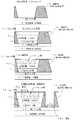
図1(a〜d)は本発明の半導体素子の製造方法の実施形態の一例を示すものである。工程に従って説明する。なお、ここでもPDを作製する場合について説明する。
工程(a)絶縁膜(酸化膜又は窒化膜)形成・パターニング
加熱されたn型Inp基板上1にSiH4とN2Oの混合雰囲気をプラズマ分解することでSi酸化膜を形成し、その酸化膜をフォトリソグラフィによりパターニングし、弗酸などでエッチングして分離すべき素子単位の囲い10を形成する。
1A to 1D show an example of an embodiment of a method for manufacturing a semiconductor device of the present invention. It demonstrates according to a process. Here, a case where a PD is manufactured will be described.
Step (a) Formation / patterning of insulating film (oxide film or nitride film) A Si oxide film is formed on a heated n-
工程(b)エピタキシャル成長
前記囲い(Si酸化膜)10が基板に残った状態でInp基板1を数百℃に加熱する。その後、例えばトリメチルインジウムやトリメチルガリウム、アルシン,ホスフィンを流し、この基板上にn+型Inpエピ層11や光吸収層となるInGaAs層12及びキャップ層としてのInp層13をエピタキシャル成長などにより形成する。
Step (b) Epitaxial Growth The
この場合、InPやInGaAsはSi酸化膜10上には成長しない。即ち、Si酸化膜はInPやInGaAsが成長する温度では非常に安定な結合をしているため結合手を出していない。そのため、これらがSi酸化膜10上には留まらず「表面上を流れて」n型Inp基板が表出しているところに到達し成長する。その結果、Inp基板1上の表面だけに選択的にエピタキシャル膜が成長することになる。
In this case, InP and InGaAs do not grow on the
工程(c)p+型層形成
基板表面に絶縁膜を形成しフォトリソグラフィによりパターニングし、絶縁膜でマスクされ一部だけキャップ層としてのInp層13が表出した基板をジメチルジンクなどの雰囲気中に入れZnなどの拡散を行い受光部としてのp+型層14を形成する。
Step (c) p + type layer formation An insulating film is formed on the surface of the substrate, patterned by photolithography, and the substrate masked by the insulating film and partially exposed to the
工程(d)反射防止膜・電極形成
基板表面を反射防止膜(例えば窒化膜)などで覆い受光部p+型層14の一部にコンタクトホールを形成する。その部分に電極15aを形成し、また基板裏面にも電極15bを形成する。
上述の製造方法によれば、選択エピタキシャルを行うことで工程が大幅に減少すると共に素子間を安定した酸化膜(囲い)10で分離することで素子のリーク電流特性を改善することができる。
Step (d) Antireflection Film / Electrode Formation The substrate surface is covered with an antireflection film (for example, a nitride film) or the like, and a contact hole is formed in a part of the light receiving portion p + type layer 14. An electrode 15a is formed on that portion, and an electrode 15b is also formed on the back surface of the substrate.
According to the manufacturing method described above, the number of steps can be greatly reduced by performing selective epitaxial, and the device can be improved in leakage current characteristics by separating the devices with a stable oxide film (enclosure) 10.
図2(a〜d)は他の実施形態の一例を示すもので、図1とは基板として半絶縁性InP基板16を用い、基板16の表面にn+型InP17をエピタキシャル成長させる点。および電極15cを基板の表面側に設けた点が異なっている。なお、ここでもPDを作製する場合について説明する。 FIG. 2A to FIG. 2D show an example of another embodiment, which is different from FIG. 1 in that a semi-insulating InP substrate 16 is used as a substrate and n + -type InP 17 is epitaxially grown on the surface of the substrate 16. The difference is that the electrode 15c is provided on the surface side of the substrate. Here, a case where a PD is manufactured will be described.
工程(a)絶縁膜(酸化膜又は窒化膜)形成・パターニング
半絶縁性InP基板16の表面にn+型InP17をエピタキシャル成長させ、この基板を加熱してn+型InP17上にSiH4とN2Oの混合雰囲気をプラズマ分解することでSi酸化膜を形成し、その酸化膜をフォトリソグラフィによりパターニングし、弗酸などでエッチングして分離すべき素子単位の囲い(Si酸化膜)10を形成する。
Step (a) Formation / Patterning of Insulating Film (Oxide Film or Nitride Film) An n + type InP 17 is epitaxially grown on the surface of the semi-insulating InP substrate 16, and this substrate is heated to form SiH 4 and N 2 on the n + type InP 17. An Si oxide film is formed by plasma decomposition of the mixed atmosphere of O, the oxide film is patterned by photolithography, and etched with hydrofluoric acid or the like to form an element unit enclosure (Si oxide film) 10 to be separated. .
工程(b)エピタキシャル成長
前記囲い(Si酸化膜)10が基板に残った状態で半絶縁性Inp基板16を数百℃に加熱する。その後、例えばトリメチルインジウムやトリメチルガリウム、アルシン,ホスフィンを流し基板16上のn+型Inpエピ層17上にn+型Inpエピ層11や光吸収層となるInGaAs層12及びキャップ層としてのInp層13をエピタキシャル成長などにより形成する。
Step (b) Epitaxial Growth The semi-insulating Inp substrate 16 is heated to several hundred degrees Celsius with the enclosure (Si oxide film) 10 remaining on the substrate. Then, for example, trimethyl indium and trimethyl gallium, arsine, Inp layer as InGaAs layer 12 and the cap layer serving as the n + -type
工程(c)p+型層形成
基板表面に絶縁膜を形成しフォトリソグラフィによりパターニングし、絶縁膜でマスクされ一部だけキャップ層としてのInp層13が表出した基板をジメチルジンクなどの雰囲気中に入れZnなどの拡散を行い受光部としてのp+型層14を形成する。
Step (c) p + type layer formation An insulating film is formed on the surface of the substrate, patterned by photolithography, and the substrate masked by the insulating film and partially exposed to the
工程(d)反射防止膜・電極形成
基板表面を反射防止膜(例えば窒化膜)などで覆い受光部p+層14の一部および囲い(Si酸化膜)10の一部にコンタクトホールを形成する。その部分に電極15a,15cを形成する。
このような構成によれば半絶縁性基板16の一方の面に電極があるので、半導体素子の組込み時の自由度を向上させることができる。
Step (d) Antireflection film / electrode formation The substrate surface is covered with an antireflection film (for example, a nitride film) or the like, and contact holes are formed in a part of the light receiving portion p + layer 14 and a part of the enclosure (Si oxide film) 10. . Electrodes 15a and 15c are formed in these portions.
According to such a configuration, since there is an electrode on one surface of the semi-insulating substrate 16, the degree of freedom when incorporating the semiconductor element can be improved.
以上の説明は、本発明の説明および例示を目的として特定の好適な実施例を示したに過ぎない。例えば実施例では半導体素子としてPDを作製したが、例えばトランジスタなどであってもよく、要は分離すべき半導体素子が予め作製された囲いの中に半導体層を積層して形成されるものであればよい。 The foregoing description is merely illustrative of certain preferred embodiments for purposes of explanation and illustration of the invention. For example, in the embodiment, a PD is manufactured as a semiconductor element. However, for example, a transistor may be used. In short, a semiconductor element to be separated is formed by stacking semiconductor layers in a prefabricated enclosure. That's fine.
また、実施例では基板としてn型Inp基板や半絶縁性Inp基板を用いたが、例えばSi基板であってもよい。従って本発明は、上記実施例に限定されることなく、その本質から逸脱しない範囲で更に多くの変更、変形を含むものである。 In the embodiment, an n-type Inp substrate or a semi-insulating Inp substrate is used as the substrate. However, for example, a Si substrate may be used. Therefore, the present invention is not limited to the above-described embodiments, and includes many changes and modifications without departing from the essence thereof.
1 n型InP基板
2,11 n型InPエピタキシャル層
3 光吸収層
4 キャップInP層
5 p+層
6 溝
7,15 電極
8,10 絶縁膜(酸化膜又は窒化膜)
9 ポリイミド膜
12 光吸収層(InGaAs)
13 キャップInP層
DESCRIPTION OF SYMBOLS 1 n-
9 Polyimide film 12 Light absorption layer (InGaAs)
13 Cap InP layer
Claims (4)
Priority Applications (1)
| Application Number | Priority Date | Filing Date | Title |
|---|---|---|---|
| JP2007273287A JP2009105105A (en) | 2007-10-22 | 2007-10-22 | Method of manufacturing semiconductor device |
Applications Claiming Priority (1)
| Application Number | Priority Date | Filing Date | Title |
|---|---|---|---|
| JP2007273287A JP2009105105A (en) | 2007-10-22 | 2007-10-22 | Method of manufacturing semiconductor device |
Publications (1)
| Publication Number | Publication Date |
|---|---|
| JP2009105105A true JP2009105105A (en) | 2009-05-14 |
Family
ID=40706527
Family Applications (1)
| Application Number | Title | Priority Date | Filing Date |
|---|---|---|---|
| JP2007273287A Pending JP2009105105A (en) | 2007-10-22 | 2007-10-22 | Method of manufacturing semiconductor device |
Country Status (1)
| Country | Link |
|---|---|
| JP (1) | JP2009105105A (en) |
Cited By (1)
| Publication number | Priority date | Publication date | Assignee | Title |
|---|---|---|---|---|
| WO2018088083A1 (en) * | 2016-11-11 | 2018-05-17 | ソニーセミコンダクタソリューションズ株式会社 | Light-receiving element, method for manufacturing light-receiving element, and electronic device |
-
2007
- 2007-10-22 JP JP2007273287A patent/JP2009105105A/en active Pending
Cited By (2)
| Publication number | Priority date | Publication date | Assignee | Title |
|---|---|---|---|---|
| WO2018088083A1 (en) * | 2016-11-11 | 2018-05-17 | ソニーセミコンダクタソリューションズ株式会社 | Light-receiving element, method for manufacturing light-receiving element, and electronic device |
| US11646341B2 (en) | 2016-11-11 | 2023-05-09 | Sony Semiconductor Solutions Corporation | Light-receiving device, method of manufacturing light-receiving device, and electronic apparatus |
Similar Documents
| Publication | Publication Date | Title |
|---|---|---|
| US20090020768A1 (en) | Buried contact devices for nitride-based films and manufacture thereof | |
| US10586847B2 (en) | Multilayer device | |
| TWI520175B (en) | Methods for fabricating compound semiconductor cyrstal and electronic device, and semiconductor substrate | |
| TWI500079B (en) | Method and structure having monolithic heterogeneous integration of compound semiconductors with elemental semiconductor | |
| WO2014017063A1 (en) | Semiconductor substrate, method for manufacturing semiconductor substrate, and method for manufacturing composite substrate | |
| US20130062696A1 (en) | SOI Semiconductor Structure with a Hybrid of Coplanar Germanium and III-V, and Preparation Method thereof | |
| US9379204B2 (en) | Lattice matched aspect ratio trapping to reduce defects in III-V layer directly grown on silicon | |
| CN105990375A (en) | Optoelectronics and CMOS integration on GOI substrate | |
| US9773670B2 (en) | Method of preparation of III-V compound layer on large area Si insulating substrate | |
| US9455141B2 (en) | Silicon-germanium fin of height above critical thickness | |
| JP2014072217A (en) | Method of manufacturing photosensor, method of manufacturing infrared sensor, photosensor and compound semiconductor substrate | |
| US10366883B2 (en) | Hybrid multilayer device | |
| KR20110002423A (en) | Reduced defect semiconductor-on-insulator hetero-structures | |
| JP2009105105A (en) | Method of manufacturing semiconductor device | |
| JP2016143718A (en) | Method of manufacturing infrared ray sensor | |
| KR20130054010A (en) | Semiconductor device using iii-v group material and method of manufacturing the same | |
| US9985149B2 (en) | Semiconductor device and method of manufacturing the same | |
| JP2020009861A (en) | Infrared detector, infrared detection device, and manufacturing method for infrared detector | |
| JP6572640B2 (en) | Method for fabricating semiconductor light receiving element | |
| JP2008235709A (en) | Semiconductor device | |
| US11004681B2 (en) | Defect-free heterogeneous substrates | |
| JP2011134888A (en) | Method of manufacturing semiconductor laser element | |
| US20190296181A1 (en) | Aluminum gallium arsenide and indium gallium phosphide power converter on silicon | |
| JP2015135877A (en) | Semiconductor substrate, and method of manufacturing semiconductor substrate | |
| JP6048138B2 (en) | Manufacturing method of optical waveguide element |