JP2009104023A - Polarizer and its manufacturing method - Google Patents
Polarizer and its manufacturing method Download PDFInfo
- Publication number
- JP2009104023A JP2009104023A JP2007277254A JP2007277254A JP2009104023A JP 2009104023 A JP2009104023 A JP 2009104023A JP 2007277254 A JP2007277254 A JP 2007277254A JP 2007277254 A JP2007277254 A JP 2007277254A JP 2009104023 A JP2009104023 A JP 2009104023A
- Authority
- JP
- Japan
- Prior art keywords
- film
- light
- polarizer
- absorption
- polarized light
- Prior art date
- Legal status (The legal status is an assumption and is not a legal conclusion. Google has not performed a legal analysis and makes no representation as to the accuracy of the status listed.)
- Withdrawn
Links
Images


Landscapes
- Polarising Elements (AREA)
- Liquid Crystal (AREA)
- Projection Apparatus (AREA)
- Optical Filters (AREA)
Abstract
Description
本発明は、光学薄膜を用いた偏光子およびその製造方法に関する。 The present invention relates to a polarizer using an optical thin film and a method for manufacturing the same.
偏光子は自然光(無偏光)や円偏光などのランダム光から直線偏光を得るための偏光光学素子であり、吸収型偏光子、反射型偏光子、薄膜型偏光子、複屈折型偏光子など、様々な構成の偏光子が実用化されている。これら偏光子は、高解像度スペクトルカメラや蛍光顕微鏡などに用いられる分光フィルタ(液晶フィルタ)、光の偏光情報を得るための各種計測機器および液晶プロジェクタを構成する偏光変換素子などに広く使用されている。
例えば、1枚または複数枚の液晶セルを1対の偏光子で挟んだ液晶パネルを用いた分光装置が提案されている(特許文献1参照)。また、複数の透明基板の間に入射光に対して所定の屈折率を有する光学的に透明な高屈折率層と低屈折率層とから成る基本構造膜の所定繰り返し構造を有する偏光分離膜を配置して成る偏光ビームスプリッタおよびこの偏光ビームスプリッタを備えて自然光を特定の偏光状態に揃える偏光子が提案されている(特許文献2参照)。
A polarizer is a polarizing optical element for obtaining linearly polarized light from random light such as natural light (non-polarized light) and circularly polarized light. Absorbing polarizer, reflective polarizer, thin film polarizer, birefringent polarizer, etc. Various configurations of polarizers have been put into practical use. These polarizers are widely used in spectral filters (liquid crystal filters) used in high-resolution spectral cameras and fluorescent microscopes, various measuring instruments for obtaining polarization information of light, and polarization conversion elements constituting liquid crystal projectors. .
For example, a spectroscopic device using a liquid crystal panel in which one or a plurality of liquid crystal cells are sandwiched between a pair of polarizers has been proposed (see Patent Document 1). A polarization separation film having a predetermined repeating structure of a basic structure film composed of an optically transparent high refractive index layer having a predetermined refractive index with respect to incident light and a low refractive index layer between a plurality of transparent substrates. A polarizing beam splitter that is arranged and a polarizer that includes the polarizing beam splitter and aligns natural light in a specific polarization state have been proposed (see Patent Document 2).
こうした特許文献1および特許文献2などに示される偏光子には、一方の偏光方向の偏光光を吸収することにより偏光方向を決定する吸収型偏光子、あるいは誘電体薄膜の反射率の入射角度依存性による薄膜型偏光子が用いられている。これらの偏光子は、大きい面積のものを得ることは可能であるが、偏光子に入射する入射光の散乱や反射などの迷光による変換効率(透過率または反射率)の損失を招き易い課題を有している。また、量産化が容易で安価な偏光子が求められている。
In the polarizers shown in
本発明は、上述の課題の少なくとも一部を解決するためになされたものであり、以下の形態または適用例として実現することが可能である。 SUMMARY An advantage of some aspects of the invention is to solve at least a part of the problems described above, and the invention can be implemented as the following forms or application examples.
[適用例1]
本適用例に係る偏光子は、入射光を直線偏光光に作り出す偏光子であって、断面形状が直角三角形の二つの透光性基材が互いの斜辺同士で貼り合わされた矩形柱が、前記入射光の入射面に沿って複数並列配置され、前記透光性基材の前記斜辺の界面に前記入射光を、第1の直線偏光光と第2の直線偏光光とに分離する偏光分離膜と、前記並列配置された前記矩形柱の界面に前記偏光分離膜において分離されて入射する前記第1の直線偏光光を吸収する吸収膜と、前記第2の直線偏光光を射出する光射出面と、を備えたことを特徴とする。
[Application Example 1]
The polarizer according to this application example is a polarizer that generates incident light into linearly polarized light, and a rectangular column in which two translucent substrates having a cross-sectional shape of a right triangle are bonded to each other on the oblique sides of each other, A polarization separation film that is arranged in parallel along the incident surface of incident light and separates the incident light into first linearly polarized light and second linearly polarized light at the interface of the oblique side of the translucent substrate. An absorption film that absorbs the first linearly polarized light that is separated and incident on the interface of the rectangular columns arranged in parallel with each other, and a light exit surface that emits the second linearly polarized light And.
これによれば、偏光子が、断面形状が直角三角形の二つの透光性基材が互いの斜辺同士で貼り合わされた矩形柱が、入射光の入射面に沿って複数並列配置され、透光性基材の斜辺界面に入射光を二種類の第1の直線偏光光と第2の直線偏光光とに分離する偏光分離膜と、並列配置された矩形柱の直角界面に偏光分離膜で分離されて入射する第1の直線偏光光を吸収する吸収膜とを備えることにより、吸収膜において、偏光分離膜で分離されて入射する直線偏光光とともに、入射方向(入射角度)が異なって偏光子に入射する入射光の散乱や反射などによる迷光を吸収し、偏光子から一種類の第2の直線偏光光を射出することができる。すなわち、偏光分離特性が向上した分離効率の高い偏光子が得られる。 According to this, a plurality of rectangular pillars in which two light-transmitting substrates having cross-sectional shapes of right-angled triangles are bonded to each other on the oblique sides are arranged in parallel along the incident light incident surface, The separation of the incident light into two kinds of first linearly polarized light and second linearly polarized light at the oblique side interface of the base material, and the polarization separation film at the right angle interface of the rectangular columns arranged in parallel And an absorbing film that absorbs the incident first linearly polarized light, and the incident light (incident angle) is different in the absorbing film together with the linearly polarized light that is separated by the polarization separating film and incident. It is possible to absorb stray light caused by scattering or reflection of incident light incident on the light and to emit one type of second linearly polarized light from the polarizer. That is, a polarizer with high separation efficiency and improved polarization separation characteristics can be obtained.
[適用例2]
上記適用例に係る偏光子において、前記吸収膜は誘電体多層膜より成り、少なくともSi、TiOx、Nb2O5の内のいずれかの誘電体膜より成る吸収層を含むのが好ましい。
これによれば、矩形柱の界面に形成された吸収膜が誘電体多層膜より成り、少なくともSi、TiOx、Nb2O5のうちのいずれかの誘電体膜より成る吸収層を含むことにより、偏光分離膜で分離されて入射する直線偏光光とともに、入射角度が異なって偏光子に入射する入射光の散乱や反射などによる迷光を吸収することができる。
[Application Example 2]
In the polarizer according to the application example described above, it is preferable that the absorption film includes a dielectric multilayer film and includes an absorption layer including at least one of a dielectric film of Si, TiO x , and Nb 2 O 5 .
According to this, the absorption film formed at the interface of the rectangular column is made of a dielectric multilayer film, and includes an absorption layer made of at least one of the dielectric films of Si, TiO x , and Nb 2 O 5. In addition to the linearly polarized light incident after being separated by the polarization separation film, stray light due to scattering or reflection of incident light having different incident angles and incident on the polarizer can be absorbed.
[適用例3]
本適用例に係る偏光子は、前記吸収膜は、前記吸収層と反射防止層とを含み構成されているのが好ましい。
これによれば、矩形柱の界面に形成された吸収膜が吸収層と反射防止層とを含み構成されていることにより、透過率および反射率ともに略0(ゼロ)に近い値の優れた光吸収性能を備えた吸収膜が得られる。したがって、偏光分離膜で分離されて入射する直線偏光光とともに、入射角度が異なって偏光子に入射する入射光の散乱や反射などによる迷光を吸収することができる。
[Application Example 3]
In the polarizer according to this application example, it is preferable that the absorption film includes the absorption layer and an antireflection layer.
According to this, since the absorption film formed at the interface of the rectangular column includes the absorption layer and the antireflection layer, both the transmittance and the reflectance are excellent light with values close to approximately 0 (zero). An absorption film having absorption performance is obtained. Therefore, stray light caused by scattering or reflection of incident light having different incident angles and incident on the polarizer can be absorbed together with linearly polarized light incident after being separated by the polarization separation film.
[適用例4]
本適用例に係る偏光子の製造方法は、透光性基板の一方の表面上に、入射光を二種類の直線偏光光に分離する偏光分離膜を形成する偏光分離膜形成工程と、複数の前記透光性基板の前記偏光分離膜が形成された面を一方方向に揃えて板厚方向に順次重ね合わせて貼り合わせたガラスブロックを形成するガラスブロック形成工程と、前記ガラスブロックを、該ガラスブロックの表面と略45°の角度を成す互いに略平行な複数の切断線に沿って切断して、複数の素子ユニットを形成するガラスブロック切断工程と、複数の前記素子ユニットの一方の表面上に、二種類の前記直線偏光光の一方を吸収する吸収膜を形成する吸収膜形成工程と、複数の前記素子ユニットの前記吸収膜が形成された面を一方方向に揃えて、前記素子ユニットに形成された前記偏光分離膜が略一直線上となるように位置決めして板厚方向に順次重ね合わせて貼り合わせた素子ブロックを形成する素子ブロック形成工程と、前記素子ブロックを、該素子ブロックの表面と略90°の角度を成す互いに略平行な複数の切断線に沿って切断する素子ブロック切断工程と、を備えたことを特徴とする。
[Application Example 4]
A method for manufacturing a polarizer according to this application example includes a polarization separation film forming step of forming a polarization separation film that separates incident light into two types of linearly polarized light on one surface of a light-transmitting substrate, and a plurality of steps A glass block forming step of forming a glass block in which the surface of the translucent substrate on which the polarization separation film is formed is aligned in one direction and is sequentially stacked and bonded together, and the glass block is made of the glass A glass block cutting step of forming a plurality of element units by cutting along a plurality of substantially parallel cutting lines forming an angle of about 45 ° with the surface of the block, and on one surface of the plurality of element units Forming an absorption film that absorbs one of the two types of linearly polarized light, and forming the absorption unit on the element unit by aligning the surface of the element unit on which the absorption film is formed in one direction. Is An element block forming step of forming an element block in which the polarization separation film is positioned so as to be substantially in a straight line and are sequentially stacked and bonded together in the plate thickness direction; And an element block cutting step of cutting along a plurality of cutting lines substantially parallel to each other at an angle of °.
この製造方法によれば、透光性基板の一方の表面上に入射光を二種類の直線偏光光に分離する偏光分離膜を形成する偏光分離膜形成工程と、複数の透光性基板の偏光分離膜が形成された面を一方方向に揃えて板厚方向に順次重ね合わせて貼り合わせるガラスブロック形成工程と、ガラスブロックの表面と略45°の角度を成す互いに略平行な複数の切断線に沿って切断して複数の素子ユニットを形成するガラスブロック切断工程と、複数の素子ユニットの一方の表面上に、二種類の直線偏光光の一方を吸収する吸収膜を形成する吸収膜形成工程と、素子ユニットに形成された偏光分離膜が略一直線上となるように位置決めして板厚方向に順次重ね合わせて貼り合わせる素子ブロック形成工程と、素子ブロックの表面と略90°の角度を成す互いに略平行な複数の切断線に沿って切断する素子ブロック切断工程と、を備えることによって、断面形状が直角三角形の二つの透光性基材の斜辺同士で貼り合わされた矩形柱の斜辺界面に偏光分離膜と、並列配置された矩形柱の直角界面に偏光分離膜において分離されて入射する直線偏光光を吸収する吸収膜が形成された偏光子を、一度に多数を得ることができる。すなわち、量産化が容易で、しかも安価な偏光子を得ることができる。 According to this manufacturing method, a polarization separation film forming step for forming a polarization separation film for separating incident light into two types of linearly polarized light on one surface of the light transmissive substrate, and polarization of a plurality of light transmissive substrates A glass block forming process in which the surface on which the separation film is formed is aligned in one direction and is sequentially stacked and bonded in the thickness direction, and a plurality of cutting lines that are substantially parallel to each other and form an angle of about 45 ° with the surface of the glass block. A glass block cutting step for forming a plurality of element units by cutting along an absorption film forming step for forming an absorption film for absorbing one of two types of linearly polarized light on one surface of the plurality of element units; An element block forming step in which the polarization separation films formed on the element unit are positioned so as to be substantially in a straight line and are sequentially stacked and bonded together in the thickness direction, and the surface of the element block forms an angle of approximately 90 ° with each other. An element block cutting step that cuts along a plurality of cutting lines substantially parallel to the cross-section of the rectangular column bonded to each other between the hypotenuses of two translucent substrates having a right-angled triangular cross-section. It is possible to obtain a large number of polarizers each having a polarization separating film and an absorbing film that absorbs linearly polarized light that is separated and incident on the orthogonal interface between the rectangular columns arranged in parallel. That is, it is possible to obtain a polarizer that is easily mass-produced and that is inexpensive.
また、透光性基板の板厚、透光性基板の平面サイズおよび使用枚数を適宜選択することで、所望の平面サイズ又は/及び厚さの偏光子を容易に得ることができる。したがって、大きな平面サイズの偏光子、あるいは厚さの薄い偏光子が容易に得られ、広い面積を有する測定物の偏光情報を測定する分光器や、各種光学機器における薄型光学フィルタとして広く適用することができる。 Moreover, the polarizer of a desired plane size or / and thickness can be obtained easily by selecting suitably the board | plate thickness of a translucent board | substrate, the planar size of a translucent board | substrate, and the number of sheets to be used. Therefore, a large planar size polarizer or a thin thickness polarizer can be easily obtained, and it can be widely applied as a spectroscope for measuring polarization information of a measurement object having a large area and as a thin optical filter in various optical instruments. Can do.
以下、実施形態を図面に基づいて説明する。
図1(a)は本実施形態に係る偏光子の構成を模式的に示す正面図であり、図1(b)は図1(a)のA−A断面における偏光子を模式的に示す断面図である。なお、これらの図面は、説明の便宜のために各構成要素の寸法や比率を実際のものとは異ならせてある。
Hereinafter, embodiments will be described with reference to the drawings.
Fig.1 (a) is a front view which shows typically the structure of the polarizer which concerns on this embodiment, FIG.1 (b) is a cross section which shows typically the polarizer in the AA cross section of Fig.1 (a). FIG. In these drawings, the dimensions and ratios of each component are different from actual ones for convenience of explanation.
図1(a)および図1(b)において、偏光子1は、断面形状が直角三角形を成して正面図(図1(a))中に示すy方向に延伸する透光性基材としてのガラス材11と、同様に断面形状がガラス材11と同一の直角三角形を成してy方向に延伸する透光性基材としてのガラス材12とが、互いの斜辺で貼り合わされた多数の矩形柱13が、光入射面1aおよび光射出面1bに沿って並列配置され、正面視、矩形形状を成している。
1 (a) and 1 (b), a
ガラス材11とガラス材12とが貼り合わされた直角三角形の斜辺(斜辺界面)には、偏光分離膜14が形成されている。また、ガラス材11とガラス材12とが貼り合わされた矩形柱13がx方向に順次貼り合わされた界面(直角界面)には、吸収膜15が形成されている。なお、光入射面1aと光射出面1bとの間隔、すなわち偏光子1の光入射面1a方向における厚さ寸法は、用いる機器などに対応して任意に設定することができるが、薄型を求める場合には1mm〜5mm程度が好ましい。
A
ガラス材11とガラス材12とが貼り合わされた斜辺界面が光入射面1aおよび光射出面1bと成す角度は、略45°である。したがって、ガラス材11およびガラス材12の断面形状は、それぞれ直角二等辺三角形を成している。すなわち、斜辺界面に偏光分離膜14が形成された矩形柱13は、それぞれ断面形状が略正方形を成した偏光ビームスプリッタとしての機能を有する。
The angle formed by the hypotenuse interface where the
偏光分離膜14を介して互いに隣り合うガラス材11とガラス材12、および光入射面1aおよび光射出面1bに沿う方向に吸収膜15を介して隣り合う矩形柱13同士は、それぞれ接着剤(図示せず)により貼着されて(貼り合わされて)いる。接着剤としては、例えば、接着加工が容易で比較的高温度に耐えうる一液性エポキシまたは一液性アクリル系の紫外線硬化型接着剤を用いることができる。接着剤(接着層)の厚さは、例えば10μm程度である。
なお、これらの貼り合わせには、接着剤に代えて粘着剤を用いたり、シランカップリング剤を塗布する又は/及び活性エネルギー線を照射する直接接合法を用いることができる。
The
In addition, it can replace with an adhesive agent and can use the direct joining method which apply | coats a silane coupling agent and / or irradiates an active energy ray for these bonding.
ガラス材11およびガラス材12の材質は、透光性を有する基材(透光性基材)であれば限定されない。したがって、白板ガラス、各種光学ガラス、ホウケイ酸ガラスおよび青板ガラスなどを用いることができる。本実施形態におけるガラス材11およびガラス材12は、例えば白板ガラスよりなる。
The material of the
偏光分離膜14は、誘電体多層膜で形成される。誘電体多層膜は、例えば、SiO2(二酸化ケイ素)、MgF2(フッ化マグネシウム)、ランタンアルミネートなどより成る低・中屈折率層と、TiO2(二酸化チタン)、Ta2O5(酸化タンタル)などより成る高屈折率層とが、所定の順序および光学膜厚で形成された多層膜が挙げられる。偏光分離膜14は、入射する光線束(s偏光光+p偏光光)を、s偏光の部分光線束(s偏光光)とp偏光の部分光線束(p偏光光)とに分離して、s偏光光を反射し、p偏光光を透過する機能(偏光分離機能)を有する。
The
吸収膜15は、例えば、Ta2O5、SiO2、Al2O3(酸化アルミニウム)、ランタンチタネートなどの誘電体膜より成る反射防止層と、Si(シリコン)、TiOx、Nb2O5(五酸化ニオブ)などの誘電体膜よりなる吸収層とが、所定の順序および光学膜厚で組み合わされた誘電体多層膜で構成される。吸収膜15は、所定の波長領域において透過率および反射率の値が略0(ゼロ)の不透明膜であり、偏光分離膜14において反射されて入射するs偏光光を主体とする偏光光を吸収する光吸収機能を有する。
The
なお、TiOxは、通常のTiO2結晶内のTiが八面体六配位であるのに対して四面体配位で構成され、Ti量によって吸収ベクトルを変位することができる物質である。また、Ta2O5は、成膜条件(光学膜厚)の違いにより吸収層にも透明な誘電体層にもなることができる物質である。
偏光分離膜14および吸収膜15は、各誘電体材料を真空蒸着法、スパッタリング法またはイオンプレーティング法などを用いて成膜し、形成される。
Note that TiO x is a substance that is composed of tetrahedral coordination while Ti in the normal TiO 2 crystal is octahedral hexacoordinate, and whose absorption vector can be displaced by the amount of Ti. Ta 2 O 5 is a substance that can be an absorption layer or a transparent dielectric layer depending on the film formation conditions (optical film thickness).
The
こうした偏光分離膜14および吸収膜15の具体的な膜構成を説明する。
なお、膜構成は、可視光波長領域(420nm〜680nm程度)に対して好適な偏光分離膜14および吸収膜15の場合の一例を示す。
A specific film configuration of the
In addition, a film | membrane structure shows an example in the case of the
「表1」は可視光波長領域の偏光分離機能を有する偏光分離膜の膜構成を示し、「表2」は可視光波長領域の光吸収機能を有する吸収膜の膜構成を示す。なお、偏光分離膜の膜構成は、設計波長760nm、入射角度45°における設計値であり、吸収膜の膜構成は、設計波長865nm、入射角度0°における設計値である。 “Table 1” shows a film configuration of a polarization separation film having a polarization separation function in the visible light wavelength region, and “Table 2” shows a film configuration of an absorption film having a light absorption function in the visible light wavelength region. The film configuration of the polarization separation film is a design value at a design wavelength of 760 nm and an incident angle of 45 °, and the film configuration of the absorption film is a design value at a design wavelength of 865 nm and an incident angle of 0 °.
また、それぞれの表には、各多層膜を構成する層No.に対する膜材料、光学膜厚(nd)、物理膜厚(d(nm))を示す。層No.は、成膜されるガラス材11またはガラス材12の表面側から順に1層、2層、3層…と表す。
In each table, the layer numbers constituting each multilayer film are shown. Film thickness, optical film thickness (nd), and physical film thickness (d (nm)). Layer No. Is expressed as one layer, two layers, three layers, ... in order from the surface side of the

一方、吸収膜15は、「表2」に示すように、Ta2O5(酸化タンタル)を1層目として、2層目にSiO2、以後3層目〜8層目にTa2O5とSiO2が交互に成膜され、9層目にTiOx、そして最上層の10層目にSiO2よりなる10層の誘電体多層膜で構成される。この誘電体多層膜中の9層目のTiOx層において光吸収が行われる。
On the other hand, as shown in “Table 2”, the
このように構成された偏光分離膜14の偏光分離特性および吸収膜15の光吸収特性を図2、図3に示す。
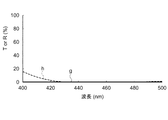
図2は、「表1」に示す(可視光波長領域の偏光分離機能を有する)偏光分離膜の透過率および反射率の波長分散特性を示すグラフであり、図3は、「表1」に示す(可視光波長領域の光吸収機能を有する)吸収膜の透過率および反射率の波長分散特性を示すグラフである。
FIG. 2 and FIG. 3 show the polarization separation characteristics of the
FIG. 2 is a graph showing the wavelength dispersion characteristics of transmittance and reflectance of the polarization separation film (having a polarization separation function in the visible light wavelength region) shown in “Table 1”. FIG. It is a graph which shows the wavelength dispersion characteristic of the transmittance | permeability and reflectance of an absorption film (having the light absorption function of visible light wavelength region) to show.
グラフの横軸は、波長領域400nm〜750nmの範囲における入射光の波長(nm)を示し、縦軸にp偏光光の透過率(T(%))またはs偏光光の反射率(R(%))を示す。なお、各図に示す線図a〜線図dは、計算により求めた波長領域400nm〜750nmにおける1nm毎のプロット点を結んだ線図である。 The horizontal axis of the graph indicates the wavelength (nm) of incident light in the wavelength range of 400 nm to 750 nm, and the vertical axis indicates the transmittance (T (%)) of p-polarized light or the reflectance (R (%) of s-polarized light. )). Each of the diagrams a to d shown in each drawing is a diagram connecting plot points for every 1 nm in the wavelength region of 400 nm to 750 nm obtained by calculation.
図2において、線図aで示す偏光分離膜14の可視光波長領域(420nm〜680nm程度)におけるp偏光光の透過率は、平均値が99.68%、最小値であっても98.76%であり、優れた透過性能を備えている。一方、線図bで示すs偏光光の反射率は、平均値が99.44%、最小値であっても98.95%であり、優れた反射性能を備えている。
In FIG. 2, the transmittance of p-polarized light in the visible light wavelength region (about 420 nm to 680 nm) of the
一方、図3において、線図cで示す吸収膜15の可視光波長領域(420nm〜680nm程度)における透過率の平均値は0.16%、線図dで示す反射率の平均値は0.54%であり、透過率および反射率ともに略0(ゼロ)に近い値を示し、優れた光吸収性能を備えている。
On the other hand, in FIG. 3, the average value of the transmittance in the visible light wavelength region (about 420 nm to 680 nm) of the
次に、このように構成された偏光子1に入射する入射光の動作について説明する。
Next, the operation of the incident light that enters the
図1(b)において、システム光軸ALに沿って偏光子1の光入射面1aに入射した光線束(s偏光光+p偏光光)は、ガラス材11とガラス材12との斜辺界面に形成された偏光分離膜14に、略45°の入射角で入射して、第1の直線偏光光としてのs偏光光と、第2の直線偏光光としてのp偏光光との2つの部分光線束に分離される。そして、偏光分離膜14において分離されたp偏光光は偏光分離膜14を透過して光射出面1b側に向かう。一方、偏光分離膜14において分離されたs偏光光は、偏光分離膜14で反射されて直角界面に形成された吸収膜15に向かい、吸収膜15に対して略0°の入射角で入射して、吸収膜15に吸収される。すなわち、偏光子1の光入射面1aに入射した光(s偏光光+p偏光光)は、一種類のp偏光光(直線偏光光)のみが、光射出面1bからシステム光軸ALに略平行方向に射出される。
In FIG. 1B, the light bundle (s-polarized light + p-polarized light) incident on the
なお、吸収膜15では、偏光分離膜14において透過されずに反射された一部のp偏光光や、光入射面1aより入射してガラス材11とガラス材12内に散乱した迷光なども吸収される。さらに、吸収膜15において吸収されずに吸収膜15を透過した些細な量の一部の偏光光の内のs偏光光は、隣り合うガラス材11とガラス材12との斜辺界面に形成された偏光分離膜14に入射した後に、偏光分離膜14において反射されて光入射面1a側に向かい、光入射面1aから射出される。
The
一方、p偏光光は、隣り合うガラス材11とガラス材12との斜辺界面に形成された偏光分離膜14に入射した後に、偏光分離膜14を透過して、隣り合う直角界面に形成された吸収膜15に向かい、その吸収膜15に吸収される。したがって、偏光分離特性が向上し、変換効率の高い偏光子1が得られる。
On the other hand, the p-polarized light is incident on the
次に、このように構成された偏光子1の製造方法について説明する。
図4および図5は、本実施形態に係る偏光子を製造する主要な工程を示す工程断面図である。なお、これらの図面は、説明の便宜のために各構成要素の寸法や比率を実際のものとは異ならせてある。
Next, a manufacturing method of the
4 and 5 are process cross-sectional views showing main processes for manufacturing the polarizer according to the present embodiment. In these drawings, the dimensions and ratios of each component are different from actual ones for convenience of explanation.
先ず、図4(a)に示す工程では、同一の矩形状の外形形状で同一の所定厚さの白板ガラスより成る複数の透光性基板としてのガラス板111を準備して、それぞれのガラス板111の2つの表面のうちの一方の表面上に、偏光分離膜14を形成する(偏光分離膜形成工程)。なお、本実施形態におけるガラス板111の所定厚さは、例えば3mm程度である。
First, in the process shown in FIG. 4A, a plurality of
偏光分離膜14は、上記「表1」に示したSiO2を1層目として、2層目にランタンアルミネート、以後3層目〜36層目に、MgF2とランタンアルミネートとが交互に成膜されて、最上層をSiO2とする37層の誘電体多層膜が形成される。偏光分離膜14は、各誘電体材料を真空蒸着法、スパッタリング法またはイオンプレーティング法などを用いて成膜される。
The
このガラス板111は、後に断面形状が直角三角形を成した柱状のガラス材11およびガラス材12(矩形柱13)を形成する。
なお、図4(a)および図5を含む以後の図面において、ガラス板111は、実際の枚数とは異なる省略した枚数で示す。
This
In the subsequent drawings including FIG. 4A and FIG. 5, the
そして、図4(b)に示す工程では、偏光分離膜形成工程において偏光分離膜14が形成された複数のガラス板111を、それぞれのガラス板111の偏光分離膜14が形成された面を一方方向に揃えて板厚方向に順次重ね合わせて、それぞれの界面に紫外線硬化型接着剤(図示せず)を塗布してガラス板111同士を互いに貼り合わせる(ガラスブロック形成工程)。
界面に塗布された紫外線硬化型接着剤は、ケミカルランプや高圧水銀灯などの光(紫外線)を照射することによって硬化される。これにより複数のガラス板111同士が板厚方向に重ね合わされて、重なり合う界面に偏光分離膜14が配置されたガラスブロック112が形成される。
4B, the plurality of
The ultraviolet curable adhesive applied to the interface is cured by irradiating light (ultraviolet light) such as a chemical lamp or a high pressure mercury lamp. As a result, a plurality of
そして、図4(c)に示す工程では、ガラスブロック形成工程において形成されたガラスブロック112を、互いに略平行な複数の切断線CL1(図中、一点鎖線で示す)に沿って切断する(ガラスブロック切断工程)。
切断線CL1が、ガラス板111の表面と成す角度αは、略45°であり、切断線CL1同士のガラス板111の表面における間隔は、後に光入射面1aを構成するガラス板111の断面形状における直角三角形の辺の長さである。
切断線CL1に沿って切断されたガラスブロック112からは、図中にドットで示す領域形状の素子ユニット113が複数切り出される。
In the step shown in FIG. 4C, the
The angle α that the cutting line CL1 forms with the surface of the
From the
そして、工程として図示しないが、ガラスブロック切断工程において切り出された素子ユニット113の2つの表面のうちの一方の表面上に、吸収膜15を形成する(吸収膜形成工程)。素子ユニット113の表面に形成される吸収膜15は、上記「表2」に示したTa2O5を1層目として、2層目にSiO2、3層目にTa2O5、4層目にSiO2、5層目にTa2O5、6層目にSiO2、7層目にTa2O5、8層目にSiO2、9層目にTiOx、最上層の10層目にSiO2よりなる、10層の誘電体多層膜SiO2が形成される。吸収膜15は、各誘電体材料を真空蒸着法、スパッタリング法またはイオンプレーティング法などを用いて成膜される。
そして、図5(a)に示す工程では、一方の表面上に吸収膜15が形成された複数の素子ユニット113を準備する(素子ユニット準備工程)。
And although not shown as a process, the
5A, a plurality of
そして、図5(b)に示す工程では、素子ユニット準備工程において準備された複数の素子ユニット113を、それぞれの素子ユニット113の吸収膜15が形成された面を一方方向に揃えて板厚方向に順次重ね合わせて、それぞれの界面に紫外線硬化型接着剤(図示せず)を塗布して素子ユニット113同士を互いに貼り合わせる(素子ブロック形成工程)。
素子ユニット113同士の貼り合わせの際には、それぞれの素子ユニット113に形成された複数の偏光分離膜14が略一直線上となるように位置決めして重ね合わされる。
In the step shown in FIG. 5B, the plurality of
When the
界面に塗布された紫外線硬化型接着剤は、ケミカルランプや高圧水銀灯などの光(紫外線)を照射することによって硬化される。これにより複数の素子ユニット113同士が板厚方向に重ね合わされて、重なり合う界面に吸収膜15が配置された素子ブロック114が形成される。
The ultraviolet curable adhesive applied to the interface is cured by irradiating light (ultraviolet light) such as a chemical lamp or a high pressure mercury lamp. Thereby, a plurality of
そして、図5(c)に示す工程では、素子ブロック形成工程において形成された素子ブロック114を、互いに略平行な複数の切断線CL2(図中、一点鎖線で示す)に沿って切断する(素子ブロック切断工程)。
素子ブロック114を切断する切断線CL2は、素子ブロック114を形成する最上段に位置する素子ユニット113に形成された偏光分離膜14の表面位置毎に、素子ブロック114の表面と成す角度βが略90°に切断される。切断線CL2に沿って切断された素子ブロック114からは、図中にドットで示す領域形状の偏光子1が複数切り出されて、偏光子1が完成する。切断線CL2に沿って切断されて切り出された偏光子1の切断面方向における厚さは、3mm程度である。
In the step shown in FIG. 5C, the
The cutting line CL2 that cuts the
完成した偏光子1は、互いに断面形状が直角三角形を成したガラス材11とガラス材12とが貼り合わされた斜辺界面に偏光分離膜14と、ガラス材11とガラス材12とが貼り合わされた矩形柱13が順次貼り合わされた直角界面に吸収膜15とを備え、光入射面1aに入射する光線束(s偏光光+p偏光光)の内のp偏光光(直線偏光光)のみを、光射出面1bからシステム光軸ALに略平行方向に射出する機能を有する(図1参照)。
The completed
なお、偏光子1の製造方法は主要な工程のみ説明したが、ガラスブロック切断工程および素子ブロック切断工程の後には、各ブロックが切断されて形成された素子ユニット113および偏光子1のそれぞれの切断面を、片面ポリッシュ装置または両面ポリッシュ装置を用いて研磨することで、切断面の平坦度および面精度を整えるのが好ましい。
In addition, although the manufacturing method of the
また、完成した偏光子1には、少なくとも一方の面または双方の面に、反射防止(AR)層を設けてもよい。偏光子1は、構成要素が全て無機物で構成されて耐光性、耐熱性に優れることから、AR膜の形成の際に高温に加熱処理することが可能となり、例えば、二酸化珪素、酸化チタンなどの物質を蒸着またはスパッタリング処理した広帯域AR膜を形成することができる。
Further, the completed
さらに、上記偏光子1の製造方法は、素子ブロック114が複数の切断線CL2に沿って切断することにより、図1に示す偏光子1が完成する場合で説明したが、準備するガラス板111の平面サイズや枚数は、所望とする偏光子のサイズに対応して適宜設定することができる。したがって、この場合には、素子ブロック114を複数の切断線CL2に沿って切断した後に、所定サイズや所定の外形形状に、切断および切断面の研磨などを行うのが好ましい。
Furthermore, although the manufacturing method of the
さらにまた、偏光子1は、次のように構成することもできる。
図5(b)に示す素子ブロック形成工程において、紫外線硬化型接着剤に代えて粘着剤などを用いて、素子ユニット113同士を仮接着した素子ブロック114を形成する。そして、その素子ブロック114を図5(c)に示す素子ブロック切断工程において互いに略平行な複数の切断線CL2に沿って切断した後に、切断された偏光子1から仮接着した粘着剤層を剥がして、斜辺界面に偏光分離膜14を有し、直角界面の一方の面に吸収膜15が形成された複数の矩形柱13に分離する。そして、所定個数の矩形柱13を、形成された吸収膜15方向を揃えて並列配置した後、外周部をホルダなどで一体に固定して所望平面サイズの偏光子1が完成する。この構成によれば、サイズの異なるホルダに所定数の矩形柱13を並列配置することで、平面サイズの異なる偏光子1を容易に得ることができる。
Furthermore, the
In the element block forming step shown in FIG. 5B, an
このように構成および製造された偏光子1は、偏光子1の配置方向を替えることによって、入射する非偏光光に対してp波またはs波の偏光光を射出する機能を得ることができる。
図14(a)は完成した偏光子の正面、上面および側面を一括して示す模式図であり、図14(b)は同図(a)に示す偏光子の正面図に対して90°の角度回転した状態の正面、上面および側面を一括して示す模式図である。
The
FIG. 14 (a) is a schematic view showing the front, top and side surfaces of the completed polarizer in a lump, and FIG. 14 (b) is 90 ° with respect to the front view of the polarizer shown in FIG. 14 (a). It is a schematic diagram which shows the front surface, the upper surface, and the side surface of the state which rotated the angle collectively.
上記において説明したように、図14(a)において、偏光子1を柱状の各ガラス材11,12が延伸する方向をy軸方向に配置して用いることによって、システム光軸に略平行に光入射面1aに入射する非偏光光を、電界が光入射面1aに対して水平方向のp波(TM波)の偏光光を射出することができる。
As described above, in FIG. 14 (a), the
一方、その偏光子1を90°の角度、右回転して、図14(b)に示すように、偏光子1を構成する柱状の各ガラス材11,12が延伸する方向をx軸方向に配置して用いることによって、システム光軸に略平行に光入射面1aに入射する非偏光光を、電界が光入射面1aに対して垂直方向のs波(TE波)の偏光光を射出することができる。
なお、偏光子1の回転方向は、右回転または左回転のどちらであってもよい。
On the other hand, the
The rotation direction of the
以上に説明した偏光子1は、入射する光(s偏光光+p偏光光)から一種類のp偏光光またはs偏光光の内のどちらか一種類の直線偏光光を射出する光学素子として、透過型プロジェクタ、反射型プロジェクタなどの照明光学系に好ましく用いることができる。こうしたプロジェクタにおいては、特に、波長が短くパワーの強い青色光の射出側用の偏光子として用いることにより、耐光性をより向上することができる。
The
また、偏光子1は、断面形状が直角二等辺三角形のガラス材11およびガラス材12が互いの斜辺で貼り合わされた複数の矩形柱13が、光入射面1aに沿って並列配置されて製造されるので、大きいサイズ(広い面積)で、しかも薄型の偏光子1を容易に得ることが可能である。これにより、広い面積を有する測定物の偏光情報を測定する分光器や、各種光学機器における光学フィルタなどとして好適に用いることができる。
Further, the
以上のように、本実施形態の偏光子1は、断面形状が直角三角形の二つのガラス材11,12が互いの斜辺同士で貼り合わされた矩形柱13が、光入射面1aに沿って複数並列配置され、ガラス材11,12の斜辺界面に入射光を二種類の直線偏光光に分離する偏光分離膜14と、並列配置された矩形柱13の直角界面に偏光分離膜14において分離されて入射する直線偏光光を吸収する吸収膜15とを備えることにより、吸収膜15において偏光分離膜14で分離されて入射する直線偏光光とともに、入射方向(入射角度)が異なって偏光子1に入射する入射光の散乱や反射などによる迷光を吸収し、偏光子1から一種類の直線偏光光(p偏光光)を射出することができる。すなわち、入射する自然光(無偏光)や円偏光などのランダム光の可視光波長領域にわたり偏光分離特性の向上した分離効率の高い偏光子1が得られる。
As described above, in the
また、吸収膜15が、少なくともSi、TiOx、Nb2O5のうちのいずれかの誘電体膜より成る吸収層を含む誘電体多層膜より成ることにより、偏光分離膜14で分離されて入射するs偏光光とともに、入射角度が異なって偏光子1に入射する入射光の散乱や反射などによる迷光を吸収することができる。また、吸収膜15が吸収層と反射防止層とを含み構成されていることにより、透過率および反射率ともに略0(ゼロ)に近い値の優れた光吸収性能を備えた吸収膜15が得られる。
Further, the
また、偏光子1の製造方法が、ガラス板111の一方の表面上に偏光分離膜14を形成する偏光分離膜形成工程と、複数のガラス板111の偏光分離膜14が形成された面を一方方向に揃えて板厚方向に順次重ね合わせて貼り合わせるガラスブロック形成工程と、ガラスブロック112の表面と略45°の角度を成す互いに略平行な複数の切断線CL1に沿って切断して複数の素子ユニット113を形成するガラスブロック切断工程と、複数の素子ユニット113の一方の表面上に吸収膜15を形成する吸収膜形成工程と、素子ユニット113に形成された偏光分離膜14が略一直線上となるように位置決めして板厚方向に順次重ね合わせて貼り合わせる素子ブロック形成工程と、素子ブロック114の表面と略90°の角度を成す互いに略平行な複数の切断線CL2に沿って切断する素子ブロック切断工程と、を備えることによって、断面形状が直角三角形の二つのガラス材11,12の斜辺同士で貼り合わされた矩形柱13の斜辺界面に偏光分離膜14と、並列配置された矩形柱13の直角界面に吸収膜15が形成された偏光子1を、一度に多数得ることができる。すなわち、量産化が容易で、しかも安価な偏光子1を得ることができる。さらに、偏光子1の製造方法は、ガラス材11,12の板厚、ガラス材11,12の平面サイズおよび使用枚数を適宜選択することで、所望の平面サイズ又は/及び厚さの偏光子1を容易に得ることができる。したがって、大きな平面サイズの偏光子1、あるいは厚さの薄い偏光子1が容易に得られ、広い面積を有する測定物の偏光情報を測定する分光器や、各種光学機器における薄型光学フィルタとして広く適用することができる。
Further, the manufacturing method of the
なお、以上の本実施形態において、以下の変形例として挙げられているような形態であっても、本実施形態と同様な効果を得ることが可能である。 It should be noted that, in the above-described embodiment, even if the form is exemplified as the following modification, it is possible to obtain the same effect as the present embodiment.
(変形例1)
上記実施形態において、偏光子1に形成された偏光分離膜14および吸収膜15が、可視光波長領域の偏光分離機能および光吸収機能を有する場合で説明したが、可視光波長領域に代えて青色光波長域、緑色光波長域または赤色光波長域に略対応した膜構成とすることができる。こうした各色光波長域に対応した偏光分離膜14および吸収膜15を備えた偏光子1は、例えば、透過型プロジェクタなどにおいて、各色光間のクロストークを防止したり、コントラストを高めるなどを目的に、各色光用LCDの光射出側に配置して用いることができる。
(Modification 1)
In the above embodiment, the
「表3」は青色光波長域の偏光分離機能を有する偏光分離膜の膜構成を示し、「表4」は青色光波長域の光吸収機能を有する吸収膜の膜構成を示す。なお、偏光分離膜14の膜構成は、設計波長485nm、入射角度45°における設計値であり、吸収膜15の膜構成は、設計波長485nm、入射角度0°における設計値である。
“Table 3” shows the film configuration of the polarization separation film having the polarization separation function in the blue light wavelength region, and “Table 4” shows the film configuration of the absorption film having the light absorption function in the blue light wavelength region. The film configuration of the
また、それぞれの表には、各多層膜を構成する層No.に対する膜材料、光学膜厚(nd)、物理膜厚(d(nm))を示す。層No.は、成膜されるガラス材11またはガラス材12の表面側から順に1層、2層、3層…と表す。これについては、以後に示す「表5」〜「表10」についても同様である。
In each table, the layer numbers constituting each multilayer film are shown. Film thickness, optical film thickness (nd), and physical film thickness (d (nm)). Layer No. Is expressed as one layer, two layers, three layers, ... in order from the surface side of the
一方、吸収膜15は、「表4」に示すように、Ta2O5(酸化タンタル)を1層目として、2層目にSiO2、3層目にTa2O5、4層目にSiO2、5層目にTiOx、そして最上層の6層目にSiO2よりなる、6層の誘電体多層膜で構成される。この誘電体多層膜中の5層目のTiOx層において光吸収が行われる。
On the other hand, as shown in “Table 4”, the
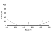
このように構成された偏光分離膜14の偏光分離特性および吸収膜15の光吸収特性を図6、図7に示す。
図6は、「表3」に示す青色光波長域の偏光分離機能を有する偏光分離膜14の透過率および反射率の波長分散特性を示すグラフであり、図7は、「表4」に示す青色光波長域の光吸収機能を有する吸収膜15の透過率および反射率の波長分散特性を示すグラフである。
FIG. 6 and FIG. 7 show the polarization separation characteristics of the
FIG. 6 is a graph showing the wavelength dispersion characteristics of transmittance and reflectance of the
グラフの横軸は、波長領域400nm〜500nmの範囲における入射光の波長(nm)を示し、縦軸にp偏光光の透過率(T(%))またはs偏光光の反射率(R(%))を示す。なお、各図に示す線図e〜線図hは、計算により求めた波長領域400nm〜500nmにおける1nm毎のプロット点を結んだ線図である。
The horizontal axis of the graph indicates the wavelength (nm) of incident light in the wavelength region of 400 nm to 500 nm, and the vertical axis indicates the transmittance (T (%)) of p-polarized light or the reflectance (R (%) of s-polarized light. )). Each of the diagrams e to h shown in each drawing is a diagram connecting plot points for every 1 nm in the
図6において、線図eで示す偏光分離膜14におけるp偏光光の透過率、および線図fで示すs偏光光の反射率は、青色光波長域の429nm〜466nmにおいて、いずれも99%以上の値を示し、青色光波長域における優れた透過性能および反射性能を備えている。
一方、図7において、線図gで示す吸収膜15の透過率および線図hで示す反射率は、偏光分離膜14に対応した青色光波長域の429nm〜466nmにおいて、共に0.5%以下の値を示し、青色光波長域における優れた光吸収性能を備えている。
In FIG. 6, the transmittance of p-polarized light in the
On the other hand, in FIG. 7, the transmittance of the
「表5」は緑色光波長域の偏光分離機能を有する偏光分離膜の膜構成を示し、「表6」は緑色光波長域の光吸収機能を有する吸収膜の膜構成を示す。なお、偏光分離膜14の膜構成は、設計波長550nm、入射角度45°における設計値であり、吸収膜15の膜構成は、設計波長555nm、入射角度0°における設計値である。
“Table 5” shows the film configuration of the polarization separation film having the polarization separation function in the green light wavelength region, and “Table 6” shows the film configuration of the absorption film having the light absorption function in the green light wavelength region. The film configuration of the
一方、吸収膜15は、「表6」に示すように、Ta2O5(酸化タンタル)を1層目として、2層目にSiO2、3層目にTa2O5、4層目にSiO2、5層目にTiOx、そして最上層の6層目にSiO2よりなる、6層の誘電体多層膜で構成される。この誘電体多層膜中の5層目のTiOx層において光吸収が行われる。
On the other hand, as shown in “Table 6”, the
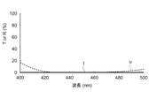
このように構成された偏光分離膜14の偏光分離特性および吸収膜15の光吸収特性を図8、図9に示す。
図8は、「表5」に示す緑色光波長域の偏光分離機能を有する偏光分離膜14の透過率および反射率の波長分散特性を示すグラフであり、図9は、「表6」に示す緑色光波長域の光吸収機能を有する吸収膜15の透過率および反射率の波長分散特性を示すグラフである。
FIG. 8 and FIG. 9 show the polarization separation characteristics of the
FIG. 8 is a graph showing the wavelength dispersion characteristics of transmittance and reflectance of the
グラフの横軸は、波長領域450nm〜600nmの範囲における入射光の波長(nm)を示し、縦軸にp偏光光の透過率(T(%))またはs偏光光の反射率(R(%))を示す。なお、各図に示す線図i〜線図lは、計算により求めた波長領域450nm〜600nmにおける1nm毎のプロット点を結んだ線図である。 The horizontal axis of the graph indicates the wavelength (nm) of incident light in the wavelength region of 450 nm to 600 nm, and the vertical axis indicates the transmittance (T (%)) of p-polarized light or the reflectance (R (%) of s-polarized light. )). Each of the diagrams i to l shown in each figure is a diagram connecting plot points for every 1 nm in a wavelength region of 450 nm to 600 nm obtained by calculation.
図8において、線図iで示す偏光分離膜14におけるp偏光光の透過率、および線図jで示すs偏光光の反射率は、緑色光波長域の526nm〜560nmにおいて、いずれも99%以上の値を示し、緑色光波長域における優れた透過性能および反射性能を備えている。
一方、図9において、線図kで示す吸収膜15の透過率および線図lで示す反射率は、偏光分離膜14に対応した緑色光波長域の526nm〜560nmにおいて、共に0.2%以下の値を示し、緑色光波長域における優れた光吸収性能を備えている。
In FIG. 8, the transmittance of p-polarized light in the
On the other hand, in FIG. 9, the transmittance of the
「表7」は赤色光波長域の偏光分離機能を有する偏光分離膜の膜構成を示し、「表8」は赤色光波長域の光吸収機能を有する吸収膜の膜構成を示す。なお、偏光分離膜14の膜構成は、設計波長670nm、入射角度45°における設計値であり、吸収膜15の膜構成は、設計波長670nm、入射角度0°における設計値である。
“Table 7” shows the film configuration of the polarization separation film having the polarization separation function in the red light wavelength region, and “Table 8” shows the film configuration of the absorption film having the light absorption function in the red light wavelength region. The film configuration of the
一方、吸収膜15は、「表8」に示すように、Ta2O5(酸化タンタル)を1層目として、2層目にSiO2、3層目にTa2O5、4層目にSiO2、5層目にTiOx、そして最上層の6層目にSiO2よりなる、6層の誘電体多層膜で構成される。この誘電体多層膜中の5層目のTiOx層において光吸収が行われる。
On the other hand, as shown in “Table 8”, the
このように構成された偏光分離膜14の偏光分離特性および吸収膜15の光吸収特性を図10、図11に示す。
図10は、「表7」に示す赤色光波長域の偏光分離機能を有する偏光分離膜14の透過率および反射率の波長分散特性を示すグラフであり、図11は、「表8」に示す赤色光波長域の光吸収機能を有する吸収膜15の透過率および反射率の波長分散特性を示すグラフである。
10 and 11 show the polarization separation characteristics of the
FIG. 10 is a graph showing the wavelength dispersion characteristics of transmittance and reflectance of the
グラフの横軸は、波長領域550nm〜750nmの範囲における入射光の波長(nm)を示し、縦軸にp偏光光の透過率(T(%))またはs偏光光の反射率(R(%))を示す。なお、各図に示す線図m〜線図qは、計算により求めた波長領域550nm〜750nmにおける1nm毎のプロット点を結んだ線図である。
The horizontal axis of the graph indicates the wavelength (nm) of incident light in the wavelength region of 550 nm to 750 nm, and the vertical axis indicates the transmittance (T (%)) of p-polarized light or the reflectance (R (%) of s-polarized light. )). Each of the diagrams m to q shown in each figure is a diagram that connects plot points for every 1 nm in the
図10において、線図mで示す偏光分離膜14におけるp偏光光の透過率、および線図nで示すs偏光光の反射率は、赤色光波長域の610nm〜673nmにおいて、いずれも99%以上の値を示し、赤色光波長域における優れた透過性能および反射性能を備えている。
一方、図11において、線図pで示す吸収膜15の透過率および線図qで示す反射率は、偏光分離膜14に対応した赤色光波長域の610nm〜673nmにおいて、共に0.4%以下の値を示し、赤色光波長域における優れた光吸収性能を備えている。
In FIG. 10, the transmittance of p-polarized light in the
On the other hand, in FIG. 11, the transmittance of the
(変形例2)
上記実施形態および変形例1において、偏光子1に形成された吸収膜15が、いずれもTa2O5、SiO2、TiOxの物質よりなる、6層の誘電体多層膜で構成された場合で説明したが、その他にSi(シリコン)、Al2O3(酸化アルミニウム)、Nb2O5(五酸化ニオブ)、LaTiO3(ランタンチタネート)などの物質を用いて構成することができる。
(Modification 2)
In the above-described embodiment and
吸収膜15の他の膜構成例を、前記「変形例1」中に示した青色光波長域の光吸収機能を有する吸収膜を例に説明する。
「表9」は、青色光波長域の光吸収機能を有する吸収膜の別の膜構成を示し、「表10」は、青色光波長域の光吸収機能を有する吸収膜の、さらに別の膜構成を示す。なお、吸収膜15の膜構成は、設計波長485nm、入射角度0°における設計値である。
Another film configuration example of the
“Table 9” shows another film configuration of the absorption film having the light absorption function in the blue light wavelength region, and “Table 10” shows still another film of the absorption film having the light absorption function in the blue light wavelength region. The configuration is shown. The film configuration of the
「表10」に示す吸収膜15は、Nb2O5(五酸化ニオブ)を1層目として、2層目にSiO2、3層目にNb2O5、4層目にSiO2、5層目にTiOx、そして最上層の6層目にSiO2よりなる、6層の誘電体多層膜で構成される。この誘電体多層膜中の5層目のTiOx層において光吸収が行われる。
Absorbing
このように構成された吸収膜15の光吸収特性を図12、図13に示す。
図12は、「表9」に示す青色光波長域の光吸収機能を有する別の吸収膜15の透過率および反射率の波長分散特性を示すグラフであり、図13は、「表10」に示す青色光波長域の光吸収機能を有する、さらに別の吸収膜15の透過率および反射率の波長分散特性を示すグラフである。
The light absorption characteristics of the
FIG. 12 is a graph showing the wavelength dispersion characteristics of the transmittance and reflectance of another
各グラフの横軸は、波長領域400nm〜500nmの範囲における入射光の波長(nm)を示し、縦軸にp偏光光の透過率(T(%))またはs偏光光の反射率(R(%))を示す。なお、各図に示す線図r〜線図uは、計算により求めた波長領域400nm〜500nmにおける1nm毎のプロット点を結んだ線図である。
The horizontal axis of each graph indicates the wavelength (nm) of incident light in the wavelength region of 400 nm to 500 nm, and the vertical axis indicates the transmittance of p-polarized light (T (%)) or the reflectance of s-polarized light (R ( %)). Each of the diagrams r to u shown in each drawing is a diagram connecting plot points for every 1 nm in the
図12において、線図rで示す吸収膜15の透過率、線図sで示す吸収膜15の反射率は、偏光分離膜14に対応した青色光波長域の429nm〜466nmにおいて、0.9%以下の値を示す。また、図13において、線図tで示す透過率、線図uで示す反射率は、0.4%以下の値を示し、共に青色光波長域における優れた光吸収性能を備えている。
なお、以上の変形例2において、吸収膜15の吸収層がTiOxおよびSiより成る場合を例示したが、Nb2O5(五酸化ニオブ)やTa2O5(酸化タンタル)を吸収層とした誘電体多層膜で吸収膜15を構成することもできる。但し、Ta2O5を用いる場合には、光吸収性能が低いために、膜厚の厚い誘電体膜を形成する必要がある。
In FIG. 12, the transmittance of the
In the second modification, the case where the absorption layer of the
1…偏光子、1a…光入射面、1b…光射出面、11,12…透光性基材としてのガラス材、13…矩形柱、14…偏光分離膜、15…吸収膜、111…透光性基板としてのガラス板、112…ガラスブロック、113…素子ユニット、114…素子ブロック。
DESCRIPTION OF
Claims (4)
断面形状が直角三角形の二つの透光性基材が互いの斜辺同士で貼り合わされた矩形柱が、前記入射光の入射面に沿って複数並列配置され、
前記透光性基材の前記斜辺の界面に前記入射光を、第1の直線偏光光と第2の直線偏光光とに分離する偏光分離膜と、
前記並列配置された前記矩形柱の界面に前記偏光分離膜において分離されて入射する前記第1の直線偏光光を吸収する吸収膜と、前記第2の直線偏光光を射出する光射出面と、
を備えたことを特徴とする偏光子。 A polarizer that creates incident light into linearly polarized light,
A plurality of rectangular pillars in which two translucent substrates having a right-angled cross-sectional shape are bonded to each other at the oblique sides are arranged in parallel along the incident surface of the incident light,
A polarization separation film that separates the incident light into the first linearly polarized light and the second linearly polarized light at the oblique side interface of the translucent substrate;
An absorbing film that absorbs the first linearly polarized light that is separated and incident on the interface of the rectangular columns arranged in parallel, and a light exit surface that emits the second linearly polarized light;
A polarizer characterized by comprising:
前記吸収膜は誘電体多層膜より成り、少なくともSi、TiOx、Nb2O5の内のいずれかの誘電体膜より成る吸収層を含むことを特徴とする偏光子。 The polarizer according to claim 1,
The polarizer is characterized in that the absorption film is made of a dielectric multilayer film and includes an absorption layer made of at least one of a dielectric film of Si, TiO x , and Nb 2 O 5 .
前記吸収膜は、前記吸収層と反射防止層とを含み構成されていることを特徴とする偏光子。 The polarizer according to claim 1 or 2, wherein
The polarizer according to claim 1, wherein the absorption film includes the absorption layer and an antireflection layer.
複数の前記透光性基板の前記偏光分離膜が形成された面を一方方向に揃えて板厚方向に順次重ね合わせて貼り合わせたガラスブロックを形成するガラスブロック形成工程と、
前記ガラスブロックを、該ガラスブロックの表面と略45°の角度を成す互いに略平行な複数の切断線に沿って切断して、複数の素子ユニットを形成するガラスブロック切断工程と、
複数の前記素子ユニットの一方の表面上に、二種類の前記直線偏光光の一方を吸収する吸収膜を形成する吸収膜形成工程と、
複数の前記素子ユニットの前記吸収膜が形成された面を一方方向に揃えて、前記素子ユニットに形成された前記偏光分離膜が略一直線上となるように位置決めして板厚方向に順次重ね合わせて貼り合わせた素子ブロックを形成する素子ブロック形成工程と、
前記素子ブロックを、該素子ブロックの表面と略90°の角度を成す互いに略平行な複数の切断線に沿って切断する素子ブロック切断工程と、
を備えたことを特徴とする偏光子の製造方法。 A polarization separation film forming step of forming a polarization separation film that separates incident light into two types of linearly polarized light on one surface of the translucent substrate;
A glass block forming step of forming a glass block in which the surfaces on which the polarization separation films of the plurality of translucent substrates are formed are aligned in one direction and are sequentially stacked and bonded together;
Cutting the glass block along a plurality of cutting lines substantially parallel to each other at an angle of about 45 ° with the surface of the glass block to form a plurality of element units; and
An absorption film forming step of forming an absorption film that absorbs one of the two types of linearly polarized light on one surface of the plurality of element units;
The surfaces of the plurality of element units on which the absorption films are formed are aligned in one direction, and the polarization separation films formed on the element units are positioned so as to be substantially in a straight line, and are sequentially superimposed in the plate thickness direction. An element block forming step for forming an element block bonded together;
An element block cutting step for cutting the element block along a plurality of cutting lines substantially parallel to each other and forming an angle of about 90 ° with the surface of the element block;
A method for producing a polarizer, comprising:
Priority Applications (1)
| Application Number | Priority Date | Filing Date | Title |
|---|---|---|---|
| JP2007277254A JP2009104023A (en) | 2007-10-25 | 2007-10-25 | Polarizer and its manufacturing method |
Applications Claiming Priority (1)
| Application Number | Priority Date | Filing Date | Title |
|---|---|---|---|
| JP2007277254A JP2009104023A (en) | 2007-10-25 | 2007-10-25 | Polarizer and its manufacturing method |
Publications (2)
| Publication Number | Publication Date |
|---|---|
| JP2009104023A true JP2009104023A (en) | 2009-05-14 |
| JP2009104023A5 JP2009104023A5 (en) | 2010-11-18 |
Family
ID=40705737
Family Applications (1)
| Application Number | Title | Priority Date | Filing Date |
|---|---|---|---|
| JP2007277254A Withdrawn JP2009104023A (en) | 2007-10-25 | 2007-10-25 | Polarizer and its manufacturing method |
Country Status (1)
| Country | Link |
|---|---|
| JP (1) | JP2009104023A (en) |
Cited By (1)
| Publication number | Priority date | Publication date | Assignee | Title |
|---|---|---|---|---|
| JP2021105656A (en) * | 2019-12-26 | 2021-07-26 | パナソニックIpマネジメント株式会社 | Display device and projection device |
-
2007
- 2007-10-25 JP JP2007277254A patent/JP2009104023A/en not_active Withdrawn
Cited By (2)
| Publication number | Priority date | Publication date | Assignee | Title |
|---|---|---|---|---|
| JP2021105656A (en) * | 2019-12-26 | 2021-07-26 | パナソニックIpマネジメント株式会社 | Display device and projection device |
| JP7417892B2 (en) | 2019-12-26 | 2024-01-19 | パナソニックIpマネジメント株式会社 | Display and projection devices |
Similar Documents
| Publication | Publication Date | Title |
|---|---|---|
| CN105339818B (en) | Polarization converter, the manufacturing method of Polarization converter and optical device | |
| JP2010230856A (en) | Polarization conversion device an polarized illumination optical device, and liquid crystal projector | |
| JP2001004828A (en) | Manufacture of polarizing separating device | |
| US8035759B2 (en) | Polarization conversion device, polarized illumination optical device, and liquid crystal projector | |
| JP2014182280A (en) | Display device | |
| US7961392B2 (en) | Polarization beam splitter and polarization conversion element | |
| JP2007206225A (en) | Polarization conversion element | |
| JP5209932B2 (en) | Polarization beam splitter and polarization conversion element | |
| EP1873573A1 (en) | Polarization recovery plate | |
| JP2008102183A (en) | Hybrid polarizer | |
| JP5182071B2 (en) | Polarizer, polarizer manufacturing method and projector | |
| JP3584257B2 (en) | Polarizing beam splitter | |
| JP2009104023A (en) | Polarizer and its manufacturing method | |
| JP5541813B2 (en) | Reflective light modulator | |
| JP2003114326A (en) | Polarized beam splitter and optical apparatus using the polarized beam splitter | |
| JP5458545B2 (en) | Method for manufacturing optical article | |
| JPS5922022A (en) | Beam splitter | |
| JP2003014932A (en) | Polarized beam splitter and method for fabricating polarized beam splitter | |
| JP2001083326A (en) | Composite phase-contrast plate | |
| JP5493746B2 (en) | Polarization conversion element and projection display device | |
| TW201305713A (en) | Projection system | |
| JP2007078779A (en) | Cross dichroic prism, optical device, projector, and manufacturing method for cross dichroic prism | |
| JP2010181717A (en) | Polarizing illumination optical element | |
| JP4285032B2 (en) | Polarized beam conversion element, method for manufacturing the same, and liquid crystal display device | |
| JPH10282337A (en) | Sheet-like polarization separation and transformation polarizing element, and liquid crystal display device using same |
Legal Events
| Date | Code | Title | Description |
|---|---|---|---|
| A521 | Written amendment |
Free format text: JAPANESE INTERMEDIATE CODE: A523 Effective date: 20101004 |
|
| A621 | Written request for application examination |
Free format text: JAPANESE INTERMEDIATE CODE: A621 Effective date: 20101004 |
|
| A711 | Notification of change in applicant |
Free format text: JAPANESE INTERMEDIATE CODE: A712 Effective date: 20110729 |
|
| RD03 | Notification of appointment of power of attorney |
Free format text: JAPANESE INTERMEDIATE CODE: A7423 Effective date: 20110729 |
|
| A521 | Written amendment |
Free format text: JAPANESE INTERMEDIATE CODE: A523 Effective date: 20110819 |
|
| A977 | Report on retrieval |
Free format text: JAPANESE INTERMEDIATE CODE: A971007 Effective date: 20111102 |
|
| A131 | Notification of reasons for refusal |
Free format text: JAPANESE INTERMEDIATE CODE: A131 Effective date: 20111115 |
|
| A761 | Written withdrawal of application |
Free format text: JAPANESE INTERMEDIATE CODE: A761 Effective date: 20111220 |