JP2009081663A - Video camera - Google Patents
Video camera Download PDFInfo
- Publication number
- JP2009081663A JP2009081663A JP2007249455A JP2007249455A JP2009081663A JP 2009081663 A JP2009081663 A JP 2009081663A JP 2007249455 A JP2007249455 A JP 2007249455A JP 2007249455 A JP2007249455 A JP 2007249455A JP 2009081663 A JP2009081663 A JP 2009081663A
- Authority
- JP
- Japan
- Prior art keywords
- memory
- address
- image signal
- physical address
- logical
- Prior art date
- Legal status (The legal status is an assumption and is not a legal conclusion. Google has not performed a legal analysis and makes no representation as to the accuracy of the status listed.)
- Pending
Links
- 230000015654 memory Effects 0.000 claims abstract description 102
- 238000006243 chemical reaction Methods 0.000 claims abstract description 40
- 239000004065 semiconductor Substances 0.000 claims description 32
- 230000000295 complement effect Effects 0.000 claims description 3
- 238000003384 imaging method Methods 0.000 claims 2
- 230000007423 decrease Effects 0.000 abstract description 3
- 238000010586 diagram Methods 0.000 description 4
- 230000000694 effects Effects 0.000 description 2
- 238000005516 engineering process Methods 0.000 description 2
- 238000000034 method Methods 0.000 description 2
- 230000004044 response Effects 0.000 description 2
- 230000006835 compression Effects 0.000 description 1
- 238000007906 compression Methods 0.000 description 1
- 230000002950 deficient Effects 0.000 description 1
Images

Landscapes
- Studio Devices (AREA)
Abstract
Description
本発明は、記録媒体として不揮発性半導体メモリを用いたビデオカメラに関する。 The present invention relates to a video camera using a nonvolatile semiconductor memory as a recording medium.
ディジタルカメラ等の記憶装置として、電源を切断した後も記憶内容が保持される不揮発性半導体メモリの一種であるフラッシュメモリ(flash memory)が普及している。フラッシュメモリにはNAND型とNOR型があるが、書き込み速度が速く大容量が容易に得られるNAND型が多用されている。 As a storage device such as a digital camera, a flash memory, which is a kind of nonvolatile semiconductor memory that retains stored contents even after the power is turned off, has become widespread. There are two types of flash memory: NAND type and NOR type. NAND type, which has a high writing speed and can easily obtain a large capacity, is often used.
しかし、NAND型フラッシュメモリは、その構成上、読み書きのアクセスがページ単位(例えば、2048バイト)でしか行えず、かつデータの消去は複数ページ(例えば、64ページ)を1つにまとめたブロック単位でしか行うことができない、という制約がある。 However, because of the configuration of the NAND flash memory, read / write access can be performed only in page units (for example, 2048 bytes), and data can be erased in block units in which multiple pages (for example, 64 pages) are combined into one. There is a restriction that it can only be done with.
更にフラッシュメモリは、高電圧の印加で浮遊ゲートに電荷を蓄積してデータを保持するため、書き込みや消去を繰り返すことにより不良ブロックが発生する。このため、論理アドレスとフラッシュメモリ内の物理アドレスの変換テーブルを作り、両アドレスの対応付けを行う必要がある。 Further, since flash memory accumulates electric charges in a floating gate by applying a high voltage and holds data, defective blocks are generated by repeating writing and erasing. For this reason, it is necessary to create a conversion table between the logical address and the physical address in the flash memory and associate the addresses with each other.
こうしたフラッシュメモリを制御するシステムとしては、論理アドレスとこれに対応する物理アドレスとの組を多数保存するRAM(Random Access Memory)を設け、フラッシュメモリ内の論理/物理アドレスの変換テーブルを読み出す際にここに保存する。そして再び論理/物理アドレスの変換テーブルの変更が必要となった時には、RAM内に存在している所望の物理アドレスを用いれば、本来扱うデータの書き込み読み出しのパフォーマンスの低下を防ぐことができるシステムがある(特許文献1)。 As a system for controlling such a flash memory, a RAM (Random Access Memory) that stores a large number of sets of logical addresses and corresponding physical addresses is provided, and when a logical / physical address conversion table in the flash memory is read out. Save here. When it becomes necessary to change the logical / physical address conversion table again, a system that can prevent a decrease in the performance of writing / reading data originally handled by using a desired physical address existing in the RAM is provided. Yes (Patent Document 1).
また、ライトバッファメモリに記憶される論理アドレスと物理アドレスとの対応情報を基に、複数個のフラッシュメモリのアクセス制御を行うようにして、連続に書き込まれる1ワードのデータを任意のフラッシュメモリに書き込み、そのフラッシュメモリに次の1ワードのデータの書き込みが可能となるまでの待ち時間に、アクセス可能なフラッシュメモリに連続して書き込みを行うようにして、高速な書き込みができる半導体記憶装置がある(特許文献2)。
上記した論理/物理アドレスの変換テーブルは、フラッシュメモリ内もしくは他の不揮発性記憶装置の特定のエリアに保持していなくてはならないが、フラッシュメモリ内に保持した場合、この変換テーブルを読み出すために時間を要してしまい、本来扱うデータの書き込み読み出しのパフォーマンスが低下する問題があり、また、特に1つのメモリセルが複数ビットに相当する多値タイプのフラッシュメモリでは、読み出し回数の増加によりエラーの発生率も増加する問題があった。 The logical / physical address conversion table described above must be held in the flash memory or in a specific area of another nonvolatile storage device, but when it is held in the flash memory, in order to read this conversion table There is a problem that writing and reading performance of data that is originally handled decreases because time is required, and especially in a multi-value type flash memory in which one memory cell corresponds to multiple bits, an error occurs due to an increase in the number of reading. There was a problem that the incidence increased.
また、上記特許文献1に記載の発明では、メモリブロックと同等の容量を持つキャッシュメモリを使用し、アクセス対象のデータがキャッシュメモリ内に存在した場合は、フラッシュメモリにアクセスすることなくデータを出力している。しかしこの方法では、メモリの記憶容量が大容量化するのに応じて、キャッシュメモリの容量も大容量化してしまう欠点があった。またここには、フラッシュメモリに論理/物理アドレスの変換テーブルを記憶させた場合のアドレス値の読み出しエラーについての具体的な開示はない。 In the invention described in Patent Document 1, a cache memory having the same capacity as a memory block is used, and if the data to be accessed exists in the cache memory, the data is output without accessing the flash memory. is doing. However, this method has a drawback that the capacity of the cache memory increases as the storage capacity of the memory increases. Further, there is no specific disclosure about an address value read error when a logical / physical address conversion table is stored in the flash memory.
このように装着されるフラッシュメモリに大記憶容量の不揮発性半導体メモリを用いる際には、この不揮発性半導体メモリから読み出される膨大な読み出しデータを本体のキャッシュメモリに一旦記憶してから使用する必要がある。このために、キャッシュメモリの記憶容量は不揮発性半導体メモリに対応して大記憶容量化してしまい、結果として、こうしたキャッシュメモリを内蔵する装置本体のコスト上昇を招くことになる。 When a non-volatile semiconductor memory having a large storage capacity is used for the flash memory mounted in this manner, it is necessary to temporarily store a large amount of read data read from the non-volatile semiconductor memory in the cache memory of the main body before use. is there. For this reason, the storage capacity of the cache memory is increased corresponding to the nonvolatile semiconductor memory, and as a result, the cost of the apparatus main body incorporating such a cache memory is increased.
本発明は、このような課題に着目し、これを有効に解決すべく創案されたものであり、上述した大記憶容量の不揮発性半導体メモリの利点である高速アクセス、高密度記録、長時間記録のメリットをデジタルビデオカメラの分野に適用するものである。 The present invention has been created by paying attention to such problems, and has been devised to effectively solve this problem. The high-speed access, high-density recording, and long-time recording, which are the advantages of the above-described large-capacity nonvolatile semiconductor memory, are provided. The advantages of this technology are applied to the field of digital video cameras.
このために、デジタルビデオカメラで撮影した画像を記録する際の技術の特徴、即ち、撮影時は連続して撮影された画像データを順次情報圧縮(エンコード)して記録媒体に圧縮画像データとして間欠記録し、一方再生の際には記録媒体から間欠して読み出した圧縮画像信号を情報伸長して連続した画像データとして再生するという、順次連続して記録し、また順次連続して再生するため、記録媒体へ書き込む圧縮画像データのデータ量をほぼ一定にして信号処理することが可能である。 For this purpose, a feature of the technology when recording images taken with a digital video camera, that is, during shooting, image data taken continuously is sequentially compressed (encoded) and intermittently as compressed image data on a recording medium. When recording, on the other hand, the compressed image signal intermittently read from the recording medium is decompressed and reproduced as continuous image data. It is possible to perform signal processing with the amount of compressed image data written to the recording medium being substantially constant.
また、記録媒体から読み出す圧縮画像データのデータ量もほぼ一定として信号処理が可能であることに着目して、この書き込み読み出しのデータ量を少しの余裕を持って満たしてあれば、装着される不揮発性半導体メモリの大記憶容量に対応して、キャッシュメモリの記憶容量を増加させなくとも、実用上差し支えない程度にビデオカメラで被写体を高精細な画質で記録再生可能となる。 In addition, paying attention to the fact that the amount of compressed image data read from the recording medium can be processed with a substantially constant amount of data, if the amount of data for writing and reading is satisfied with a slight margin, the nonvolatile memory to be mounted Corresponding to the large storage capacity of the volatile semiconductor memory, it is possible to record and reproduce the subject with a high-definition image quality with a video camera to the extent that it does not interfere with practical use without increasing the storage capacity of the cache memory.
このような理由によって、本発明は、不揮発性半導体メモリからキャッシュメモリへの圧縮画像データの書き込み、読み出しを制御することによって、不揮発性半導体メモリの大記憶容量化に対応してキャッシュメモリの記憶容量を増加させたのと同等の効果を得ることができ、また、読み出しの回数増加によるエラーの発生を未然に抑圧することができ、そして装置本体のコストを低減することができるビデオカメラを提供することを目的とする。 For this reason, the present invention controls the storage capacity of the cache memory in response to the increase in the storage capacity of the nonvolatile semiconductor memory by controlling the writing and reading of the compressed image data from the nonvolatile semiconductor memory to the cache memory. Provided is a video camera that can achieve the same effect as increasing the number of images, and can suppress the occurrence of errors due to an increase in the number of readings, and can reduce the cost of the apparatus main body. For the purpose.
そこで本発明は、上記した課題を解決するために、下記する(1),(2)の構成を有するビデオカメラを提供する。 Accordingly, the present invention provides a video camera having the following configurations (1) and (2) in order to solve the above-described problems.
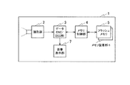
(1)図1、図2、図4に示すように、被写体画像を情報圧縮して間欠記録し、かつ記録媒体として、不揮発性半導体メモリ(フラッシュメモリ)5を使用するビデオカメラ1であって、
前記被写体画像を撮影して得た被写体画像信号を出力する撮影部2と、
前記撮影部2から供給される前記被写体画像信号を情報圧縮するエンコード処理を行いかつ撮影順に論理アドレス10Aを付して得た圧縮画像信号を出力し、また供給される前記圧縮画像信号を前記エンコード処理と相補的にデコード処理をして得た前記画像信号を前記論理アドレス10Aに基づいて出力するエンコード・デコード部(データENC/DEC部)3と、
前記エンコード・デコード部3から出力する前記圧縮画像信号に対して当該メモリ固有の物理アドレス10Bを対応付けて(得た論理/物理アドレス変換テーブル10を)前記不揮発性半導体メモリ5(のアドレス変換テーブルエリア5A)に記憶し、また前記物理アドレス10Bを対応付けて記憶した前記圧縮画像信号を前記不揮発性半導体メモリ5(のアドレス変換テーブルエリア5A)から読み出して前記エンコード・デコード部3側へ出力するために、前記不揮発性半導体メモリ5を装着するメモリ装着部6と、
前記メモリ装着部6に装着された前記不揮発性半導体メモリ5に記憶された前記圧縮画像信号により対応付けられた、各前記論理アドレス10Aと各前記物理アドレス10Bとを一組として、それぞれ順次列記した論理/物理アドレス変換テーブル(アドレス変換テーブル)10を予め作成(フラッシュメモリ5内のアドレス変換テーブルエリア5Aに記憶)しておき、前記不揮発性半導体メモリ5へ前記圧縮画像信号を書き込む際、又は、前記不揮発性半導体メモリ5から前記圧縮画像信号を読み出す際に、キャッシュメモリ(RAM11)内に保存されてある前記論理アドレス10Aと前記物理アドレス10Bの各組を参照して、メモリ制御を行うメモリ制御部4とを、
有することを特徴とするビデオカメラ。
(1) As shown in FIG. 1, FIG. 2, and FIG. 4, a video camera 1 that compresses and intermittently records a subject image and uses a nonvolatile semiconductor memory (flash memory) 5 as a recording medium. ,
A photographing
An encoding process for compressing information on the subject image signal supplied from the
The compressed semiconductor image output from the encoding /
Each logical address 10A and each physical address 10B associated with each other by the compressed image signal stored in the
A video camera comprising:
(2) 前記不揮発性半導体メモリは、NAND型フラッシュメモリであることを特徴とする請求項1に記載のビデオカメラ。 (2) The video camera according to claim 1, wherein the nonvolatile semiconductor memory is a NAND flash memory.
上記した構成を有する本発明によれば、不揮発性半導体メモリからキャッシュメモリへの圧縮画像データの書き込み、読み出しを制御することによって、不揮発性半導体メモリの大記憶容量化に対応してキャッシュメモリの記憶容量を増加させたのと同等の効果を得ることができ、また、読み出しの回数増加によるエラーの発生を未然に抑圧することができ、そして装置本体のコストを低減することができるビデオカメラを提供することができる。 According to the present invention having the above-described configuration, the storage of the cache memory is adapted to the increase in the storage capacity of the nonvolatile semiconductor memory by controlling the writing and reading of the compressed image data from the nonvolatile semiconductor memory to the cache memory. Providing a video camera that can achieve the same effect as increasing the capacity, can suppress the occurrence of errors due to an increase in the number of readouts, and can reduce the cost of the main unit can do.
以下、本発明のビデオカメラの実施の形態を説明する。 Hereinafter, embodiments of the video camera of the present invention will be described.
図1は、本発明のビデオカメラの実施の形態を説明するためのブロック図である。 FIG. 1 is a block diagram for explaining an embodiment of a video camera of the present invention.
ビデオカメラ1は、図1に示すように、撮影部2、データ・エンコード・デコード(ENC/DEC)部3、メモリ制御部4、フラッシュメモリ5を装着するメモリ装着部6、画像表示部7を有している。不揮発性半導体メモリであるフラッシュメモリ5は、NAND型フラッシュメモリである。
As shown in FIG. 1, the video camera 1 includes a
次に、上記した構成を有するビデオカメラ1の記録再生動作について説明する。 Next, the recording / reproducing operation of the video camera 1 having the above configuration will be described.
記録時は、撮影部2は被写体画像を撮影した被写体画像で撮影された画像データは、データENC/DEC部3に送られ、ここでエンコード(情報圧縮)処理されて圧縮画像データとして生成され、この後、撮影順に論理アドレス10Aを付した圧縮画像データは、メモリ制御部4の書き込み制御に応じて、フラッシュメモリ5に書き込まれる。
At the time of recording, the image data captured by the
再生時には、フラッシュメモリ5から読み出された、撮影順に論理アドレス10Aを付した圧縮画像データは、メモリ制御部4の読み出し制御に応じて、データENC/DEC部3に送られ、ここで、前記したエンコード処理と相補的にデコード(情報伸長)処理されて元の画像データとして復元され再生される。データENC/DEC部3で復元された画像データは、画像表示部7に送られ、ここで表示される。
At the time of reproduction, the compressed image data read from the
さてここで、本発明の主要部である、メモリ制御部4とフラッシュメモリ5との関係、即ち、論理アドレスと物理アドレスとの関係について、図2〜図4を用いて説明する。
Now, a relationship between the
図2は論理/物理アドレス変換テーブルを説明するための図、図3は論理/物理アドレス変換のシーケンスを示すフローチャート、図4はフラッシュメモリコントローラの物理アドレス取得部の構成を示す図である。 FIG. 2 is a diagram for explaining a logical / physical address conversion table, FIG. 3 is a flowchart showing a sequence of logical / physical address conversion, and FIG. 4 is a diagram showing a configuration of a physical address acquisition unit of the flash memory controller.
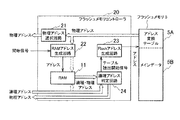
図2及び図4中、5Aはアドレス変換テーブル10(図2)を格納するフラッシュメモリ5内のアドレス変換テーブルエリア、5Bは圧縮データであるメインデータを格納するフラッシュメモリ5内のメインデータエリア、10は論理/物理アドレス変換テーブルであるアドレス変換テーブル、10Aは指定論理アドレス(論理アドレス)、10Bは物理アドレス、11はキャッシュメモリであるRAM、20はフラッシュメモリコントローラ、21は物理アドレス選択回路、22はRAMアドレス選択回路、23はフラッシュアドレス(Frash)生成回路、24は論理アドレス判定回路である。
2 and 4, 5A is an address conversion table area in the
フラッシュメモリ5は、次のように、圧縮データを記憶し、記憶した圧縮データを読み出す。
The
即ち、記録時、データENC/DEC部3から出力する圧縮画像データに対して当該フラッシュメモリ固有の物理アドレス10Bを対応付けてこれを記憶する。図2に示すように、例えば、圧縮画像データに順次付されている論理アドレス10Aが「0」、「1」、「2」、「3」、「4」、「5」のとき、物理アドレス10Bはそれぞれ、「2」、「3」、「5」、「11」、「7」「13」と対応付ける。
That is, at the time of recording, the compressed image data output from the data ENC /
また再生時には、この物理アドレス10Bを対応付けて記憶した圧縮画像信号をここから読み出して、データENC/DEC部3側へ出力する。
Further, at the time of reproduction, the compressed image signal stored in association with the physical address 10B is read from here and output to the data ENC /
前記メモリ制御部4は、次のように、フラッシュメモリ5の書き込み、読み出し動作を制御する。
The
即ち、フラッシュメモリ5に記憶された圧縮画像信号により対応付けられた論理アドレスと当該フラッシュメモリ固有の物理アドレスとを一組(図2に示すように、例えば、論理アドレス「1」と物理アドレス「3」とを一組)として、それぞれ順次列記した論理/物理アドレス変換テーブル(アドレス変換テーブル10)を予め、フラッシュメモリ5内のアドレス変換テーブルエリア5Aに作成して格納しておく。
That is, a set of a logical address associated with the compressed image signal stored in the
この後、フラッシュメモリ5のメインデータエリア5Bへ圧縮画像信号を書き込む際、又は、フラッシュメモリ5のメインデータエリア5Bから圧縮画像信号を読み出す際に、まず、キャッシュメモリであるRAM11(図2)を参照する。
Thereafter, when writing the compressed image signal to the main data area 5B of the
そして、前記論理アドレスに対して前記物理アドレスが変更されている組がある場合(図2に示すように、論理アドレス「1」と物理アドレス「3」との関係がない場合)には、当該組に優先して、前記論理アドレスに対して前記物理アドレスが変更されていない組(図2に示すように、論理アドレス「2」と物理アドレス「5」の組、論理アドレス「3」と物理アドレス「11」の組、論理アドレス「4」と物理アドレス「7」の組、論理アドレス「5」と物理アドレス「13」の組)を抽出してこれを使用する(RAM11を使用するキャッシュメモリに書き込む)メモリ制御を、メモリ制御部4は行う。
When there is a pair in which the physical address is changed with respect to the logical address (when there is no relationship between the logical address “1” and the physical address “3” as shown in FIG. 2), Prior to the set, the set in which the physical address is not changed with respect to the logical address (as shown in FIG. 2, the set of logical address “2” and physical address “5”, logical address “3” and physical A set of address “11”, a set of logical address “4” and physical address “7”, and a set of logical address “5” and physical address “13”) are extracted and used (cache memory using RAM 11) The
上記したことをさらに詳しく説明する。 The above will be described in more detail.
図2に示すように、フラッシュメモリ5内のアドレス変換テーブルエリア5A(図4)には、アドレス変換テーブル10が設けられている。また、上記メモリ制御部4であるフラッシュメモリコントローラ20内のRAM11(図4)には、論理アドレス順に対応する物理アドレスが格納されている。
As shown in FIG. 2, an address conversion table 10 is provided in the address
図2に示すように、論理アドレス10Aと物理アドレス10Bとの対応関係は次のようである。 As shown in FIG. 2, the correspondence between the logical address 10A and the physical address 10B is as follows.
論理アドレス「0」−物理アドレス「2」、
論理アドレス「1」−物理アドレス「3」、
論理アドレス「2」−物理アドレス「5」、
論理アドレス「3」−物理アドレス「11」、
論理アドレス「4」−物理アドレス「7」、
論理アドレス「5」−物理アドレス「13」、
が、それぞれ各組となっている。
Logical address “0” —physical address “2”,
Logical address “1” —physical address “3”,
Logical address “2” —physical address “5”,
Logical address “3” —physical address “11”,
Logical address “4” —physical address “7”,
Logical address “5” —physical address “13”,
However, each is in each group.
ここで、外部から論理アドレス「2」が指定された場合、対応する物理アドレス「5」を出力することになるが、この時、論理アドレス「2」−物理アドレス「5」の組に加えて、論理アドレス「3」−物理アドレス「11」の組、論理アドレス「4」−物理アドレス「7」の組、そして、論理アドレス「5」−物理アドレス「13」の組もRAM11に書き込む。
Here, when the logical address “2” is designated from the outside, the corresponding physical address “5” is output. At this time, in addition to the combination of the logical address “2” and the physical address “5” The logical address “3” -physical address “11” pair, the logical address “4” -physical address “7” pair, and the logical address “5” -physical address “13” pair are also written in the
このように、複数の論理/物理アドレスの各組をRAM11に保存しておくことにより、次回以降、論理/物理アドレスの変換が必要となった時に、フラッシュメモリ5内のアドレス変換テーブル10を全て読み出さなくても済む確率が増し、これによって本来扱うデータのリードやライトのパフォーマンスが向上する。
In this way, by storing each set of a plurality of logical / physical addresses in the
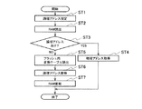
図3は、本発明の実施の形態に係る論理/物理アドレス変換のシーケンスを示している。 FIG. 3 shows a sequence of logical / physical address conversion according to the embodiment of the present invention.
フラッシュメモリコントローラ20は、アクセスする論理アドレスを外部から指定されたら(ステップST1)、論理アドレスと物理アドレスの組が保存されているRAM11内のデータを読み出し(ステップST2)、指定された論理アドレスが存在するかを検索する(ステップST3)。
When the logical address to be accessed is designated from the outside (step ST1), the
この検索の結果、指定された論理アドレスが検出された場合は、対応する物理アドレスを外部へ出力する(ステップST4)。一方、指定された論理アドレスが検出されなかった場合には、フラッシュメモリ5内のアドレス変換テーブル10(5A)を読み出し(ステップST5)、対応する物理アドレスを外部へ出力する(ステップST6)とともに、RAM11内のデータを更新する(ステップST7)。
If the designated logical address is detected as a result of this search, the corresponding physical address is output to the outside (step ST4). On the other hand, when the designated logical address is not detected, the address conversion table 10 (5A) in the
ここで、図4に示すフラッシュメモリコントローラの物理アドレス取得部について説明する。 Here, the physical address acquisition unit of the flash memory controller shown in FIG. 4 will be described.
図4において、フラッシュメモリコントローラ20の物理アドレス取得部は、RAMアドレス生成回路22、RAM11、論理アドレス判定回路24、Flashアドレス生成回路23、物理アドレス選択回路21を有する。
In FIG. 4, the physical address acquisition unit of the
RAMアドレス生成回路22では、外部からの論理/物理アドレス変換の開始信号を受け、RAM11に対してデータを読み出すコマンドやアドレスを出力する。また、フラッシュメモリ5からアドレス変換テーブル10(5A)が読み出された際には、外部からの論理アドレスとフラッシュからの物理アドレスを組にしたものをRAM11に書き込むためのコマンドやアドレスを出力する(図2参照)。
The RAM
論理アドレス判定回路24では、RAM11から読み出されたデータの中に外部から指定された論理アドレスが存在するかを確認する。指定された論理アドレスが存在した場合は、論理/物理アドレス変換完了とし、外部に対して対応する物理アドレスを出力する。一方、指定された論理アドレスが存在しなかった場合は、Flashアドレス生成回路23に対してアドレス変換テーブル10(5A)の読み出し開始信号を出力する。
The logical
Flashアドレス生成回路23では、論理アドレス判定回路24からのアドレス変換テーブルの読み出し開始信号を受け、フラッシュメモリ5に対してアドレス変換テーブル10(5A)を読み出すコマンドやアドレスを出力する。
In response to the address conversion table read start signal from the logical
物理アドレス選択回路21では、フラッシュメモリ5から読み出されたデータの中から指定された論理アドレスに対応する物理アドレスを選択し、外部に対してその物理アドレスを出力する。
The physical
1 ビデオカメラ
2 撮影部
3 データENC/DEC部(エンコード・デコード部)
4 メモリ制御部
5 フラッシュメモリ(不揮発性半導体メモリ)
5A アドレス変換テーブルエリア
6 メモリ装着部
10 アドレス変換テーブル(論理/物理アドレス変換テーブル)
10A 前記論理アドレス
10B 物理アドレス
11 RAM(キャッシュメモリ)
1
4
5A Address conversion table area 6 Memory mounting unit 10 Address conversion table (logical / physical address conversion table)
10A Logical address 10B
Claims (2)
前記被写体画像を撮影して得た被写体画像信号を出力する撮影部と、
前記撮影部から供給される前記被写体画像信号を情報圧縮するエンコード処理を行いかつ撮影順に論理アドレスを付して得た圧縮画像信号を出力し、また供給される前記圧縮画像信号を前記エンコード処理と相補的にデコード処理をして得た前記画像信号を前記論理アドレスに基づいて出力するエンコード・デコード部と、
前記エンコード・デコード部から出力する前記圧縮画像信号に対して当該メモリ固有の物理アドレスを対応付けて前記不揮発性半導体メモリに記憶し、また前記物理アドレスを対応付けて記憶した前記圧縮画像信号を前記不揮発性半導体メモリから読み出して前記エンコード・デコード部側へ出力するために、前記不揮発性半導体メモリを装着するメモリ装着部と、
前記メモリ装着部に装着された前記不揮発性半導体メモリに記憶された前記圧縮画像信号により対応付けられた、各前記論理アドレスと各前記物理アドレスとを一組として、それぞれ順次列記した論理/物理アドレス変換テーブルを予め作成しておき、前記不揮発性半導体メモリへ前記圧縮画像信号を書き込む際、又は、前記不揮発性半導体メモリから前記圧縮画像信号を読み出す際に、キャッシュメモリ内に保存されてある前記論理アドレスと前記物理アドレスの各組を参照して、メモリ制御を行うメモリ制御部とを、
有することを特徴とするビデオカメラ。 A video camera that compresses a subject image and intermittently records it, and uses a nonvolatile semiconductor memory as a recording medium,
A photographing unit for outputting a subject image signal obtained by photographing the subject image;
Encoding processing for compressing information on the subject image signal supplied from the imaging unit and outputting a compressed image signal obtained by assigning logical addresses in the order of imaging, and the supplied compressed image signal as the encoding processing An encoding / decoding unit that outputs the image signal obtained by complementary decoding based on the logical address;
The compressed image signal output from the encoding / decoding unit is stored in the nonvolatile semiconductor memory in association with a physical address unique to the memory, and the compressed image signal stored in association with the physical address is stored in the non-volatile semiconductor memory. In order to read from the nonvolatile semiconductor memory and output to the encoding / decoding unit side, a memory mounting unit for mounting the nonvolatile semiconductor memory,
Logical / physical addresses sequentially listed as a set of each logical address and each physical address associated with each other by the compressed image signal stored in the nonvolatile semiconductor memory mounted in the memory mounting unit The logic stored in the cache memory when a conversion table is created in advance and the compressed image signal is written to the nonvolatile semiconductor memory or when the compressed image signal is read from the nonvolatile semiconductor memory. A memory control unit that performs memory control with reference to each set of addresses and physical addresses,
A video camera comprising:
Priority Applications (1)
| Application Number | Priority Date | Filing Date | Title |
|---|---|---|---|
| JP2007249455A JP2009081663A (en) | 2007-09-26 | 2007-09-26 | Video camera |
Applications Claiming Priority (1)
| Application Number | Priority Date | Filing Date | Title |
|---|---|---|---|
| JP2007249455A JP2009081663A (en) | 2007-09-26 | 2007-09-26 | Video camera |
Publications (1)
| Publication Number | Publication Date |
|---|---|
| JP2009081663A true JP2009081663A (en) | 2009-04-16 |
Family
ID=40656098
Family Applications (1)
| Application Number | Title | Priority Date | Filing Date |
|---|---|---|---|
| JP2007249455A Pending JP2009081663A (en) | 2007-09-26 | 2007-09-26 | Video camera |
Country Status (1)
| Country | Link |
|---|---|
| JP (1) | JP2009081663A (en) |
-
2007
- 2007-09-26 JP JP2007249455A patent/JP2009081663A/en active Pending
Similar Documents
| Publication | Publication Date | Title |
|---|---|---|
| JP4392601B2 (en) | Data access device and recording medium | |
| US7917687B2 (en) | Flash memory apparatus and access method to flash memory | |
| US20110035539A1 (en) | Storage device, and memory controller | |
| US20130073816A1 (en) | Method of storing data in a storage medium and data storage device including the storage medium | |
| US8750679B2 (en) | Information processing apparatus, recording method, and computer program | |
| US20190243754A1 (en) | Flash fast program mode for high definition video recording and high resolution camera burst mode recording | |
| TW200636747A (en) | Method and system for storing logical data blocks into flash-blocks in multiple non-volatile memories which are connected to at least one common data I/O bus | |
| US20090135256A1 (en) | Sata camera system | |
| JP5374254B2 (en) | Image file transfer device | |
| US20110022774A1 (en) | Cache memory control method, and information storage device comprising cache memory | |
| JP2001189915A (en) | Recording device | |
| CN101425310B (en) | Method to reserve index storage space during audio video interleaved recording | |
| US6904492B2 (en) | Write-once memory device including non-volatile memory for temporary storage | |
| US8151150B2 (en) | Data storage device and method for writing test data to a memory | |
| JP4158774B2 (en) | Playback method | |
| TWI308459B (en) | Context-aware frame memory scheme for motion compensation in video decoding | |
| JP2009081663A (en) | Video camera | |
| CA2619344C (en) | Content data storage device and its control method | |
| US11082168B1 (en) | Entropy driven endurance for normalized quality of service | |
| CN1932780B (en) | Recording control device and recording control method | |
| JP2000276856A (en) | Data recording device, data recording method, data reproducing device, and data reproducing method | |
| JP2021044673A (en) | Video server device and video data writing/reading method | |
| JP4972909B2 (en) | Data recording device | |
| JP3317169B2 (en) | Decoding and reproducing apparatus for digitally compressed data | |
| JP2007279873A (en) | Data recording device |