JP2009077565A - Semiconductor device for switching power supply application - Google Patents
Semiconductor device for switching power supply application Download PDFInfo
- Publication number
- JP2009077565A JP2009077565A JP2007244848A JP2007244848A JP2009077565A JP 2009077565 A JP2009077565 A JP 2009077565A JP 2007244848 A JP2007244848 A JP 2007244848A JP 2007244848 A JP2007244848 A JP 2007244848A JP 2009077565 A JP2009077565 A JP 2009077565A
- Authority
- JP
- Japan
- Prior art keywords
- switching
- power supply
- circuit
- period
- transformer
- Prior art date
- Legal status (The legal status is an assumption and is not a legal conclusion. Google has not performed a legal analysis and makes no representation as to the accuracy of the status listed.)
- Withdrawn
Links
Images


Abstract
Description
本発明は、スイッチング電源用半導体装置に関し、特に、無負荷あるいは軽負荷時における消費電力を削減できるスイッチング電源用半導体装置に関するものである。 The present invention relates to a semiconductor device for switching power supply, and more particularly to a semiconductor device for switching power supply that can reduce power consumption at no load or light load.
従来のスイッチング電源用半導体装置の一例を図7に示す。従来、電子機器用電源装置の一種として、商用電源であるDC入力端子10を1次側とし、電子機器の駆動部になる出力端子15を2次側とし、1次側と2次側をつなぐトランス(変圧器)11を持ち、1次側にパワーMOSFET等とそのスイッチング制御回路18からなるスイッチング素子を有するスイッチング電源が一般的に用いられている。このスイッチング電源は、無負荷時あるいは軽負荷時は、入力電力に対する、スイッチング損失など電源回路内での消費電力の割合が増加するため、効率が悪くなる。そこでスイッチング損失を低減し、電源回路内部での消費電力を削減するために、間欠動作をさせることがある。負荷に応じて発振数を減少させることにより、スイッチング損失を低減し、効率を改善させる。以下に、従来の間欠動作の制御方法を示す。
An example of a conventional semiconductor device for switching power supply is shown in FIG. Conventionally, as a kind of power supply device for electronic equipment, a
例えば、負荷電流が小さくなるに従い、スイッチング素子がオンとなる時間を遅らせる遅延回路を、スイッチング素子を駆動させる巻線に接続させることにより、最小負荷時のスイッチング素子の時間あたりのスイッチング損失を下げて、最小負荷時の効率を大幅に改善する制御方法がある(特許文献1参照)。 For example, as the load current decreases, a delay circuit that delays the time when the switching element is turned on is connected to the winding that drives the switching element, thereby reducing the switching loss per hour of the switching element at the minimum load. There is a control method that greatly improves the efficiency at the minimum load (see Patent Document 1).
また、例えば、スイッチング電源が無負荷あるいは軽負荷時であるときに、スイッチング動作において動作状態と停止状態を繰り返す間欠動作モードの制御方法がある(特許文献2参照)。 Further, for example, there is a control method of an intermittent operation mode in which an operation state and a stop state are repeated in a switching operation when the switching power supply is at no load or light load (see Patent Document 2).
また、一般的なスイッチング電源では、高入力時にスイッチング素子であるパワーMOSFETがスイッチングオフした際に、パワーMOSFETのトランスの1次巻線側の電位が跳ね上がり(スパイク電圧)、パワーMOSFETが破壊することを防ぐためにスパイク電圧をクランプする回路(スナバ回路)16を設けている。
前記従来のスイッチング電源用半導体装置では、待機時あるいは軽負荷時の間欠発振動作中のスイッチング損失は低減されるものの、スナバ回路での電力消費は考慮されていない。 In the conventional switching power supply semiconductor device, although the switching loss during the intermittent oscillation operation during standby or light load is reduced, power consumption in the snubber circuit is not taken into consideration.
本発明は、スナバ回路での電力消費を減少させることにより、前記の従来例よりさらに消費電力を削減し、待機時および軽負荷時の電源効率を向上するスイッチング電源用半導体装置を提供することを目的とするものである。 It is an object of the present invention to provide a semiconductor device for a switching power supply that reduces the power consumption in the snubber circuit, thereby further reducing the power consumption compared with the conventional example and improving the power supply efficiency during standby and light loads. It is the purpose.
上記目的を達成するために、本発明は、スイッチング制御回路を設け、軽負荷時には所定の周期で軽負荷スイッチング信号を発生させ、間欠発振を行い、1回の間欠発振のオン期間における発振数を増加させ、オフ期間が長くなるように制御することで、スナバ回路で消費される電力を減少させる。 In order to achieve the above object, the present invention provides a switching control circuit, generates a light load switching signal at a predetermined period at light load, performs intermittent oscillation, and sets the number of oscillations in the on period of one intermittent oscillation. The power consumed by the snubber circuit is reduced by increasing the off period and controlling the off period.
本発明のスイッチング電源用半導体装置は、変圧器と、第一の直流電圧を発生する電圧源に接続された変圧器の1次巻線をスイッチング駆動するスイッチング素子と、変圧器の1次巻線の高圧側に並列接続した容量と抵抗の一端を接続し、その並列な容量と抵抗の逆端にツェナーダイオードのカソードを接続し、ツェナーダイオードのアノードを変圧器の1次巻線の低圧側に接続したスナバ回路と、変圧器の2次巻線と接続され、変圧器の2次側出力電圧を整流し、且つ平滑化することにより第2の直流電圧を生成して出力する出力電圧生成回路と、スイッチング素子の動作を制御するスイッチング制御回路と、出力電圧の誤差を前記スイッチング制御回路にフィードバックする出力電圧の誤差検出回路を備えたスイッチング電源装置を制御するスイッチング電源用半導体装置を対象とする。 A semiconductor device for a switching power supply according to the present invention includes a transformer, a switching element for switching and driving a primary winding of a transformer connected to a voltage source that generates a first DC voltage, and a primary winding of the transformer. Connect one end of the resistor and the resistor connected in parallel to the high-voltage side of the capacitor, connect the cathode of the Zener diode to the opposite end of the parallel capacitor and resistor, and connect the anode of the Zener diode to the low-voltage side of the primary winding of the transformer An output voltage generation circuit which is connected to the connected snubber circuit and the secondary winding of the transformer, and generates and outputs a second DC voltage by rectifying and smoothing the secondary output voltage of the transformer And a switching control circuit that controls the operation of the switching element, and a switching power supply device that includes an output voltage error detection circuit that feeds back an output voltage error to the switching control circuit. Target semiconductor device for a switching power supply that.
本発明では、無負荷時あるいは軽負荷時の間欠発振動作において、1回のスイッチングオン期間での発振数を増加させ、スイッチングオフ期間を延長させることにより、単位時間当たりにスナバ回路で消費される電力を減少させ、無負荷時あるいは軽負荷時のスイッチング電源回路の電源効率を向上させることができる。 In the present invention, the power consumed by the snubber circuit per unit time is increased by increasing the number of oscillations in one switching on period and extending the switching off period in intermittent oscillation operation at no load or light load. And the power supply efficiency of the switching power supply circuit at the time of no load or light load can be improved.
(実施の形態1)
以下、本発明の実施の形態1について、図面を参照しながら説明する。
(Embodiment 1)
図1は本発明の1実施の形態に係るスイッチング電源装置の概略的な回路構成を示している。図1に示すように、第1の実施形態に係るスイッチング電源装置は、入力端子10に印加された直流電圧を、トランス(変圧器)11の1次側に印加しながら、スイッチング素子12によるスイッチング動作によって、トランス11の2次側に設けられた出力電圧生成回路14により第2の直流電圧である出力電圧Voにまで降下して出力端子15に出力するスイッチング電源装置である。また、スイッチング素子12のターンオフに伴い、トランス11の1次巻線11aにおけるスイッチング素子12側の電圧の跳ね上がりによりスイッチング素子12の破壊を防ぐために、トランス11の1次巻線11aと並列にスナバ回路16が設けられている。次に、フィードバック方法について以下に記述する。出力電圧生成回路14の高電位側の端子と低電位側の端子の間に出力電圧の誤差検出回路17とフィードバック回路13が接続されている。図1ではフィードバック回路にフォトカプラを用いている。出力電圧の誤差検出回路17を流れる電流値は出力電圧に比例する。出力電圧の誤差検出回路17と直列に挿入したフォトカプラ13の発光ダイオード13aに出力電圧に比例した電流が流れ、フォトカプラ13の発光ダイオード13aが光り、一次側のフォトカプラ13の出力トランジスタ13bに電流が流れ、スイッチング素子のスイッチング調整回路19のフィードバック端子から流出する。スイッチング調整回路19はフィードバック端子から流出した電流値を検知し、スイッチング動作による2次側への電力供給の増減を制御する。2次側への供給電力が過剰となり、出力電圧生成回路14の出力電圧が上昇した場合は、フィードバック端子から流出する電流の増加を検知し、供給電力を減少させるように制御し、逆に供給電力が不足し、出力電圧生成回路14の出力電圧が低下するとフィードバック端子から流出する電流が減少することを検知し、供給電力を増加させるように働く。供給電力の増減を制御する方法としては、トランス11の1次巻線11aを流れる電流のピーク値を制御する方法や、周波数を変化させて単位時間当たりの発振数を制御する方法などが考えられる。以上の制御方法を繰り返し、フィードバック電流が安定する方向に収束する。
FIG. 1 shows a schematic circuit configuration of a switching power supply apparatus according to an embodiment of the present invention. As shown in FIG. 1, the switching power supply according to the first embodiment is switched by a
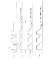
以上は、通常の負荷条件でのフィードバック方法であるが、無負荷あるいは軽負荷時では、スイッチング調整回路19内で軽負荷検出回路によりスイッチング方式が間欠動作に切り替わり、スイッチング制御回路18内でスイッチングオン期間信号を生成し、スイッチングオン期間信号がオンのときのみ、スイッチング動作を行う。無負荷時あるいは軽負荷時は、スイッチング制御回路18は供給電力を低下させる方向に働き、供給電力がある一定値に達するとスイッチングオン期間信号がオフし、スイッチング動作を停止され、オフ期間に入る。供給電力がゼロになるため、出力電圧が低下し始め、フィードバック端子から流出する電流が減少し、ある値に達すると再びスイッチングオン期間信号がオンに切り替わり、スイッチング制御回路18がパワーMOSFETにスイッチング信号を送りスイッチング動作を開始し、オン期間に移行する。オン期間に入り電力供給が始まると、出力電力が過剰になるため、スイッチング制御回路は供給電力を減少させる方向に働き、再びオフ期間に移行する。以上を繰り返し、間欠発振動作を行う。この間欠発振動作時のスイッチング信号とトランス11の1次巻線11aを流れる電流波形を図8に示す。またこの時の間欠発振の波形を図9に示す。図9は、スイッチング電源においてトランスの1次巻線からスイッチング素子に流れる電流IDSと1次巻線のスイッチング素子側の電圧VDSの波形(a)と、スナバ回路の容量CSBと抵抗RSBにかかる電圧VSBの波形(b)と、スナバ回路の抵抗RSBに流れる電流IRSBの波形(c)と、スナバ回路の抵抗RSBで消費される電力PRSBの波形(d)である。
The above is a feedback method under normal load conditions, but when there is no load or light load, the switching method is switched to intermittent operation by the light load detection circuit in the
本発明では、このスイッチング制御回路18内でパワーMOSFET12とスイッチング調整回路19の間に、間欠発振スイッチング信号のオン期間を延長させる遅延回路20を挿入する。
In the present invention, a
この場合、1回のオン期間の発振数が増加し、2次側へ供給されるエネルギーが増加するため、スイッチング素子がオフした後、次の発振までのオフ期間が長くなる。 In this case, the number of oscillations in one on period increases and the energy supplied to the secondary side increases, so that the off period until the next oscillation becomes longer after the switching element is turned off.
まず、図2は、遅延回路によりオン期間が長くなり、1回のオン期間あたりの発振数が増加した場合(図2は発振数が3の場合)のトランス11の1次巻線11aを流れる電流波形(a)とスイッチング信号(b)と遅延回路20を通したスイッチングオン期間信号(c)である。またこの時の間欠発振の波形を図3に示す。図3は、スイッチング電源においてトランスの1次巻線からスイッチング素子に流れる電流IDSと1次巻線のスイッチング素子側の電圧VDSの波形(a)と、スナバ回路の容量CSBと抵抗RSBにかかる電圧VSBの波形(b)と、スナバ回路の抵抗RSBに流れる電流IRSBの波形(c)と、スナバ回路の抵抗RSBで消費される電力PRSBの波形(d)である。スイッチング素子がターンオフした際に、1次巻線のスイッチング素子側の電圧VDSが、2次側の反射電圧VOR分だけ跳ね上がる。2次側に電流が流れている期間(1)では、反射電圧VORがスナバ回路にかかる。この期間(1)にスナバ回路の抵抗RSBで消費されるエネルギーは、
First, in FIG. 2, when the ON period becomes longer due to the delay circuit and the number of oscillations per one ON period increases (FIG. 2 shows the case where the number of oscillations is 3), the current flows through the primary winding 11a of the transformer 11. A current waveform (a), a switching signal (b), and a switching on period signal (c) through the

となる。また、フライバック電源は非連続モードで発振するため、2次側電流がゼロまで減衰した後、スナバ回路にかかる電圧はゼロとなり、スナバ回路の容量CSBに蓄積されていた電力が放出され、スナバ回路の抵抗で消費される電力は、 It becomes. In addition, since the flyback power supply oscillates in a discontinuous mode, the voltage applied to the snubber circuit becomes zero after the secondary current is attenuated to zero, and the power stored in the snubber circuit capacitor C SB is released. The power consumed by the snubber circuit resistance is
となる。 It becomes.
本発明では、スイッチング電源の間欠発振時に、オン期間が長くなる遅延回路を挿入し、1回のオン期間あたりの発振数を増加させ、オン期間中は発振でスナバ回路の容量CSBに蓄積された電力がすべて放出される前に次発振が起こり、オン期間後の次の発振までのオフ期間を長くする構成にすることにより、このスナバ回路における電力損失のうち、ii)のスナバ回路の容量に蓄積された電力消費を減少させる。 In the present invention, during intermittent oscillation of the switching power supply, a delay circuit that increases the on period is inserted to increase the number of oscillations per on period, and during the on period, oscillation is accumulated in the capacitor C SB of the snubber circuit. The second oscillation occurs before all the power is released, and the off-period until the next oscillation after the on-period is lengthened to increase the capacity of the snubber circuit in ii) of the power loss in this snubber circuit. Reduce the power consumption stored in the.
以下に、消費電力の計算式を示す。 The formula for calculating power consumption is shown below.
まず、スナバ回路の容量CSBと抵抗RSBにかかる電圧VSBを計算する。二次側に電流が流れ、電力が消費されている期間(1)では、VSBは反射電圧VORとなる。この期間(1)で消費されるエネルギーは上式i)と同様である。間欠発振時は、フライバック電源は非連続モードで発振するため、2次側電流がゼロまで減衰すると、スナバ回路にかかっていた反射電圧もゼロに減衰するが、スナバ回路の容量に蓄積された電力が放出される期間(2)はスナバ回路の抵抗に電流が流れるため、スナバ回路の抵抗にかかる電圧VSBは以下の式iii)になる。 First, calculate the voltage V SB according to the capacitance C SB and the resistance R SB of the snubber circuit. In the period (1) in which current flows on the secondary side and power is consumed, V SB becomes the reflected voltage V OR . The energy consumed in this period (1) is the same as in the above equation i). During intermittent oscillation, the flyback power supply oscillates in discontinuous mode, so when the secondary current decays to zero, the reflected voltage applied to the snubber circuit also decays to zero, but is stored in the snubber circuit capacitance. In the period (2) during which power is released, current flows through the snubber circuit resistance, so the voltage V SB applied to the snubber circuit resistance is expressed by the following equation iii).
ここで、一回あたりのオン期間の発振数をn回とすると、そのオン期間にスナバ回路で消費される電力は以下のiv)式になる。 Here, when the number of oscillations in the on period per time is n, the power consumed by the snubber circuit in the on period is expressed by the following equation iv).
上記iv)式において、t>0の場合、 In the above formula iv), when t> 0,
![]()
![]()
となるため、nが大きいほど、スナバ回路で消費される電力PRBSは小さくなる。 Therefore, as n increases, the power PRBS consumed in the snubber circuit decreases.
なお、無負荷時あるいは軽負荷時の間欠発振制御については、フィードバック端子への電流のヒステリシスにより、オン期間とオフ期間を繰り返す制御方式で説明したが、周波数を変動させることにより、単位時間当たりの発振回数を変動させて、供給電力を制御する方式でも可能である。 Note that the intermittent oscillation control at no load or light load has been explained by the control method that repeats the on period and the off period due to the hysteresis of the current to the feedback terminal, but by changing the frequency, oscillation per unit time A method of controlling the power supply by changing the number of times is also possible.
なお、その他の間欠発振制御方式でも可能である。 Other intermittent oscillation control methods are also possible.
なお、図中の回路はフライバック方式のスイッチング電源回路であるが、フォワード方式のスイッチング電源回路でも可能である。 Although the circuit in the figure is a flyback switching power supply circuit, a forward switching power supply circuit is also possible.
なお、フィードバック回路13に関しては、図中ではフォトカプラを用いているが、他のフィードバック方式でも可能である。
As for the
(実施の形態2)
以下、本発明の実施の形態2について、図面を参照しながら説明する。
(Embodiment 2)
図4は本発明の1実施の形態に係るスイッチング電源装置の概略的な回路構成を示している。図4に示すように、第2の実施形態に係るスイッチング電源装置は、入力端子10に印加された直流電圧を、トランス(変圧器)11の1次側に印加しながら、スイッチング素子12によるスイッチング動作によって、トランス11の2次側に設けられた出力電圧生成回路14により第2の直流電圧である出力電圧Voにまで降下して出力端子15に出力するスイッチング電源装置である。また、スイッチング素子12のターンオフに伴い、トランス11の1次巻線11aにおけるスイッチング素子12側の電圧の跳ね上がりによりスイッチング素子12の破壊を防ぐために、トランス11の1次巻線11aと並列にスナバ回路16が設けられている。次に、フィードバック方法について以下に記述する。出力電圧生成回路14の高電位側の端子と低電位側の端子の間に出力電圧の誤差検出回路17とフィードバック回路13が接続されている。図4ではフィードバック回路にフォトカプラを用いている。出力電圧の誤差検出回路17を流れる電流値は出力電圧に比例する。出力電圧の誤差検出回路17と直列に挿入したフォトカプラ13の発光ダイオード13aに出力電圧に比例した電流が流れ、フォトカプラ13の発光ダイオード13aが光り、一次側のフォトカプラ13の出力トランジスタ13bに電流が流れ、スイッチング素子のスイッチング調整回路19のフィードバック端子から流出する。スイッチング調整回路19はフィードバック端子から流出した電流値を検知し、スイッチング動作による2次側への電力供給の増減を制御する。2次側への供給電力が過剰となり、出力電圧生成回路14の出力電圧が上昇した場合は、フィードバック端子から流出する電流の増加を検知し、供給電力を減少させるように制御し、逆に供給電力が不足し、出力電圧生成回路14の出力電圧が低下するとフィードバック端子から流出する電流が減少することを検知し、供給電力を増加させるように働く。供給電力の増減を制御する方法としては、トランス11の1次巻線11aを流れる電流のピーク値を制御する方法や、周波数を変化させて単位時間当たりの発振数を制御する方法などが考えられる。以上の制御方法を繰り返し、フィードバック電流が安定する方向に収束する。
FIG. 4 shows a schematic circuit configuration of a switching power supply device according to an embodiment of the present invention. As shown in FIG. 4, the switching power supply according to the second embodiment is switched by the switching
以上は、通常の負荷条件でのフィードバック方法であるが、無負荷あるいは軽負荷時では、スイッチング調整回路19内で軽負荷検出回路によりスイッチング方式が間欠動作に切り替わり、スイッチング制御回路18内でスイッチングオン期間信号を生成し、スイッチングオン期間信号がオンのときのみ、スイッチング動作を行う。無負荷時あるいは軽負荷時は、スイッチング制御回路18は供給電力を低下させる方向に働き、供給電力がある一定値に達するとスイッチングオン期間信号がオフし、スイッチング動作を停止され、オフ期間に入る。供給電力がゼロになるため、出力電圧が低下し始め、フィードバック端子から流出する電流が減少し、ある値に達すると再びスイッチングオン期間信号がオンに切り替わり、スイッチング制御回路18がパワーMOSFETにスイッチング信号を送りスイッチング動作を開始し、オン期間に移行する。オン期間に入り電力供給が始まると、出力電力が過剰になるため、スイッチング制御回路は供給電力を減少させる方向に働き、再びオフ期間に移行する。以上を繰り返し、間欠発振動作を行う。この間欠発振動作時のスイッチング信号とトランス11の1次巻線11aを流れる電流波形を図8に示す。またこの時の間欠発振の波形を図9に示す。図9は、スイッチング電源においてトランスの1次巻線からスイッチング素子に流れる電流IDSと1次巻線のスイッチング素子側の電圧VDSの波形(a)と、スナバ回路の容量CSBと抵抗RSBにかかる電圧VSBの波形(b)と、スナバ回路の抵抗RSBに流れる電流IRSBの波形(c)と、スナバ回路の抵抗RSBで消費される電力PRSBの波形(d)である。
The above is a feedback method under normal load conditions, but when there is no load or light load, the switching method is switched to intermittent operation by the light load detection circuit in the switching
本発明では、このスイッチング制御回路18の中に、間欠時にスイッチング回数をカウントするスイッチングカウンタ21を含み、間欠発振時にスイッチングオン期間に切り替わるとスイッチング回数のカウントをスタートし、設定された最低スイッチング回数に達するまで、オフ期間に移行しないように制御する。 In the present invention, the switching control circuit 18 includes a switching counter 21 that counts the number of times of switching when intermittent, and starts counting the number of times of switching when switching to the switching-on period during intermittent oscillation. It controls so that it does not shift to an off period until it reaches.
この場合、上記のフィードバック電流のヒステリシスによる間欠発振を行った場合の1回のオン時間の発振数より、設定された最低発振数が大きい場合は、1回のオン期間に2次側へ供給されるエネルギーが増加するため、オフ期間に切り替わった後、次の発振までのオフ期間が長くなる。 In this case, if the set minimum number of oscillations is larger than the number of oscillations in one on-time when intermittent oscillation is performed by the hysteresis of the feedback current described above, it is supplied to the secondary side in one on period. Therefore, after switching to the off period, the off period until the next oscillation becomes longer.
また、上記のフィードバック電流のヒステリシスによる間欠発振を行った場合の1回のオン時間の発振数より、設定された最低発振数が小さい場合もしくは同数の場合は、1回のオン期間に2次側へ供給されるエネルギーや、オフ期間に変化はない。 If the set minimum oscillation number is smaller than or equal to the number of oscillations during one on-time when the above-described feedback current hysteresis is performed by the hysteresis of the feedback current, the secondary side is turned on during the one on-period. There is no change in the energy supplied to or off period.
まず、図5は、上記のフィードバック電流のヒステリシスによる間欠発振を行った場合の1回のオン時間の発振数が3回以下であり、かつ設定された最低発振数が3回であった場合、もしくは上記のフィードバック電流のヒステリシスによる間欠発振を行った場合の1回のオン時間の発振数が3回であり、かつ設定された最低発振数が3回以下であった場合に、1回のオン時間の発振数が3回となる間欠発振を行ったときのトランス1次巻線11aの電流波形(a)と、スイッチング信号(b)と、スイッチングカウンタ21でのカウント数(c)を示した図である。またこの時の間欠発振の波形を図3に示す。図3は、この時のスイッチング電源においてトランスの1次巻線からスイッチング素子に流れる電流IDSと1次巻線のスイッチング素子側の電圧VDSの波形(a)と、スナバ回路の容量CSBと抵抗RSBにかかる電圧VSBの波形(b)と、スナバ回路の抵抗RSBに流れる電流IRSBの波形(c)と、スナバ回路の抵抗RSBで消費される電力PRSBの波形(d)である。スイッチング素子がターンオフした際に、1次巻線のスイッチング素子側の電圧VDSが、2次側の反射電圧VOR分だけ跳ね上がる。2次側に電流が流れている期間(1)では、反射電圧VORがスナバ回路にかかる。この期間(1)にスナバ回路の抵抗RSBで消費されるエネルギーは、 First, FIG. 5 shows a case where the number of oscillations in one on-time when the intermittent oscillation by the hysteresis of the feedback current is performed is 3 times or less and the set minimum number of oscillations is 3. Alternatively, when intermittent oscillation is performed with the above feedback current hysteresis, the number of oscillations in one on-time is three, and the minimum oscillation number set is three or less, one on The current waveform (a) of the transformer primary winding 11a, the switching signal (b), and the count number (c) in the switching counter 21 when intermittent oscillation is performed with the number of oscillations of 3 times are shown. FIG. The waveform of intermittent oscillation at this time is shown in FIG. FIG. 3 shows the waveform (a) of the current I DS flowing from the primary winding of the transformer to the switching element in the switching power supply at this time, the voltage V DS on the switching element side of the primary winding, and the capacitance C SB of the snubber circuit. a resistor R SB to such voltage V SB of the waveform (b), the waveform of the current I RSB flowing through the resistor R SB of the snubber circuit (c), the power P RSB waveform to be consumed by the resistor R SB of the snubber circuit ( d). When the switching element is turned off, the voltage V DS on the switching element side of the primary winding jumps by the reflected voltage V OR on the secondary side. In the period (1) in which current flows on the secondary side, the reflected voltage V OR is applied to the snubber circuit. Energy consumed by the resistor R SB of the snubber circuit in this period (1),
となる。また、フライバック電源は非連続モードで発振するため、2次側電流がゼロまで減衰した後、スナバ回路にかかる電圧はゼロとなり、スナバ回路の容量CSBに蓄積されていた電力が放出され、スナバ回路の抵抗で消費される電力は、 It becomes. In addition, since the flyback power supply oscillates in a discontinuous mode, the voltage applied to the snubber circuit becomes zero after the secondary current is attenuated to zero, and the power stored in the snubber circuit capacitor C SB is released. The power consumed by the snubber circuit resistance is
となる。 It becomes.
本発明では、スイッチング電源の間欠発振時に、1回のオン期間中の発振回数を固定する構成とし、オン期間中は発振でスナバ回路の容量CSBに蓄積された電力がすべて放出される前に次発振が起こり、オン期間後の次の発振までのオフ期間を長くする構成にすることにより、このスナバ回路における電力損失のうち、ii)のスナバ回路の容量に蓄積され
た電力消費を減少させる。
In the present invention, during intermittent oscillation of the switching power supply, the number of oscillations during one on period is fixed, and before the power accumulated in the capacitor C SB of the snubber circuit is released during oscillation during the on period. The power consumption accumulated in the capacity of the snubber circuit among the power loss in this snubber circuit is reduced by adopting a configuration in which the next oscillation occurs and the off period until the next oscillation after the on period is lengthened. .
以下に、消費電力の計算式を示す。 The formula for calculating power consumption is shown below.
まず、スナバ回路の容量CSBと抵抗RSBにかかる電圧VSBを計算する。二次側に電流が流れ、電力が消費されている期間(1)では、VSBは反射電圧VORとなる。この期間(1)で消費されるエネルギーは上式i)と同様である。間欠発振時は、フライバック電源は非連続モードで発振するため、2次側電流がゼロまで減衰すると、スナバ回路にかかっていた反射電圧もゼロに減衰するが、スナバ回路の容量に蓄積された電力が放出される期間はスナバ回路の抵抗に電流が流れるため、スナバ回路の抵抗にかかる電圧VSBは以下の式iii)になる。 First, calculate the voltage V SB according to the capacitance C SB and the resistance R SB of the snubber circuit. In the period (1) in which current flows on the secondary side and power is consumed, V SB becomes the reflected voltage V OR . The energy consumed in this period (1) is the same as in the above equation i). During intermittent oscillation, the flyback power supply oscillates in discontinuous mode, so when the secondary current decays to zero, the reflected voltage applied to the snubber circuit also decays to zero, but is stored in the snubber circuit capacitance. Since a current flows through the snubber circuit resistance during the period in which power is released, the voltage V SB applied to the snubber circuit resistance is expressed by the following equation iii).
ここで、一回あたりのオン期間の発振数をn回とすると、そのオン期間にスナバ回路で消費される電力は以下のiv)式になる。 Here, when the number of oscillations in the on period per time is n, the power consumed by the snubber circuit in the on period is expressed by the following equation iv).
上記iv)式において、t>0の場合、 In the above formula iv), when t> 0,
![]()
![]()
となるため、オン期間の発振数nが大きいほど、スナバ回路で消費される電力PRBSは小さくなる。最低発振数の設定値をn'とすると、必ずnはn'以上となるため、スナバ回路で消費される電力PRBSは、PRBS(n=n')以下となる。 Therefore, the power PRBS consumed in the snubber circuit decreases as the number of oscillations n during the ON period increases. Assuming that the minimum oscillation number is set to n ′, n is always equal to or greater than n ′. Therefore, the power P RBS consumed in the snubber circuit is equal to or less than P RBS (n = n ′).
なお、無負荷時あるいは軽負荷時の間欠発振制御については、フィードバック端子からの電流のヒステリシスにより、オン期間とオフ期間を繰り返す制御方式で説明したが、周波数を変動させることにより、単位時間当たりの発振回数を変動させて、供給電力を制御する方式でも可能である。 Note that the intermittent oscillation control at no load or light load has been described with the control method that repeats the on period and off period due to the hysteresis of the current from the feedback terminal, but by changing the frequency, oscillation per unit time A method of controlling the power supply by changing the number of times is also possible.
なお、その他の間欠発振制御方式でも可能である。 Other intermittent oscillation control methods are also possible.
なお、図中の回路はフライバック方式のスイッチング電源回路であるが、フォワード方式のスイッチング電源回路でも可能である。 Although the circuit in the figure is a flyback switching power supply circuit, a forward switching power supply circuit is also possible.
なお、フィードバック回路13に関しては、図中ではフォトカプラを用いているが、他のフィードバック方式でも可能である。
As for the
本発明のスイッチング電源用半導体装置は、スイッチング電源においてスイッチング駆動を制御するスイッチング素子であり、とくに待機時の消費電力の削減を図るスイッチング電源用半導体装置として有用である。 The semiconductor device for a switching power supply according to the present invention is a switching element that controls switching driving in the switching power supply, and is particularly useful as a semiconductor device for a switching power supply that reduces power consumption during standby.
10 DC入力端子
11 変圧器(トランス)
11a 変圧器の1次巻線
11b 変圧器の2次巻線
12 パワーMOSFET(スイッチング素子)
13 フォトカプラ(フィードバック回路)
13a フォトカプラの発光ダイオード
13b フォトカプラの出力トランジスタ
14 出力電圧生成回路
15 出力端子
16 スナバ回路
17 出力電圧の誤差検出回路
18 スイッチング制御回路
19 スイッチング調整回路
20 オン期間遅延回路
21 スイッチングカウンタ
10 DC input terminal 11 Transformer
11a Primary winding of
13 Photocoupler (Feedback circuit)
13a Photo-coupler light-emitting
Claims (3)
第1の直流電圧を発生する電圧源に接続された前記変圧器の1次巻線をスイッチング駆動するスイッチング素子と、
並列に接続された抵抗器と容量とがツェナーダイオードに接続された回路構成で、前記変圧器の1次巻線の高圧側に並列接続した容量と抵抗の一端を接続し、その並列な容量と抵抗の逆端にツェナーダイオードのカソードを接続し、ツェナーダイオードのアノードを変圧器の1次巻線の低圧側に接続したスナバ回路と、
前記変圧器の2次側出力電圧を整流し且つ平滑化することにより第2の直流電圧を生成して出力する出力電圧生成回路とを備えたスイッチング電源装置を制御するスイッチング電源用半導体装置であって、
無負荷時あるいは軽負荷時に間欠発振動作を行い、間欠発振動作の1回のスイッチングオン期間での発振数を増加させるスイッチング制御回路を有する、前記スイッチング電源用半導体装置。 A transformer,
A switching element for switching and driving a primary winding of the transformer connected to a voltage source for generating a first DC voltage;
In a circuit configuration in which a resistor and a capacitor connected in parallel are connected to a Zener diode, a capacitor connected in parallel to the high voltage side of the primary winding of the transformer and one end of the resistor are connected. A snubber circuit in which the cathode of the Zener diode is connected to the opposite end of the resistor, and the anode of the Zener diode is connected to the low voltage side of the primary winding of the transformer;
A switching power supply semiconductor device for controlling a switching power supply device comprising an output voltage generation circuit that generates and outputs a second DC voltage by rectifying and smoothing a secondary output voltage of the transformer. And
The semiconductor device for a switching power supply, comprising: a switching control circuit that performs an intermittent oscillation operation at a no load or a light load, and increases the number of oscillations in one switching on period of the intermittent oscillation operation.
Priority Applications (1)
| Application Number | Priority Date | Filing Date | Title |
|---|---|---|---|
| JP2007244848A JP2009077565A (en) | 2007-09-21 | 2007-09-21 | Semiconductor device for switching power supply application |
Applications Claiming Priority (1)
| Application Number | Priority Date | Filing Date | Title |
|---|---|---|---|
| JP2007244848A JP2009077565A (en) | 2007-09-21 | 2007-09-21 | Semiconductor device for switching power supply application |
Publications (2)
| Publication Number | Publication Date |
|---|---|
| JP2009077565A true JP2009077565A (en) | 2009-04-09 |
| JP2009077565A5 JP2009077565A5 (en) | 2010-03-25 |
Family
ID=40612002
Family Applications (1)
| Application Number | Title | Priority Date | Filing Date |
|---|---|---|---|
| JP2007244848A Withdrawn JP2009077565A (en) | 2007-09-21 | 2007-09-21 | Semiconductor device for switching power supply application |
Country Status (1)
| Country | Link |
|---|---|
| JP (1) | JP2009077565A (en) |
Cited By (2)
| Publication number | Priority date | Publication date | Assignee | Title |
|---|---|---|---|---|
| WO2010146642A1 (en) * | 2009-06-19 | 2010-12-23 | パナソニック株式会社 | Switching power source device and semiconductor device |
| WO2024067646A1 (en) * | 2022-09-30 | 2024-04-04 | 华为技术有限公司 | Switch power source circuit, power adapter, and charging system |
-
2007
- 2007-09-21 JP JP2007244848A patent/JP2009077565A/en not_active Withdrawn
Cited By (3)
| Publication number | Priority date | Publication date | Assignee | Title |
|---|---|---|---|---|
| WO2010146642A1 (en) * | 2009-06-19 | 2010-12-23 | パナソニック株式会社 | Switching power source device and semiconductor device |
| US8335097B2 (en) | 2009-06-19 | 2012-12-18 | Panasonic Corporation | Semiconductor device that converts input direct current voltage to regulated output voltage by intermittently switching on and off the input direct current voltage |
| WO2024067646A1 (en) * | 2022-09-30 | 2024-04-04 | 华为技术有限公司 | Switch power source circuit, power adapter, and charging system |
Similar Documents
| Publication | Publication Date | Title |
|---|---|---|
| US8406015B2 (en) | Control circuit and method for a flyback power converter to compensate for an entry point of a burst mode | |
| US20140146581A1 (en) | Power Controller with Over Power Protection | |
| US20060273662A1 (en) | Switching power supply device | |
| JP2010142071A (en) | Power supply apparatus and image forming apparatus | |
| JP2006280138A (en) | Dc-dc converter | |
| JP2009284667A (en) | Power supply device, its control method, and semiconductor device | |
| JP2003224972A (en) | Switching power supply | |
| JP2008533960A (en) | Switched mode power conversion device and operation method thereof | |
| JP6569414B2 (en) | Switching power supply | |
| JP2010226807A (en) | Dc power supply apparatus | |
| JP2010045939A (en) | Switching power supply device | |
| JP2009055712A (en) | Multiple-output switching power supply | |
| US9318961B2 (en) | Switching power-supply device | |
| JP4787350B2 (en) | Self-excited switching power supply circuit | |
| GB2387281A (en) | Switching power supply unit | |
| JP2010220293A (en) | Switching power supply device | |
| JP6464794B2 (en) | Switching power supply | |
| JP4816908B2 (en) | Multi-output switching power supply | |
| JP5408161B2 (en) | Self-excited switching power supply circuit | |
| JP3822787B2 (en) | Flyback switching power supply | |
| JP4400426B2 (en) | Switching power supply | |
| JP2009077565A (en) | Semiconductor device for switching power supply application | |
| KR20130083538A (en) | Power supply apparatus and power supply circuit | |
| JP2010068676A (en) | Switching power supply | |
| JP6810150B2 (en) | Switching power supply and semiconductor device |
Legal Events
| Date | Code | Title | Description |
|---|---|---|---|
| A521 | Written amendment |
Free format text: JAPANESE INTERMEDIATE CODE: A523 Effective date: 20100205 |
|
| A621 | Written request for application examination |
Free format text: JAPANESE INTERMEDIATE CODE: A621 Effective date: 20100205 |
|
| RD01 | Notification of change of attorney |
Effective date: 20100312 Free format text: JAPANESE INTERMEDIATE CODE: A7421 |
|
| A761 | Written withdrawal of application |
Effective date: 20110914 Free format text: JAPANESE INTERMEDIATE CODE: A761 |