JP2009070638A - Faulty insulator detecting method and its device - Google Patents
Faulty insulator detecting method and its device Download PDFInfo
- Publication number
- JP2009070638A JP2009070638A JP2007236120A JP2007236120A JP2009070638A JP 2009070638 A JP2009070638 A JP 2009070638A JP 2007236120 A JP2007236120 A JP 2007236120A JP 2007236120 A JP2007236120 A JP 2007236120A JP 2009070638 A JP2009070638 A JP 2009070638A
- Authority
- JP
- Japan
- Prior art keywords
- horn
- insulator
- shared voltage
- horns
- pulse signal
- Prior art date
- Legal status (The legal status is an assumption and is not a legal conclusion. Google has not performed a legal analysis and makes no representation as to the accuracy of the status listed.)
- Pending
Links
Images


Landscapes
- Insulators (AREA)
Abstract
Description
本発明は、送電線等における不良碍子の検出を行うための不良碍子検出方法とその不良碍子検出装置に関するものである。 The present invention relates to a defective insulator detecting method and a defective insulator detecting apparatus for detecting a defective insulator in a power transmission line or the like.
従来、送電線等に設けられる碍子の不良検出方法の1つとして、例えば、下記の特許文献等に記載されているように、複数枚の碍子が連結された碍子連において、各碍子の両端のキャップ金具間に接触子である一対のホーンを接触して、碍子の分担電圧を測定することにより、碍子本体の良否を判定する方法が知られている。この不良碍子検出方法では、碍子連の両端に掛かる電圧は各碍子に一定の分担電圧となって現れるが、劣化して不良となった碍子があると、その碍子の分担電圧は他の正常な碍子の分担電圧に比べ小さく検出されるので、碍子の不良検出が可能になる。 Conventionally, as one of the defect detection methods for an insulator provided in a power transmission line or the like, for example, as described in the following patent document or the like, in an insulator chain in which a plurality of insulators are connected, A method is known in which a pair of horns, which are contactors, are contacted between cap fittings, and the shared voltage of the insulators is measured to determine whether the insulator body is good or bad. In this defective insulator detection method, the voltage applied to both ends of the insulator string appears as a constant shared voltage in each insulator. However, if there is an insulator that has deteriorated due to deterioration, the shared voltage of the insulator is not normal. Since it is detected smaller than the shared voltage of the insulator, it is possible to detect the defect of the insulator.
特許文献1に記載された音響パルス式の不良碍子検出方法では、測定対象である碍子連における個々の碍子の両端に一対のホーンを接触させてその分担電圧を測定し、その測定データを元にパッシェン曲線を描いて、曲線の様子から不良碍子の判定を行っている。この不良碍子検出方法を用いた不良碍子検出装置では、碍子の分担電圧をアナログ式の音響パルス発振部において放電管の繰り返し放電を発生させ、スピーカーでその繰り返し放電を音響パルス信号に変換する。音響パルス信号は、不良碍子検出装置を構成している本体パイプの中を伝搬し、パイプの末端にある受信変換部で電気信号に変換され、その変換信号の電圧がアナログ式メータで計測され、分担電圧が把握できる構成になっている。
In the acoustic pulse type defective insulator detection method described in
このような不良碍子検出装置を用いて一連の碍子の分担電圧を測定する際には、例えば、1枚の碍子の両端に一対のホーンを接触させ、アナログ式メータに表示される測定値を目で確認し、測定値を他の作業員に呼称し、それを受けた作業員が測定値を台帳に記録する。1枚目の碍子の測定が終了したら、同様の操作を順次行うことにより、全ての碍子を測定する。 When measuring the shared voltage of a series of insulators using such a defective insulator detector, for example, a pair of horns are brought into contact with both ends of one insulator, and the measured values displayed on the analog meter are measured. Then, the measured value is called to another worker, and the worker who receives it records the measured value in the ledger. When the measurement of the first insulator is completed, all the insulators are measured by sequentially performing the same operation.
このように、不良碍子検出装置は、その用途上送電線等の高所で使われるため、作業に要する人員は測定者、メータ読み取り者、及び記録者の3名必要である。又、分担電圧はアナログ式メータを読み取るため、読み取り誤差が発生することがあり、更に、測定後のパッシェン曲線の作成及び報告書の作成に手数を要する。 As described above, since the defective insulator detecting device is used at a high place such as a power transmission line for the purpose of use, three people are required for the work: a measurer, a meter reader, and a recorder. Moreover, since the shared voltage is read by an analog meter, a reading error may occur, and further, it takes time to create a Paschen curve and a report after measurement.
これに対し、特許文献2に記載された不良碍子検出装置では、碍子の両端に一対のホーンを接触させて検出回路により絶縁抵抗を測定し、その検出回路の出力電圧に応じた周波数の発信信号を発信回路から発信する。受信回路では、その発信信号を空間をおいて受信すると共に、その受信信号をモニタ用スピーカにより音声に変換して出力する構成になっている。このように、検出回路で検出された絶縁抵抗値は、発信回路により外部へ送信されるため、安全に計測を行うことができる。しかも、モニタ用スピーカによって不良表示音が発生されるので、音の聴取により確実に不良碍子を検出できる。そのため、少なくとも2名の作業員にて簡易に不良碍子を検出できるという利点がある。 On the other hand, in the defective insulator detection device described in Patent Document 2, a pair of horns are brought into contact with both ends of the insulator, an insulation resistance is measured by a detection circuit, and a transmission signal having a frequency according to the output voltage of the detection circuit. Is transmitted from the transmission circuit. The receiving circuit is configured to receive the transmitted signal in a space and convert the received signal into sound by a monitor speaker and output the sound. Thus, since the insulation resistance value detected by the detection circuit is transmitted to the outside by the transmission circuit, it can be safely measured. In addition, since a defective display sound is generated by the monitor speaker, the defective insulator can be reliably detected by listening to the sound. Therefore, there is an advantage that a defective insulator can be easily detected by at least two workers.
しかしながら、従来の特許文献2の技術では、特許文献1の技術に比べて、少ない作業員にて簡易に不良碍子を検出できるという利点があるが、音の聴取により不良碍子を検出しているので、測定された碍子の劣化程度等といった詳細な測定結果を得ることができない。しかも、測定は、高所の鉄塔等で、足場が不安定な場所であることから、測定作業環境は可能な限り簡易であることが望ましいし、メンテナンスコスト(保守点検費用)の削減の面からも測定人員については1人が望ましいので、改善が望まれていた。
However, the technique of the conventional patent document 2 has an advantage that the defective insulator can be easily detected by fewer workers than the technique of the
そこで、本願の発明者は、一旦測定開始ボタンを操作した後は、操作部に触れることなく、全ての碍子連の測定が終了するまで自動にて一連の測定を行えるような不良碍子検出装置を提案した。 Therefore, the inventor of the present application, once operated the measurement start button, a defective insulator detection device that can automatically perform a series of measurements until the measurement of all the insulator series is completed without touching the operation unit. Proposed.
しかし、不良碍子検出装置を自動化した場合、碍子連、特にアーキングホーン周囲の強い電界強度による静電誘導によって、碍子にふれていなくても誤動作により測定データが表示されてしまう問題が発生した。これは強電界により、不良碍子検出装置の先端に設けられた一対のホーン間に誘導電圧による電位差が発生するために起こっている。この現象は分担電圧測定の自動計測においては、次の碍子の測定に移る際に測定データがゼロにならないため、前の碍子の測定終了から次の碍子の測定開始に移行しないことがあり、作業効率を低下させる原因になっている。つまり、不良碍子検出装置を自動化した場合、測定中に一対のホーンを測定対象の実運用の碍子に近づけると、周囲には高圧に伴う電磁界が生じていることから、誤動作によってその電圧に装置が反応してしまい、その調整のために作業効率が低下するという弊害が生じていた。 However, when the defective insulator detecting device is automated, there is a problem that measurement data is displayed due to malfunction even if the insulator is not touched due to electrostatic induction due to strong electric field strength around the insulator string, particularly the arcing horn. This occurs because a strong electric field causes a potential difference due to an induced voltage between a pair of horns provided at the tip of the defective insulator detecting device. In this automatic measurement of shared voltage measurement, the measurement data does not become zero when moving to the next insulator measurement, so it may not move from the end of the previous insulator measurement to the start of the next insulator measurement. This is a cause of reduced efficiency. In other words, when the defective insulator detection device is automated, if a pair of horns are brought close to the actual operation insulator to be measured during measurement, an electromagnetic field due to high voltage is generated in the surroundings. Reacts and the work efficiency is lowered due to the adjustment.
従って、作業員1名でも簡単且つ精度良く分担電圧を測定して不良碍子を検出できる不良碍子検出方法及びその装置を実現することが困難であった。 Therefore, it has been difficult to realize a defective insulator detection method and apparatus capable of detecting a defective insulator by measuring a shared voltage easily and accurately even by one worker.
本発明の目的は、作業員1名でも簡単且つ精度良く分担電圧を測定して不良碍子を検出できる不良碍子検出方法及びその装置を提供することにある。 An object of the present invention is to provide a defective insulator detection method and apparatus capable of detecting a defective insulator by measuring a shared voltage easily and accurately even by one worker.
前記目的を達成するために、本発明の不良碍子検出方法では、第1〜第4の処理を有している。 In order to achieve the above object, the defective insulator detecting method of the present invention includes first to fourth processes.
ここで、前記第1の処理では、第1のホーンと、第2のホーンと、前記第1又は第2のホーンの近傍に取り付けられたサブホーンとを用い、前記第1及び第2のホーンを、計測対象である碍子の両端に接触させ、前記第1及び第2のホーン間に生じる計測手順上不要な電位差を前記サブホーンにてキャンセルして、前記碍子の両端の電位差を測定する。前記第2の処理では、前記第1の処理で測定された前記電位差を、その大きさに応じた周期的なパルス信号に変換して送信する。前記第3の処理では、前記送信箇所から所定距離離れた位置において前記パルス信号を受信して前記パルス信号の信号周期を検出し、前記検出した信号周期に基づいて前記電位差に対応する分担電圧を算出する。その後、前記第4の処理では、前記第3の処理で算出された前記分担電圧から、前記分担電圧の適正を判断し判断結果を出力する。 Here, in the first process, a first horn, a second horn, and a sub horn attached in the vicinity of the first or second horn are used, and the first and second horns are used. Then, it is brought into contact with both ends of the insulator to be measured, and the potential difference between the first and second horns which is unnecessary in the measurement procedure is canceled by the sub horn, and the potential difference between both ends of the insulator is measured. In the second process, the potential difference measured in the first process is converted into a periodic pulse signal corresponding to the magnitude and transmitted. In the third process, the pulse signal is received at a position away from the transmission location by a predetermined distance to detect a signal period of the pulse signal, and a shared voltage corresponding to the potential difference is calculated based on the detected signal period. calculate. Thereafter, in the fourth process, the appropriateness of the shared voltage is determined from the shared voltage calculated in the third process, and the determination result is output.
特に、本発明の不良碍子検出方法では、前記第1又は第2のホーンの近傍に取り付けられたサブホーンを用い、前記第1の処理において、前記第1及び第2のホーン間に生じる計測手順上不要な電位差をキャンセルし、碍子の両端の電位差を測定することを特徴とする。 In particular, in the method for detecting a defective insulator according to the present invention, a sub horn attached in the vicinity of the first or second horn is used, and in the first process, a measurement procedure that occurs between the first and second horns. An unnecessary potential difference is canceled and the potential difference between both ends of the insulator is measured.
又、前記目的を達成するために、本発明の不良碍子検出装置では、パルス信号を伝送するための絶縁部材からなる所定の長さの伝送媒体と、第1及び第2のホーンと、サブホーンと、パルス発振部と、信号処理出力部とを有している。 In order to achieve the above object, in the defective insulator detecting device of the present invention, a transmission medium having a predetermined length made of an insulating member for transmitting a pulse signal, first and second horns, a subhorn, And a pulse oscillation unit and a signal processing output unit.
ここで、前記第1及び第2のホーンは、前記伝送媒体の一方の端部に装着され、計測対象である碍子の両端に接触させて前記碍子の両端の電位差を測定するためのものである。前記サブホーンは、前記第1又は第2のホーンの近傍において、前記第1又は第2のホーンの軸方向に対して略平行に並設され、且つ前記第1又は第2のホーンと電気的に接続され、前記測定された電位差に対し、前記第1及び第2のホーン間に生じる計測手順上不要な電位差をキャンセルして電位差を生成するためのものである。 Here, the first and second horns are attached to one end of the transmission medium, and are used to measure a potential difference between both ends of the insulator by contacting both ends of the insulator to be measured. . The sub horn is juxtaposed in parallel with the axial direction of the first or second horn in the vicinity of the first or second horn, and is electrically connected to the first or second horn. Connected to the measured potential difference to generate a potential difference by canceling a potential difference that is unnecessary between the first and second horns in the measurement procedure.
前記パルス発振部は、前記伝送媒体の一方の端部側に取り付けられ、前記生成された電位差を、その大きさに応じた周期的なパルス信号に変換して前記伝送媒体へ送出するものである。更に、前記信号処理出力部は、前記伝送媒体の他方の端部側に取り付けられ、前記伝送媒体から伝送されてくる前記パルス信号を受信して前記パルス信号の信号周期を検出し、前記検出した信号周期に基づいて前記生成された電位差に対応する分担電圧を算出し、前記算出された分担電圧から前記分担電圧の適正を判断し判断結果を出力するものである。 The pulse oscillating unit is attached to one end of the transmission medium, converts the generated potential difference into a periodic pulse signal corresponding to the magnitude thereof, and sends it to the transmission medium. . Furthermore, the signal processing output unit is attached to the other end of the transmission medium, receives the pulse signal transmitted from the transmission medium, detects the signal period of the pulse signal, and detects the detected signal period. A shared voltage corresponding to the generated potential difference is calculated based on the signal period, and the appropriateness of the shared voltage is determined from the calculated shared voltage and a determination result is output.
特に、本発明の不良碍子検出装置では、第1及び第2のホーン間に発生する、計測手順上不要な電位差をキャンセルし、真に必要な碍子の分担電圧のみを計測するよう、サブホーンを設けたことを特徴とする。このサブホーンを設ける位置については、計測手順上不要な電位差がキャンセル可能な位置であれば、基本的にどの位置であっても良い。 In particular, in the defective insulator detection device of the present invention, a sub-horn is provided so as to cancel the potential difference that occurs between the first and second horns and is unnecessary for the measurement procedure, and to measure only the necessary shared voltage of the insulator. It is characterized by that. The position where the sub horn is provided may be basically any position as long as the potential difference unnecessary for the measurement procedure can be canceled.
本発明の不良碍子検出方法及び不良碍子検出装置によれば、第1又は第2のホーンの近傍に取り付けられたサブホーンを用い、前記第1及び第2のホーン間に生じる計測手順上不要な電位差をキャンセルするようにしたので、静電誘導による誤動作を防止できる。その結果、デジタル信号処理等による自動化によって作業性の向上を図ることができ、測定時の人員削減、測定時間の大幅な短縮、測定後の作業の簡素化が可能になり、送電保守作業等の効率向上と経費削減が期待できる。 According to the defective insulator detecting method and the defective insulator detecting apparatus of the present invention, the potential difference which is unnecessary in the measurement procedure generated between the first and second horns using the sub horn attached in the vicinity of the first or second horn. Is canceled, so that malfunction due to electrostatic induction can be prevented. As a result, it is possible to improve workability by automation using digital signal processing, etc., and it is possible to reduce personnel during measurement, greatly reduce measurement time, simplify work after measurement, such as power transmission maintenance work Efficiency improvement and cost reduction can be expected.
本発明の前記並びにその他の目的と新規な特徴は、以下の好ましい実施例の説明を添付図面と照らし合わせて読むと、より完全に明らかになるであろう。但し、以下の図面はもっぱら解説のためのものであって、本発明の範囲を限定するものではない。 The above and other objects and novel features of the present invention will become more fully apparent when the following description of the preferred embodiment is read in conjunction with the accompanying drawings. However, the following drawings are for explanation only and do not limit the scope of the present invention.
本発明の実施例1における不良碍子検出装置の特徴は、1人の作業員により簡易に測定可能なように、測定した分担電圧の処理をデジタル信号処理により自動化し、分担電圧の数値をデジタル値で読み取る方式にし、更に、個々の碍子の分担電圧測定の開始及び終了を自動化して作業効率の改善を図っている。つまり、一旦測定開始ボタンを操作した後は、操作部に触れることなく、全ての碍子連の測定が終了するまで自動にて一連の測定を行えるような構造にしている。又、測定手法についても、アナログ式からデジタル式に変更している。
The feature of the defective insulator detecting device in
しかし、上述したように、不良碍子検出装置を自動化した場合、測定中に一対のホーンを測定対象の実運用の碍子に近づけると、周囲には高圧に伴う電磁界が生じていることから、誤動作によってその電圧に装置が反応してしまい、弊害が生じる虞がある。そこで、本実施例1では、その弊害を除去するために、ホーンの先端部に、測定手順上不要な電圧をキャンセルする目的で、サブホーンを設け、これにより、各碍子の分担電圧を、順次滞り無く測定できるようにしている。以下、本実施例1の内容を詳細に説明する。 However, as described above, when the defective insulator detection device is automated, if a pair of horns are brought close to the actual operation insulator to be measured during measurement, an electromagnetic field due to high voltage is generated in the surrounding area, resulting in malfunction. As a result, the device reacts to the voltage, which may cause harmful effects. Therefore, in the first embodiment, in order to eliminate the adverse effects, a sub horn is provided at the tip of the horn for the purpose of canceling a voltage unnecessary for the measurement procedure. It can be measured without any problems. Hereinafter, the contents of the first embodiment will be described in detail.
(不良碍子検出装置の全体構成)
図1は、本発明の実施例1を示す不良碍子検出装置における全体の概略の構成図である。更に、図2は、図1の不良碍子検出装置における一部を省略した概略の構成図である。
(Overall configuration of defective insulator detection device)
FIG. 1 is an overall schematic configuration diagram of a defective insulator detecting apparatus showing a first embodiment of the present invention. Further, FIG. 2 is a schematic configuration diagram in which a part of the defective insulator detecting device of FIG. 1 is omitted.
この不良碍子検出装置は、碍子連1を構成する複数枚の碍子1a,1b,1c,・・・のそれぞれの分担電圧を測定して不良碍子を検出する装置であり、パルス信号(例えば、音響パルス信号)を伝送するための絶縁部材(例えば、ガラス繊維入り強化プラスチック(F.R.P)等)からなる所定の長さの伝送媒体(例えば、絶縁中空パイプ)10を有している。絶縁中空パイプ10は、好ましくは、数段(例えば、3段)式に伸び縮みする構造にすれば、取り扱いが容易になる。絶縁中空パイプ10の一方の端部である先端部10aには、碍子等で構成された絶縁支持部材11が突設されている。絶縁支持部材11の先端には、回転軸部材12を介して、電極棒からなる第1のホーン13−1の後端が取り付けられている。第1のホーン13−1の先端は、回転軸部材12を支点にして所定の角度だけ上下に回転し、各碍子1a,1b,1c,・・・と接触可能な構造になっている。
This defective insulator detecting device is a device that detects a defective insulator by measuring each shared voltage of a plurality of
又、先端部10aの外周面には、導電テープ等が巻装されて所定の長さの第1のサブホーン14−1が形成されている。第1のサブホーン14−1の後端側に位置する絶縁中空パイプ10の外周箇所には、導電性を有するリング状の固定部材15が取り付けられ、この固定部材15に、回転軸部材16が突設されている。回転軸部材16には、略逆L字形の電極棒からなる第2のホーン13−2の後端が取り付けられている。第2のホーン13−2の後端は、回転軸部材16及び固定部材15を介して第1のサブホーン14−1と電気的に接続されており、この第2のホーン13−2の先端が、回転軸部材16を支点にして所定の角度だけ上下に回転し、各碍子1a,1b,1c,・・・と接触可能な構造になっている。
A first sub-horn 14-1 having a predetermined length is formed on the outer peripheral surface of the
略逆L字形の第2のホーン13−2における水平部分の近傍には、この水平部分の軸方向に対して略平行に、電極棒からなる第2のサブホーン14−2が配設されている。第2のサブホーン14−2は、ホーン間接続ケーブル17により、第1のホーン13−1と電気的に接続されている。第2のサブホーン14−2の全体と、この第2のサブホーン14−2に並設される第2のホーン13−2の一部とは、樹脂等で形成された絶縁カバー18により覆われている。絶縁カバー18は、第2のサブホーン14−2と第2のホーン13−2との間を電気的に絶縁するものである。
In the vicinity of the horizontal portion of the substantially inverted L-shaped second horn 13-2, a second sub-horn 14-2 made of an electrode rod is disposed substantially parallel to the axial direction of the horizontal portion. . The second sub horn 14-2 is electrically connected to the first horn 13-1 by an
本実施例1の第1の特徴である第1及び第2のサブホーン14−1,14−2は、第1のホーン13−1と第2のホーン13−2との間に発生する、計測手順上不要な電位差をキャンセルし、真に必要な碍子1a,・・・の分担電圧のみを計測するために設けられている。第1及び第2のサブホーン14−1,14−2を設ける位置については、計測手順上不要な電位差がキャンセル可能な位置であれば、基本的にどの位置であっても良い。試験等の結果、第2のサブホーン14−2は、第2のホーン13−2の水平部分の近傍であって、且つ、その水平部分に対して略平行に設けることが好ましい。 The first and second sub-horns 14-1 and 14-2, which are the first characteristics of the first embodiment, are measured between the first horn 13-1 and the second horn 13-2. It is provided to cancel the potential difference unnecessary for the procedure and to measure only the shared voltage of the insulator 1a,. The positions at which the first and second sub horns 14-1 and 14-2 are provided may be basically any positions as long as potential differences unnecessary for the measurement procedure can be canceled. As a result of the test or the like, the second sub horn 14-2 is preferably provided in the vicinity of the horizontal portion of the second horn 13-2 and substantially parallel to the horizontal portion.
前記第1の特徴のように、第2のサブホーン14−2を第2のホーン13−2の近傍に設けることによって、計測手順上不要な電位差をキャンセルする効果は優れるが、その一方で、第2のサブホーン14−2と第2のホーン13−2との間でスパークが発生するという弊害が懸念される。この懸念を完全に除去することを目的とし、本実施例1の第2の特徴として、第2のサブホーン14−2と第2のホーン13−2との間に、絶縁物を介在させている。具体的には、絶縁カバー18にて第2のサブホーン14−2及び第2のホーン13−2を覆うようにし、第2のサブホーン14−2と第2のホーン13−2との間を確実に絶縁する構造になっている。
As in the first feature, by providing the second sub horn 14-2 in the vicinity of the second horn 13-2, the effect of canceling an unnecessary potential difference in the measurement procedure is excellent. There is a concern that a spark may occur between the second sub horn 14-2 and the second horn 13-2. For the purpose of completely removing this concern, as a second feature of the first embodiment, an insulator is interposed between the second sub horn 14-2 and the second horn 13-2. . Specifically, the second sub horn 14-2 and the second horn 13-2 are covered with the insulating
絶縁中空パイプ10の先端部10a内には、パルス発振部20が内蔵され、更に、その絶縁中空パイプ10の後端部10b側には、パルス受信部(例えば、マイクロホン)25、信号処理部30、表示部40及び操作部50により構成される信号処理出力部が装着されている。
A
パルス発振部20は、第1、第2のホーン13−1,13−2及び第1、第2のサブホーン14−1,14−2と電気的に接続され、第1のホーン13−1と第2のホーン13−2との間にホーン間電圧(即ち、分担電圧)が生じた場合に、そのホーン間電圧により駆動され、そのホーン間電圧の大きさに応じた周期的なパルス信号(例えば、音響パルス信号)を発信する回路である。このパルス発振部20のグランドGND部が、例えば、第1のサブホーン14−1として使用されている。
The
マイクロホン25は、絶縁中空パイプ10の後端部10b側に内蔵され、この絶縁中空パイプ10内から伝送されてくる音響パルス信号を受信して電気的なパルス信号に変換する音響/電気変換器であり、この出力側に、信号処理部30が接続されている。信号処理部30は、前記電気的なパルス信号の信号周期を検出し、この検出された信号周期に基づいて補正された分担電圧を算出する回路であり、デジタル信号処理回路により構成され、この出力側に、表示部40が接続されている。
The
表示部40は、絶縁中空パイプ10の外周面に装着され、前記算出された分担電圧を表示したり、その分担電圧から碍子1a,・・・の正常/不良を判定してその判定結果を表示したり、あるいは、測定対象碍子情報(例えば、鉄塔番号等)の設定値の表示等を行う回路であり、デジタル信号処理回路により構成されている。この表示部40には、操作部50が接続されている。操作部50は、絶縁中空パイプ10の外周面に装着され、分担電圧の測定開始、取消の操作や、測定対象情報の設定等を行う操作ボタンにより構成され、そのボタン操作は表示部40において処理される。
The
(不良碍子検出装置の回路構成)
図3は、図1の不良碍子検出装置を示す概略の回路構成図である。
絶縁中空パイプ10の先端部10aに内蔵されたパルス発振部20は、測定対象の碍子1a,・・・に接触されたホーン13−1,13−2,14−1,14−2からのホーン間電圧を直流に変換する分担電圧整流部21を有し、この分担電圧整流部21の出力側に、パルス発振部22が接続されている。パルス発振部22は、分担電圧整流部21の出力電圧に応じた周期的なパルス信号を発生するための回路であり、電圧制御発振器等で構成され、この出力側に、スピーカ23が接続されている。スピーカ23は、パルス発振部22から出力された電気的なパルス信号を音響パルス信号に変換して絶縁中空パイプ10内へ送出する電気/音響変換器である。
(Circuit configuration of defective insulator detection device)
FIG. 3 is a schematic circuit configuration diagram showing the defective insulator detecting device of FIG.
The
絶縁中空パイプ10の後端部10b側には、マイクロホン25が内蔵され、このマイクロホン25の出力側に、信号処理部30が接続されている。信号処理部30は、マイクロホン25から出力された電気的なパルス信号を最適な音声波形にするためのフィルタ31及び増幅器(以下「アンプ」という。)32を有し、このアンプ32の出力側に、マルチバイブレータ33が接続されている。マルチバイブレータ33は、アンプ32の出力信号から方形波のパルス信号を生成するための発振器であり、この出力側に、表示部40が接続されている。
A
表示部40は、装置全体をプログラム制御するマイクロプロセッサ(以下「マイコン」という。)41と、測定結果、測定対象情報等を表示するための発光ダイオード(LED)等からなる表示部本体42と、地上表示ユニットと通信を行うための無線アンテナ43と、電源供給用のバッテリ44等とを有している。マイコン41は、計測を自動的に行うための制御プログラムを記憶するプログラムメモリ41aと、分担電圧算出結果や碍子の良否判定結果等を記憶するデータ記憶部(例えば、データメモリ)41bと、マルチバイブレータ33から出力されるパルス信号のパルス間隔を入力し、予め設定されたパルス間隔対分担電圧の相関から、分担電圧値を算出する図示しない演算部と、装置全体を制御するための図示しない制御部等とを有している。このマイコン41に対して、図示しないシリアルインタフェース部を介して、外部から例えばパーソナルコンピュータ(以下「パソコン」という。)を接続することにより、このパソコンによってマイコン41のデータを取り込むことが可能な構成になっている。
The
(サブホーンによる静電誘導影響の低減原理)
本実施例1の特徴は、作業性が損なわれないように静電誘導の影響による誤動作の問題を解決するため、少なくとも、第2のホーン13−2側に、周囲の電界の影響による誘導電圧の検出用補助電極である第2のサブホーン14−2を取り付け、その第2のサブホーン14−2をホーン間接続ケーブル17によって第1のホーン13−1に接続している。これにより、周囲の電界の影響による第1及び第2のホーン13−1,13−2間に発生する誘導電圧による電位差を軽減し、碍子1a,・・・に触れていなくても表示部本体42にデータが表示されてしまう現象をキャンセルするようにしている。なお、第1のホーン13−1側に、第1のサブホーン14−1を取り付け、その第1のサブホーン14−1を回転軸部材16を介して第2のホーン13−2に接続すれば、キャンセル効果が大きくなる。この原理を以下説明する。
(Reduction principle of electrostatic induction effect by subhorn)
In order to solve the problem of malfunction due to the influence of electrostatic induction so that the workability is not impaired, the feature of the first embodiment is that at least the induced voltage due to the influence of the surrounding electric field is provided on the second horn 13-2 side. A second sub horn 14-2, which is a detection auxiliary electrode, is attached, and the second sub horn 14-2 is connected to the first horn 13-1 by an
図4は、図1中のサブホーンの原理を説明するための図である。
第1及び第2のホーン13−1,13−2が碍子に接触していない場合(A)と、接触している場合(B)とに分けて説明する。
FIG. 4 is a diagram for explaining the principle of the subhorn in FIG.
The case where the first and second horns 13-1 and 13-2 are not in contact with the insulator (A) and the case where they are in contact (B) will be described separately.
(A) 第1及び第2のホーン13−1,13−2が碍子に接触していない場合
図4に示すように、第1のホーン13−1の電位をV1、第2のホーン13−2の電位をV2、第1のサブホーン14−1の電位をV3、第2のサブホーン14−2の電位をV4とすると、次の式(1)が成り立つ。
V1=V4、 V2=V3 ・・・(1)
(A) When the first and second horns 13-1 and 13-2 are not in contact with the insulator As shown in FIG. 4, the potential of the first horn 13-1 is V1, and the second horn 13- When the potential of 2 is V2, the potential of the first sub horn 14-1 is V3, and the potential of the second sub horn 14-2 is V4, the following equation (1) is established.
V1 = V4, V2 = V3 (1)
理想的には、V2=V4、V1=V3にすれば、V1=V2となって第1及び第2のホーン13−1,13−2は同電位になり、電位差がゼロになって誤作動は現れない。V2=V4、V1=V3の条件にするには、それぞれの第1、第2のホーン13−1,13−2、及び第1、第2のサブホーン14−1,14−2の空間位置、面積が同じであることが必要であるが、物理的に不可能である。そこで、本実施例1では、|V2−V4|と|V1−V3|の値が、音響パルス信号が出ない位にまで値が近づくように、電位V4,V3のサブホーン14−2,14−1の長さを調節している。 Ideally, if V2 = V4 and V1 = V3, V1 = V2 and the first and second horns 13-1 and 13-2 are at the same potential, and the potential difference becomes zero, causing malfunction. Does not appear. In order to satisfy the conditions of V2 = V4 and V1 = V3, the spatial positions of the first and second horns 13-1 and 13-2 and the first and second subhorns 14-1 and 14-2, The areas need to be the same, but physically impossible. In the first embodiment, therefore, the values of | V2-V4 | and | V1-V3 | approach the sub horns 14-2, 14- of the potentials V4, V3 so that the values approach to the level where no acoustic pulse signal is output. The length of 1 is adjusted.
(B) 第1及び第2のホーン13−1,13−2が碍子に接触している場合
碍子に接触している場合は、V2>V4、V1>V3になり、(V1−V2)の電位差がパルス発振部20に入力されるので、分担電圧の計測が可能になる。但し、分担電圧が低い場合や、サブホーン14−1,14−2だけが極端に碍子の充電部に接近する場合は、V2>V4、V1>V3が成り立たなくなる可能性もあると考えられ、その場合は、|V2−V4|、|V1−V3|の差分が誤差となって現れる。しかし、試験結果からその誤差も小さなものであり、実用的には考慮しなくても良い。
(B) When the first and second horns 13-1 and 13-2 are in contact with the insulator When the horn is in contact with the insulator, V2> V4, V1> V3, and (V1-V2) Since the potential difference is input to the
図1に示す不良碍子検出装置では、第1及び第2のホーン13−1,13−2の内、第2のホーン13−2は、グランドGND側の第1のサブホーン14−1に接続されており、この第1のサブホーン14−1は第1のホーン13−1に位置的に近い。そのため、第2のサブホーン14−2に誘導される電圧を第1のホーン13−1へ導けば、グランドGND側の第1のサブホーン14−1に誘導される電圧と、第2のサブホーン14−2に誘導される電位との電位差Vbは、第1及び第2のホーン13−1,13−2間に誘導される電位差Vaを軽減する方向に働く。 In the defective insulator detecting apparatus shown in FIG. 1, the second horn 13-2 of the first and second horns 13-1 and 13-2 is connected to the first sub horn 14-1 on the ground GND side. The first sub horn 14-1 is close in position to the first horn 13-1. Therefore, if the voltage induced in the second sub horn 14-2 is guided to the first horn 13-1, the voltage induced in the first sub horn 14-1 on the ground GND side and the second sub horn 14- The potential difference Vb from the potential induced in 2 works in the direction of reducing the potential difference Va induced between the first and second horns 13-1 and 13-2.
つまり、第1及び第2のホーン13−1,13−2間の電位差をVa、第1及び第2のサブホーン14−1,14−2間の電位差をVb、パルス発振部20の動作電圧をVdとすると、次の式(2)の関係が成り立つとき、誤動作は発生しない。
Va−Vb<Vd ・・・(2)
That is, Va is the potential difference between the first and second horns 13-1 and 13-2, Vb is the potential difference between the first and second sub-horns 14-1 and 14-2, and the operating voltage of the
Va−Vb <Vd (2)
本実施例1では、特に、第2のサブホーン14−2の最適な大きさとサイズ、第1、第2のホーン13−1,13−2とグランドGND側の第1のサブホーン14−1の誘導電圧のバランスが重要であり、これを実験的に求めて静電誘導による影響が発生しても、パルス発振部20が音響パルス信号を出力しないレベルにまで低減している。更に、第1、第2のホーン13−1,13−2が、碍子に接触している場合において、第2のサブホーン14−2とグランドGND側の第1のサブホーン14−1との電位差Vbが不良碍子判定に影響しないレベルにしている。
In the first embodiment, in particular, the optimum size and size of the second sub horn 14-2, induction of the first and second horns 13-1 and 13-2, and the first sub horn 14-1 on the ground GND side. The balance of the voltage is important, and even if this is experimentally determined and an influence due to electrostatic induction occurs, the
(不良碍子検出方法)
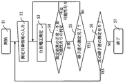
図5は、本発明の実施例1の不良碍子検出装置を用いた不良碍子検出方法の処理手順を示すフローチャートである。
(Defective insulator detection method)
FIG. 5 is a flowchart showing a processing procedure of a defective insulator detecting method using the defective insulator detecting apparatus according to the first embodiment of the present invention.
表示部40に設けられた図示しない電源スイッチを押してバッテリ44により電源を投入すると、装置が初期化された後に起動し、検出動作が開始される(ステップS1)。不良碍子の測定を始める前に、操作部50の設定ボタンを押下して、これから測定を行う碍子の測定対象情報を入力する(ステップS2)。測定対象である碍子連1におけるアース側の碍子1aの両端に第1及び第2のホーン13−1,13−2を接触させ、分担電圧を測定する(ステップS3)。測定された分担電圧は、パルス発振部20内の分担電圧整流部21で直流電圧に整流され、パルス発振部22で分担電圧に応じたパルス信号に変換された後、スピーカ23により音響パルス信号に変換され、絶縁中空パイプ10の先端部10aから後端部10bへ送出される。
When a power switch (not shown) provided on the
絶縁中空パイプ10の後端部10bへ送出された音響パルス信号は、マイクロホン25で電気的なパルス信号に変換され、フィルタ31及びアンプ32により最適な音声波形に変換された後、マルチバイブレータ33により一定の方形波のパルス信号に変換されて、表示部40内のマイコン41へ送られる。マイコン41は、マルチバイブレータ33から送られてきたパルス信号のパルス間隔を測定することにより、デジタル的に分担電圧を計測し、計測した分担電圧値が適正か否かを判断し、表示部本体42による表示と音によって作業者に通知する(ステップS4)。例えば、分担電圧の計測時、2枚目以降の碍子に対して、前回計測した分担電圧値に対して所定の範囲内に入っている場合を正常、入っていない場合を不良可能性有りとみなす。計測されたデータは、マイコン41内のデータメモリ41bに自動的に保存され、報告書の作成を支援する。
The acoustic pulse signal sent to the
図5の碍子分担電圧の測定結果の例が図6に示されている。この図6には、例えば、碍子連位置情報が「内側」、相別情報が「下相」、起点・終点情報が「若番」の碍子の測定結果が示されている。 An example of the measurement result of the insulator sharing voltage in FIG. 5 is shown in FIG. FIG. 6 shows, for example, the measurement results of the insulators whose insulator continuous position information is “inside”, the phase-specific information is “lower phase”, and the start / end point information is “young”.
ステップS4における測定結果が不良可能性有りの場合は、ステップS3へ戻り、再度測定を行う等、測定ミスがないようにする。測定結果が正常の場合は、碍子連1の測定を完了したか否かを判定し(ステップS5)、測定を完了していない場合は、ステップS3へ戻り、アース側からライン側に向かって碍子連数分同様の操作を行う。ステップS5において、碍子連1の測定が完了したと判定された場合は、次の碍子連の測定が有るか否かが判定される(ステップS6)。次の碍子連の測定が有る場合は、ステップS2へ戻り、前記と同様の処理を繰り返す。次の碍子連の測定が無い場合には、不良碍子検出処理を終了する(ステップS7)。
If there is a possibility that the measurement result in step S4 is defective, the process returns to step S3 so that there is no measurement error such as performing measurement again. If the measurement result is normal, it is determined whether or not the measurement of the
(実施例1の効果)
本実施例1の不良碍子検出方法及び不良碍子検出装置によれば、次の(a)〜(c)のような効果がある。
(Effect of Example 1)
According to the defective insulator detecting method and the defective insulator detecting apparatus of the first embodiment, there are the following effects (a) to (c).
(a) 第1、第2のホーン13−1,13−2の近傍に取り付けられた第1、第2のサブホーン14−1,14−2を用い、第1及び第2のホーン13−1,13−2間に生じる計測手順上不要な電位差をキャンセルするようにしたので、静電誘導による誤動作を防止できる。その結果、デジタル信号処理等による自動化によって作業性の向上を図ることができ、測定時の人員削減、測定時間の大幅な短縮、測定後の作業の簡素化が可能になり、送電保守作業等の効率向上と経費削減が期待できる。 (A) First and second horns 13-1 are used by using first and second subhorns 14-1 and 14-2 attached in the vicinity of the first and second horns 13-1 and 13-2. , 13-2, the potential difference unnecessary for the measurement procedure is canceled, so that malfunction due to electrostatic induction can be prevented. As a result, it is possible to improve workability by automation using digital signal processing, etc., and it is possible to reduce personnel during measurement, greatly reduce measurement time, simplify work after measurement, such as power transmission maintenance work Efficiency improvement and cost reduction can be expected.
(b) 操作部50から測定開始の操作指示がマイコン41に入力されると、プログラムメモリ41aに記憶された制御プログラムに従い、計測対象である碍子の枚数分に応じた測定回数だけ測定処理が自動的に行われる構成にしたので、測定開始の操作を行って一旦測定が開始されると、その後は、所定の測定回数(測定対象である碍子の枚数分に応じた測定回数)を終える迄の間、手動の操作が一切不要になる。そのため、作業員は、制御プログラムの測定処理に応じて発生する合図等に従って、測定対象の碍子に順次第1及び第2のホーン13−1,13−2を接触させて測定しさえすれば良いので、測定作業が簡単になる。
(B) When an operation instruction for starting measurement is input from the
(c) 従来、例えば、測定した測定値に関しては、対象の碍子を測定している際に表示部に表示される測定値を確認して測定値を記録帳等に記録し、記録を終えた後、次の測定対象の碍子の測定に移行し、この作業を繰り返さなければならないという不利不便さがあった。即ち、測定作業は例えば上空の鉄塔(足場の不安定な危険が伴う場所)等で行われることから、極力簡素であることが望まれるが、従来の測定方式では作業性が悪く、作業人員も複数名必要であるという不利不便さがあった。これに対し、本実施例1では、測定された測定値については測定時にマイコン41内のデータメモリ41bに自動的に記憶されるようになっており、一連の全ての碍子を測定し終えた後に、都合の良い時に、操作部50を操作することにより、表示部本体42で確認が可能となっている。そのため、作業性が良く、作業人員が1名でも作業が可能である。
(C) Conventionally, for example, with respect to the measured value measured, the measured value displayed on the display unit when the target insulator was measured was recorded, and the measured value was recorded in a record book or the like, and the recording was completed. Later, there was an inconvenience that it was necessary to move to the measurement of the next insulator to be measured and to repeat this operation. That is, since the measurement work is performed, for example, in an empty steel tower (a place where the danger of unstable scaffolding) is desired, it is desirable that the measurement work be as simple as possible. There was the disadvantage that multiple people were needed. On the other hand, in the first embodiment, the measured values are automatically stored in the data memory 41b in the
1 碍子連
1a,1b,1c 碍子
10 絶縁中空パイプ
13−1,13−2 第1、第2のホーン
14−1,14−2 第1、第2のサブホーン
18 絶縁カバー
20 パルス発振部
25 マイクロホン
30 信号処理部
40 表示部
41 マイコン
42 表示部本体
50 操作部
1
Claims (8)
前記第1の処理で測定された前記電位差を、その大きさに応じた周期的なパルス信号に変換して送信する第2の処理と、
前記送信箇所から所定距離離れた位置において前記パルス信号を受信して前記パルス信号の信号周期を検出し、前記検出した信号周期に基づいて前記電位差に対応する分担電圧を算出する第3の処理と、
前記第3の処理で算出された前記分担電圧から、前記分担電圧の適正を判断し判断結果を出力する第4の処理と、
を有することを特徴とする不良碍子検出方法。 Using a first horn, a second horn, and a sub horn attached in the vicinity of the first or second horn, the first and second horns are brought into contact with both ends of an insulator to be measured. A first process of measuring a potential difference between both ends of the insulator by canceling a potential difference unnecessary for measurement generated between the first and second horns with the sub horn;
A second process for converting the potential difference measured in the first process into a periodic pulse signal corresponding to the magnitude and transmitting the pulse signal;
A third process of receiving the pulse signal at a position away from the transmission location by a predetermined distance, detecting a signal period of the pulse signal, and calculating a shared voltage corresponding to the potential difference based on the detected signal period; ,
A fourth process for determining the appropriateness of the shared voltage from the shared voltage calculated in the third process and outputting a determination result;
A defective insulator detecting method characterized by comprising:
測定開始の操作指示が入力されると、予め記憶された制御プログラムに従い、前記計測対象である碍子の分担電圧を自動的に測定し、所定の枚数分だけ測定を繰り返すことを特徴とする請求項2記載の不良碍子検出方法。 The second, third and fourth processes are:
2. When a measurement start operation instruction is input, according to a control program stored in advance, the shared voltage of the insulator to be measured is automatically measured, and the measurement is repeated for a predetermined number of sheets. 2. The defective insulator detecting method according to 2.
データ出力のための操作指示が入力されると、前記制御プログラムに従い、前記データ記憶部の記憶内容が読み出されて出力されることを特徴とする請求項3記載の不良碍子検出方法。 The shared voltage calculation result in the third process is automatically stored in the data storage unit according to the control program,
4. The defective insulator detecting method according to claim 3, wherein when an operation instruction for data output is input, the stored contents of the data storage unit are read and output according to the control program.
前記伝送媒体の一方の端部に装着され、計測対象である碍子の両端に接触させて前記碍子の両端の電位差を測定するための第1及び第2のホーンと、
前記第1又は第2のホーンの近傍において、前記第1又は第2のホーンの軸方向に対して略平行に並設され、且つ前記第1又は第2のホーンと電気的に接続され、前記測定された電位差に対し、前記第1及び第2のホーン間に生じる計測手順上不要な電位差をキャンセルするためのサブホーンと、
前記伝送媒体の一方の端部側に取り付けられ、前記測定された電位差の大きさに応じた周期的なパルス信号に変換して前記伝送媒体へ送出するパルス発振部と、
前記伝送媒体の他方の端部側に取り付けられ、前記伝送媒体から伝送されてくる前記パルス信号を受信して前記パルス信号の信号周期を検出し、前記検出した信号周期に基づいて前記測定された電位差に対応する分担電圧を算出し、前記算出された分担電圧から前記分担電圧の適正を判断し判断結果を出力する信号処理出力部と、
を有することを特徴とする不良碍子検出装置。 A transmission medium having a predetermined length made of an insulating member for transmitting a pulse signal;
First and second horns mounted on one end of the transmission medium, for measuring a potential difference between both ends of the insulator in contact with both ends of the insulator to be measured;
In the vicinity of the first or second horn, it is juxtaposed in parallel with the axial direction of the first or second horn, and is electrically connected to the first or second horn, A sub horn for canceling a potential difference unnecessary for the measurement procedure generated between the first and second horns with respect to the measured potential difference;
A pulse oscillating unit that is attached to one end side of the transmission medium, converts it into a periodic pulse signal corresponding to the measured potential difference, and sends it to the transmission medium;
It is attached to the other end of the transmission medium, receives the pulse signal transmitted from the transmission medium, detects the signal period of the pulse signal, and measures the measurement based on the detected signal period A signal processing output unit that calculates a shared voltage corresponding to the potential difference, determines the appropriateness of the shared voltage from the calculated shared voltage, and outputs a determination result;
A defective insulator detecting device comprising:
前記サブホーンの全体と前記サブホーンに並設される前記第1又は第2のホーンの一部とを被覆すると共に、前記サブホーンと前記第1又は第2のホーンとの間を電気的に絶縁するための絶縁カバーを有することを特徴とする不良碍子検出装置。 The defective insulator detecting device according to claim 6 further includes:
Covering the whole of the sub horn and a part of the first or second horn arranged in parallel to the sub horn, and electrically insulating the sub horn and the first or second horn. A defective insulator detecting device comprising an insulating cover.
前記信号処理出力部は、
前記絶縁中空パイプの他方の端部に内蔵され、前記絶縁中空パイプから伝送されてくる前記音響パルス信号を受信して電気的なパルス信号に変換するパルス受信部と、
前記絶縁中空パイプの他方の端部に内蔵され、前記電気的なパルス信号の信号周期を検出し、前記検出した信号周期に基づいて前記測定された電位差に対応する分担電圧を算出する信号処理部と、
前記絶縁中空パイプの外周面に装着され、前記算出された分担電圧を表示すると共に、前記算出された分担電圧から前記分担電圧の適正を判断し判断結果を表示する表示部と、
前記絶縁中空パイプの外周面に装着され、少なくとも、前記分担電圧の測定開始及び測定対象情報を設定するための操作部と、
を有することを特徴とする請求項6又は7記載の不良碍子検出装置。 The pulse oscillation unit is built in one end of the insulating hollow pipe and is electrically connected to the first and second horns, and when the voltage between the first and second horns is generated, Driven by the inter-horn voltage, is configured to oscillate a periodic acoustic pulse signal according to the magnitude of the inter-horn voltage,
The signal processing output unit
A pulse receiving unit built in the other end of the insulated hollow pipe, receiving the acoustic pulse signal transmitted from the insulated hollow pipe and converting it into an electrical pulse signal;
A signal processing unit that is built in the other end of the insulated hollow pipe, detects a signal period of the electrical pulse signal, and calculates a shared voltage corresponding to the measured potential difference based on the detected signal period When,
A display unit that is mounted on the outer peripheral surface of the insulated hollow pipe, displays the calculated shared voltage, displays a determination result by determining the appropriateness of the shared voltage from the calculated shared voltage, and
An operation unit mounted on the outer peripheral surface of the insulated hollow pipe, at least for setting the measurement start and measurement target information of the shared voltage;
The defective insulator detecting apparatus according to claim 6 or 7, characterized by comprising:
Priority Applications (1)
| Application Number | Priority Date | Filing Date | Title |
|---|---|---|---|
| JP2007236120A JP2009070638A (en) | 2007-09-12 | 2007-09-12 | Faulty insulator detecting method and its device |
Applications Claiming Priority (1)
| Application Number | Priority Date | Filing Date | Title |
|---|---|---|---|
| JP2007236120A JP2009070638A (en) | 2007-09-12 | 2007-09-12 | Faulty insulator detecting method and its device |
Publications (1)
| Publication Number | Publication Date |
|---|---|
| JP2009070638A true JP2009070638A (en) | 2009-04-02 |
Family
ID=40606687
Family Applications (1)
| Application Number | Title | Priority Date | Filing Date |
|---|---|---|---|
| JP2007236120A Pending JP2009070638A (en) | 2007-09-12 | 2007-09-12 | Faulty insulator detecting method and its device |
Country Status (1)
| Country | Link |
|---|---|
| JP (1) | JP2009070638A (en) |
Cited By (3)
| Publication number | Priority date | Publication date | Assignee | Title |
|---|---|---|---|---|
| CN102866314A (en) * | 2012-09-10 | 2013-01-09 | 山东电力集团公司聊城供电公司 | Method for online detecting unfavorable insulator of power transmission circuit |
| KR101242477B1 (en) | 2012-09-24 | 2013-03-12 | 주식회사 금화전기 | Apparatus detecting energized insulator polymer for distribution line |
| CN107588866A (en) * | 2017-10-18 | 2018-01-16 | 广东电网有限责任公司电力科学研究院 | A kind of GIS disc insulators system for detecting temperature |
Citations (13)
| Publication number | Priority date | Publication date | Assignee | Title |
|---|---|---|---|---|
| JPS57194365A (en) * | 1981-05-26 | 1982-11-29 | Sumitomo Electric Ind Ltd | Detector for defective insulator |
| JPS58120175A (en) * | 1982-01-12 | 1983-07-16 | Fuji Electric Corp Res & Dev Ltd | Arc voltage measuring apparatus |
| JPS60262071A (en) * | 1984-06-08 | 1985-12-25 | Sumitomo Electric Ind Ltd | Share voltage measuring apparatus for ceramic insulator |
| JPH02139811A (en) * | 1988-11-18 | 1990-05-29 | Ngk Insulators Ltd | Defective insulator sensor |
| JPH02158016A (en) * | 1988-12-08 | 1990-06-18 | Ngk Insulators Ltd | Poor insulator detector |
| JPH02192625A (en) * | 1989-01-20 | 1990-07-30 | Ngk Insulators Ltd | Method for detecting defective insulator |
| JPH03176670A (en) * | 1989-12-05 | 1991-07-31 | Sankooshiya:Kk | Voltage-pulse converter and voltage measuring device using the same |
| JPH04249012A (en) * | 1991-01-31 | 1992-09-04 | Ngk Insulators Ltd | Defective insulator detector |
| JPH05264644A (en) * | 1992-03-19 | 1993-10-12 | Ngk Insulators Ltd | Failure detecting device for insulator |
| JPH05281286A (en) * | 1992-03-31 | 1993-10-29 | Ngk Insulators Ltd | Device for detecting failure of insulator |
| JPH065045U (en) * | 1992-06-24 | 1994-01-21 | 日本碍子株式会社 | Defective insulator detector |
| JPH06138170A (en) * | 1992-10-29 | 1994-05-20 | Kansai Electric Power Co Inc:The | Fault detector for lightening insulator |
| JP2006196382A (en) * | 2005-01-17 | 2006-07-27 | Ngk Insulators Ltd | Faulty insulator detector |
-
2007
- 2007-09-12 JP JP2007236120A patent/JP2009070638A/en active Pending
Patent Citations (13)
| Publication number | Priority date | Publication date | Assignee | Title |
|---|---|---|---|---|
| JPS57194365A (en) * | 1981-05-26 | 1982-11-29 | Sumitomo Electric Ind Ltd | Detector for defective insulator |
| JPS58120175A (en) * | 1982-01-12 | 1983-07-16 | Fuji Electric Corp Res & Dev Ltd | Arc voltage measuring apparatus |
| JPS60262071A (en) * | 1984-06-08 | 1985-12-25 | Sumitomo Electric Ind Ltd | Share voltage measuring apparatus for ceramic insulator |
| JPH02139811A (en) * | 1988-11-18 | 1990-05-29 | Ngk Insulators Ltd | Defective insulator sensor |
| JPH02158016A (en) * | 1988-12-08 | 1990-06-18 | Ngk Insulators Ltd | Poor insulator detector |
| JPH02192625A (en) * | 1989-01-20 | 1990-07-30 | Ngk Insulators Ltd | Method for detecting defective insulator |
| JPH03176670A (en) * | 1989-12-05 | 1991-07-31 | Sankooshiya:Kk | Voltage-pulse converter and voltage measuring device using the same |
| JPH04249012A (en) * | 1991-01-31 | 1992-09-04 | Ngk Insulators Ltd | Defective insulator detector |
| JPH05264644A (en) * | 1992-03-19 | 1993-10-12 | Ngk Insulators Ltd | Failure detecting device for insulator |
| JPH05281286A (en) * | 1992-03-31 | 1993-10-29 | Ngk Insulators Ltd | Device for detecting failure of insulator |
| JPH065045U (en) * | 1992-06-24 | 1994-01-21 | 日本碍子株式会社 | Defective insulator detector |
| JPH06138170A (en) * | 1992-10-29 | 1994-05-20 | Kansai Electric Power Co Inc:The | Fault detector for lightening insulator |
| JP2006196382A (en) * | 2005-01-17 | 2006-07-27 | Ngk Insulators Ltd | Faulty insulator detector |
Cited By (4)
| Publication number | Priority date | Publication date | Assignee | Title |
|---|---|---|---|---|
| CN102866314A (en) * | 2012-09-10 | 2013-01-09 | 山东电力集团公司聊城供电公司 | Method for online detecting unfavorable insulator of power transmission circuit |
| KR101242477B1 (en) | 2012-09-24 | 2013-03-12 | 주식회사 금화전기 | Apparatus detecting energized insulator polymer for distribution line |
| CN107588866A (en) * | 2017-10-18 | 2018-01-16 | 广东电网有限责任公司电力科学研究院 | A kind of GIS disc insulators system for detecting temperature |
| CN107588866B (en) * | 2017-10-18 | 2023-05-23 | 广东电网有限责任公司电力科学研究院 | GIS basin-type insulator temperature detection system |
Similar Documents
| Publication | Publication Date | Title |
|---|---|---|
| KR101070329B1 (en) | Portable ultrasonic partial discharge measurement device having ccd camera, and partial discharge measurement method using the same | |
| KR101275097B1 (en) | Inspect apparatus and method system of on-line non destructive testing for spot welding | |
| JP2007292489A (en) | Insulation abnormality diagnosis system of electric facilities | |
| JP4869091B2 (en) | Insulation abnormality diagnosis system for electrical equipment | |
| JP2009070638A (en) | Faulty insulator detecting method and its device | |
| JP2010190626A (en) | Device and method for diagnosis of partial discharge deterioration | |
| KR102003966B1 (en) | Sensing apparatus for monitoring real-time fault diagnosis of self-generating high pressure transmission dc cable, monitoring system and method for the same | |
| JP2006515063A (en) | DCVG-CIPS measuring device for detecting results about pipelines | |
| KR101410741B1 (en) | Portable ultrasonic partial discharge measurement device and method which can guide fault position | |
| JP2007263845A (en) | Flow rate measuring device and method | |
| JP2006304523A (en) | Management system of power distribution facility and management method of power distribution facility | |
| JP4398198B2 (en) | Insulation degradation region diagnosis system and method for electric wire or cable | |
| US10876940B2 (en) | Material testing machine with a control device for cable disconnection warning | |
| KR20090123478A (en) | Apparatus and system for inspecting insulator | |
| KR101157189B1 (en) | Portable Direct Current Ground Detecting Apparatus and Detecting Method using the same | |
| CN113720508A (en) | Pillar porcelain insulator stress monitoring device and method based on double laser scanning | |
| US11788879B2 (en) | State analysis of an inductive operating resource | |
| EP2910963B1 (en) | Methods and instruments for testing batteries | |
| KR101527942B1 (en) | Device For Measuring A Distance About Grounding Point Of The Control Cable In Railway Substation And Method Therefore | |
| CN112461371A (en) | Portable thermal imager system with laser range finder | |
| JP2015102375A (en) | Ground resistance meter | |
| JP5661025B2 (en) | In-tube ultrasonic flaw detector | |
| JP2010164544A (en) | Comparison measurement instrument for change in physical value | |
| JP2007127462A (en) | Insulation level monitoring device | |
| JP2921778B2 (en) | Data transmission method near high-voltage charging section and abnormal approach warning system to high-voltage charging section |
Legal Events
| Date | Code | Title | Description |
|---|---|---|---|
| A711 | Notification of change in applicant |
Effective date: 20100609 Free format text: JAPANESE INTERMEDIATE CODE: A711 |
|
| A521 | Written amendment |
Free format text: JAPANESE INTERMEDIATE CODE: A821 Effective date: 20100609 |
|
| A621 | Written request for application examination |
Free format text: JAPANESE INTERMEDIATE CODE: A621 Effective date: 20100823 |
|
| A977 | Report on retrieval |
Effective date: 20120928 Free format text: JAPANESE INTERMEDIATE CODE: A971007 |
|
| A131 | Notification of reasons for refusal |
Free format text: JAPANESE INTERMEDIATE CODE: A131 Effective date: 20121218 |
|
| A02 | Decision of refusal |
Free format text: JAPANESE INTERMEDIATE CODE: A02 Effective date: 20130604 |