JP2009058564A - Electro-optical device manufacturing apparatus and method - Google Patents
Electro-optical device manufacturing apparatus and method Download PDFInfo
- Publication number
- JP2009058564A JP2009058564A JP2007223546A JP2007223546A JP2009058564A JP 2009058564 A JP2009058564 A JP 2009058564A JP 2007223546 A JP2007223546 A JP 2007223546A JP 2007223546 A JP2007223546 A JP 2007223546A JP 2009058564 A JP2009058564 A JP 2009058564A
- Authority
- JP
- Japan
- Prior art keywords
- substrate
- glass substrate
- pressure
- liquid crystal
- electro
- Prior art date
- Legal status (The legal status is an assumption and is not a legal conclusion. Google has not performed a legal analysis and makes no representation as to the accuracy of the status listed.)
- Withdrawn
Links
- 238000000034 method Methods 0.000 title claims description 26
- 238000004519 manufacturing process Methods 0.000 title claims description 15
- 239000000758 substrate Substances 0.000 claims abstract description 253
- 239000011521 glass Substances 0.000 claims abstract description 86
- 238000003825 pressing Methods 0.000 claims abstract description 47
- 238000002788 crimping Methods 0.000 claims description 19
- 239000000463 material Substances 0.000 claims description 13
- 239000004973 liquid crystal related substance Substances 0.000 abstract description 51
- 239000000853 adhesive Substances 0.000 description 14
- 230000001070 adhesive effect Effects 0.000 description 14
- 239000000428 dust Substances 0.000 description 8
- 239000010408 film Substances 0.000 description 7
- 238000007789 sealing Methods 0.000 description 7
- 238000005452 bending Methods 0.000 description 4
- 238000010586 diagram Methods 0.000 description 3
- 238000002347 injection Methods 0.000 description 3
- 239000007924 injection Substances 0.000 description 3
- 239000011159 matrix material Substances 0.000 description 3
- 230000002093 peripheral effect Effects 0.000 description 3
- 229920001187 thermosetting polymer Polymers 0.000 description 3
- 230000001771 impaired effect Effects 0.000 description 2
- 239000010409 thin film Substances 0.000 description 2
- XUIMIQQOPSSXEZ-UHFFFAOYSA-N Silicon Chemical compound [Si] XUIMIQQOPSSXEZ-UHFFFAOYSA-N 0.000 description 1
- NIXOWILDQLNWCW-UHFFFAOYSA-N acrylic acid group Chemical group C(C=C)(=O)O NIXOWILDQLNWCW-UHFFFAOYSA-N 0.000 description 1
- -1 and the seal member Substances 0.000 description 1
- 239000003795 chemical substances by application Substances 0.000 description 1
- 238000004140 cleaning Methods 0.000 description 1
- 239000006063 cullet Substances 0.000 description 1
- 230000003287 optical effect Effects 0.000 description 1
- 229920001721 polyimide Polymers 0.000 description 1
- 229910052710 silicon Inorganic materials 0.000 description 1
- 239000010703 silicon Substances 0.000 description 1
Images


Landscapes
- Liquid Crystal (AREA)
Abstract
【課題】液晶パネルの外表面にガラス基板を貼り合わせるに際し、ガラス基板に外力が印加されても液晶分子の配向状態に乱れが生じることが無く、表示品位の高い画像を得ることができるようにする。
【解決手段】TFT基板10が多数枚取り可能に形成されている大型基板110の、各TFT基板10が形成されている領域に対向基板20がシール部材52を介して貼り合わされていると共に、TFT基板10と対向基板20とシール部材52とで囲まれた空隙に液晶50が充填されており、対向基板20の外表面に防塵ガラス基板31を圧着ヘッド47の押圧面47aにて押圧して圧着させるに際し、圧着ヘッド47の押圧面47aにてシール部材52の直上を押圧する。
【選択図】図6When a glass substrate is bonded to the outer surface of a liquid crystal panel, the orientation state of liquid crystal molecules is not disturbed even when an external force is applied to the glass substrate, and an image with high display quality can be obtained. To do.
A counter substrate is bonded to a region where each TFT substrate is formed on a large substrate on which a large number of TFT substrates are formed so as to be able to take a large number of TFT substrates. A liquid crystal 50 is filled in a space surrounded by the substrate 10, the counter substrate 20, and the seal member 52, and the dust-proof glass substrate 31 is pressed against the outer surface of the counter substrate 20 by the pressing surface 47 a of the pressure-bonding head 47. When doing so, the pressure surface 47 a of the pressure-bonding head 47 is pressed directly above the seal member 52.
[Selection] Figure 6
Description
本発明は、大型基板に貼り合わされている第2の基板の外表面に、ガラス基板を貼り合わせる電気光学装置の製造装置、及び製造方法に関する。 The present invention relates to an electro-optical device manufacturing apparatus and a manufacturing method in which a glass substrate is bonded to the outer surface of a second substrate bonded to a large substrate.
従来、電気光学装置の代表である投射型表示装置では、表示パネルの表面付近に塵埃等が付着すると、それが投射レンズ等により拡大されてスクリーン上に投射され、表示品質を著しく低下させてしまうことになる。これを防止する技術として、例えば特許文献1(特開2003−140125号公報)に開示されているように、表示パネルの外表面に防塵機能を有する透明なガラス基板を貼付する技術が多く採用されている。 Conventionally, in a projection type display device that is representative of an electro-optical device, if dust or the like adheres to the vicinity of the surface of the display panel, it is enlarged by a projection lens or the like and projected onto a screen, thereby significantly reducing display quality. It will be. As a technique for preventing this, for example, as disclosed in Patent Document 1 (Japanese Patent Laid-Open No. 2003-140125), a technique of sticking a transparent glass substrate having a dustproof function to the outer surface of the display panel is often employed. ing.
表示パネルの外表面をガラス基板で保護することで、表示パネル面に対する塵埃等の付着が防止できる。更に、ガラス基板外表面に塵埃等が付着しても、この塵埃等と液晶等の電気光学物質との間の距離がガラス基板の厚み分だけ長くなり、塵埃等の像がデフォーカスされ、スクリーン上に大きくぼやけて表示されるので目立たなくなる。 By protecting the outer surface of the display panel with a glass substrate, dust and the like can be prevented from adhering to the display panel surface. Furthermore, even if dust or the like adheres to the outer surface of the glass substrate, the distance between the dust and the electro-optical material such as liquid crystal is increased by the thickness of the glass substrate, and the image of dust and the like is defocused, and the screen Since it is displayed with a large blur on the top, it becomes inconspicuous.
このガラス基板を表示パネル表面に貼り合わせるに際しては、例えば特許文献2(特開2006−11353号公報)開示されているように、テーブルにセットされている基板の表面に接着剤を点描した後、この基板に対し上方から、圧着ヘッドの下端面に吸着されているガラス基板を当接させ、所定に加圧してガラス基板を基板上に圧着する技術が多く採用されている。
ところで、表示パネルの代表である液晶パネルは、画素電極、TFT(Thin Film Transistor)素子、複数の走査線(ゲート線)、複数の信号線(ソース線)及びドライバICなどが形成、若しくは実装されている素子基板と、対向電極などが形成されている対向基板とが枠状のシール部材を介して貼り合わされ、両基板間に電気光学物質としての液晶が充填されている。ガラス基板は、TFT基板と対向基板との両外表面に貼り合わされる。 By the way, a liquid crystal panel, which is a representative display panel, has a pixel electrode, a TFT (Thin Film Transistor) element, a plurality of scanning lines (gate lines), a plurality of signal lines (source lines), a driver IC, and the like formed or mounted. The element substrate and the counter substrate on which the counter electrode and the like are formed are bonded to each other through a frame-shaped seal member, and liquid crystal as an electro-optical material is filled between both the substrates. The glass substrate is bonded to both outer surfaces of the TFT substrate and the counter substrate.
図8、図9には、液晶パネルの製造過程(いわゆる前工程)において、大型基板からチップ状に切り出された対向基板20上にガラス基板31を貼り合わせる工程が示されている。ステージ200上には、多数のTFT基板が形成されている大型基板110が所定に位置決めされた状態で載置固定されており、この各TFT基板の領域に枠状のシール部材52を介して対向基板20が貼り合わされている。液晶は両基板20,110とシール部材52とで囲まれた空隙に滴下注入法(ODF:One Drop Filling)により注入されており、この状態では、前工程が既に完了しているので、液晶の配向状態も調整済みである。
8 and 9 show a process of bonding a
この対向基板20の外表面にガラス基板31を貼り合わせるに際しては、先ず、対向基板20の外表面に透明接着剤を点描し、その後、上方からガラス基板31を圧着させる。ガラス基板31は圧着ヘッド210からの押圧力により圧着される。この圧着ヘッド210のり下端縁に、ガラス基板31を吸着する押圧面210aが形成されており、その内側に吸引凹部210bが形成され、この吸引凹部210bに、吸引通路210cを介して吸引圧が導入されている。従って、ガラス基板31は吸引凹部210bに導入される吸引圧により、押圧面210aに吸着される。
When the
このガラス基板31を対向基板20の表面に貼り合わせるに際しては、対向基板20上に点描されている透明接着剤を、気泡を混入させることなく押し広げる必要がある。又、完成される液晶パネルの画像表示領域のサイズは、用途に応じて様々な大きさを有しており、圧着ヘッド210の大きさは、全ての機種に共用できるように最小の液晶パネルサイズに合わせて設定されている。
When the
そのため、比較的大きなサイズの液晶パネルでは、圧着ヘッド210の大きさが相対的に小さくなり、図8の矢印aで示すように、対向基板20の中心付近に圧着力が集中することになる。その結果、ガラス基板31を介して対向基板20の中央付近が押圧される。対向基板20は、その外縁がシール部材52に支持され、中央付近の大型基板110との間には液晶が充填されているため、圧着ヘッド210から押圧力により対向基板20に曲げ応力が発生し易く、この曲げ応力により中央付近が湾曲されると、液晶分子が押圧される。
Therefore, in a relatively large size liquid crystal panel, the size of the pressure bonding
押圧された液晶分子は移動するため、その部分の配向状態に乱れが生じる。液晶配向の乱れは、圧着ヘッド210による対向基板20への荷重が開放されても、その一部が残ることがあり、画像の表示品位を著しく低下させる原因となる。
Since the pressed liquid crystal molecules move, the alignment state of the portion is disturbed. Even if the load applied to the
又、比較的大きなサイズの液晶パネルでは、圧着ヘッド210の押圧面210aが液晶パネルの画像表示領域上に吸着されるため、この押圧面210aの押圧力により、ガラス基板31の表面が傷付けられてしまう可能性がある。
Further, in a relatively large size liquid crystal panel, the pressing surface 210a of the
本発明は、上記事情に鑑み、表示パネルの外表面にガラス基板を貼り合わせる際に、この表示パネルに外力が印加されても、画像表示領域上のガラス基板が傷つくことが無いばかりか、電気光学物質の配向状態に乱れが生じることが無く、表示品位の高い画像を得ることのできる電気光学装置の製造装置、及び製造方法を提供することを目的とする。 In view of the above circumstances, the present invention does not only damage the glass substrate on the image display area even if an external force is applied to the display panel when the glass substrate is bonded to the outer surface of the display panel. An object of the present invention is to provide an electro-optical device manufacturing apparatus and a manufacturing method capable of obtaining an image with high display quality without causing any disturbance in the alignment state of the optical material.
上記目的を達成するため第1発明は、第1の基板が多数枚取り可能に形成されている大型基板の、該各第1の基板が形成されている領域に第2の基板がシール部材を介して貼り合わされていると共に、前記第1の基板と前記第2の基板と前記シール部材とで囲まれた空隙に電気光学物質が充填されており、前記第2の基板の外表面にガラス基板を圧着ヘッドの押圧面にて押圧して圧着させる電気光学装置の製造装置において、前記圧着ヘッドの前記押圧面が前記シール部材の直上に配設されることを特徴とする。 In order to achieve the above object, according to a first aspect of the present invention, a second substrate has a sealing member in a region where each first substrate is formed in a large substrate on which a large number of first substrates are formed. And a gap surrounded by the first substrate, the second substrate, and the sealing member is filled with an electro-optical material, and an outer surface of the second substrate is a glass substrate. In the electro-optical device manufacturing apparatus in which the pressure is pressed by the pressing surface of the pressure-bonding head, the pressure surface of the pressure-bonding head is disposed immediately above the seal member.
このような構成では、圧着ヘッドのガラス基板を第2の基板方向へ押圧する押圧面が、シール部材の直上に配設されているので、圧着ヘッドからの押圧力が第2の基板に印加されても、この第2の基板に曲げ応力が作用せず、この第2の基板が湾曲することがない。そのため、電気光学物質に外力が印加されず、従って、この電気光学物質の配向状態に乱れが生じることが無く、表示品位の高い画像を得ることができる。 In such a configuration, the pressing surface that presses the glass substrate of the crimping head in the second substrate direction is disposed immediately above the seal member, so that the pressing force from the crimping head is applied to the second substrate. However, bending stress does not act on the second substrate, and the second substrate is not curved. For this reason, no external force is applied to the electro-optical material, so that the orientation state of the electro-optical material is not disturbed, and an image with high display quality can be obtained.
第2発明は、第1発明において、前記圧着ヘッドの前記押圧面が前記シール部材と略同一形状に形成されていることを特徴とする。 A second invention is characterized in that, in the first invention, the pressing surface of the crimping head is formed in substantially the same shape as the sealing member.
このような構成では、圧着ヘッドの押圧面がシール部材と略同一形状に形成されているので、ガラス基板を均一な押圧力で圧着させることができる。 In such a configuration, the pressing surface of the crimping head is formed in substantially the same shape as the sealing member, so that the glass substrate can be crimped with a uniform pressing force.
第3発明は、第1或いは第2発明において、前記圧着ヘッドの前記押圧面の内側に凹部が形成されていることを特徴とする。 According to a third invention, in the first or second invention, a recess is formed inside the pressing surface of the crimping head.
このような構成では、圧着ヘッドの押圧面の内側に凹部が形成されているので、この凹部内に露呈するガラス基板に異物が付着されていても、この異物にてガラス基板が傷付けられることがない。 In such a configuration, since the concave portion is formed inside the pressing surface of the crimping head, even if foreign matter is adhered to the glass substrate exposed in the concave portion, the glass substrate may be damaged by the foreign matter. Absent.
第4発明は、第3発明において、前記凹部が、前記ガラス基板を該押圧面に吸着させる吸引圧を導入する吸引凹部であることを特徴とする。 A fourth invention is characterized in that, in the third invention, the recess is a suction recess for introducing a suction pressure for adsorbing the glass substrate to the pressing surface.
このような構成では、圧着ヘッドの押圧面の内側に形成された凹部を、ガラス基板を押圧面に吸着させる吸引圧を導入する吸引凹部としたので、ガラス基板を押圧面に対して確実に吸着させることができる。 In such a configuration, the recess formed inside the pressing surface of the crimping head is a suction recess that introduces a suction pressure that causes the glass substrate to be attracted to the pressing surface, so that the glass substrate is reliably attracted to the pressing surface. Can be made.
第5発明は、第1の基板が多数枚取り可能に形成されている大型基板の、該各第1の基板が形成されている領域に第2の基板がシール部材を介して貼り合わされていると共に、前記第1の基板と前記第2の基板と前記シール部材とで囲まれた空隙に電気光学物質が充填されており、前記第2の基板の外表面にガラス基板を圧着ヘッドの押圧面にて押圧して圧着させる電気光学装置の製造方法において、前記圧着ヘッドの前記押圧面にて、前記シール部材の直上に位置する前記ガラス基板を前記第2の基板方向へ押圧して圧着させることを特徴とする。 According to a fifth aspect of the present invention, a second substrate is bonded to a region where each first substrate is formed on a large substrate on which a large number of first substrates can be taken. In addition, an electro-optical material is filled in a space surrounded by the first substrate, the second substrate, and the seal member, and a glass substrate is pressed on the outer surface of the second substrate. In the method of manufacturing an electro-optical device that is pressed and pressure-bonded, the glass substrate positioned immediately above the seal member is pressed and pressed toward the second substrate on the pressing surface of the pressure-bonding head. It is characterized by.
このような構成では、圧着ヘッドの押圧面にて、シール部材の直上に位置するガラス基板を第2の基板方向へ押圧して圧着させるようにしたので、圧着ヘッドからの押圧力が第2の基板に印加されても、この第2の基板に曲げ応力が作用せず、この第2の基板が湾曲することがない。そのため、電気光学物質に外力が印加されず、従って、この電気光学物質の配向状態に乱れが生じることが無く、表示品位の高い画像を得ることができる。 In such a configuration, since the glass substrate located immediately above the seal member is pressed toward the second substrate on the pressing surface of the pressure-bonding head to be pressure-bonded, the pressing force from the pressure-bonding head is the second pressure. Even if it is applied to the substrate, no bending stress acts on the second substrate, and the second substrate does not bend. For this reason, no external force is applied to the electro-optical material, so that the orientation state of the electro-optical material is not disturbed, and an image with high display quality can be obtained.
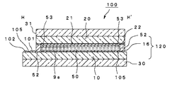
以下、図1〜図7に基づいて本発明の一実施形態を説明する。図1は液晶パネルの平面図、図2はTFT基板と対向基板とを貼り合わせて液晶を封入する組立工程終了後の液晶装置であって、図1のH-H'断面図、図3はTFT基板を多数枚取りできる大型基板に対してチップ状の対向基板が貼り合わされた状態を示す斜視図である。尚、以下においては、薄膜トランジスタ(Thin Film Transistor;TFT)を画素スイッチング素子として備えたアクティブマトリクス型の液晶装置を例に挙げて説明する。 Hereinafter, an embodiment of the present invention will be described with reference to FIGS. 1 is a plan view of a liquid crystal panel, FIG. 2 is a liquid crystal device after the assembly process in which a TFT substrate and a counter substrate are bonded together to enclose liquid crystal, and is a cross-sectional view taken along the line HH ′ of FIG. It is a perspective view which shows the state by which the chip-like counter substrate was bonded together with respect to the large sized substrate which can take many TFT substrates. In the following description, an active matrix liquid crystal device including a thin film transistor (TFT) as a pixel switching element will be described as an example.
先ず、図1、図2を用いて、電気光学装置の一例である、一般的な液晶装置100の全体構成について説明する。液晶装置100は、液晶パネル120と、この液晶パネル120の両外表面に貼り合わされている、防塵機能を有する透明なガラス基板(以下「防塵ガラス基板」と称する)30,31とを備えている。
First, the overall configuration of a general
液晶パネル120は、第1の基板としてのTFT基板10と、これに対向配置される第2の基板としての対向基板20とを有し、両基板10,20の対向面間の画像表示領域10aの周囲に設けたシール領域がシール部材52を介して貼り合わされている。尚、シール部材52の外形と対向基板20の外形とはほぼ同じ大きさに形成されている。
The
更に、この両基板10,20の対向面間とシール部材52とで囲まれた空隙に、電気光学物質である液晶50が滴下注入法(ODF)により充填されている。対向基板20の4隅には、上下導通材106が設けられており、TFT基板10に設けられた上下導通端子107と対向基板20に設けられた対向電極21との間で電気的に導通されている。
Further, a
又、シール部材52が配置されたシール領域の内側に並行して、画像表示領域10aを規定する遮光性の周辺遮光膜53が対向基板20側に設けられている。又、画像表示領域の周辺に広がる周辺領域のうち、シール部材52が配置されたシール領域の外側部分には、データ線駆動回路101及び外部回路接続端子102がTFT基板10の一辺に沿って設けられており、走査線駆動回路104が、この一辺に隣接する2辺に沿って設けられている。
Further, a light-shielding peripheral light-shielding
更に、TFT基板10の残る一辺には、画像表示領域10aの両側に設けられた走査線駆動回路104間を電気的に接続するための複数の配線105が設けられている。尚、走査線駆動回路104、及び配線105は、シール部材52の内側の周辺遮光膜53に対向する位置に配設されている。
Further, on the remaining side of the
更に、TFT基板10上には、後述する画素スイッチング用のTFT素子や走査線、データ線等の配線が形成された後の画素電極9a上に配向膜16が形成されている。他方、対向基板20上には、対向電極(ITO)21の他、最上層部分に配向膜22が形成されており、これら一対の配向膜16,22間で、所定の配向状態が設定される。尚、各配向膜16,22は、ポリイミド膜等の透明な有機膜で構成されている。
Further, on the
液晶パネル120の両外表面に貼り合わされている防塵ガラス基板30,31は、塵埃等が液晶パネル120の表面に付着することを防止すると共に、塵埃等が液晶表示面から離間させてデフォーカスすることで、塵埃等の像を目立たなくさせる機能をも有する。このような機能を実現するために、防塵ガラス基板30,31は、板厚が1〜3mm程度と比較的厚く形成されており、その材質は、TFT基板10や対向基板20と同一のものが使用されている。又、防塵ガラス基板30,31は、液晶パネル120の表面に対し、TFT基板10や対向基板20(及び防塵ガラス基板30,31)と同じ屈折率に調整されたシリコン系接着剤やアクリル系接着剤等からなる熱硬化型或いは紫外線硬化型等の透明接着剤を用いて、両基板10,20の外表面に接着されている。
The dust-
TFT基板10と対向基板20とは、前工程において、それぞれ多数枚取りできる大型基板の状態で製造される。そして、先ず、対向基板20のみが大型基板からチップ状に切り出される。大型基板から切り出された対向基板20は、TFT基板10を多数枚取りできる大型基板110のTFT基板10が形成されている領域に各々貼り合わされる(図3参照)。尚、大型基板110と対向基板20との間には液晶が滴下注入法(ODF)により充填されている。又、1枚の大型基板110から切り出すことのできるチップ状のTFT基板10の枚数は、この大型基板110の大きさ、及び製造する液晶パネルのサイズにより決定される。従って、図3に記載されているTFT基板10の切り出し枚数(12枚)は一例に過ぎない。更に、本実施形態による大型基板110は円板状に形成されているが、形状はこれに限定されるものではなく矩形状であっても良い。
The
又、防塵ガラス基板30を多数枚取りできる大型防塵ガラス基板300は、大型基板110の底面に、この大型基板110とほぼ同一の大きさで実装される。又、他方の防塵ガラス基板31は、大型基板110に貼り合わされている対向基板20上に実装される。
In addition, a large dust-
図4に、大型基板110の外表面と、この大型基板110の上面に貼り合わされている対向基板20の外表面とに防塵ガラス基板300,31をそれぞれ実装する工程を示す。尚、この作業はクリーンルーム内で行われる。
FIG. 4 shows a process of mounting the dust-
工程(a):先ず、大型基板110のTFT基板10が形成されている領域上に対向基板20を所定に位置決めして貼り合わせた後、動作状態等の検査を行う。
Step (a): First, the
工程(b):次いで、各対向基板20の外表面に対向基板20とほぼ同一形状の防塵ガラス基板31を貼り合わせる。
Step (b): Next, a dust-
工程(c):その後、全体を洗浄した後、大型基板110の、対向基板20が貼り合わされている面と反対側の面である外表面に、大型基板110とほぼ同一かやや小さい形状の大型防塵ガラス基板300を貼付する。
Step (c): After cleaning the whole, a large-
工程(d):大型基板110の対向基板20が張り合わされている側の面の、対向基板20間にスクライブラインを形成し、このスクライブラインに沿って大型基板110を分割し、チップ状の液晶装置100を切り出す。このとき大型防塵ガラス基板300も、チップ状の防塵ガラス基板30に切り出される。
Step (d): A scribe line is formed between the opposing
尚、防塵ガラス基板30,31の実装工程においては、工程(b)と工程(c)とを入れ換え、対向基板20に対して防塵ガラス基板31を貼付する前に、大型基板110に大型防塵ガラス基板300を貼付するようにしても良い。
In the mounting process of the
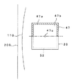
次に、図4(b)に示す防塵ガラス基板(以下、「小型防塵ガラス基板」と称する)31の実装工程について、図5の工程図を参照しながら更に詳しく説明する。尚、小型防塵ガラス基板31の貼り合わせは常圧下で行われる。
Next, the mounting process of the dustproof glass substrate (hereinafter referred to as “small dustproof glass substrate”) 31 shown in FIG. 4B will be described in more detail with reference to the process diagram of FIG. The small dust-
工程(a):先ず、ステージ200上に大型基板110を所定に位置決めした状態で載置固定する。次いで、1つの対向基板20の上面中央に、熱硬化或いは紫外線硬化型の透明接着剤41を滴下する。尚、このステージ200は、所定温度に加熱されているホットプレートであっても良く、この場合、透明接着剤41としては熱硬化型を使用する。
Step (a): First, the
又、この対向基板20の上方に圧着ヘッド47が待機している。この圧着ヘッド47はエアシリンダ(図示せず)等のアクチュエータに着脱自在に支持されており、このアクチュエータの動作により昇降自在にされている。又、圧着ヘッド47と、大型基板110を載置するステージ200とは、水平方向へ相対移動自在にされており、この圧着ヘッド47とステージ200とは、予め記憶されている各対向基板20の位置を示すX−Y座標データに従い、自動的に位置決めされる。
The
この圧着ヘッド47の下端面に、小型防塵ガラス基板31を吸着する押圧面47aが形成されている。図6、図7に示すように、この圧着ヘッド47の押圧面47aは、液晶パネル120(図1、図2参照)の基板10,20間を貼り合わせるシール部材52とほぼ同一形状に形成されている。従って、この圧着ヘッド47は液晶パネル120に形成されるシール部材52の大きさ毎に専用化されている。尚、図7には圧着ヘッド47が上半分の断面で示されている。
A pressing surface 47 a that adsorbs the small
又、圧着ヘッド47の押圧面47aの内側に吸引凹部47bが形成され、この吸引凹部47bが吸引通路47cを介して真空ポンプ(図示せず)に連通されている。小型防塵ガラス基板31が圧着ヘッド47の下端に形成された押圧面47aに、所定に位置決めされた状態で当接されると、真空ポンプ(図示せず)からの吸引圧が吸引通路47cを経て吸引凹部47bに導入され、この吸引凹部47bに発生する吸引圧により、小型防塵ガラス基板31が押圧面47aに吸着される。
Further, a suction recess 47b is formed inside the pressing surface 47a of the crimping
工程(b):圧着ヘッド47を下降させ押圧面47aに吸着されている小型防塵ガラス基板31を、対向基板20の上面に、押圧面47aがシール部材52の直上に位置するように位置合わせした状態で当接させる(図6、図7参照)。そして、この状態で、所定時間(例えば10〜20[sec]程度)、所定圧着力(例えば0.15[Kg/cm2]程度)で押圧し、小型防塵ガラス基板31を対向基板20に圧着させる。
Step (b): The pressure-
すると、透明接着剤41が気泡の混入を阻止しながら周囲へ拡散し、小型防塵ガラス基板31が対向基板20上に圧着される。尚、圧着ヘッド47の圧着時間、圧着力は、透明接着剤41を気泡の混入を阻止しながら全体に拡散させるに要する時間、及び透明接着剤41の硬化に要する時間に応じて設定される。
Then, the
又、図6、図7に示すように、小型防塵ガラス基板31は、その周縁のみが圧着ヘッド47の押圧面47aに吸着されており、圧着ヘッド47に形成されている吸引凹部47bには非接触状態となる。そのため、この吸引凹部47b内に露呈されている小型防塵ガラス基板31の表面、すなわち、液晶パネル120の画像表示領域10a上にカレット(ガラスの切粉)等の異物が付着されていても、小型防塵ガラス基板31の表面が傷つくことはない。その結果、小型防塵ガラス基板31を透過して投射される画像の表示品位が損なわれることがない。
As shown in FIGS. 6 and 7, only the periphery of the small dust-
更に、圧着ヘッド47の押圧面47aがシール部材52の直上に位置しているので、圧着ヘッド47からの押圧力は、図6の矢印aで示すように、そのままシール部材52全体に伝達されることになる。その結果、小型防塵ガラス基板31を介して対向基板20に、この対向基板20を湾曲させるような曲げ応力が作用せず内部に充填されている液晶分子が押圧されることがなく、従って、液晶分子の配向状態に乱れが生じることが無く、表示品位の高い画像を得ることができる。
Further, since the pressing surface 47a of the crimping
工程(c):圧着ヘッド47による小型防塵ガラス基板31の圧着時間が所定圧着時間に達した後、透明接着剤41を硬化させ、その後、圧着ヘッド47を上昇させる。すると、小型防塵ガラス基板31は透明接着剤41により対向基板20に接着されているため、圧着ヘッド47の押圧面47aから離間し、小型防塵ガラス基板31の接着が完了する。
Step (c): After the pressure bonding time of the small dust-
次いで、ステージ200と圧着ヘッド47とを相対移動させて、隣の対向基板20上に圧着ヘッド47を対設させると共に、上述した各工程(a)〜(c)と同一の工程を繰り返して、当該対向基板20に小型防塵ガラス基板31を接着する。これを残りの対向基板20に対して繰り返すことで、大型基板110に貼り合わされている全ての対向基板20の外表面に対して小型防塵ガラス基板31を貼り合わせる。
Next, the
尚、上述した実施形態では、1つの圧着ヘッド47で小型防塵ガラス基板31を1枚ずつ対向基板20に圧着させるシングルヘッド方式について説明したが、本発明は、複数配列の圧着ヘッドを用いて、複数の小型防塵ガラス基板31を同時に圧着させるマルチヘッド方式であっても良い。
In the above-described embodiment, the single head method in which the small dust-
このように、本実施形態によれば、対向基板20の外表面に対して小型防塵ガラス基板31を実装する工程では、この小型防塵ガラス基板31を吸着する圧着ヘッド47の押圧面47aを、シール部材52とほぼ同一形状に形成されているため、圧着ヘッド47からの押圧力が対向基板20に印加されても、対向基板20が湾曲せず、従って、内部に充填されている液晶分子が押圧されることがないので、液晶分子の配向状態に乱れが生じることが無く、表示品位の高い画像を得ることができる。
Thus, according to the present embodiment, in the step of mounting the small
又、押圧面47aの内側、すなわち、液晶パネル120の画像表示領域10a上に位置する部位に吸引凹部47bが形成されているため、吸引凹部47bに混入した異物が小型防塵ガラス基板31に付着しても、この異物により小型防塵ガラス基板31の表面が傷付けられることが無く、投射される画像の表示品位を損なうことがない。
In addition, since the suction recess 47b is formed inside the pressing surface 47a, that is, on the image display region 10a of the
本発明による電気光学装置は、TFTアクティブマトリクス駆動方式の液晶装置に限らず、パッシブマトリックス型の液晶装置、TFD(薄型ダイオード)をスイッチング素子として備えた液晶装置に適用することができる。 The electro-optical device according to the present invention is not limited to a TFT active matrix driving type liquid crystal device, but can be applied to a passive matrix type liquid crystal device and a liquid crystal device including a TFD (thin diode) as a switching element.
10…TFT基板、10a…画像表示領域、20…対向基板、30,31…防塵ガラス基板、41…透明接着剤、47…圧着ヘッド、47a…押圧面、47b…吸引凹部、50…液晶、52…シール部材、100…液晶装置、110…大型基板、120…液晶パネル
DESCRIPTION OF
Claims (5)
前記圧着ヘッドの前記押圧面が前記シール部材の直上に配設される
ことを特徴とする電気光学装置の製造装置。 A second substrate is bonded to a region where each first substrate is formed on a large substrate on which a large number of first substrates can be taken, and the first substrate is bonded to the first substrate. The space surrounded by the substrate, the second substrate, and the seal member is filled with an electro-optical material, and the glass substrate is pressed against the outer surface of the second substrate by the pressing surface of the crimping head. In an electro-optical device manufacturing apparatus for pressure bonding,
The electro-optical device manufacturing apparatus, wherein the pressing surface of the pressure-bonding head is disposed immediately above the seal member.
ことを特徴とする請求項1記載の電気光学装置の製造装置。 The electro-optical device manufacturing apparatus according to claim 1, wherein the pressing surface of the pressure-bonding head is formed in substantially the same shape as the seal member.
ことを特徴とする請求項1或いは2記載の電気光学装置の製造装置。 The electro-optical device manufacturing apparatus according to claim 1, wherein a concave portion is formed inside the pressing surface of the crimping head.
ことを特徴とする請求項3記載の電気光学装置の製造装置。 The electro-optical device manufacturing apparatus according to claim 3, wherein the concave portion is a suction concave portion for introducing a suction pressure for attracting the glass substrate to the pressing surface.
前記圧着ヘッドの前記押圧面にて、前記シール部材の直上に位置する前記ガラス基板を前記第2の基板方向へ押圧して圧着させる
ことを特徴とする電気光学装置の製造方法。 A second substrate is bonded to a region where each first substrate is formed on a large substrate on which a large number of first substrates can be taken, and the first substrate is bonded to the first substrate. The space surrounded by the substrate, the second substrate, and the seal member is filled with an electro-optical material, and the glass substrate is pressed against the outer surface of the second substrate by the pressing surface of the crimping head. In the manufacturing method of the electro-optical device to be crimped,
A method for manufacturing an electro-optical device, comprising: pressing the glass substrate positioned immediately above the seal member toward the second substrate at the pressing surface of the crimping head.
Priority Applications (1)
| Application Number | Priority Date | Filing Date | Title |
|---|---|---|---|
| JP2007223546A JP2009058564A (en) | 2007-08-30 | 2007-08-30 | Electro-optical device manufacturing apparatus and method |
Applications Claiming Priority (1)
| Application Number | Priority Date | Filing Date | Title |
|---|---|---|---|
| JP2007223546A JP2009058564A (en) | 2007-08-30 | 2007-08-30 | Electro-optical device manufacturing apparatus and method |
Publications (1)
| Publication Number | Publication Date |
|---|---|
| JP2009058564A true JP2009058564A (en) | 2009-03-19 |
Family
ID=40554394
Family Applications (1)
| Application Number | Title | Priority Date | Filing Date |
|---|---|---|---|
| JP2007223546A Withdrawn JP2009058564A (en) | 2007-08-30 | 2007-08-30 | Electro-optical device manufacturing apparatus and method |
Country Status (1)
| Country | Link |
|---|---|
| JP (1) | JP2009058564A (en) |
Cited By (1)
| Publication number | Priority date | Publication date | Assignee | Title |
|---|---|---|---|---|
| JP2013117720A (en) * | 2011-11-02 | 2013-06-13 | Citizen Finetech Miyota Co Ltd | Liquid crystal display device and manufacturing method thereof |
-
2007
- 2007-08-30 JP JP2007223546A patent/JP2009058564A/en not_active Withdrawn
Cited By (1)
| Publication number | Priority date | Publication date | Assignee | Title |
|---|---|---|---|---|
| JP2013117720A (en) * | 2011-11-02 | 2013-06-13 | Citizen Finetech Miyota Co Ltd | Liquid crystal display device and manufacturing method thereof |
Similar Documents
| Publication | Publication Date | Title |
|---|---|---|
| US20120327319A1 (en) | Liquid crystal display device, and method for producing same | |
| CN101178490A (en) | Manufacturing method of electro-optic device | |
| KR20210027579A (en) | Display device and method for manufacturing thereof | |
| JP5705701B2 (en) | Liquid crystal display | |
| US10866446B2 (en) | Method of producing a display panel | |
| CN104460119B (en) | Display panel and method for manufacturing the same | |
| CN101387795B (en) | Liquid crystal display device, manufacturing method of liquid crystal display device, and electronic apparatus | |
| KR20120126770A (en) | Acf, fabricating method of display panel using the same, fpd module inculding the display panel | |
| US7491580B2 (en) | Method of manufacturing electro-optical device | |
| JP2009205140A (en) | Method for manufacturing electro-optical device, electro-optical device, and electronic device | |
| WO2016104351A1 (en) | Method of manufacturing mounting board, and device for manufacturing mounting board | |
| JP2009058564A (en) | Electro-optical device manufacturing apparatus and method | |
| JP2009069568A (en) | ELECTRO-OPTICAL DEVICE, MANUFACTURING METHOD THEREOF, AND ELECTRONIC DEVICE | |
| JP2009058565A (en) | Electro-optical device manufacturing apparatus and method | |
| JP2009058571A (en) | Electro-optical device manufacturing apparatus and method | |
| JP2006078929A (en) | Electro-optical device, electronic apparatus, and method of manufacturing electro-optical device | |
| US20180007798A1 (en) | Mounting substrate manufacturing apparatus and method of manufacturing mounting substrate | |
| WO2016088594A1 (en) | Mounting board manufacturing device, and mounting board manufacturing method | |
| JP2007240914A (en) | Electro-optical device manufacturing method and electro-optical device manufacturing apparatus | |
| JP2003140564A (en) | Semiconductor element, method of manufacturing electro-optical device, electro-optical device, and electronic apparatus | |
| JP2006259485A (en) | Method of manufacturing optoelectronic device and apparatus of manufacturing the optoelectronic device | |
| JP2010271347A (en) | Manufacturing method of electro-optical device | |
| JP4274096B2 (en) | Electro-optical device manufacturing apparatus and method | |
| JP5003349B2 (en) | Electro-optical device manufacturing method, electro-optical device manufacturing apparatus | |
| JP2007079374A (en) | Manufacturing method of electro-optical device |
Legal Events
| Date | Code | Title | Description |
|---|---|---|---|
| A300 | Withdrawal of application because of no request for examination |
Free format text: JAPANESE INTERMEDIATE CODE: A300 Effective date: 20101102 |