JP2009037100A - Display device - Google Patents
Display device Download PDFInfo
- Publication number
- JP2009037100A JP2009037100A JP2007202721A JP2007202721A JP2009037100A JP 2009037100 A JP2009037100 A JP 2009037100A JP 2007202721 A JP2007202721 A JP 2007202721A JP 2007202721 A JP2007202721 A JP 2007202721A JP 2009037100 A JP2009037100 A JP 2009037100A
- Authority
- JP
- Japan
- Prior art keywords
- video signal
- transistor
- drive
- potential
- line
- Prior art date
- Legal status (The legal status is an assumption and is not a legal conclusion. Google has not performed a legal analysis and makes no representation as to the accuracy of the status listed.)
- Pending
Links
- 238000012937 correction Methods 0.000 claims description 158
- 239000003990 capacitor Substances 0.000 claims description 154
- 238000005070 sampling Methods 0.000 claims description 74
- 238000003860 storage Methods 0.000 claims description 65
- 239000011159 matrix material Substances 0.000 claims description 17
- 230000006641 stabilisation Effects 0.000 claims description 10
- 238000011105 stabilization Methods 0.000 claims description 10
- 230000000087 stabilizing effect Effects 0.000 claims description 2
- 230000002829 reductive effect Effects 0.000 abstract description 24
- 239000010410 layer Substances 0.000 description 106
- 238000000034 method Methods 0.000 description 71
- 230000003071 parasitic effect Effects 0.000 description 48
- 230000006870 function Effects 0.000 description 41
- 230000000052 comparative effect Effects 0.000 description 36
- 238000010586 diagram Methods 0.000 description 25
- 239000010408 film Substances 0.000 description 20
- 230000008859 change Effects 0.000 description 16
- 239000000758 substrate Substances 0.000 description 16
- 239000010409 thin film Substances 0.000 description 13
- 230000006866 deterioration Effects 0.000 description 12
- 101150010989 VCATH gene Proteins 0.000 description 11
- 230000006872 improvement Effects 0.000 description 11
- 239000011229 interlayer Substances 0.000 description 11
- 229910052751 metal Inorganic materials 0.000 description 11
- 239000002184 metal Substances 0.000 description 11
- 238000012545 processing Methods 0.000 description 11
- 230000000694 effects Effects 0.000 description 10
- ZOKXTWBITQBERF-UHFFFAOYSA-N Molybdenum Chemical compound [Mo] ZOKXTWBITQBERF-UHFFFAOYSA-N 0.000 description 9
- 229910052782 aluminium Inorganic materials 0.000 description 9
- XAGFODPZIPBFFR-UHFFFAOYSA-N aluminium Chemical compound [Al] XAGFODPZIPBFFR-UHFFFAOYSA-N 0.000 description 9
- 230000009191 jumping Effects 0.000 description 9
- 230000004048 modification Effects 0.000 description 9
- 238000012986 modification Methods 0.000 description 9
- 229910052750 molybdenum Inorganic materials 0.000 description 9
- 239000011733 molybdenum Substances 0.000 description 9
- 230000007274 generation of a signal involved in cell-cell signaling Effects 0.000 description 8
- 239000004973 liquid crystal related substance Substances 0.000 description 8
- 230000007246 mechanism Effects 0.000 description 8
- 230000008569 process Effects 0.000 description 8
- 238000002360 preparation method Methods 0.000 description 7
- 230000008901 benefit Effects 0.000 description 6
- 239000000463 material Substances 0.000 description 6
- 229910021420 polycrystalline silicon Inorganic materials 0.000 description 6
- 229920005591 polysilicon Polymers 0.000 description 6
- 239000000126 substance Substances 0.000 description 6
- 230000008878 coupling Effects 0.000 description 5
- 238000010168 coupling process Methods 0.000 description 5
- 238000005859 coupling reaction Methods 0.000 description 5
- 230000009977 dual effect Effects 0.000 description 5
- 229910021417 amorphous silicon Inorganic materials 0.000 description 4
- 239000004020 conductor Substances 0.000 description 4
- 239000000470 constituent Substances 0.000 description 4
- 238000011161 development Methods 0.000 description 4
- 238000004519 manufacturing process Methods 0.000 description 4
- 239000007787 solid Substances 0.000 description 4
- 238000009826 distribution Methods 0.000 description 3
- 239000012044 organic layer Substances 0.000 description 3
- 230000009467 reduction Effects 0.000 description 3
- 230000002441 reversible effect Effects 0.000 description 3
- 239000004065 semiconductor Substances 0.000 description 3
- 230000007704 transition Effects 0.000 description 3
- 239000002131 composite material Substances 0.000 description 2
- 230000003247 decreasing effect Effects 0.000 description 2
- 230000001419 dependent effect Effects 0.000 description 2
- 238000005401 electroluminescence Methods 0.000 description 2
- 230000005669 field effect Effects 0.000 description 2
- 230000001771 impaired effect Effects 0.000 description 2
- 230000004044 response Effects 0.000 description 2
- 230000000630 rising effect Effects 0.000 description 2
- 230000002123 temporal effect Effects 0.000 description 2
- 101100444020 Caenorhabditis elegans dsl-1 gene Proteins 0.000 description 1
- 102220503450 PX domain-containing protein kinase-like protein_T15V_mutation Human genes 0.000 description 1
- 241000750042 Vini Species 0.000 description 1
- 206010047571 Visual impairment Diseases 0.000 description 1
- 239000008186 active pharmaceutical agent Substances 0.000 description 1
- 230000002411 adverse Effects 0.000 description 1
- 230000015572 biosynthetic process Effects 0.000 description 1
- 230000015556 catabolic process Effects 0.000 description 1
- 230000009194 climbing Effects 0.000 description 1
- 239000003086 colorant Substances 0.000 description 1
- 230000002860 competitive effect Effects 0.000 description 1
- 238000006731 degradation reaction Methods 0.000 description 1
- 230000003111 delayed effect Effects 0.000 description 1
- 238000009792 diffusion process Methods 0.000 description 1
- 230000005684 electric field Effects 0.000 description 1
- 238000000605 extraction Methods 0.000 description 1
- 239000011521 glass Substances 0.000 description 1
- 238000005286 illumination Methods 0.000 description 1
- 239000012212 insulator Substances 0.000 description 1
- 230000014759 maintenance of location Effects 0.000 description 1
- 239000000203 mixture Substances 0.000 description 1
- 230000003287 optical effect Effects 0.000 description 1
- 230000002093 peripheral effect Effects 0.000 description 1
- 230000000717 retained effect Effects 0.000 description 1
- 229920006395 saturated elastomer Polymers 0.000 description 1
- 239000002356 single layer Substances 0.000 description 1
- 238000002834 transmittance Methods 0.000 description 1
Images


Abstract
Description
本発明は、電気光学素子(表示素子や発光素子とも称される)を具備する画素回路(画素とも称される)が行列状に配列された画素アレイ部を有する表示装置に関する。より詳細には、駆動信号の大小によって輝度が変化する電気光学素子を表示素子として有する画素回路が行列状に配置されてなり、画素回路ごとに能動素子を有して当該能動素子によって画素単位で表示駆動が行なわれるアクティブマトリクス型の表示装置に関する。 The present invention relates to a display device having a pixel array section in which pixel circuits (also referred to as pixels) having electro-optical elements (also referred to as display elements and light-emitting elements) are arranged in a matrix. More specifically, pixel circuits having electro-optic elements whose luminance changes depending on the magnitude of the drive signal as display elements are arranged in a matrix, each pixel circuit has an active element, and the active element is used for each pixel. The present invention relates to an active matrix display device in which display driving is performed.
画素の表示素子として、印加される電圧や流れる電流によって輝度が変化する電気光学素子を用いた表示装置がある。たとえば、印加される電圧によって輝度が変化する電気光学素子としては液晶表示素子が代表例であり、流れる電流によって輝度が変化する電気光学素子としては、有機エレクトロルミネッセンス(Organic Electro Luminescence, 有機EL, Organic Light Emitting Diode, OLED;以下、有機ELと記す) 素子が代表例である。後者の有機EL素子を用いた有機EL表示装置は、画素の表示素子として、自発光素子である電気光学素子を用いたいわゆる自発光型の表示装置である。 As a display element of a pixel, there is a display device using an electro-optical element whose luminance changes depending on an applied voltage or a flowing current. For example, a liquid crystal display element is a typical example of an electro-optical element whose luminance changes depending on an applied voltage, and an organic electroluminescence (Organic Electro Luminescence, Organic EL, Organic) (Light Emitting Diode, OLED; hereinafter referred to as “organic EL”) A typical example is an element. The organic EL display device using the latter organic EL element is a so-called self-luminous display device using an electro-optic element which is a self-luminous element as a pixel display element.
有機EL素子は有機薄膜に電界をかけると発光する現象を利用した電気光学素子である。有機EL素子は比較的低い印加電圧(たとえば10V以下)で駆動できるため低消費電力である。また有機EL素子は自ら光を発する自発光素子であるため、液晶表示装置では必要とされるバックライトなどの補助照明部材を必要とせず、軽量化および薄型化が容易である。さらに、有機EL素子の応答速度は非常に高速である(たとえば数μs程度)ので、動画表示時の残像が発生しない。これらの利点があることから、電気光学素子として有機EL素子を用いた平面自発光型の表示装置の開発が近年盛んになっている。 An organic EL element is an electro-optical element utilizing a phenomenon that light is emitted when an electric field is applied to an organic thin film. Since the organic EL element can be driven with a relatively low applied voltage (for example, 10 V or less), the power consumption is low. Further, since the organic EL element is a self-luminous element that emits light by itself, an auxiliary illumination member such as a backlight that is required in a liquid crystal display device is not required, and the weight and thickness can be easily reduced. Furthermore, since the response speed of the organic EL element is very high (for example, about several μs), no afterimage occurs when displaying a moving image. Because of these advantages, development of flat self-luminous display devices using organic EL elements as electro-optical elements has been actively performed in recent years.
ところで、液晶表示素子を用いた液晶表示装置や有機EL素子を用いた有機EL表示装置を始めとする電気光学素子を用いた表示装置においては、その駆動方式として、単純(パッシブ)マトリクス方式とアクティブマトリクス方式とを採ることができる。ただし、単純マトリクス方式の表示装置は、構造が単純であるもの、大型でかつ高精細の表示装置の実現が難しいなどの問題がある。 By the way, in a display device using an electro-optic element such as a liquid crystal display device using a liquid crystal display element and an organic EL display device using an organic EL element, a simple (passive) matrix method and an active device are used as the driving method. A matrix method can be adopted. However, a simple matrix display device has problems such as a simple structure and a difficulty in realizing a large and high-definition display device.
このため、近年、画素内部の発光素子に供給する画素信号を、同様に画素内部に設けた能動素子、たとえば絶縁ゲート型電界効果トランジスタ(一般には、薄膜トランジスタ(Thin Film Transistor ;TFT)をスイッチングトランジスタとして使用して制御するアクティブマトリクス方式の開発が盛んに行なわれている。 Therefore, in recent years, a pixel signal supplied to a light emitting element in a pixel has been converted into an active element, for example, an insulated gate field effect transistor (generally a thin film transistor (TFT)) as a switching transistor. Active matrix systems that are used and controlled have been actively developed.
ここで、画素回路内の電気光学素子を発光させる際には、映像信号線を介して供給される入力画像信号をスイッチングトランジスタ(サンプリングトランジスタと称する)で駆動トランジスタのゲート端(制御入力端子)に設けられた保持容量(画素容量とも称する)に取り込み、取り込んだ入力画像信号に応じた駆動信号を電気光学素子に供給する。 Here, when the electro-optic element in the pixel circuit emits light, the input image signal supplied via the video signal line is supplied to the gate end (control input terminal) of the drive transistor by a switching transistor (referred to as a sampling transistor). The image is taken into a provided storage capacitor (also referred to as a pixel capacitor), and a drive signal corresponding to the input image signal taken in is supplied to the electro-optical element.
電気光学素子として液晶表示素子を用いる液晶表示装置では、液晶表示素子が電圧駆動型の素子であることから、保持容量に取り込んだ入力画像信号に応じた電圧信号そのもので液晶表示素子を駆動する。これに対して、電気光学素子として有機EL素子などの電流駆動型の素子を用いる有機EL表示装置では、保持容量に取り込んだ入力画像信号に応じた駆動信号(電圧信号)を駆動トランジスタで電流信号に変換して、その駆動電流を有機EL素子などに供給する。 In a liquid crystal display device using a liquid crystal display element as an electro-optical element, the liquid crystal display element is a voltage-driven element, and thus the liquid crystal display element is driven with a voltage signal itself corresponding to an input image signal taken into the storage capacitor. On the other hand, in an organic EL display device using a current-driven element such as an organic EL element as an electro-optical element, a drive signal (voltage signal) corresponding to an input image signal taken into a storage capacitor is supplied to the current signal by a drive transistor. And the drive current is supplied to an organic EL element or the like.
有機EL素子を代表例とする電流駆動型の電気光学素子では、駆動電流値が異なると発光輝度も異なる。よって、安定した輝度で発光させるためには、安定した駆動電流を電気光学素子に供給することが肝要となる。たとえば、有機EL素子に駆動電流を供給する駆動方式としては、定電流駆動方式と定電圧駆動方式とに大別できる(周知の技術であるので、ここでは公知文献の提示はしない)。 In a current-driven electro-optical element, typically an organic EL element, the light emission luminance varies depending on the drive current value. Therefore, in order to emit light with stable luminance, it is important to supply a stable drive current to the electro-optical element. For example, driving methods for supplying a driving current to the organic EL element can be broadly classified into a constant current driving method and a constant voltage driving method (this is a well-known technique, and publicly known literature is not presented here).
有機EL素子の電圧−電流特性は傾きの大きい特性を有するので、定電圧駆動を行なうと、僅かな電圧のばらつきや素子特性のばらつきが大きな電流のばらつきを生じ大きな輝度ばらつきをもたらす。よって、一般的には、駆動トランジスタを飽和領域で使用する定電流駆動が用いられる。もちろん、定電流駆動でも、電流変動があれば輝度ばらつきを招くが、小さな電流ばらつきであれば小さな輝度ばらつきしか生じない。 Since the voltage-current characteristic of the organic EL element has a large inclination, when constant voltage driving is performed, a slight voltage variation or a variation in element characteristics causes a large current variation, resulting in a large luminance variation. Therefore, generally, constant current driving using a driving transistor in a saturation region is used. Of course, even with constant current driving, if there is a current variation, luminance variations will be caused, but if the current variation is small, only small luminance variations will occur.
逆に言えば、定電流駆動方式であっても、電気光学素子の発光輝度が不変であるためには、入力画像信号に応じて保持容量に書き込まれ保持される駆動信号が一定であることが重要となる。たとえば、有機EL素子の発光輝度が不変であるためには、入力画像信号に応じた駆動電流が一定であることが重要となる。 In other words, even in the constant current driving method, the driving signal written and held in the holding capacitor according to the input image signal may be constant because the light emission luminance of the electro-optic element is unchanged. It becomes important. For example, in order that the light emission luminance of the organic EL element remains unchanged, it is important that the drive current corresponding to the input image signal is constant.
ところが、プロセス変動により電気光学素子を駆動する能動素子(駆動トランジスタ)の閾値電圧や移動度がばらついてしまう。また、有機EL素子などの電気光学素子の特性が経時的に変動する。特に、低温ポリシリコンTFT基板などを用いる場合、トランジスタの閾値特性や移動度特性のばらつきが大きい。このような駆動用の能動素子の特性ばらつきや電気光学素子の特性変動があると、定電流駆動方式であっても、発光輝度に影響を与えてしまう。 However, the threshold voltage and mobility of an active element (driving transistor) that drives the electro-optical element vary due to process variations. In addition, characteristics of electro-optical elements such as organic EL elements vary with time. In particular, when a low-temperature polysilicon TFT substrate or the like is used, variation in threshold characteristics and mobility characteristics of transistors is large. If there is such a variation in characteristics of the active element for driving or a characteristic variation of the electro-optical element, even the constant current driving method affects the light emission luminance.
このため、表示装置の画面全体に亘って発光輝度を均一に制御するため、各画素回路内で上述した駆動用の能動素子や電気光学素子の特性変動に起因する輝度変動を補正するための仕組みが種々検討されている(特許文献1参照)。 Therefore, in order to uniformly control the light emission luminance over the entire screen of the display device, a mechanism for correcting the luminance variation caused by the characteristic variation of the driving active element and the electro-optical element described above in each pixel circuit. Have been studied (see Patent Document 1).
たとえば、特許文献1に記載の仕組みでは、有機EL素子用の画素回路として、駆動トランジスタの閾値電圧にばらつきや経時変化があった場合でも駆動電流を一定にするための閾値補正機能や、駆動トランジスタの移動度にばらつきや経時変化があった場合でも駆動電流を一定にするための移動度補正機能や、有機EL素子の電流−電圧特性に経時変化があった場合でも駆動電流を一定にするためのブートストラップ機能が提案されている。
For example, in the mechanism described in
これら閾値補正機能や移動度補正機能などを実現するには、サンプリングトランジスタあるいは閾値補正用や移動度補正用に追加する各トランジスタをパルス信号によって所定のタイミングでオンオフさせることが必要となる。 In order to realize the threshold correction function and the mobility correction function, it is necessary to turn on / off the sampling transistor or each transistor added for threshold correction or mobility correction at a predetermined timing by a pulse signal.
なお、閾値補正動作や移動度補正動作を実現するに当たっては、画素回路の構成や駆動タイミングとして様々な仕組みが考えられており、閾値補正期間や移動度補正期間は、1つのトランジスタのオン期間もしくはオフ期間のみで決定される場合もあれば、2つのトランジスタのオン期間同士もしくはオフ期間同士あるいはオン期間とオフ期間の各重なり期間で決定される場合もある。 Note that in realizing the threshold correction operation and the mobility correction operation, various mechanisms are considered as the configuration and driving timing of the pixel circuit, and the threshold correction period and the mobility correction period are the ON period of one transistor or In some cases, it is determined only by the off period, and in other cases, it is determined by the ON periods of the two transistors, the OFF periods, or the overlapping periods of the ON period and the OFF period.
しかしながら、閾値補正機能や、移動度補正機能や、ブートストラップ機能を働かせるためには、各種のトランジスタをオン/オフ制御する必要があり、そのために各種の走査線を画素アレイ部に縦方向や横方向に形成する必要がある。 However, in order to activate the threshold value correction function, the mobility correction function, and the bootstrap function, it is necessary to turn on / off various transistors, and for this purpose, various scanning lines are placed in the pixel array portion in the vertical direction and the horizontal direction. Need to be formed in the direction.
各走査線と画素回路を構成するトランジスタのレイアウトによっては、走査線とトランジスタとが近接して配置されることがある。このとき、走査線とトランジスタの端子配線と間に形成される線間容量(寄生容量あるいはフリンジング容量と称する)を介して、その走査線の電位に対応した不要な信号(ノイズ)がトランジスタのたとえば制御入力端(ゲート)や入出力端(ソースあるいはドレイン)に飛び込む現象が生じ得る。 Depending on the layout of each scan line and the transistors constituting the pixel circuit, the scan line and the transistor may be arranged close to each other. At this time, an unnecessary signal (noise) corresponding to the potential of the scanning line is generated through the inter-line capacitance (referred to as parasitic capacitance or fringing capacitance) formed between the scanning line and the terminal wiring of the transistor. For example, a phenomenon of jumping into a control input terminal (gate) or an input / output terminal (source or drain) may occur.
たとえば駆動トランジスタのゲート側に飛び込むような事象が生じると、駆動電流に影響を与え、表示画面上にノイズ(輝度ムラやカラー表示の場合は色ムラ)となって現われてしまう。どのような場合に飛込みノイズが駆動トランジスタのゲート側にまで飛び込むかは、回路構成を要因とする並走する走査線の種類が何であるのかや駆動方式にも関係すると考えられる。全ての組合せの並走配線において必ず問題が生じると言うことにはならないと考えられる。 For example, when an event such as jumping to the gate side of the drive transistor occurs, the drive current is affected, and noise (color unevenness in the case of luminance unevenness or color display) appears on the display screen. It is considered that in which case the jumping noise jumps to the gate side of the driving transistor is related to what kind of scanning lines run in parallel due to the circuit configuration and the driving method. It cannot be said that a problem always occurs in parallel wiring of all combinations.
また、特許文献1に記載の仕組みでは、補正用の電位を供給する配線と、補正用のスイッチングトランジスタと、それを駆動するスイッチング用のパルスが必要であり、駆動トランジスタおよびサンプリングトランジスタを含めると5つのトランジスタを使用する5TR駆動の構成を採っており、画素回路の構成が複雑である。画素回路の構成要素が多いことから、表示装置の高精細化の妨げとなる。その結果、5TR駆動の構成では、携帯機器(モバイル機器)などの小型の電子機器で用いられる表示装置への適用が困難になる。
Further, the mechanism described in
このため、画素回路の簡素化を図りつつ、並走する配線間に形成される線間容量を介したノイズに起因する画質に与える影響(輝度ムラや色むら)を抑制する仕組みの開発要求がある。この際には、並走する配線間に形成される線間容量を起因とするノイズを防止するとともに、画素回路の簡素化に伴って、5TR駆動の構成では生じていない問題が新たに発生することがないようにすることも考慮されるべきである。 For this reason, there is a need for development of a mechanism that suppresses the influence (brightness unevenness and color unevenness) on the image quality caused by noise through the line-to-line capacitance formed between parallel wirings while simplifying the pixel circuit. is there. In this case, noise caused by the line capacitance formed between the parallel wirings is prevented, and a problem that does not occur in the 5TR driving configuration is newly generated along with the simplification of the pixel circuit. It should also be taken into account that nothing happens.
本発明は、上記事情に鑑みてなされたもので、先ず、駆動トランジスタのゲート配線と並走する走査線と間に形成される線間容量を介したノイズに起因する画質に与える影響(輝度ムラや色むら)を緩和し、表示特性の向上を図ることのできる仕組みを提供することを目的とする。 The present invention has been made in view of the above circumstances. First, the influence on the image quality (luminance unevenness) caused by noise through the line capacitance formed between the gate wiring of the driving transistor and the parallel scanning line. It is an object of the present invention to provide a mechanism that can alleviate color unevenness and improve display characteristics.
さらに好ましくは、画素回路の簡素化により表示装置の高精細化を可能にする仕組みを提供することを目的とする。 More preferably, it is an object of the present invention to provide a mechanism that enables high definition display devices by simplifying pixel circuits.
また、画素回路の簡素化に当たっては、好ましくは、駆動トランジスタや電気光学素子の特性ばらつきによる輝度変化を抑制することの可能な仕組みを提供することを目的とする。 Further, in order to simplify the pixel circuit, it is preferable to provide a mechanism capable of suppressing a change in luminance due to variation in characteristics of a drive transistor or an electro-optical element.
本発明に係る表示装置の一実施形態は、駆動電流を生成する駆動トランジスタ、駆動トランジスタの出力端に接続された電気光学素子、映像信号の信号電位(詳しくは信号振幅)に応じた情報を保持する保持容量、および映像信号の信号振幅に応じた情報を保持容量に書き込むサンプリングトランジスタを具備し、保持容量に保持された情報に基づく駆動電流を駆動トランジスタで生成して電気光学素子に流すことで電気光学素子が発光する画素回路が行列状に配置されている画素アレイ部を備える。 One embodiment of a display device according to the present invention holds a drive transistor that generates a drive current, an electro-optic element connected to an output terminal of the drive transistor, and information corresponding to a signal potential (specifically, signal amplitude) of a video signal. And a sampling transistor for writing information corresponding to the signal amplitude of the video signal to the holding capacitor, and a driving current based on the information held in the holding capacitor is generated by the driving transistor and flows to the electro-optic element. A pixel array unit in which pixel circuits that emit light from the electro-optic element are arranged in a matrix is provided.
また、当該表示装置は、サンプリングトランジスタを水平周期で順次制御することで画素回路を線順次走査して1行分の各保持容量に映像信号の信号振幅に応じた情報を書き込むための書込走査パルスをサンプリングトランジスタに出力する書込走査部、書込走査部での線順次走査に合わせて1行分の映像信号を映像信号線に供給する水平駆動部を具備する制御部を備える。 Further, the display device performs write scanning for sequentially scanning the pixel circuits by sequentially controlling the sampling transistors in the horizontal period and writing information corresponding to the signal amplitude of the video signal to each holding capacitor for one row. A writing scanning unit that outputs a pulse to the sampling transistor, and a control unit including a horizontal driving unit that supplies a video signal for one row to the video signal line in accordance with line sequential scanning in the writing scanning unit.
ここで、画素回路を構成するトランジスタや走査線を配置する際には、映像信号線と駆動トランジスタとが並走する場合がある。この場合、駆動トランジスタの制御入力端側の配線と映像信号線とが並走するようになり、この並走部分に線間容量が形成され、線間容量を介して、映像信号線上の映像信号が制御入力端側の配線に飛び込む現象が生じる。この制御入力端側の配線に飛び込んだ信号を映像信号飛込みノイズと称する。この映像信号飛込みノイズが駆動トランジスタの制御入力端に生じるとゲート・ソース間電圧が変動してしまい輝度ムラが生じてしまう。 Here, when the transistors and the scanning lines constituting the pixel circuit are arranged, the video signal line and the driving transistor may run in parallel. In this case, the wiring on the control input side of the drive transistor and the video signal line run in parallel, and a line capacitance is formed in this parallel portion, and the video signal on the video signal line is connected via the line capacitance. Jumps into the wiring on the control input end side. A signal jumping into the wiring on the control input end side is referred to as video signal jumping noise. When this video signal jump noise occurs at the control input terminal of the drive transistor, the gate-source voltage fluctuates, resulting in uneven brightness.
そこで、本発明に係る画素回路および表示装置の一実施形態における特徴的な事項として、第1の手法としては、各配線の位置関係の観点からの規定手法として、映像信号線と駆動トランジスタの制御入力端側の配線を別の配線層に形成する。基本的な考え方は、各配線の対向面積を極力小さくすることであり、その典型例として、別レイヤに配置するのである。別レイヤに配置すれば、対向面積を小さくできるだけでなく、同一層で配置する場合よりも配線間に配される物質(誘電体)の比誘電率を小さくすることができる利点も享受できる。 Therefore, as a characteristic matter in one embodiment of the pixel circuit and the display device according to the present invention, as a first method, as a defining method from the viewpoint of the positional relationship of each wiring, a video signal line and a drive transistor are controlled. The wiring on the input end side is formed in another wiring layer. The basic idea is to make the facing area of each wiring as small as possible, and as a typical example, it is arranged in another layer. If arranged in another layer, not only the facing area can be reduced, but also the advantage that the relative permittivity of the substance (dielectric) arranged between the wirings can be reduced as compared with the case of arranging in the same layer.
映像信号線と駆動トランジスタの制御入力端側の配線を別の配線層に形成すれば、両配線間に形成される線間容量の容量値は、十分に小さくなる。 If the video signal line and the wiring on the control input end side of the driving transistor are formed in different wiring layers, the capacitance value of the line capacitance formed between both wirings becomes sufficiently small.
好ましくは、平面上において横方向の別の位置に設ける。簡単に言えば、両配線をオーバーラップさせないと言うことである。 Preferably, it is provided at another position in the horizontal direction on the plane. Simply put, it means that both wires do not overlap.
また、第2の手法としては、映像信号線と制御入力端側の配線と間に形成される線間容量を起因とする輝度ムラに着目したとき、黒ウィンドウ表示における各白表示部分の輝度差が1%以下となるようなレイアウトとする。これは、一般的に、人間の目で輝度差約1%以内であれば視認されないと言われていることに基づくものである。 Further, as a second method, when attention is paid to luminance unevenness caused by the line capacitance formed between the video signal line and the control input end side wiring, the luminance difference of each white display portion in the black window display The layout should be 1% or less. This is based on the fact that it is generally said that a human eye cannot visually recognize a luminance difference within about 1%.
本発明の一実施形態における第1の手法によれば、映像信号線と駆動トランジスタの制御入力端側の配線を別の配線層に形成するようにしたので、本構成を有していない場合に比べて、両配線間に形成される線間容量を小さくできる。その結果、映像信号線上の映像信号が線間容量を介して制御入力端側の配線に飛び込む現象を緩和することができる。並走配線間の線間容量を起因とする映像信号飛込みノイズに基づく表示画面上のノイズを軽減・防止できるようになる。 According to the first method of the embodiment of the present invention, the video signal line and the wiring on the control input end side of the driving transistor are formed in different wiring layers. In comparison, the line capacitance formed between the two wirings can be reduced. As a result, it is possible to alleviate the phenomenon that the video signal on the video signal line jumps into the wiring on the control input end side via the line capacitance. It is possible to reduce or prevent noise on the display screen based on video signal jump noise caused by the line-to-line capacitance between the parallel wirings.
本発明の一実施形態における第2の手法によれば、輝度ムラの観点から、黒ウィンドウ表示時の各白表示部分の輝度差が1%以下となるようにするので、たとえ映像信号飛込み飛込みノイズがあったとしても視認されず、表示画面上のノイズを防止できる。 According to the second method of one embodiment of the present invention, from the viewpoint of luminance unevenness, the luminance difference between the white display portions at the time of black window display is 1% or less. Even if there is, it is not visually recognized, and noise on the display screen can be prevented.
ここで、閾値補正機能およびそれに先立つ閾値補正準備機能(初期化機能)や移動度補正機能を実現するに当たって、駆動トランジスタの電源供給端を第1電位と第2電位と間で遷移させる、つまり電源電圧をスイッチングパルスとして使用することが有効に機能する。すなわち、閾値補正機能や移動度補正機能を組み込むため、各画素回路の駆動トランジスタに供給する電源電圧をスイッチングパルスとして使用すると、補正用のスイッチングトランジスタやその制御入力端を制御する走査線が不要になる。 Here, in realizing the threshold correction function and the threshold correction preparation function (initialization function) and mobility correction function preceding the threshold correction function, the power supply terminal of the driving transistor is changed between the first potential and the second potential, that is, the power supply Using voltage as a switching pulse works effectively. That is, if the power supply voltage supplied to the drive transistor of each pixel circuit is used as a switching pulse in order to incorporate the threshold correction function and the mobility correction function, the correction switching transistor and the scanning line for controlling the control input terminal thereof are unnecessary. Become.
結果として、2TR駆動の構成をベースとして各トランジスタの駆動タイミングなどの変形を加えるだけでよく、画素回路の構成素子数と配線本数が大幅に削減でき、画素アレイ部を縮小することができ、表示装置の高精細化を達成し易くなる。画素回路の簡素化を図りつつ、映像信号線と駆動トランジスタの制御入力端側の配線と間に形成される線間容量を起因とする映像信号飛込みノイズの問題を防止することができる。素子数や配線数が少ないため高精細化に適しており、高精細の表示が求められる小型の表示装置を容易に実現できる。 As a result, it is only necessary to modify the drive timing of each transistor based on the 2TR drive configuration, the number of pixel circuit components and the number of wirings can be greatly reduced, the pixel array portion can be reduced, and the display It becomes easy to achieve high definition of the apparatus. While simplifying the pixel circuit, it is possible to prevent the problem of the video signal jumping noise caused by the line capacitance formed between the video signal line and the wiring on the control input end side of the driving transistor. Since the number of elements and the number of wirings are small, it is suitable for high definition, and a small display device that requires high definition display can be easily realized.
以下、図面を参照して本発明の実施形態について詳細に説明する。 Hereinafter, embodiments of the present invention will be described in detail with reference to the drawings.
<表示装置の全体概要>
図1は、本発明に係る表示装置の一実施形態であるアクティブマトリクス型表示装置の構成の概略を示すブロック図である。ここで示す構成例では、たとえば画素の表示素子(電気光学素子、発光素子)として有機EL素子を、能動素子としてポリシリコン薄膜トランジスタ(TFT;Thin Film Transistor)をそれぞれ用い、薄膜トランジスタを形成した半導体基板上に有機EL素子を形成してなるアクティブマトリクス型有機ELディスプレイ(以下「有機EL表示装置」と称する)に適用した場合を例に採って説明する。
<Overview of display device>
FIG. 1 is a block diagram showing an outline of a configuration of an active matrix display device which is an embodiment of a display device according to the present invention. In the configuration example shown here, for example, an organic EL element is used as a display element (electro-optic element, light-emitting element) of a pixel, a polysilicon thin film transistor (TFT) is used as an active element, and a thin film transistor is formed on the semiconductor substrate. A case where the present invention is applied to an active matrix type organic EL display (hereinafter referred to as “organic EL display device”) formed by forming organic EL elements on the substrate will be described as an example.
なお、以下の全体構成の説明においては、画素の表示素子として有機EL素子を例に具体的に説明するが、これは一例であって、対象となる表示素子は有機EL素子に限らない。一般的に電流駆動で発光する表示素子の全てに、後述する全ての実施形態が同様に適用できる。 In the following description of the overall configuration, an organic EL element is specifically described as an example of a pixel display element. However, this is merely an example, and the target display element is not limited to an organic EL element. In general, all embodiments described later can be applied to all display elements that emit light by current drive.
図1に示すように、表示装置1は、複数の表示素子としての有機EL素子(図示せず)を持った画素回路(画素とも称される)Pが表示アスペクト比である縦横比がX:Y(たとえば9:16)の有効映像領域を構成するように配置された表示パネル部100と、この表示パネル部100を駆動制御する種々のパルス信号を発するパネル制御部の一例である駆動信号生成部(いわゆるタイミングジェネレータ)200と、映像信号処理部220を備えている。駆動信号生成部200と映像信号処理部220とは、1チップのIC(Integrated Circuit;半導体集積回路)に内蔵され、本例では、表示パネル部100の外部に配置されている。
As shown in FIG. 1, the
なお、製品形態としては、図示のように、表示パネル部100、駆動信号生成部200、および映像信号処理部220の全てを備えたモジュール(複合部品)形態の表示装置1として提供されることに限らず、たとえば、表示パネル部100のみで表示装置1として提供することも可能である。また、このような表示装置1は、半導体メモリやミニディスク(MD)やカセットテープなどの記録媒体を利用した携帯型の音楽プレイヤーやその他の電子機器の表示部に利用される。
As shown in the figure, the product form is provided as a
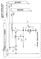
表示パネル部100は、基板101の上に、画素回路Pがn行×m列のマトリクス状に配列された画素アレイ部102と、画素回路Pを垂直方向に走査する垂直駆動部103と、画素回路Pを水平方向に走査する水平駆動部(水平セレクタあるいはデータ線駆動部とも称される)106と、各駆動部103,106と外部回路とのインタフェースをとるインタフェース(IF)部130と、外部接続用の端子部(パッド部)108などが集積形成されている。すなわち、垂直駆動部103や水平駆動部106やインタフェース部130などの周辺駆動回路が、画素アレイ部102と同一の基板101上に形成された構成となっている。
The display panel unit 100 includes a
インタフェース部130は、垂直駆動部103と外部回路とのインタフェースをとる垂直IF部133と、水平駆動部106と外部回路とのインタフェースをとる水平IF部136を有する。
The interface unit 130 includes a vertical IF
垂直駆動部103(書込走査部104および駆動走査部105)と水平駆動部106とで、信号電位の保持容量への書込みや、閾値補正動作や、移動度補正動作や、ブートストラップ動作を制御する制御部109が構成される。この制御部109とインタフェース部130(垂直IF部133や水平IF部136)を含めて、画素アレイ部102の画素回路Pを駆動する駆動回路を構成している。
The vertical driving unit 103 (the writing
垂直駆動部103としては、たとえば、書込走査部(ライトスキャナWS;Write Scan)104や電源供給能力を有する電源スキャナとして機能する駆動走査部(ドライブスキャナDS;Drive Scan)105を有する。 画素アレイ部102は、一例として、図示する左右方向の一方側もしくは両側から書込走査部104および駆動走査部105で駆動され、かつ図示する上下方向の一方側もしくは両側から水平駆動部106で駆動されるようになっている。
The
端子部108には、表示装置1の外部に配された駆動信号生成部200から、種々のパルス信号が供給されるようになっている。また同様に、映像信号処理部220から映像信号Vsig (カラー表示の場合には色別の映像信号Vsig_R,G,B)が供給されるようになっている。
Various pulse signals are supplied to the
一例としては、垂直駆動用のパルス信号として、垂直方向の書込み開始パルスの一例であるシフトスタートパルスSPDS,SPWSや垂直走査クロックCKDS,CKWS(必要に応じて位相反転した垂直走査クロックxCKDS ,xCKWS も)など必要なパルス信号が供給される。また、水平駆動用のパルス信号として、水平方向の書込み開始パルスの一例である水平スタートパルスSPH や水平走査クロックCKH (必要に応じて位相反転した水平走査クロックxCKHも)など必要なパルス信号が供給される。 For example, as a pulse signal for vertical driving, shift start pulses SPDS and SPWS which are examples of vertical write start pulses and vertical scanning clocks CKDS and CKWS (vertical scanning clocks xCKDS and xCKWS whose phases are reversed as necessary) ) And other necessary pulse signals are supplied. In addition, as a pulse signal for horizontal driving, necessary pulse signals such as a horizontal start pulse SPH, which is an example of a horizontal write start pulse, and a horizontal scanning clock CKH (and a horizontal scanning clock xCKH whose phase is inverted as necessary) are supplied. Is done.
端子部108の各端子は、配線109を介して、垂直駆動部103や水平駆動部106に接続されるようになっている。たとえば、端子部108に供給された各パルスは、必要に応じて図示を割愛したレベルシフタ部で電圧レベルを内部的に調整した後、バッファを介して垂直駆動部103の各部や水平駆動部106に供給される。
Each terminal of the
画素アレイ部102は、図示を割愛するが(詳細は後述する)、表示素子としての有機EL素子に対して画素トランジスタが設けられた画素回路Pが行列状に2次元配置され、この画素配列に対して行ごとに走査線が配線されるとともに、列ごとに信号線が配線された構成となっている。
Although the
たとえば、画素アレイ部102には、走査線(ゲート線)104WSと映像信号線(データ線)106HSが形成されている。両者の交差部分には図示を割愛した有機EL素子とこれを駆動する薄膜トランジスタが形成される。有機EL素子と薄膜トランジスタの組み合わせで画素回路Pを構成する。
For example, in the
具体的には、マトリクス状に配列された各画素回路Pに対しては、書込走査部104によって書込駆動パルスWSで駆動されるn行分の書込走査線104WS_1〜104WS_nおよび駆動走査部105によって電源駆動パルスDSL で駆動されるn行分の電源供給線105DSL_1 〜105DSL_n が画素行ごとに配線される。
Specifically, for each pixel circuit P arranged in a matrix, the write scanning lines 104WS_1 to 104WS_n for n rows driven by the
書込走査部104および駆動走査部105は、論理ゲートの組合せ(ラッチやシフトレジスタなども含む)によって構成され、画素アレイ部102の各画素回路Pを行単位で選択する、すなわち、駆動信号生成部200から供給される垂直駆動系のパルス信号に基づき、書込走査線104WSおよび電源供給線105DSL を介して各画素回路Pを順次選択する。
The writing
水平駆動部106は、論理ゲートの組合せ(ラッチやシフトレジスタなども含む)によって構成され、画素アレイ部102の各画素回路Pを列単位で選択する、すなわち、駆動信号生成部200から供給される水平駆動系のパルス信号に基づき、選択された画素回路Pに対し映像信号線106HSを介して映像信号Vsig の内の所定電位をサンプリングして保持容量に書き込ませる。
The
本実施形態の表示装置1は、線順次駆動や点順次駆動が可能になっており、垂直駆動部103の書込走査部104および駆動走査部105は線順次で(つまり行単位で)で画素アレイ部102を走査するとともに、これに同期して水平駆動部106が、画像信号を、1水平ライン分を同時に(線順次の場合)、あるいは画素単位で(点順次の場合)、画素アレイ部102に書き込む。
The
なお、図1では、画素アレイ部102の一方側にのみ垂直駆動部103を配置する構成を示しているが、画素アレイ部102を挟んで左右両側に垂直駆動部103を配置する構成を採ることも可能である。同様に、図1では、画素アレイ部102の一方側にのみ水平駆動部106を配置する構成を示しているが、画素アレイ部102を挟んで上下両側に水平駆動部106を配置する構成を採ることも可能である。
FIG. 1 shows a configuration in which the
なお、本例では、シフトスタートパルスSPDS,SPWS、垂直走査クロックCKDS,CKWSや水平スタートパルスSPH 、水平走査クロックCKH などのパルス信号を表示パネル部100の外部から入力する構成としているが、これらの各種のタイミングパルスを生成する駆動信号生成部200を表示パネル部100上に搭載することも可能である。
In this example, pulse signals such as shift start pulses SPDS and SPWS, vertical scanning clocks CKDS and CKWS, horizontal start pulse SPH and horizontal scanning clock CKH are input from the outside of the display panel unit 100. A drive
<画素回路>
図2および図2Aは、本実施形態の基本構成の画素回路Pと、当該画素回路Pを備えた有機EL表示装置の一実施形態を示す図である。本実施形態の基本構成の画素回路Pを画素アレイ部102に備える表示装置1を本実施形態の基本構成の表示装置1と称する。図2は基本構成を示し、図2Aは具体的な構成を示す。なお、表示パネル部100の基板101上において画素回路Pの周辺部に設けられた垂直駆動部103と水平駆動部106も合わせて示している。図3は、有機EL素子127や駆動トランジスタ121の特性ばらつきが駆動電流Idsに与える影響を説明する図であり、図3Aは、その改善手法の概念を説明する図である。
<Pixel circuit>
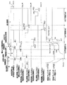
2 and 2A are diagrams showing an embodiment of a pixel circuit P having a basic configuration of the present embodiment and an organic EL display device including the pixel circuit P. FIG. The
pチャネル型のトランジスタではなく、nチャネル型のトランジスタで駆動トランジスタを構成することができれば、トランジスタ作成において従来のアモルファスシリコン(a−Si)プロセスを用いることが可能になる。これにより、トランジスタ基板の低コスト化が可能となり、このような構成の画素回路Pの開発が期待される。 If a driving transistor can be formed of an n-channel transistor instead of a p-channel transistor, a conventional amorphous silicon (a-Si) process can be used in transistor formation. Thereby, the cost of the transistor substrate can be reduced, and the development of the pixel circuit P having such a configuration is expected.
駆動トランジスタを始めとする各トランジスタとしてはMOSトランジスタを使用する。この場合、駆動トランジスタについては、ゲート端を制御入力端として取り扱い、ソース端およびドレイン端の何れか一方(ここではソース端とする)を出力端として取り扱い、他方を電源供給端(ここではドレイン端とする)として取り扱う。 MOS transistors are used as the transistors including the drive transistor. In this case, for the drive transistor, the gate end is handled as the control input end, and either the source end or the drain end (here, the source end) is handled as the output end, and the other is the power supply end (here, the drain end). ).
図2および図2Aに示す本実施形態の画素回路Pは、基本的にnチャネル型の薄膜電界効果トランジスタでドライブトランジスタが構成されている点に特徴を有する。また、有機EL素子の経時劣化による当該有機EL素子への駆動電流Idsの変動を抑制するための回路、すなわち電気光学素子の一例である有機EL素子の電流−電圧特性の変化を補正して駆動電流Idsを一定に維持する駆動信号一定化回路(その1)を備え、また駆動トランジスタの特性変動(閾値電圧ばらつきや移動度ばらつき)による駆動電流変動を防ぐ閾値補正機能や移動度補正機能を実現して駆動電流Idsを一定に維持する駆動方式を採用した点に特徴を有する。 The pixel circuit P of the present embodiment shown in FIGS. 2 and 2A is characterized in that a drive transistor is basically composed of an n-channel thin film field effect transistor. In addition, a circuit for suppressing fluctuations in the drive current Ids to the organic EL element due to deterioration over time of the organic EL element, that is, driving by correcting a change in current-voltage characteristics of the organic EL element which is an example of an electro-optical element A drive signal stabilization circuit (part 1) that maintains the current Ids constant is provided, and a threshold correction function and mobility correction function that prevents drive current fluctuations due to drive transistor characteristic fluctuations (threshold voltage fluctuations and mobility fluctuations) are realized. Thus, the present embodiment is characterized in that a driving method for keeping the driving current Ids constant is adopted.
駆動トランジスタ121の特性変動(たとえば閾値電圧や移動度などのばらつきや変動)による駆動電流Idsに与える影響を抑制する方法としては、2TR構成の駆動回路をそのまま駆動信号一定化回路(その1)として採用しつつ、各トランジスタ121,125の駆動タイミングを工夫することで対処する。
As a method of suppressing the influence on the drive current Ids due to the characteristic variation of the drive transistor 121 (for example, variation or fluctuation in threshold voltage, mobility, etc.), the 2TR configuration drive circuit is used as it is as a drive signal stabilization circuit (part 1). This is dealt with by devising the drive timing of the
また、本実施形態の画素回路Pは、2TR駆動の構成であり、素子数や配線数が少ないため、高精細化が可能であることに加えて、映像信号Vsig の劣化なくサンプリングできるため、良好な画質を得ることができる。 In addition, the pixel circuit P of the present embodiment has a 2TR drive configuration, and since the number of elements and wirings is small, high definition is possible, and in addition, sampling is possible without deterioration of the video signal Vsig. Image quality can be obtained.
また本実施形態の画素回路Pは、保持容量120の接続態様に特徴を有し、有機EL素子127の経時劣化による駆動電流変動を防ぐ回路として、駆動信号一定化回路(その2)の一例であるブートストラップ回路を構成している。有機EL素子の電流−電圧特性に経時変化があった場合でも駆動電流を一定にする(駆動電流変動を防ぐ)ブートストラップ機能を実現する駆動信号一定化回路(その2)を備えた点に特徴を有するのである。
The pixel circuit P of the present embodiment is characterized by the connection mode of the
詳細は後述するが、本実施形態の画素回路Pは、書込みゲインやブートストラップゲインや移動度補正期間に関係する補助容量を備える。ただし、この補助容量を備えることは必須ではない。本実施形態の画素回路Pを駆動するに当たっての基本的な制御動作は、補助容量を備えていない画素回路Pに対するものと同様である。 Although details will be described later, the pixel circuit P of the present embodiment includes an auxiliary capacitor related to a write gain, a bootstrap gain, and a mobility correction period. However, it is not essential to provide this auxiliary capacity. The basic control operation for driving the pixel circuit P of the present embodiment is the same as that for the pixel circuit P that does not include an auxiliary capacitor.
具体的には図2および図2Aに示すように、本実施形態の画素回路Pは、それぞれnチャネル型の駆動トランジスタ121およびサンプリングトランジスタ125と、電流が流れることで発光する電気光学素子の一例である有機EL素子127とを有する。一般に、有機EL素子127は整流性があるためダイオードの記号で表している。なお、有機EL素子127には、寄生容量Celが存在する。図では、この寄生容量Celを有機EL素子127(ダイオード状のもの)と並列に示す。
Specifically, as shown in FIG. 2 and FIG. 2A, the pixel circuit P of the present embodiment is an example of an n-
駆動トランジスタ121は、ドレイン端Dが第1電源電位を供給する電源供給線DSL に接続され、ソース端(出力端)Sが、有機EL素子127のアノード端Aに接続され(その接続点をノードND121とする)、有機EL素子127のカソード端Kが基準電位を供給する全画素共通の接地配線Vcath(GND )に接続されている。
The
なお、接地配線Vcathは、それ用の単一層の配線(上層配線)のみとしてもよいし、たとえばアノード用の配線が形成されるアノード層に、カソード配線用の補助配線を設けてカソード配線の抵抗値を低減するようにしてもよい。この補助配線は、表示エリア内に格子状または列または行状に配線され、上層配線と同電位で固定電位である。 The ground wiring Vcath may be only a single-layer wiring (upper layer wiring) for the ground wiring Vcath. For example, an auxiliary wiring for the cathode wiring is provided on the anode layer where the wiring for the anode is formed, and the resistance of the cathode wiring is set. The value may be reduced. The auxiliary wiring is wired in a lattice shape, a column, or a row in the display area, and has a fixed potential at the same potential as the upper layer wiring.
サンプリングトランジスタ125は、ゲート端Gが書込走査部104からの書込走査線104WSに接続され、ドレイン端Dが映像信号線106HSに接続され、ソース端Sが駆動トランジスタ121のゲート端Gに接続されている(その接続点をノードND122とする)。サンプリングトランジスタ125のゲート端Gには、書込走査部104からアクティブHの書込駆動パルスWSが供給される。サンプリングトランジスタ125は、ソース端Sとドレイン端Dとを逆転させた接続態様とすることもできる。
The
駆動トランジスタ121のドレイン端Dは、電源スキャナとして機能する駆動走査部105からの電源供給線105DSL に接続されている。電源供給線105DSL は、この電源供給線105DSL そのものが、駆動トランジスタ121に対しての電源供給能力を備える点に特徴を有する。
The drain terminal D of the
駆動走査部105は、駆動トランジスタ121のドレイン端Dに対して、それぞれ電源電圧に相当する高電圧側の第1電位Vcc_Hと閾値補正に先立つ準備動作に利用される低電圧側の第2電位Vcc_L(初期化電圧もしくはイニシャル電圧Vini とも称される)とを切り替えて供給する。
The
駆動トランジスタ121のドレイン端D側を第1電位Vcc_Hと第2電位Vcc_Lの2値をとる電源駆動パルスDSL で駆動することで、閾値補正に先立つ準備動作を行なうことを可能にしている。
By driving the drain terminal D side of the driving
第2電位Vcc_Lとしては、映像信号線106HSにおける映像信号Vsig の基準電位Vo(オフセット電圧Vofs とも称する)より十分低い電位とする。具体的には、駆動トランジスタ121のゲート・ソース間電圧Vgs(ゲート電位Vgとソース電位Vsの差)が駆動トランジスタ121の閾値電圧Vthより大きくなるように、電源供給線105DSL の低電位側の第2電位Vcc_Lを設定する。なお、基準電位Vo(Vofs )は、閾値補正動作に先立つ初期化動作に利用するとともに映像信号線106HSを予めプリチャージにしておくためにも利用する。
The second potential Vcc_L is a potential that is sufficiently lower than the reference potential Vo (also referred to as offset voltage Vofs) of the video signal Vsig in the video signal line 106HS. Specifically, the gate-source voltage Vgs of the drive transistor 121 (the difference between the gate potential Vg and the source potential Vs) is larger than the threshold voltage Vth of the
このような画素回路Pでは、有機EL素子127を駆動するときには、駆動トランジスタ121のドレイン端Dに第1電位Vcc_Hが供給され、ソース端Sが有機EL素子127のアノード端A側に接続されることで、全体としてソースフォロワ回路を形成するようになっている。
In such a pixel circuit P, when driving the
このような画素回路Pを採用する場合、駆動トランジスタ121の他に走査用に1つのスイッチングトランジスタ(サンプリングトランジスタ125)を使用する2TR駆動の構成を採るとともに、各スイッチングトランジスタを制御する電源駆動パルスDSL および書込駆動パルスWSのオン/オフタイミングの設定により、有機EL素子127の経時劣化や駆動トランジスタ121の特性変動(たとえば閾値電圧や移動度などのばらつきや変動)による駆動電流Idsに与える影響を防ぐ点に特徴を有する。
When such a pixel circuit P is employed, a 2TR driving configuration using one switching transistor (sampling transistor 125) for scanning in addition to the driving
加えて、本実施形態の表示装置1においては、画素回路Pごとに、ノードND121(駆動トランジスタ121のソース端Sおよび保持容量120の一方の端子と有機EL素子127のアノード端Aの接続点)に容量値Csub の容量素子である補助容量310を追加し、補助容量310の他方の端子(ノードND310と称する)の接続箇所を自行(自段)の電源供給線105DSL とする点に特徴を有する。補助容量310は、有機EL素子127(その寄生容量Cel)と電気回路的に並列接続されたものとなる。
In addition, in the
本実施形態では、図2Aに具体例を示すように、ノードND310を有機EL素子127のカソード配線に接続することにする。ノードND310の接続点は、本実施形態では、有機EL素子127のカソード配線としているが、これ以外にも、たとえば自段(行)の電源供給線105DSL とすることや、自段(行)以外の電源供給線105DSL とすることや、任意の値(接地電位を含む)の固定電位とすることも考えられる。ノードND310の接続点が何れであるかによって、それぞれ長短(利点と欠点)があるが、ここではその説明を割愛する。
In the present embodiment, the node ND310 is connected to the cathode wiring of the
自行以外としては、当該行の電源供給線105DSL より前段側に属する別の電源供給線105DSL とすることや、当該行の電源供給線105DSL より後段側に属する別の電源供給線105DSL とすることが考えられる。たとえば、直前よりもさらにその前の電源供給線105DSL に接続してもよい。もちろん、ノードND310を直後の行(1水平期間後:後側の隣接行)の電源供給線105DSL に接続してもよい。ただしこれらは前段側や後段側の一例であって、これに限られるものではなく、たとえば、直前よりもさらにその前の電源供給線105DSL あるいは直後よりもさらにその後ろの電源供給線105DSL に接続してもよい。ただし、隣接行以外ではその分配線長が長くなり配線抵抗やクロストークノイズなどの難点が懸念される。この点においては自段以外に接続する際には、ノードND310を隣接行の電源供給線105DSL に接続するのがよい。 Other than the own line, another power supply line 105DSL belonging to the preceding stage from the power supply line 105DSL of the row or another power supply line 105DSL belonging to the subsequent stage from the power supply line 105DSL of the row may be used. Conceivable. For example, the power supply line 105DSL may be connected to the power supply line 105DSL immediately before it. Of course, the node ND310 may be connected to the power supply line 105DSL in the next row (after one horizontal period: the adjacent row on the rear side). However, these are examples of the front side and the rear side, and are not limited thereto. For example, they are connected to the power supply line 105DSL before and immediately before or immediately after the power supply line 105DSL. May be. However, other than adjacent rows, the wiring length is correspondingly increased, and there are concerns about problems such as wiring resistance and crosstalk noise. In this regard, it is preferable to connect the node ND310 to the power supply line 105DSL in the adjacent row when connecting to other than the own stage.
また、ノードND310を固定電位にする際には、たとえば、全ての有機EL素子127のカソード端Kが接続される全画素共通の接地配線Vcath(上層配線でもよいし補助配線でもよい)とすることも考えられる。あるいは、ノードND310用に専用の固定電位を与えるため、TFT層で配線を設けてもよい。なお、このTFT層の補助容量310用の配線をカソード配線と兼用してもよい。
Further, when the node ND310 is set to a fixed potential, for example, the ground wiring Vcath common to all pixels to which the cathode ends K of all the
<基本動作>
先ず、図2および図2Aに示す本実施形態の画素回路Pの特徴を説明する上での比較例として、図示を割愛するが、補助容量310を備えておらず、保持容量120は、一方の端子がノードND122に接続され、他方の端子が全画素共通の接地配線Vcath(GND )に接続されている場合での動作について説明する。以下、このような画素回路Pを第1比較例の画素回路Pと称する。またここでは図示を割愛するが(後述の図5を参照)、本実施形態の画素回路Pから補助容量310を外した構成を第2比較例の画素回路Pと称する。
<Basic operation>
First, as a comparative example for explaining the characteristics of the pixel circuit P of the present embodiment shown in FIG. 2 and FIG. 2A, the illustration is omitted, but the
第1比較例の画素回路Pに対する変形例として、発光期間を制御する発光制御トランジスタを追加した3TR型とする場合、たとえば、駆動トランジスタ121のソース端をnチャネル型の発光制御トランジスタのドレイン端Dに接続し、発光制御トランジスタのソース端Sを有機EL素子127のアノード端に接続する。
As a modification of the pixel circuit P of the first comparative example, when the 3TR type is added with a light emission control transistor for controlling the light emission period, for example, the source end of the
第1比較例(3TR型とした変形例も含む)の画素回路Pでは、発光制御トランジスタを設けるか否かに関わらず、有機EL素子127を駆動するときには、駆動トランジスタ121のドレイン端D側が第1電源電位に接続され、ソース端Sが有機EL素子127のアノード端A側に接続されることで、全体としてソースフォロワ回路を形成するようになっている。
In the pixel circuit P of the first comparative example (including the modified example of 3TR type), when the
第1比較例の画素回路Pを駆動する際のタイミングチャートの図示は割愛するが、映像信号線106HSが映像信号Vsig の有効期間である信号電位にある時間帯に、書込走査線WSの電位が高レベルに遷移することで、nチャネル型のサンプリングトランジスタ125はオン状態となり、信号線HSから供給される映像信号線電位を保持容量120に充電する。この期間が映像信号Vsig のサンプリング期間となり、それ以降が保持期間となる。これにより駆動トランジスタ121のゲート端Gの電位(ゲート電位Vg)は上昇を開始し、ドレイン電流を流し始める。そのため、有機EL素子127のアノード電位は上昇し発光を開始する。
Although illustration of a timing chart when driving the pixel circuit P of the first comparative example is omitted, the potential of the write scanning line WS is in a time zone in which the video signal line 106HS is in the signal potential that is the effective period of the video signal Vsig. Transitions to a high level, the n-
この後、書込駆動パルスWSが低レベルに遷移すると、保持容量120にその時点の映像信号線電位、つまり、映像信号Vsig の電位の内の有効期間の電位(信号電位)が保持される。これによって、駆動トランジスタ121のゲート電位Vgが一定となり、発光輝度が次のフレーム(またはフィールド)まで一定に維持される。
Thereafter, when the write drive pulse WS transitions to a low level, the holding
ここで、第1比較例の画素回路Pでは、駆動トランジスタ121のソース端Sの電位(ソース電位Vs)は、駆動トランジスタ121と有機EL素子127との動作点で決まり、その電圧値は駆動トランジスタ121のゲート電位Vgによって異なる値を持ってしまう。
Here, in the pixel circuit P of the first comparative example, the potential of the source terminal S of the drive transistor 121 (source potential Vs) is determined by the operating point of the
一般的に、MOS型の駆動トランジスタ121は飽和領域で駆動される。よって、飽和領域で動作するトランジスタのドレイン端−ソース間に流れる電流をIds、移動度をμ、チャネル幅(ゲート幅)をW、チャネル長(ゲート長)をL、ゲート容量(単位面積当たりのゲート酸化膜容量)をCoxは、トランジスタの閾値電圧をVthとすると、駆動トランジスタ121は下記の式(1)に示した値を持つ定電流源となっている。式(1)から明らかなように、飽和領域ではトランジスタのドレイン電流Idsはゲート・ソース間電圧Vgsによって制御される。
In general, the MOS

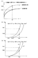
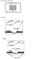
<有機EL素子のI−V特性>
図3(1)に示す有機EL素子の電流−電圧(I−V)特性において、実線で示す曲線が初期状態時の特性を示し、破線で示す曲線が経時変化後の特性を示している。一般的に有機EL素子のI−V特性は、グラフに示すように時間が経過すると劣化する。
<IV characteristics of organic EL element>
In the current-voltage (IV) characteristics of the organic EL element shown in FIG. 3A, the curve indicated by the solid line indicates the characteristic in the initial state, and the curve indicated by the broken line indicates the characteristic after change with time. Generally, the IV characteristic of an organic EL element deteriorates with time as shown in the graph.
第1比較例の画素回路Pでは、この経時劣化により動作点が変化してしまい、同じゲート電位Vgを印加しても駆動トランジスタ121のソース電位Vsは変化してしまう。これにより、駆動トランジスタ121のゲート・ソース間電圧Vgsは変化してしまう。特性式(1)から明らかなように、ゲート・ソース間電圧Vgsが変動すると、たとえゲート電位Vgが一定であっても駆動電流Idsが変動し、同時に有機EL素子127に流れる電流値も変化する。このように有機EL素子127のI−V特性が変化すると、図2に示したソースフォロワ構成を持つ第1比較例の画素回路Pでは、有機EL素子127の発光輝度が経時的に変化してしまう。
In the pixel circuit P of the first comparative example, the operating point changes due to deterioration with time, and the source potential Vs of the
駆動トランジスタ121としてnチャネル型を使用した単純な回路では、ソース端Sが有機EL素子127側に接続されてしまうため、有機EL素子127の経時変化とともに、ゲート・ソース間電圧Vgsが変化してしまい、有機EL素子127に流れる電流量が変化し、その結果、発光輝度は変化してしまうのである。
In a simple circuit using an n-channel type as the driving
発光素子の一例である有機EL素子127の特性の経時変動による有機EL素子127のアノード電位変動は、駆動トランジスタ121のゲート・ソース間電圧Vgsの変動となって現れ、ドレイン電流(駆動電流Ids)の変動を引き起こす。この原因による駆動電流の変動は画素回路Pごとの発光輝度のばらつきとなって現れ、画質の劣化が起きる。
A variation in the anode potential of the
これに対して、詳細は後述するが、駆動トランジスタ121のソース端Sの電位Vsの変動にゲート端Gの電位Vgが連動するようにするブートストラップ機能を実現する回路構成および駆動タイミングとすることで、有機EL素子127の特性の経時変動による有機EL素子127のアノード電位変動(つまりソース電位変動)があっても、その変動を相殺するようにゲート電位Vgを変動させることで、画面輝度の均一性(ユニフォーミティ)を確保できる。ブートストラップ機能が、有機EL素子を代表とする電流駆動型の発光素子の経時劣化補正能力を向上させることができる。
On the other hand, as will be described in detail later, a circuit configuration and a driving timing for realizing a bootstrap function in which the potential Vg of the gate terminal G is interlocked with the fluctuation of the potential Vs of the source terminal S of the driving
もちろん、このブートストラップ機能は、発光開始時点で、有機EL素子127に発光電流Ielが流れ始め、それによってアノード・カソード間電圧Velが安定となるまで上昇していく過程で、そのアノード・カソード間電圧Velの変動に伴って駆動トランジスタ121のソース電位Vsが変動する際にも機能する。
Of course, in the bootstrap function, the light emission current Iel begins to flow through the
<駆動トランジスタのVgs−Ids特性>
また、駆動トランジスタ121の製造プロセスのばらつきにより、画素回路Pごとに閾値電圧や移動度などの特性変動がある。駆動トランジスタ121を飽和領域で駆動する場合においても、この特性変動により、駆動トランジスタ121に同一のゲート電位を与えても、画素回路Pごとにドレイン電流(駆動電流Ids)が変動し、発光輝度のばらつきになって現れる。
<Vgs-Ids characteristics of drive transistor>
In addition, due to variations in the manufacturing process of the
たとえば、図3(2)は、駆動トランジスタ121の閾値ばらつきに着目した電圧電流(Vgs−Ids)特性を示す図である。閾値電圧がVth1とVth2で異なる2個の駆動トランジスタ121について、それぞれ特性カーブを挙げてある。
For example, FIG. 3B is a diagram illustrating the voltage-current (Vgs-Ids) characteristics focusing on the threshold variation of the
前述のように、駆動トランジスタ121が飽和領域で動作しているときのドレイン電流Idsは、特性式(1)で表される。特性式(1)から明らかなように、閾値電圧Vthが変動すると、ゲート・ソース間電圧Vgsが一定であってもドレイン電流Idsが変動する。つまり、閾値電圧Vthのばらつきに対して何ら対策を施さないと、図3(2)に示すように、閾値電圧がVth1のときVgsに対応する駆動電流がIds1となるのに対して、閾値電圧がVth2のときの同じゲート電圧Vgsに対応する駆動電流Ids2はIds1と異なってしまう。
As described above, the drain current Ids when the driving
また、図3(3)は、駆動トランジスタ121の移動度ばらつきに着目した電圧電流(Vgs−Ids)特性を示す図である。移動度がμ1とμ2で異なる2個の駆動トランジスタ121について、それぞれ特性カーブを挙げてある。
FIG. 3 (3) is a diagram showing voltage-current (Vgs-Ids) characteristics focusing on the mobility variation of the
特性式(1)から明らかなように、移動度μが変動すると、ゲート・ソース間電圧Vgsが一定であってもドレイン電流Idsが変動する。つまり、移動度μのばらつきに対して何ら対策を施さないと、図3(3)に示すように、移動度がμ1のときゲート・ソース間電圧Vgsに対応する駆動電流がIds1となるのに対して、移動度がμ2のときの同じゲート・ソース間電圧Vgsに対応する駆動電流Ids2はIds1と異なってしまう。 As apparent from the characteristic equation (1), when the mobility μ varies, the drain current Ids varies even when the gate-source voltage Vgs is constant. In other words, if no measures are taken against the variation in mobility μ, the drive current corresponding to the gate-source voltage Vgs becomes Ids1 when the mobility is μ1, as shown in FIG. On the other hand, the drive current Ids2 corresponding to the same gate-source voltage Vgs when the mobility is μ2 is different from Ids1.
<閾値補正および移動度補正の概念>
これに対して、閾値補正機能および移動度補正機能を実現する駆動タイミング(詳細は後述する)とすることで、図3Aの各図から理解されるように、それらの変動の影響を抑制でき、画面輝度の均一性(ユニフォーミティ)を確保できる。
<Concept of threshold correction and mobility correction>
On the other hand, by setting the drive timing (details will be described later) to realize the threshold value correction function and the mobility correction function, as can be understood from each diagram of FIG. Uniformity of screen brightness can be ensured.
本実施形態の閾値補正動作および移動度補正動作では、詳細は後述するが、書込みゲインが1(理想値)であると仮定した場合、発光時のゲート・ソース間電圧Vgsが“Vin+Vth−ΔV”で表されるようにすることで、ドレイン・ソース間電流Idsが、閾値電圧Vthのばらつきや変動に依存しないようにするとともに、移動度μのばらつきや変動に依存しないようにする。結果として、閾値電圧Vthや移動度μが製造プロセスにより変動しても、駆動電流Idsは変動せず、有機EL素子127の発光輝度も変動しない。
Although details will be described later in the threshold value correcting operation and the mobility correcting operation of this embodiment, when it is assumed that the writing gain is 1 (ideal value), the gate-source voltage Vgs at the time of light emission is “Vin + Vth−ΔV”. Thus, the drain-source current Ids is not dependent on the variation or variation of the threshold voltage Vth, and is not dependent on the variation or variation of the mobility μ. As a result, even if the threshold voltage Vth and the mobility μ vary depending on the manufacturing process, the drive current Ids does not vary, and the light emission luminance of the
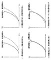
たとえば、図3Aの各図においては、駆動トランジスタ121の電流電圧特性を、横軸に信号振幅Vinをとり、縦軸に駆動電流Idsをとって、閾値電圧Vthが比較的低く移動度μが比較的大きい駆動トランジスタ121で構成された画素回路Pa(実線のカーブ)と、逆に閾値電圧Vthが比較的高く移動度μが比較的小さい駆動トランジスタ121で構成された画素回路Pb(点線のカーブ)について、それぞれ特性カーブを挙げてある。
For example, in each diagram of FIG. 3A, the current-voltage characteristics of the
図3A(1)は、閾値補正および移動度補正ともに実行しない場合である。このときには画素回路Paおよび画素回路Pbで閾値電圧Vthおよび移動度μの補正が全く実行されないため、閾値電圧Vthや移動度μの違いでVin−Ids特性に大きな違いが出てしまう。したがって、同じ信号振幅Vinを与えても、駆動電流Idsすなわち発光輝度が異なってしまい、画面輝度の均一性(ユニフォーミティ)が得られない。 FIG. 3A (1) shows a case where neither threshold correction nor mobility correction is executed. At this time, since the threshold voltage Vth and the mobility μ are not corrected at all in the pixel circuit Pa and the pixel circuit Pb, the difference in the threshold voltage Vth and the mobility μ causes a large difference in Vin-Ids characteristics. Therefore, even if the same signal amplitude Vin is given, the drive current Ids, that is, the light emission luminance differs, and the uniformity of the screen luminance (uniformity) cannot be obtained.
図3A(2)は、閾値補正を実行する一方、移動度補正を実行しない場合である。このとき画素回路Paと画素回路Pbで閾値電圧Vthの違いはキャンセルされる。しかしながら移動度μの相違はそのまま現れている。したがって信号振幅Vinが高い領域(すなわち輝度が高い領域)で、移動度μの違いが顕著に現れ、同じ階調でも輝度が違ってしまう。具体的には、同じ階調(同じ信号振幅Vin)で、移動度μの大きい画素回路Paの輝度(駆動電流Ids)は高く、移動度μの小さい画素回路Pbの輝度は低くなる。 FIG. 3A (2) shows a case where threshold correction is performed while mobility correction is not performed. At this time, the difference in threshold voltage Vth between the pixel circuit Pa and the pixel circuit Pb is cancelled. However, the difference in mobility μ appears as it is. Therefore, in the region where the signal amplitude Vin is high (that is, the region where the luminance is high), the difference in mobility μ appears remarkably, and the luminance is different even in the same gradation. Specifically, at the same gradation (same signal amplitude Vin), the luminance (drive current Ids) of the pixel circuit Pa having a high mobility μ is high, and the luminance of the pixel circuit Pb having a low mobility μ is low.
図3A(3)は閾値補正および移動度補正ともに実行する場合である。閾値電圧Vthおよび移動度μの相違は完全に補正され、その結果、画素回路Paと画素回路PbのVin−Ids特性は一致する。したがって、全ての階調(信号振幅Vin)で輝度(Ids)が同一レベルとなり、画面輝度の均一性(ユニフォーミティ)が顕著に改善される。 FIG. 3A (3) shows a case where both threshold value correction and mobility correction are executed. The difference between the threshold voltage Vth and the mobility μ is completely corrected. As a result, the Vin-Ids characteristics of the pixel circuit Pa and the pixel circuit Pb match. Therefore, the luminance (Ids) becomes the same level in all the gradations (signal amplitude Vin), and the uniformity of the screen luminance (uniformity) is remarkably improved.
図3A(4)は、閾値補正および移動度補正ともに実行するものの、閾値電圧Vthの補正が不十分な場合である。たとえば、1回の閾値補正動作では駆動トランジスタ121の閾値電圧Vthに相当する電圧を十分に保持容量120へ保持させることができない場合がその一例である。このときには、閾値電圧Vthの差が除去されないため、画素回路Paと画素回路Pbでは低階調の領域で輝度(駆動電流Ids)に差が出てしまう。よって、閾値電圧Vthの補正が不十分な場合は低階調で輝度のムラが現れ画質を損なうことになる。
FIG. 3A (4) shows a case where both threshold correction and mobility correction are executed, but the correction of the threshold voltage Vth is insufficient. For example, a case where a voltage corresponding to the threshold voltage Vth of the
<画素回路の動作>
第1比較例の画素回路Pにおける有機EL素子127の経時劣化による駆動電流変動を防ぐ回路(ブートストラップ回路)を搭載し、また駆動トランジスタ121の特性変動(閾値電圧ばらつきや移動度ばらつき)による駆動電流変動を防ぐ駆動方式を採用したのが図2および図2Aに示す本実施形態や図示しない第2比較例(補助容量310を備えていない構成)の画素回路Pである。
<Operation of pixel circuit>
The pixel circuit P of the first comparative example is equipped with a circuit (bootstrap circuit) that prevents fluctuations in the driving current due to deterioration with time of the
第2比較例(事実上、本実施形態の画素回路Pも同様;以下駆動タイミングに関して同様)の画素回路Pにおいて、駆動タイミングとしては、先ず、サンプリングトランジスタ125は、書込走査線104WSから供給された書込駆動パルスWSに応じて導通し、映像信号線106HSから供給された映像信号Vsig をサンプリングして保持容量120に保持する。この点は、基本的には、第1比較例の画素回路Pを駆動する場合と同じである。
In the pixel circuit P of the second comparative example (in fact, the same applies to the pixel circuit P of the present embodiment; the same applies to the driving timing hereinafter), the
以下では、説明や理解を容易にするため、特段の断りのない限り、書込みゲインが1(理想値)であると仮定して、保持容量120に信号振幅Vinの情報を、書き込む、保持する、あるいはサンプリングするなどと簡潔に記して説明する。書込みゲインが1未満の場合、保持容量120には信号振幅Vinの大きさそのものではなく、信号振幅Vinの大きさに対応するゲイン倍された情報が保持されることになる。
In the following, for ease of explanation and understanding, unless otherwise specified, it is assumed that the write gain is 1 (ideal value), and information on the signal amplitude Vin is written and held in the holding
なお、第2比較例の画素回路Pにおける駆動タイミングは、映像信号Vsig の信号振幅Vinの情報を保持容量120に書き込む際に、順次走査の観点からは、1行分の映像信号を同時に各列の映像信号線106HSに伝達する線順次駆動を行なう。
Note that the drive timing in the pixel circuit P of the second comparative example is such that when the information of the signal amplitude Vin of the video signal Vsig is written in the holding
駆動トランジスタ121は、第1電位(高電位側)にある電源供給線105DSL から電流の供給を受け保持容量120に保持された信号電位(映像信号Vsig の有効期間の電位に対応する電位)に応じて駆動電流Idsを有機EL素子127に流す。
The driving
垂直駆動部103は、電源供給線105DSL が第1電位にありかつ映像信号線106HSが映像信号Vsig の非有効期間である基準電位Vo(Vofs )にある時間帯でサンプリングトランジスタ125を導通させる制御信号として書込駆動パルスWSを出力して、駆動トランジスタ121の閾値電圧Vthに相当する電圧を保持容量120に保持しておく。この動作が閾値補正機能を実現する。この閾値補正機能により、画素回路Pごとにばらつく駆動トランジスタ121の閾値電圧Vthの影響をキャンセルすることができる。
The
第2比較例の画素回路Pにおける駆動タイミングとしては、垂直駆動部103は、映像信号Vsig の内の信号振幅Vinのサンプリングに先行する複数の水平期間で閾値補正動作を繰り返し実行して確実に駆動トランジスタ121の閾値電圧Vthに相当する電圧を保持容量120に保持するようにするのがよい。
As the driving timing in the pixel circuit P of the second comparative example, the
このように、第2比較例の画素回路Pにおいて、閾値補正動作を複数回実行することで、十分に長い書込み時間を確保する。こうすることで、駆動トランジスタ121の閾値電圧Vthに相当する電圧を確実に保持容量120に予め保持することができる。
Thus, in the pixel circuit P of the second comparative example, a sufficiently long writing time is ensured by executing the threshold value correction operation a plurality of times. In this way, a voltage corresponding to the threshold voltage Vth of the
この保持された閾値電圧Vthに相当する電圧は駆動トランジスタ121の閾値電圧Vthのキャンセルに用いられる。したがって、画素回路Pごとに駆動トランジスタ121の閾値電圧Vthがばらついていても、画素回路Pごとに完全にキャンセルされるため、画像のユニフォーミティすなわち表示装置の画面全体に亘る発光輝度の均一性が高まる。特に信号電位が低階調のときに現れがちな輝度ムラを防ぐことができる。
The voltage corresponding to the held threshold voltage Vth is used to cancel the threshold voltage Vth of the
好ましくは、垂直駆動部103は、閾値補正動作に先立って、電源供給線105DSL が第2電位にありかつ映像信号線106HSが映像信号Vsig の非有効期間である基準電位Vo(Vofs )にある時間帯で、書込駆動パルスWSをアクティブ(本例ではHレベル)にしてサンプリングトランジスタ125を導通させ、その後に書込駆動パルスWSをアクティブHにしたままで電源供給線105DSL を第1電位に設定する。
Preferably, prior to the threshold value correcting operation, the
こうすることで、駆動トランジスタ121のゲート端Gを基準電位Vo(Vofs )にセットしかつソース端Sを第2電位にセットしてから閾値補正動作を開始する。このようなゲート電位およびソース電位のリセット動作(初期化動作)により、後続する閾値補正動作を確実に実行することが可能になる。
By doing so, the threshold value correcting operation is started after the gate terminal G of the driving
また、第2比較例の画素回路Pにおいては、閾値補正機能に加えて、移動度補正機能を備えている。すなわち、垂直駆動部103は、映像信号線106HSが映像信号Vsig の有効期間である信号電位(基準電位Vo+信号振幅Vin)にある時間帯にサンプリングトランジスタ125を導通状態にするため、書込走査線104WSに供給する書込駆動パルスWSを、上述の時間帯より短い期間だけアクティブ(本例ではHレベル)にする。この書込駆動パルスWSのアクティブ期間(サンプリング期間でもあり移動度補正期間でもある)を適切に設定することで、保持容量120に信号電位Vsig を保持する際、同時に駆動トランジスタ121の移動度μに対する補正を信号電位Vsig に加える。
The pixel circuit P of the second comparative example has a mobility correction function in addition to the threshold value correction function. That is, the
特に、第2比較例の画素回路Pにおける駆動タイミングでは、電源供給線105DSL が高電位側である第1電位にあり、かつ、映像信号Vsig が有効期間にある時間帯内で書込駆動パルスWSをアクティブにしている。つまり、その結果、移動度補正時間(サンプリング期間も)は、映像信号線106HSの電位が、映像信号Vsig の有効期間の電位(信号線電位)にある時間幅と書込駆動パルスWSのアクティブ期間の両者が重なった範囲で決まる。特に、本実施形態では、映像信号線106HSが信号電位にある時間幅の中に入るように書込駆動パルスWSのアクティブ期間幅を細めに決めているため、結果的に移動度補正時間は書込駆動パルスWSで決まる。 In particular, at the drive timing in the pixel circuit P of the second comparative example, the write drive pulse WS is within the time zone in which the power supply line 105DSL is at the first potential on the high potential side and the video signal Vsig is in the valid period. Is active. That is, as a result, the mobility correction time (also the sampling period) includes the time width in which the potential of the video signal line 106HS is at the potential (signal line potential) of the effective period of the video signal Vsig and the active period of the write drive pulse WS. It is determined in the range where both of these overlap. In particular, in this embodiment, since the active period width of the write drive pulse WS is determined so that the video signal line 106HS falls within the time width at the signal potential, the mobility correction time is consequently written. Is determined by the drive pulse WS.
正確には、移動度補正時間(サンプリング期間も)は、書込駆動パルスWS立ち上がってサンプリングトランジスタ125がオンしてから、同じく書込駆動パルスWSが立ち下がってサンプリングトランジスタ125がオフするまでの時間となる。
To be precise, the mobility correction time (also the sampling period) is the time from when the write drive pulse WS rises and the
また、第2比較例の画素回路Pにおいては、ブートストラップ機能も備えている。すなわち、書込走査部104は、保持容量120に信号振幅Vinの情報が保持された段階で書込走査線104WSに対する書込駆動パルスWSの印加を解除し(すなわちインアクティブL(ロー)にして)、サンプリングトランジスタ125を非導通状態にして駆動トランジスタ121のゲート端Gを映像信号線106HSから電気的に切り離す。
The pixel circuit P of the second comparative example also has a bootstrap function. That is, the
駆動トランジスタ121のゲート端Gとソース端Sと間には保持容量120が接続されており、その保持容量120による効果によって、駆動トランジスタ121のソース電位Vsの変動にゲート電位Vgが連動するようになり、ゲート・ソース間電圧Vgsを一定に維持することができる。
A
<タイミングチャート:第2比較例>
図4は、第2比較例や図2および図2Aに示した本実施形態の画素回路Pに関する駆動タイミングの一例として、線順次方式で信号振幅Vinの情報を保持容量120に書き込む際の動作を説明するタイミングチャートである。
<Timing chart: second comparative example>
FIG. 4 shows an operation when writing information of the signal amplitude Vin in the
図4においては、時間軸を共通にして、書込走査線104WSの電位変化、電源供給線105DSL の電位変化、および映像信号線106HSの電位変化を表してある。また、これらの電位変化と並行に、1行分(図では1行目)について駆動トランジスタ121のゲート電位Vgおよびソース電位Vsの変化も表してある。
In FIG. 4, the change in the potential of the write scanning line 104WS, the change in the potential of the power supply line 105DSL, and the change in the potential of the video signal line 106HS are shown with a common time axis. In parallel with these potential changes, changes in the gate potential Vg and source potential Vs of the
基本的には、書込走査線104WSや電源供給線105DSL の1行ごとに、1水平走査期間だけ遅れて同じような駆動を行なう。図4における各タイミングや信号は、処理対象行を問わず、第1行目のタイミングや信号と同じタイミングや信号で示す。そして、説明中において区別が必要とされるときには、そのタイミングや信号に、処理対象行を“_ ”付きの参照子で示すことで区別する。 Basically, the same driving is performed for each row of the write scanning line 104WS and the power supply line 105DSL with a delay of one horizontal scanning period. Each timing and signal in FIG. 4 are indicated by the same timing and signal as the timing and signal in the first row regardless of the processing target row. When distinction is required in the description, the processing target row is indicated by a reference with “_” in the timing and signal.
また、第2比較例の画素回路Pにおける駆動タイミングでは、映像信号Vsig が非有効期間である基準電位Vo(Vofs )にある期間を1水平期間の前半部とし、有効期間である信号電位(Vofs +Vin)にある期間を1水平期間の後半部とする。 Further, at the drive timing in the pixel circuit P of the second comparative example, the period in which the video signal Vsig is in the ineffective period is the reference potential Vo (Vofs) is the first half of one horizontal period, and the signal potential (Vofs) is in the effective period. + Vin) is the second half of one horizontal period.
ここでは、閾値補正動作を1回のみ実行する事例で説明するが、このことは必須ではない。1水平期間を処理サイクルとして、閾値補正動作を複数回に亘って繰り返すようにしてもよい。 Here, a case where the threshold correction operation is executed only once will be described, but this is not essential. The threshold correction operation may be repeated a plurality of times with one horizontal period as a processing cycle.
なお、閾値補正動作を複数回実行する場合に、1水平期間が閾値補正動作の処理サイクルとなるのは、行ごとに、サンプリングトランジスタ125が信号振幅Vinの情報を保持容量120にサンプリングする前に、閾値補正動作に先立って、電源供給線105DSL の電位を第2電位Vcc_Lにセットし、また駆動トランジスタ121のゲートを基準電位Vinにセットし、さらにソース電位を第2電位Vcc_Lにセットする初期化動作を経てから、電源供給線105DSL の電位が第1電位Vcc_Hにある状態でかつ映像信号線106HSが基準電位Vo(Vofs )にある時間帯でサンプリングトランジスタ125を導通させて駆動トランジスタ121の閾値電圧Vthに対応する電圧を保持容量120に保持させようとする閾値補正動作を行なうからである。
When the threshold correction operation is executed a plurality of times, the processing period of the threshold correction operation is one horizontal period before the
必然的に、閾値補正期間は、1水平期間よりも短くなってしまう。したがって、保持容量120の容量Csや第2電位Vcc_Lの大きさ関係やその他の要因で、この短い1回分の閾値補正動作期間では、閾値電圧Vthに対応する正確な電圧を保持容量120に保持仕切れないケースも起こり得る。閾値補正動作を複数回実行するのが好ましいのは、この対処のためである。すなわち、信号振幅Vinの保持容量120へのサンプリング(信号書込み)に先行する複数の水平周期で、閾値補正動作を繰り返し実行することで確実に駆動トランジスタ121の閾値電圧Vthに相当する電圧を保持容量120に保持させるのである。
Inevitably, the threshold correction period is shorter than one horizontal period. Accordingly, due to the magnitude relationship between the capacity Cs and the second potential Vcc_L of the
ある行(ここでは第1行目とする)について、タイミングt11以前の前フィールドの発光期間Bでは、書込駆動パルスWSがインアクティブLでありサンプリングトランジスタ125が非導通状態である一方、電源駆動パルスDSL は高電位の電源電圧側である第1電位Vcc_Hにある。
For a certain row (here, the first row), in the light emission period B of the previous field before timing t11, the write drive pulse WS is inactive L and the
したがって、映像信号線106HSの電位に関わらず、前フィールドの動作によって保持容量120に保持されている電圧状態(駆動トランジスタ121のゲート・ソース間電圧Vgs)に応じて有機EL素子127に駆動トランジスタ121から駆動電流Idsが供給され、全画素共通の接地配線Vcath(GND )に流れ込むことで、有機EL素子127が発光状態にある。
Therefore, regardless of the potential of the video signal line 106HS, the driving
この後、線順次走査の新しいフィールドに入って、先ず、駆動走査部105は、書込駆動パルスWSがインアクティブLにある状態で、1行目の電源供給線105DSL_1 に与える電源駆動パルスDSL_1 を高低電位側の第1電位Vcc_Hから低電位側の第2電位Vcc_Lに切り替える(t11_1)。
Thereafter, a new field of line sequential scanning is entered. First, the
このタイミング(t11_1)は、図4に示す態様では、映像信号Vsig が有効期間の信号電位(Vofs +Vin)にある期間内としている。たとえば、1行目については、タイミングt15V〜t13Vの範囲内である。ただし、このことは必須ではなく、映像信号Vsig が非効期間の基準電位Vo(Vofs )にあるときにしてもよい。1行目については、タイミングt13V〜t15Vの範囲内とすればよい。 This timing (t11_1) is within the period in which the video signal Vsig is in the signal potential (Vofs + Vin) of the effective period in the embodiment shown in FIG. For example, the first row is within the range of timings t15V to t13V. However, this is not essential, and may be performed when the video signal Vsig is at the ineffective period reference potential Vo (Vofs). The first row may be within the range of timing t13V to t15V.
次に、書込走査部104は、電源供給線105DSL_1 が第2電位Vcc_Lにある状態のままで、書込駆動パルスWSをアクティブHに切り替える(t13W)。このタイミング(t13W)は、直前の水平期間における映像信号Vsig が非有効期間である基準電位Vo(Vofs )から有効期間の信号電位(Vofs +Vin)に切り替わり(t15V)、その後に、当該水平期間における映像信号Vsig の有効期間の信号電位(Vofs +Vin)から非有効期間である基準電位Vo(Vofs )に切り替わるタイミング(t13V)と同じかそれよりも少し遅れたタイミングにする。この後に書込駆動パルスWSをインアクティブLに切り替えるタイミング(t15W)は、映像信号Vsig が非有効期間である基準電位Vo(Vofs )から有効期間の信号電位(Vofs +Vin)に切り替わるタイミング(t15V)と同じかそれよりも少し前のタイミングにする。
Next, the
つまり、好ましくは、書込駆動パルスWSをアクティブHにする期間(t13W〜t15W)は、映像信号Vsig が非有効期間である基準電位Vo(Vofs )にある時間帯(t13V〜t15V)内とする。これは、電源供給線105DSL が第1電位Vcc_Hにある状態のときで映像信号Vsig が信号電位(Vofs +Vin)にあるときに書込駆動パルスWSをアクティブHにすると信号振幅Vinの保持容量120へのサンプリング動作(信号電位の書込み動作)がなされてしまい、閾値補正動作としては不都合が生じるからである。
That is, preferably, the period (t13W to t15W) in which the write drive pulse WS is active H is within the time period (t13V to t15V) in which the video signal Vsig is at the reference potential Vo (Vofs), which is the ineffective period. . This is because when the power supply line 105DSL is at the first potential Vcc_H and the video signal Vsig is at the signal potential (Vofs + Vin) and the write drive pulse WS is set to active H, the holding
タイミングt11_1〜t13W(放電期間Cと称する)では、電源供給線105DSL の電位は第2電位Vcc_Lまで放電され、さらに駆動トランジスタ121のソース電位Vsは第2電位Vcc_Lに近い電位まで遷移する。さらに、駆動トランジスタ121のゲート端Gとソース端Sと間には保持容量120が接続されており、その保持容量120による効果によって、駆動トランジスタ121のソース電位Vsの変動にゲート電位Vgが連動する。
At timings t11_1 to t13W (referred to as a discharge period C), the potential of the power supply line 105DSL is discharged to the second potential Vcc_L, and the source potential Vs of the driving
電源供給線105DSL の配線容量が大きい場合は比較的早いタイミングで電源供給線105DSL を高電位Vcc_Hから低電位Vcc_Lに切り替えるとよい。この放電期間C(t11_1〜t13W)を十分に確保することで、配線容量やその他の画素寄生容量の影響を受けないようにしておく。 When the wiring capacity of the power supply line 105DSL is large, the power supply line 105DSL may be switched from the high potential Vcc_H to the low potential Vcc_L at a relatively early timing. By ensuring a sufficient discharge period C (t11_1 to t13W), it is prevented from being affected by wiring capacitance and other pixel parasitic capacitances.
電源駆動パルスDSL を低電位側の第2電位Vcc_Lにしたままで、書込駆動パルスWSをアクティブHに切り替えると(t13W)、サンプリングトランジスタ125が導通状態になる。
When the write drive pulse WS is switched to active H (t13W) while the power supply drive pulse DSL is kept at the second potential Vcc_L on the low potential side, the
このとき、映像信号線106HSは基準電位Vo(Vofs )にある。したがって、駆動トランジスタ121のゲート電位Vgは導通したサンプリングトランジスタ125を通じて映像信号線106HSの基準電位Vo(Vofs )となる。これと同時に、駆動トランジスタ121がオンすることで、駆動トランジスタ121のソース電位Vsは即座に低電位側の第2電位Vcc_Lに固定される。
At this time, the video signal line 106HS is at the reference potential Vo (Vofs). Therefore, the gate potential Vg of the
つまり、電源供給線105DSL の電位が高電位側の第1電位Vcc_Hから映像信号線106HSの基準電位Vo(Vofs )より十分低い第2電位Vcc_Lにあることで、駆動トランジスタ121のソース電位Vsが映像信号線106HSの基準電位Vo(Vofs )より十分低い第2電位Vcc_Lに初期化(リセット)される。このようにして、駆動トランジスタ121のゲート電位Vgおよびソース電位Vsを初期化することで、閾値補正動作の準備が完了する。次に電源駆動パルスDSL を高電位側の第1電位Vcc_Hにするまでの期間(t13W〜t14_1)が、初期化期間Dとなる。なお、放電期間Cと初期化期間Dとを合わせて、駆動トランジスタ121のゲート電位Vgとソース電位Vsを初期化する閾値補正準備期間とも称する。
That is, when the potential of the power supply line 105DSL is from the first potential Vcc_H on the high potential side to the second potential Vcc_L that is sufficiently lower than the reference potential Vo (Vofs) of the video signal line 106HS, the source potential Vs of the driving
次に、書込駆動パルスWSをアクティブHにしたままで、電源供給線105DSL に与える電源駆動パルスDSL を第1電位Vcc_Hに切り替える(t14_1)。駆動走査部105は、それ以降は、次のフレーム(あるいはフィールド)の処理まで、電源供給線105DSL の電位を第1電位Vcc_Hに保持しておく。
Next, the power supply drive pulse DSL applied to the power supply line 105DSL is switched to the first potential Vcc_H while the write drive pulse WS remains active H (t14_1). Thereafter, the
これにより、ドレイン電流が保持容量120に流れ込み、駆動トランジスタ121の閾値電圧Vthを補正(キャンセル)する閾値補正期間Eに入る。この閾値補正期間Eは、書込駆動パルスWSがインアクティブLにされるタイミング(t15W)まで継続する。
As a result, the drain current flows into the
タイミング(t14_1)以降の閾値補正期間Eでは、電源供給線105DSL の電位が低電位側の第2電位Vcc_Lから高電位側の第1電位Vcc_Hに遷移することで、駆動トランジスタ121のソース電位Vsが上昇を開始する。
In the threshold correction period E after the timing (t14_1), the potential of the power supply line 105DSL changes from the second potential Vcc_L on the low potential side to the first potential Vcc_H on the high potential side, whereby the source potential Vs of the driving
すなわち、駆動トランジスタ121のゲート端Gは映像信号Vsig の基準電位Vo(Vofs )に保持されており、駆動トランジスタ121のソース端Sの電位Vsが上昇して駆動トランジスタ121がカットオフするまでドレイン電流が流れようとする。カットオフすると駆動トランジスタ121のソース電位Vsは“Vo−Vth”となる。
That is, the gate terminal G of the
なお、閾値補正期間Eでは、ドレイン電流が専ら保持容量120側(Cs<<Cel時)に流れ、有機EL素子127側には流れないようにするため、有機EL素子127がカットオフとなるように共通接地配線cathの電位Vcathを設定しておく。
In the threshold correction period E, the drain current flows exclusively to the
有機EL素子127の等価回路はダイオードと寄生容量Celの並列回路で表されるため、“Vel≦Vcath+VthEL”である限り、つまり、有機EL素子127のリーク電流が駆動トランジスタ121に流れる電流よりもかなり小さい限り、駆動トランジスタ121の電流は保持容量120と寄生容量Celを充電するために使われる。
Since the equivalent circuit of the
この結果、駆動トランジスタ121を流れるドレイン電流の電流路が遮断されると、有機EL素子127のアノード端Aの電圧VelつまりノードND121の電位は、時間とともに上昇してゆく。そして、ノードND121の電位(ソース電位Vs)とノードND122の電圧(ゲート電位Vg)との電位差がちょうど閾値電圧Vthとなったところで駆動トランジスタ121はオン状態からオフ状態となり、ドレイン電流は流れなくなり、閾値補正期間が終了する。つまり、一定時間経過後、駆動トランジスタ121のゲート・ソース間電圧Vgsは閾値電圧Vthという値をとる。
As a result, when the current path of the drain current flowing through the
ここで、実際には、閾値電圧Vthに相当する電圧が、駆動トランジスタ121のゲート端Gとソース端Sと間に接続された保持容量120に書き込まれることになる。しかしながら、閾値補正期間Eは、書込駆動パルスWSをアクティブHにしたタイミング(t13W)(詳しくはその後に電源駆動パルスDSL を第1電位Vcc_Hに戻した時点t14)からインアクティブLに戻すタイミング(t15W)までであり、この期間が十分に確保されていないときには、それ以前に終了してしまうこととなる。この問題を解消するには、閾値補正動作を複数回繰り返すのがよい。ここでは、そのタイミングについては図示を割愛する。
Here, actually, a voltage corresponding to the threshold voltage Vth is written in the
次に、駆動走査部105は、1水平期間の後半部で、書込駆動パルスWSをインアクティブLに切り替え(t15W)、さらに水平駆動部106は、映像信号線106HSの電位を基準電位Vo(Vofs )から信号振幅Vin分上昇させる(t15V)。これにより、タイミングt15W〜t15Vにおいては、映像信号線106HSが基準電位Vo(Vofs )にある状態で、書込走査線104WSの電位(書込駆動パルスWS)はローレベルになる。
Next, in the second half of one horizontal period, the
この後、水平駆動部106により映像信号線106HSに信号電位(Vofs +Vin)を実際に供給して、書込駆動パルスWSをアクティブHにする期間を、保持容量120への信号振幅Vinの情報の書込み期間(サンプリング期間とも称する)とする。この信号振幅Vinの情報は駆動トランジスタ121の閾値電圧Vthに足し込む形で保持される。
Thereafter, a period during which the signal potential (Vofs + Vin) is actually supplied to the video signal line 106HS by the
この結果、駆動トランジスタ121の閾値電圧Vthの変動は常にキャンセルされる形となるので、閾値補正を行なっていることになる。この閾値補正によって、保持容量120に保持されるゲート・ソース間電圧Vgsは、“Vsig +Vth”=“Vin+Vth”となる。また、同時に、このサンプリング期間で移動度補正を実行する。すなわち、第2比較例の画素回路Pにおける駆動タイミングにおいて、サンプリング期間は移動度補正期間を兼ねることとなる。
As a result, fluctuations in the threshold voltage Vth of the
具体的には、先ず、書込駆動パルスWSをインアクティブLに切り替えた後(t15W)、さらに水平駆動部106は、映像信号線106HSの電位を基準電位Vo(Vofs )から信号電位(Vofs +Vin)に切り替える(t15V)。こうすることで、サンプリングトランジスタ125が非導通(オフ)状態とされた状態で、次のサンプリング動作および移動度補正動作の準備が完了する。次に書込駆動パルスWSをアクティブHにするタイミング(t16_1)まで期間を書込み&移動度補正準備期間Gと称する。
Specifically, first, after the write drive pulse WS is switched to inactive L (t15W), the
次に、電源供給線105DSL の電位を第1電位Vcc_Hにし、かつ、映像信号線106HSの電位を信号電位(Vofs +Vin)に保持したままで、書込走査部104は、書込駆動パルスWSをアクティブHに切り替え(t16_1)、水平駆動部106が映像信号線106HSの電位を信号電位(Vofs +Vin)から基準電位Vo(Vofs )に切り替えるタイミング(t18_1)までの間での適当なタイミングで、つまり、映像信号線106HSが信号電位(Vofs +Vin)にある時間帯での適当なとき、インアクティブLに切り替える(t17_1)。この書込駆動パルスWSがアクティブHにある期間(t16_1〜t17_1)を、書込み(サンプリング)&移動度補正期間Hと称する。
Next, while the potential of the power supply line 105DSL is set to the first potential Vcc_H and the potential of the video signal line 106HS is held at the signal potential (Vofs + Vin), the
これにより、駆動トランジスタ121のゲート電位Vgが信号電位(Vofs +Vin)にある状態でサンプリングトランジスタ125が導通(オン)状態となる。したがって、書込み&移動度補正期間Hでは、駆動トランジスタ121のゲート端Gが映像信号Vsig の信号電位(Vofs +Vin)に固定された状態で、駆動トランジスタ121に駆動電流Idsが流れる。
Accordingly, the
ここで、有機EL素子127の閾値電圧をVthELとしたとき、“Vo−Vth<VthEL”と設定しておくことで、有機EL素子127は、逆バイアス状態におかれ、カットオフ状態(ハイインピーダンス状態)にあるため、発光することはなく、また、ダイオード特性ではなく単純な容量特性を示すようになる。よって駆動トランジスタ121に流れるドレイン電流(駆動電流Ids)は保持容量120の容量値Csと有機EL素子127の寄生容量(等価容量)Celの容量値Celの両者を結合した容量“C=Cs+Cel”に書き込まれていく。これにより、駆動トランジスタ121のドレイン電流は有機EL素子127の寄生容量Celに流れ込み充電を開始する。その結果、駆動トランジスタ121のソース電位Vsは上昇していく。
Here, when the threshold voltage of the
図4のタイミングチャートでは、この上昇分をΔVで表してある。この上昇分、すなわち移動度補正パラメータである負帰還量ΔVは、閾値補正によって保持容量120に保持されるゲート・ソース間電圧“Vgs=Vin+Vth”から差し引かれることになり、“Vgs=Vin−ΔV+Vth”となるので、負帰還をかけたことになる。このとき、駆動トランジスタ121のソース電位Vsは、ゲート電位Vg(=Vin)から保持容量に保持される電圧“Vgs=Vin−ΔV+Vth”を差し引いた値“−Vth+ΔV”となる。
In the timing chart of FIG. 4, this increase is represented by ΔV. This increase, that is, the negative feedback amount ΔV, which is a mobility correction parameter, is subtracted from the gate-source voltage “Vgs = Vin + Vth” held in the holding
このようにして、第2比較例の画素回路Pにおける駆動タイミングでは、書込み&移動度補正期間H(t16〜t17)において、信号振幅Vinのサンプリングと移動度μを補正する負帰還量(移動度補正パラメータ)ΔVの調整が行なわれる。書込走査部104は、書込み&移動度補正期間Hの時間幅を調整可能であり、これにより保持容量120に対する駆動電流Idsの負帰還量を最適化することができる。
In this way, at the drive timing in the pixel circuit P of the second comparative example, the negative feedback amount (mobility) for correcting the sampling of the signal amplitude Vin and the mobility μ in the writing & mobility correction period H (t16 to t17). Correction parameter) ΔV is adjusted. The
ここで「負帰還量を最適化する」とは、映像信号電位の黒レベルから白レベルまでの範囲で、どのレベルにおいても適切に移動度補正を行なうことができるようにすることを意味する。ゲート・ソース間電圧Vgsにかける負帰還量は、ドレイン電流Idsの取り出し時間すなわち書込み&移動度補正期間Hに依存しており、この期間を長くとる程、負帰還量が大きくなる。負帰還量ΔVはΔV=Ids・Cel/tである。 Here, “optimizing the negative feedback amount” means that the mobility correction can be appropriately performed at any level in the range from the black level to the white level of the video signal potential. The amount of negative feedback applied to the gate-source voltage Vgs depends on the drain current Ids extraction time, that is, the write & mobility correction period H. The longer this period, the larger the negative feedback amount. The negative feedback amount ΔV is ΔV = Ids · Cel / t.
この式から明らかなように、駆動トランジスタ121のドレイン・ソース間電流である駆動電流Idsが大きい程、負帰還量ΔVは大きくなる。逆に、駆動トランジスタ121の駆動電流Idsが小さいとき、負帰還量ΔVは小さくなる。このように、負帰還量ΔVは駆動電流Idsに応じて決まる。
As is apparent from this equation, the negative feedback amount ΔV increases as the drive current Ids, which is the drain-source current of the
また、信号振幅Vinが大きいほど駆動電流Idsは大きくなり、負帰還量ΔVの絶対値も大きくなる。したがって、発光輝度レベルに応じた移動度補正を実現できる。その際、書込み&移動度補正期間Hは必ずしも一定である必要はなく、逆に駆動電流Idsに応じて調整することが好ましい場合がある。たとえば、駆動電流Idsが大きい場合、移動度補正期間tは短めにし、逆に駆動電流Idsが小さくなると、書込み&移動度補正期間Hは長めに設定するのがよい。 Further, as the signal amplitude Vin increases, the drive current Ids increases and the absolute value of the negative feedback amount ΔV also increases. Therefore, mobility correction according to the light emission luminance level can be realized. At this time, the writing & mobility correction period H is not necessarily constant, and conversely, it may be preferable to adjust it according to the drive current Ids. For example, when the drive current Ids is large, the mobility correction period t should be set short, and conversely, when the drive current Ids becomes small, the write & mobility correction period H should be set long.
また、負帰還量ΔVは、Ids・Cel/tであり、画素回路Pごとに移動度μのばらつきに起因して駆動電流Idsがばらつく場合でも、それぞれに応じた負帰還量ΔVとなるので、画素回路Pごとの移動度μのばらつきを補正することができる。つまり、信号振幅Vinを一定とした場合、駆動トランジスタ121の移動度μが大きいほど負帰還量ΔVの絶対値が大きくなる。換言すると、移動度μが大きいほど負帰還量ΔVが大きくなるので、画素回路Pごとの移動度μのばらつきを取り除くことができる。
Further, the negative feedback amount ΔV is Ids · Cel / t, and even if the drive current Ids varies due to variations in the mobility μ for each pixel circuit P, the negative feedback amount ΔV corresponds to each. Variations in mobility μ for each pixel circuit P can be corrected. That is, when the signal amplitude Vin is constant, the absolute value of the negative feedback amount ΔV increases as the mobility μ of the
このようにして、第2比較例の画素回路Pにおける駆動タイミングでは、書込み&移動度補正期間Hにて、信号振幅Vinのサンプリングと移動度μのばらつきを補正するための負帰還量ΔVの調整が同時に行なわれる。もちろん、負帰還量ΔVは書込み&移動度補正期間Hの時間幅を調整することで最適化可能である。 In this way, at the drive timing in the pixel circuit P of the second comparative example, the negative feedback amount ΔV for correcting the sampling of the signal amplitude Vin and the variation of the mobility μ in the writing & mobility correction period H is adjusted. Are performed simultaneously. Of course, the negative feedback amount ΔV can be optimized by adjusting the time width of the writing & mobility correction period H.
次に、書込走査部104は、映像信号線106HSの電位が信号電位(Vofs +Vin)にある状態で、書込駆動パルスWSをインアクティブLに切り替える(t17_1)。これにより、サンプリングトランジスタ125が非導通(オフ)状態となり発光期間Iに進む。水平駆動部106は、その後の適当な時点で映像信号線106HSの電位を基準電位Vo(Vofs )に戻す(t18_1)。この後、次のフレーム(もしくはフィールド)に移って、再び、閾値補正準備動作、閾値補正動作、移動度補正動作、および発光動作が繰り返される。
Next, the
この結果、駆動トランジスタ121のゲート端Gは映像信号線106HSから切り離される。駆動トランジスタ121のゲート端Gへの信号電位(Vofs +Vin)の印加が解除されるので、駆動トランジスタ121のゲート電位Vgは上昇可能となる。
As a result, the gate terminal G of the
このとき、駆動トランジスタ121に流れる駆動電流Idsは有機EL素子127に流れ、有機EL素子127のアノード電位は駆動電流Idsに応じて上昇する。この上昇分をVelとする。やがて、ソース電位Vsの上昇に伴い、有機EL素子127の逆バイアス状態は解消されるので、駆動電流Idsの流入により有機EL素子127は実際に発光を開始する。このときの有機EL素子127のアノード電位の上昇(Vel)は、駆動トランジスタ121のソース電位Vsの上昇に他ならず、駆動トランジスタ121のソース電位Vsは、“−Vth+ΔV+Vel”となる。
At this time, the drive current Ids flowing through the
駆動電流Ids対ゲート電圧Vgsの関係は、先のトランジスタ特性を表した式(1)のVgsに“Vin−ΔV+Vth”を代入することで、式(2)のように表すことができる。式(2)において、k=(1/2)(W/L)Coxである。 The relationship between the drive current Ids and the gate voltage Vgs can be expressed as in Expression (2) by substituting “Vin−ΔV + Vth” into Vgs in Expression (1) representing the previous transistor characteristics. In formula (2), k = (1/2) (W / L) Cox.
この式(2)から、閾値電圧Vthの項がキャンセルされており、有機EL素子127に供給される駆動電流Idsは駆動トランジスタ121の閾値電圧Vthに依存しないことが分かる。基本的に駆動電流Idsは映像信号Vsig の信号振幅Vin(詳しくは信号振幅Vinに対応して保持容量120に保持されるサンプリング電圧=Vgs_121)によって決まる。換言すると、有機EL素子127は信号振幅Vinに応じた輝度で発光することになる。
From this equation (2), it can be seen that the term of the threshold voltage Vth is canceled and the drive current Ids supplied to the
その際、保持容量120に保持される信号振幅Vinの情報は帰還量ΔVで補正されている。この補正量ΔVはちょうど式(2)の係数部に位置する移動度μの効果を打ち消すように働く。したがって、駆動電流Idsは実質的に信号振幅Vinのみに依存することになる。駆動電流Idsは閾値電圧Vthに依存しないので、閾値電圧Vthが製造プロセスにより変動しても、ドレイン・ソース間の駆動電流Idsは変動せず、有機EL素子127の発光輝度も変動しない。
At this time, information on the signal amplitude Vin held in the holding
また、駆動トランジスタ121のゲート端Gとソース端Sと間には保持容量120が接続されており、その保持容量120による効果により、発光期間の最初でブートストラップ動作が行なわれる。ブートストラップゲインが1(理想値)であると仮定した場合、駆動トランジスタ121のゲート・ソース間電圧“Vgs=Vin−ΔV+Vth”を一定に維持したまま、駆動トランジスタ121のゲート電位Vgおよびソース電位Vsが上昇する。駆動トランジスタ121のソース電位Vsが“−Vth+ΔV+Vel”となることで、ゲート電位Vgは“Vin+Vel”となる。
In addition, a
このとき、駆動トランジスタ121のゲート・ソース間電圧Vgsは一定であるので、駆動トランジスタ121は、一定電流(駆動電流Ids)を有機EL素子127に流す。その結果、電圧降下が生じ、有機EL素子127のアノード端Aの電位Vel(=ノードND121の電位)は、有機EL素子127に飽和状態での駆動電流Idsという電流が流れ得る電圧まで上昇する。
At this time, since the gate-source voltage Vgs of the
ここで、有機EL素子127は、発光時間が長くなるとそのI−V特性が変化してしまう。そのため、時間の経過とともに、ノードND121の電位も変化する。しかしながら、このような有機EL素子127の経時劣化によりそのアノード電位が変動しても、保持容量120に保持されたゲート・ソース間電圧Vgsは常に“Vin−ΔV+Vth”で一定に維持される。
Here, the
駆動トランジスタ121が定電流源として動作することから、有機EL素子127のI−V特性が経時変化し、これに伴って駆動トランジスタ121のソース電位Vsが変化したとしても、保持容量120によって駆動トランジスタ121のゲート・ソース間電位Vgsが一定(≒Vin−ΔV+Vth)に保たれているため、有機EL素子127に流れる電流は変わらず、したがって有機EL素子127の発光輝度も一定に保たれる。
Since the
このような、有機EL素子127の特性変動に拘らず、駆動トランジスタ121のゲート・ソース間電圧を一定に維持し輝度を一定に維持する補正のための動作(保持容量120の効果による動作)をブートストラップ動作と呼ぶ。このブートストラップ動作により、有機EL素子127のI−V特性が経時的に変化しても、それに伴う輝度劣化のない画像表示が可能になる。
Regardless of the characteristic variation of the
つまり、第2比較例の画素回路Pとそれを駆動する駆動タイミングでは、電気光学素子の一例である有機EL素子127の電流−電圧特性の変化を補正して駆動電流を一定に維持する駆動信号一定化回路の一例であるブートストラップ回路が構成され、ブートストラップ動作が機能するようになっているのである。よって、有機EL素子127のI−V特性が劣化しても一定電流Idsが常に流れ続けるため、有機EL素子127は画素信号Vsig に応じた輝度で発光を続けることになり輝度が変化することはない。
That is, in the pixel circuit P of the second comparative example and the driving timing for driving the pixel circuit P, the driving signal for correcting the change in the current-voltage characteristic of the
また、第2比較例の画素回路Pとそれを駆動する駆動タイミングでは、駆動トランジスタ121の閾値電圧Vthを補正して駆動電流を一定に維持する駆動信号一定化回路の一例である閾値補正回路が構成され閾値補正動作が機能するようになっている。駆動トランジスタ121の閾値電圧Vthを反映させたゲート・ソース間電位Vgsとして、当該閾値電圧Vthのばらつきの影響を受けない一定電流Idsを流すことができる。
Further, in the pixel circuit P of the second comparative example and the drive timing for driving the pixel circuit P, a threshold correction circuit which is an example of a drive signal stabilization circuit that corrects the threshold voltage Vth of the
特に、図示を割愛しているが、1回の閾値補正動作の処理サイクルを1水平期間とし、複数回に亘って閾値補正動作を繰り返すようにすれば、確実に閾値電圧Vthを保持容量120に保持させることができる。閾値電圧Vthの画素間差が確実に除去され、階調に拘らず閾値電圧Vthのばらつきに起因する輝度ムラを抑制できる。
In particular, although not shown in the figure, if the processing cycle of one threshold correction operation is one horizontal period and the threshold correction operation is repeated a plurality of times, the threshold voltage Vth is reliably supplied to the
これに対して、閾値補正動作を1回にするなど閾値電圧Vthの補正が不十分な場合は、つまり閾値電圧Vthが保持容量120に保持されていない場合には、異なる画素回路Pの間で、低階調の領域では輝度(駆動電流Ids)に差が出てしまう。よって閾値電圧の補正が不十分な場合は、低階調で輝度のムラが現れ画質を損なうことになる。
On the other hand, when the threshold voltage Vth is not sufficiently corrected, for example, when the threshold correction operation is performed once, that is, when the threshold voltage Vth is not held in the holding
加えて、第2比較例の画素回路Pにおける駆動タイミングでは、サンプリングトランジスタ125による信号振幅Vinの保持容量120への書込み動作と連動して駆動トランジスタ121の移動度μを補正して駆動電流を一定に維持する駆動信号一定化回路の一例である移動度補正回路が構成され移動度補正動作が機能するようになっている。駆動トランジスタ121のキャリア移動度μを反映させたゲート・ソース間電位Vgsとして、当該キャリア移動度μのばらつきの影響を受けない一定電流Idsを流すことができる。
In addition, at the driving timing in the pixel circuit P of the second comparative example, the driving current is made constant by correcting the mobility μ of the driving
つまり、第2比較例の画素回路Pは、駆動タイミングを工夫することで、閾値補正回路や移動度補正回路が自動的に構成され、駆動トランジスタ121の特性ばらつき(本例では閾値電圧Vthおよびキャリア移動度μのばらつき)による駆動電流Idsに与える影響を防ぐために、閾値電圧Vthおよびキャリア移動度μによる影響を補正して駆動電流を一定に維持する駆動信号一定化回路として機能するようになっているのである。 That is, in the pixel circuit P of the second comparative example, a threshold correction circuit and a mobility correction circuit are automatically configured by devising drive timing, and characteristic variations of the drive transistor 121 (threshold voltage Vth and carrier in this example). In order to prevent the influence on the drive current Ids due to the variation in mobility μ), it functions as a drive signal stabilization circuit that maintains the drive current constant by correcting the influence of the threshold voltage Vth and the carrier mobility μ. It is.
ブートストラップ動作だけでなく、閾値補正動作と移動度補正動作とを実行しているため、ブートストラップ動作で維持されるゲート・ソース間電圧Vgsは、閾値電圧Vthに相当する電圧と移動度補正用の電圧ΔVとによって調整されているため、有機EL素子127の発光輝度は駆動トランジスタ121の閾値電圧Vthや移動度μのばらつきの影響を受けることがないし、有機EL素子127の経時劣化の影響も受けない。入力される信号振幅Vinに対応する安定した階調で表示でき、高画質の画像を得ることができる。
Since not only the bootstrap operation but also the threshold correction operation and the mobility correction operation are performed, the gate-source voltage Vgs maintained in the bootstrap operation is a voltage corresponding to the threshold voltage Vth and for mobility correction. Therefore, the light emission luminance of the
また、第2比較例の画素回路Pは、nチャネル型の駆動トランジスタ121を用いたソースフォロア回路によって構成することができるために、現状のアノード・カソード電極の有機EL素子をそのまま用いても、有機EL素子127の駆動が可能になる。
Further, since the pixel circuit P of the second comparative example can be configured by a source follower circuit using the n-channel
また、駆動トランジスタ121およびその周辺部のサンプリングトランジスタ125をも含めてnチャネル型のみのトランジスタを用いて画素回路Pを構成することができ、TFT作成においてもアモルファスシリコン(a−Si)プロセスを用いることができるようになるため、TFT基板の低コスト化が図れることになる。
In addition, the pixel circuit P can be configured using only n-channel transistors including the driving
<書込みゲインとブートストラップゲインの関係>
図5は、保持容量120への信号振幅Vinの情報の書込み動作時の書込みゲインと、信号書込み後のブートストラップ動作時のブートストラップゲインと、駆動トランジスタ121のゲート端Gに生じる寄生容量との関係を説明する図である。
<Relationship between write gain and bootstrap gain>
FIG. 5 shows the write gain during the write operation of the signal amplitude Vin information to the
ここでは、一例として、補助容量310を備えていない第2比較例の構成において、駆動トランジスタ121のゲート端Gには、寄生容量として、駆動トランジスタ121のゲート端Gとソース端Sと間に形成される寄生容量C125gs(容量値をCgsとする)と、駆動トランジスタ121のゲート端Gとドレイン端Dと間に形成される寄生容量C125gd(容量値をCgdとする)と、サンプリングトランジスタ125の拡散容量としてのゲート端Gとソース端S(ソース端Sを映像信号線106HS側とする場合はドレイン端D)と間に形成される寄生容量C125gs(容量値をCwsとする)とが存在するものとして示している。
Here, as an example, in the configuration of the second comparative example that does not include the
ブートストラップ動作が機能する発光期間B,Lでは、駆動トランジスタ121のゲート端Gとソース端Sと間に保持容量120が接続されているので、ソース電位Vsの上昇時に、カップリング電圧がゲート端Gに加わる。ソース電位Vsの上昇に対するゲート電位Vgへのカップリング上昇が100%に近いほど、有機EL素子127の特性変化(劣化を含む)に伴う駆動電圧上昇時の輝度落ちが抑制される。
In the light emission periods B and L in which the bootstrap operation functions, since the
このソース電位Vsの上昇に対するゲート電位Vgの上昇率をブートストラップゲイン(ブートストラップ動作能力)Gbst0と称する。ブートストラップゲインGbst0は、保持容量120の容量値Cs、駆動トランジスタ121のゲート端Gに形成される寄生容量C121gsの容量値Cgs、寄生容量C121gdの容量値Cgd、および寄生容量C125gsの容量値Cwsを用いて、式(3)のように表すことができる。
The rate of increase of the gate potential Vg relative to the increase of the source potential Vs is referred to as bootstrap gain (bootstrap operation capability) Gbst0. The bootstrap gain Gbst0 includes the capacitance value Cs of the
したがって、ブートストラップゲインGbst0は、寄生容量C121gdの容量値Cgdや寄生容量C125gsの容量値Cwsが保持容量120の容量値Csに対して十分に小さければ、換言すれば、駆動トランジスタ121のゲート端Gとソース端Sの間に付加される容量値(ここでは容量値Cs)が大きいほど限りなく“1”に近いことになり、有機EL素子127の電流電圧特性の経時変動に対する駆動電流Idsの補正能力が高い。
Therefore, if the capacitance value Cgd of the parasitic capacitance C121gd or the capacitance value Cws of the parasitic capacitance C125gs is sufficiently smaller than the capacitance value Cs of the holding
つまり、画素回路の簡素化を図りつつ、素子の特性ばらつきによる輝度変化を抑制する閾値補正動作や移動度補正動作を実現する方式の開発に当たり、駆動トランジスタ121のゲート端Gに接続される保持容量120以外の素子数を最小限のサンプリングトランジスタ125のみに留めた画素回路Pとすることで、駆動トランジスタ121のゲート端Gに寄生する容量を限りなく小さくでき、このことはブートストラップ動作の補助となり、有機EL素子127の電流電圧特性の経時変動に対する駆動電流Idsの補正能力を向上させることが可能となる。
That is, in the development of a method for realizing a threshold correction operation and a mobility correction operation for suppressing a luminance change due to variation in element characteristics while simplifying the pixel circuit, a storage capacitor connected to the gate terminal G of the
一方、書込み&移動度補正期間Hにおける信号書込み動作時には、信号振幅Vinの情報を如何に大きく保持容量120に書き込むかが肝要となる。信号振幅Vinに対応する保持容量120に書き込まれる情報の大きさの割合を、書込みゲインGinput と称する。
On the other hand, at the time of signal writing operation in the writing & mobility correction period H, it is important how much information of the signal amplitude Vin is written in the
ここで、書込みゲインGinput は、具体的には、電気回路的に保持容量120と並列に配置される寄生容量を含めた全容量C1と、電気回路的に保持容量120と直列に配置される全容量C2との容量直列回路において、信号振幅Vinを容量直列回路に供給したときに容量C1に配分される電荷量に関係する。式で表せば、書込みゲインGinput =C2/(C1+C2)=1−C1/(C1+C2)となる。
Here, the write gain Ginput is specifically the total capacitance C1 including the parasitic capacitance arranged in parallel with the holding
たとえば、図4に示した駆動タイミングでは、書込み&移動度補正期間Hにて、電源駆動パルスDSL が第1電位Vcc_Hの状態で信号書込み(サンプリング)が行なわれるために、書込み動作が開始し、駆動トランジスタ121のゲート電位Vgが上昇した瞬間、ドレイン・ソース間に駆動電流Idsが流れ、この駆動電流Idsが有機EL素子127の寄生容量Celを充電することでソース電位Vsが上昇する。このため、書込み&移動度補正期間Hが長いほどソース電位Vsの上場度合いが大きくなり、発光時の駆動トランジスタ121のゲート・ソース電圧Vgsが小さくなり輝度が取れなくなる。
For example, in the drive timing shown in FIG. 4, since the signal write (sampling) is performed in the write & mobility correction period H while the power supply drive pulse DSL is at the first potential Vcc_H, the write operation starts. At the instant when the gate potential Vg of the
そこで、書込み&移動度補正期間Hを一般的な書込み期間よりも短くする必要がある。輝度が最も取れるのは、駆動トランジスタ121のゲート電位Vgの上昇カーブとソース電位Vsの上昇カーブの傾きが一致した点であり、そのポイントで書込み動作を終了する必要がある。
Therefore, it is necessary to make the writing & mobility correction period H shorter than a general writing period. The highest luminance is obtained when the slope of the rising curve of the gate potential Vg of the driving
映像信号Vsig の信号振幅Vinに対して効率よく輝度を取るためには、書込み時に駆動トランジスタ121のゲート電位Vgの上昇とともに駆動電流Idsが流れてソース電位Vsが上昇しない条件下、すなわち書込み時に駆動トランジスタ121のソース電位Vsが低い状況での、映像信号Vsig (特に信号振幅Vin)に対する容量値Csの保持容量120に保持される電圧割合(書込みゲインGinput )をなるべく高くする必要がある。
In order to obtain luminance efficiently with respect to the signal amplitude Vin of the video signal Vsig, the drive current Ids flows with the rise of the gate potential Vg of the
このような条件下における書込みゲインGinput0は、保持容量120の容量値Cs、駆動トランジスタ121のゲート端Gに形成される寄生容量C121gsの容量値Cgs、および有機EL素子127の寄生容量Celを用いて、式(4)のように表すことができる。
The write gain Ginput0 under such conditions uses the capacitance value Cs of the
寄生容量C121gsの容量値Cgsは、保持容量120の容量値Csや有機EL素子127の寄生容量Celに比べると小さいと考えてよく、したがって、書込みゲインGinput0は、保持容量120の容量値Csに対して有機EL素子127の寄生容量Celが十分に大きければ、換言すれば、駆動トランジスタ121のゲート端Gとソース端Sの間に付加される容量値(ここでは保持容量120の容量値Cs)を小さくするか、もしくは、駆動トランジスタ121のソース端S(つまり有機EL素子127のアノード端A)と接地配線Vcath(つまり有機EL素子127のカソード端K)の間に付加される容量値(ここでは有機EL素子127の寄生容量Cel)を大きくすると、限りなく“1”に近いことになり、より信号振幅Vinの大きさに近い電圧情報を保持容量120に書き込むことができる。
It can be considered that the capacitance value Cgs of the parasitic capacitance C121gs is smaller than the capacitance value Cs of the
ブートストラップゲインGbst0と書込みゲインGinput0との関係を考える。たとえば、ブートストラップゲインGbst0を大きく取ることを考え、保持容量120の容量値Csをレイアウト上大きく取ると、有機EL素子127の寄生容量Celに対して保持容量120の容量値Csが大きくなり、書込みゲインGinput0が小さくなってしまう。書込みゲインGinput0が小さくなると、保持容量120に大きな情報を書き込むには信号振幅Vinのダイナミックレンジを大きく取らなければならなく、消費電力増大に繋がる。
Consider the relationship between the bootstrap gain Gbst0 and the write gain Ginput0. For example, considering that the bootstrap gain Gbst0 is increased, if the capacitance value Cs of the
逆に、書込みゲインGinput0を大きく取るために保持容量120の容量値Csを小さくすると、寄生容量C121gdの容量値Cgdや寄生容量C125gsの容量値Cwsに対して保持容量120の容量値Csが小さくなり、ブートストラップゲインGbst0が小さくなってしまい、有機EL素子127の特性変動に対する補正効果が低下し、特性劣化時の輝度落ちが顕著になる。
Conversely, if the capacitance value Cs of the
このように、第2比較例の画素回路Pとそれを駆動する駆動タイミングでは、書込みゲインGinputとブートストラップゲインGbst0とはトレードオフの関係にあり、何れか一方を大きくしようとすると他方が小さくなってしまい、他方に対して悪影響を与えることなく(他方を小さくせずに)、一方を大きくするということができない。 Thus, in the pixel circuit P of the second comparative example and the drive timing for driving it, the write gain Ginput and the bootstrap gain Gbst0 are in a trade-off relationship, and when one of them is increased, the other is decreased. Therefore, it is impossible to enlarge one without adversely affecting the other (without reducing the other).
片方のゲインを重視すれば、その分だけもう片方のゲインが疎かにならざるを得ないことはもちろんのこととして、どちらも高いゲインを得ることは不可能である。このため、実際の所は、競合関係となる書込みゲインGinput とブートストラップゲインGbst の間で折り合いを付け、各ゲインが適度なものとなるように、保持容量120の容量値Csと有機EL素子127の寄生容量Celの容量値Celを決定する。
If one of the gains is regarded as important, it is impossible to obtain a high gain in both cases as well as the other gain must be sparse. For this reason, in actuality, there is a compromise between the write gain Ginput and the bootstrap gain Gbst that are in a competitive relationship, and the capacitance value Cs of the
本実施形態では、図2や図2Aに示したように、補助容量310を備えており、書込みゲインGinputを調整できるようになっている。画素回路Pとしては、電気回路上、等価的には、補助容量310が有機EL素子127の寄生容量Celと並列に接続されたものとして動作する。これにより、映像信号線106HSが信号電位(基準電位Vo+信号振幅Vin)にある時間帯にサンプリングトランジスタ125を導通状態にするタイミングで書込駆動パルスWSを書込走査線104WSに出力することで保持容量120に信号振幅Vinの情報を書き込むと同時に駆動トランジスタ121の移動度μに対する補正情報を保持容量120に保持される情報に加える移動度補正を行なう際に、補助容量310を追加したことで、保持容量120に信号振幅Vinの情報を保持するときの書込みゲインGinput を高めることができるようになる。
In this embodiment, as shown in FIG. 2 and FIG. 2A, an
具体的に説明すると以下の通りである。本実施形態を適用しない比較例2の画素回路Pの場合は、信号振幅Vinに対する、実際に保持される電圧割合(書込みゲインGinput0)は前述の式(4)で表されるのに対して、補助容量310を追加する本実施形態を適用することで、書込みゲインGinput1は、保持容量120の容量値Cs、補助容量310の容量値Csub 、駆動トランジスタ121のゲート端Gに形成される寄生容量C121gsの容量値Cgs、および有機EL素子127の寄生容量Celを用いて、式(5)のように表すことができる。
Specifically, it is as follows. In the pixel circuit P of Comparative Example 2 to which the present embodiment is not applied, the actually held voltage ratio (write gain Ginput0) with respect to the signal amplitude Vin is expressed by the above equation (4). By applying the present embodiment in which the
前述のように寄生容量C121gsの容量値Cgsは相対的に他の容量値に比べて小さいと考えてよい。書込みゲインGinput1は、補助容量310の追加により、等価回路的には、有機EL素子127のアノード端Aとカソード端Kの間に付加される容量値を、有機EL素子127の寄生容量Celと補助容量310の容量値Csub の合成分(Cel+Csub )にすることができる。
As described above, the capacitance value Cgs of the parasitic capacitance C121gs may be considered to be relatively smaller than other capacitance values. The write gain Ginput1 is equivalent to a capacitance value added between the anode end A and the cathode end K of the
その結果、書込みゲインGinput1は書込みゲインGinput0よりも大きくなるので、 第2比較例の画素回路Pよりも、信号振幅Vinの大きさにより近い電圧情報を保持容量120に書き込むことができる。これにより、第2比較例の画素回路Pよりも低い信号振幅で所望の輝度を出すことができ、信号振幅の低減が実現され、低消費電力化に寄与する。
As a result, since the write gain Ginput1 is larger than the write gain Ginput0, voltage information closer to the magnitude of the signal amplitude Vin than the pixel circuit P of the second comparative example can be written to the
式(5)から明らかなように、補助容量310の容量値Csub が大きいほど書込みゲインGinput1は1に近くなる。換言すれば、容量値Csub を調整することで書込みゲインGinput1を調節できる。このことを利用すると、RGB3画素間で容量値Csub を相対的に調整することで、ホワイトバランスを取ることもできる。すなわち、R,G,Bの各色用の有機EL素子127の発光効率が異なるので、補助容量310がない場合には、同一の駆動電流Ids(つまり同一の信号振幅Vin)のときにはホワイトバランスが取れないので、色別に信号振幅Vinを異ならせることでホワイトバランスを取ることになる。これに対して、補助容量310の容量値Csub をRGB3画素間で相対的に調整することで、同一の駆動電流Ids(つまり同一の信号振幅Vin)のときにでもホワイトバランスが取れるようになる。
As is clear from equation (5), the write gain Ginput1 becomes closer to 1 as the capacitance value Csub of the
加えて、補助容量310を追加することで、閾値補正動作に影響を与えることなく、移動度μの補正に要する時間(移動度補正時間)を調整することができるようにもなる。補助容量310を利用して移動度補正時間を調整可能にすることで、画素回路Pの駆動が高速化しても、十分に移動度の補正を行なうことができるようになる。
In addition, by adding the
すなわち、駆動トランジスタ121のドレイン電流をIds、移動度補正により補正される電圧分をΔVとした場合、移動度補正時間tは(Cel+Csub )×ΔV/Idsで表される。よって、補助容量310の設定により、保持容量120に保持されるホールド電位Vgsばかりでなく移動度補正時間を調整することができるのである。一般に、画素アレイ部102が高精細対応になるほど、画素回路Pと有機EL素子127(発光素子)の接続部の開口率は小さくなり、有機EL素子127の寄生容量Celが小さくなる。すると、補助容量310を配置しない場合にホールド電位Vgsは映像信号Vsig の信号振幅Vinから大きく損失した値となってしまう。このためにも、補助容量310を追加することの効果が大きい。
That is, when the drain current of the driving
ところで、補助容量310を備えるか否かに関わらず、閾値補正機能や、移動度補正機能や、ブートストラップ機能を働かせるためには、各種のトランジスタ(本実施形態の画素回路Pではサンプリングトランジスタ125)をオン/オフ制御する必要があり、そのために各種の走査線(本実施形態では書込走査線104WS、電源供給線105DSL 、映像信号線106HS)を画素アレイ部102に縦方向や横方向に形成する必要がある。
By the way, regardless of whether or not the
各走査線と画素回路Pを構成するトランジスタ(駆動トランジスタ121、サンプリングトランジスタ125)のレイアウトによっては、走査線とトランジスタとが近接して配置されることがある。このとき、走査線とトランジスタの端子配線と間に形成される静電容量を介して、その走査線の電位に対応した不要な信号(ノイズ)がトランジスタのたとえば制御入力端(ゲート)や入出力端(ソースあるいはドレイン)に飛び込む現象が生じ得る。
Depending on the layout of each scanning line and the transistors (the driving
たとえば、映像信号線106HSの映像信号Vsig の情報がサンプリングトランジスタ125を介さずに寄生容量を介して駆動トランジスタ121の制御入力端側の配線(つまりゲート配線)に飛び込むような事象が生じると、駆動電流Idsに影響を与え、表示画面上にノイズ(縦方向の輝度ムラやカラー表示の場合は色ムラ:縦クロストークと称する)となって現われてしまうということが分った。以下、この問題点とその対策手法について説明する。
For example, when an event occurs in which the information of the video signal Vsig of the video signal line 106HS jumps into the wiring (that is, the gate wiring) on the control input end side of the driving
<<走査線と画素内配線について>>
図6〜図8Bは、画素アレイ部102の走査線(垂直配線と水平配線)や画素内の端子配線の配線形態(レイアウト)を説明する図である。ここで、図6は、有機EL素子127や補助容量310などの配置を説明する図である。詳しくは、図6は、一般的な有機EL表示装置における1画素分の層構造の概略を示した図である。ここで、図6(1)は1画素分の平面図であり、図6(2)は図6(1)におけるA−A’線の断面図である。
<< Scanning line and intra-pixel wiring >>
6 to 8B are diagrams for explaining the wiring form (layout) of the scanning lines (vertical wiring and horizontal wiring) of the
図7および図7Aは、走査線を含む画素回路Pの従来のレイアウト例を示し、図7Bは、その従来のレイアウト例での画素回路Pの等価回路図である。ここで、図7は、従来のレイアウト例の基本概念を示し、図7Aは図7(2)に対応した詳細例である。 7 and 7A show a conventional layout example of the pixel circuit P including the scanning lines, and FIG. 7B is an equivalent circuit diagram of the pixel circuit P in the conventional layout example. Here, FIG. 7 shows a basic concept of a conventional layout example, and FIG. 7A is a detailed example corresponding to FIG. 7 (2).
図8〜図8Cは、図7の構成において、黒レベルのウィンドウを表示した場合の各エリアにおける映像信号サンプリング時の駆動トランジスタ121のゲート電位とソース電位について説明する図である。詳細には、図8は、黒ウィンドウパターンBWの一例であり、図8Aは、黒ウィンドウパターン表示時のカップリング現象を画素回路Pの等価回路図上で示したものである。図8Bは、黒ウィンドウパターン表示時に生じ得る輝度ムラ(特に縦クロストーク)の問題点を説明するタイミングチャートである。
8 to 8C are diagrams for explaining the gate potential and the source potential of the
図6(1)に示す1画素分の平面図のように、基板101上に下部電極(たとえばアノード電極)504が配置され、その下部電極504上に有機EL素子127の開口部(以下EL開口部と称する)127aが形成されている。下部電極504には接続孔(たとえばTFT−アノードコンタクト)504aが設けられ、この接続孔504aを介して下部電極504下に配された駆動トランジスタ121の入出力端(本例ではソース電極)に下部電極504が接続されるようになっている。
As shown in the plan view of one pixel shown in FIG. 6A, a lower electrode (for example, an anode electrode) 504 is disposed on the substrate 101, and an opening (hereinafter referred to as an EL opening) of the
下部電極504の周囲は絶縁膜パターン505で覆われて、有機EL素子127を構成する下部電極504、有機層506、上部電極508が積層されている部分のみが発光有効領域127bとなるように広く露出したEL開口部127aとされている。
The periphery of the lower electrode 504 is covered with an insulating film pattern 505 so that only a portion where the lower electrode 504, the organic layer 506, and the upper electrode 508 constituting the
図6(2)には、図6(1)におけるA−A’線の断面図が示されている。図6(2)に示すように、基板101上の各画素回路Pに対応する位置に、画素回路を構成する駆動トランジスタ121やサンプリングトランジスタ125などの薄膜トランジスタQや保持容量120(容量値Cs)や補助容量310(容量値Csub )が配置され、その上部に層間絶縁膜502a,502b(酸化膜)が設けられている。
FIG. 6B is a cross-sectional view taken along line A-A ′ in FIG. As shown in FIG. 6B, the thin film transistor Q such as the
層間絶縁膜502のさらに上部には、薄膜トランジスタQに接続されたソース電極線Qsおよびドレイン電極線Qdが設けられている。また、各素子(薄膜トランジスタQ,保持容量120)を構成する導電層、およびソース電極線Qsおよびドレイン電極線Qd(図では駆動トランジスタ121のソース電極121sのみを示す)を構成する導電層により、画素回路Pを構成する他の配線(図示省略)が形成されている。
A source electrode line Qs and a drain electrode line Qd connected to the thin film transistor Q are provided further above the interlayer insulating film 502. In addition, the conductive layer constituting each element (the thin film transistor Q, the storage capacitor 120) and the conductive layer constituting the source electrode line Qs and the drain electrode line Qd (only the source electrode 121s of the driving
そして、ソース電極線Qsおよびドレイン電極線Qdの層を覆う状態で、さらに上層の平坦化膜として機能する層間絶縁膜503が設けられ、この層間絶縁膜503上に有機EL素子127が形成されている。有機EL素子127は、下層側から順に積層された下部電極504、有機層506、および上部電極(たとえばカソード電極)508で構成されており、下部電極504と上部電極508と間に誘電体である有機層506が挟まれた構造であるので、有機EL素子127は容量成分(寄生容量Cel)を持つことになる。
An interlayer insulating film 503 that functions as an upper planarizing film is provided in a state of covering the source electrode line Qs and the drain electrode line Qd, and an
下部電極504は、画素電極としてパターン形成されており、層間絶縁膜502に形成された接続孔504aを介して駆動トランジスタ121のソース電極121sに接続されている。また、下部電極504と対向する上部電極508は全ての画素回路Pを覆うベタ膜として形成されている。
The lower electrode 504 is patterned as a pixel electrode, and is connected to the source electrode 121 s of the driving
このような層構造を持つ有機EL表示装置1においては、有機EL素子127が配列形成された基板101と反対側から発光光L1を取り出すいわゆるトップエミッション方式として構成することが、有機EL素子101の開口率を確保する上で有効になる。また、このようなトップエミッション方式であれば、有機EL素子127の開口率が、画素回路Pを構成する薄膜トランジスタQのレイアウトには依存しない。このため、さらに複数の薄膜トランジスタQや保持容量120を用いた画素回路Pを各画素に対応させて配置することもできる。
In the organic
下部電極504は、画素回路Pの配列に対応してマトリクス状に配置される。そして、この下部電極504の隣接画素間には、下部電極504と同一層で構成された補助配線505(補助電極)が配線された構成となっている。補助配線505は、図示を割愛したコンタクトを介して上部電極508のカソード配線と電気的な接続がとられる。 The lower electrodes 504 are arranged in a matrix corresponding to the arrangement of the pixel circuits P. An auxiliary wiring 505 (auxiliary electrode) composed of the same layer as the lower electrode 504 is wired between adjacent pixels of the lower electrode 504. The auxiliary wiring 505 is electrically connected to the cathode wiring of the upper electrode 508 through a contact that is not shown.
図示を割愛した基板101上の最初に設けられる第1配線層L1は、薄膜トランジスタQ(駆動トランジスタ121やサンプリングトランジスタ125)などの回路素子を形成するレイヤとしても使用される。たとえば、保持容量120(容量値Cs)は、一方の電極が第1配線層L1に形成され、それに対向する電極がポリシリコンで層間絶縁膜502a,502b間に形成されている。補助容量310(容量値Csub )は、一方の電極が第1配線層L1および第2配線層L2に形成され、それらに対向する電極がポリシリコンで層間絶縁膜502a,502b間に形成されている。
The first wiring layer L1 provided first on the substrate 101 (not shown) is also used as a layer for forming circuit elements such as the thin film transistor Q (the driving
第1配線層L1の電極とポリシリコンで第1の補助容量310aが形成され、第2配線層L2の電極とポリシリコンで第2の補助容量310bが形成され、第1配線層L1の電極と第2配線層L1の電極とがコンタクトにより接続されることで、第1の補助容量310aと第2の補助容量310bが並列接続された状態となっている。本実施形態の画素回路Pでは、補助容量310のノードND310を有機EL素子127のカソード配線に接続するようにしているので、第1配線層L1の電極と第2配線層L1の電極を、さらにコンタクトにより補助配線505に接続することで、最終的に上部電極508と接続されるようにしている。
The first auxiliary capacitor 310a is formed of the electrode of the first wiring layer L1 and polysilicon, the second auxiliary capacitor 310b is formed of the electrode of the second wiring layer L2 and polysilicon, and the electrode of the first wiring layer L1 Since the electrodes of the second wiring layer L1 are connected by contacts, the first auxiliary capacitor 310a and the second auxiliary capacitor 310b are connected in parallel. In the pixel circuit P of the present embodiment, since the node ND310 of the
この表示装置1は、基板101と反対側から発光光を取り出すトプエミッション型であるため、下部電極504は遮光性が高く、かつ反射率の高い材料で構成される。一方、上部電極508は、光透過性の高い材料を用いて構成される。したがって、上部電極508の配線抵抗が大きくなる。ベタ配線としても抵抗値の低減には限界がある。補助配線505は、この高抵抗の上部電極508と並列に配線することで、全体としての抵抗値を低減するのに寄与する。
Since the
ところで、図2および図2Aに示した画素回路Pの場合、画素アレイ部102においては、少なくとも垂直走査系統に関わる書込走査線104WSおよび電源供給線105DSL が縦/横の一方の配線(たとえば横配線とする)となり、これに対して水平走査系統に関わる映像信号線106HSが縦/横の他方の配線(たとえば縦配線とする)となる。また、有機EL素子127のカソード電位Vcathをベタ配線ではなく通常の配線とする場合であれば、カソード電位Vcath用の配線(以下カソード配線Wcathと称する)が横配線もしくは縦配線となる。
Incidentally, in the pixel circuit P shown in FIGS. 2 and 2A, in the
ここで、前述の各配線(書込走査線104WS、電源供給線105DSL 、映像信号線106HS)は、横方向または縦方向に延び、画素アレイ部102の周辺に設けられた対応する走査部(書込走査部104、駆動走査部105、水平駆動部106)と接続される。
Here, each of the above-mentioned wirings (the write scanning line 104WS, the power supply line 105DSL, and the video signal line 106HS) extends in the horizontal direction or the vertical direction, and the corresponding scanning unit (write) provided around the
画面の左右方向について考察した場合、詳細説明図は割愛するが、1行内の全ての画素回路Pに対して書込駆動パルスWSは書込走査部104から共通に供給されるので、書込駆動パルスWSの波形が配線容量や配線抵抗の影響で、書込走査部104から遠い画素回路P(遠側画素と称する)の方が書込走査部104から近い画素回路P(近側画素と称する)よりも、その波形鈍りが大きくなってしまう。そのため、配線容量や配線抵抗の分布特性が、閾値補正や移動度補正の動作に影響を与えることがある。
When the horizontal direction of the screen is considered, a detailed explanatory diagram is omitted, but the write drive pulse WS is commonly supplied from the
同様のことは、電源供給線105DSL や映像信号線106HS(あるいはカソード配線Wcath)についても言えることであり、配線容量や配線抵抗の分布特性が、閾値補正や移動度補正の動作に影響を与えることがある。 The same applies to the power supply line 105DSL and the video signal line 106HS (or the cathode wiring Wcath), and the distribution characteristics of the wiring capacity and wiring resistance affect the threshold correction and mobility correction operations. There is.
これらの点を考慮して、各配線は、一般的に、低抵抗にするべく、アルミニウムAlやモリブデンMoなどによる光透過性を有しない金属配線を使用して配線される。前述のように、縦配線と横配線が必要であるから、基本的には、縦配線と横配線の交差部でのオーバーラップのために、最低でも2層(第1配線層L1,第2配線層L2)の金属配線が必要になる。 In consideration of these points, each wiring is generally wired using a metal wiring that does not have optical transparency such as aluminum Al or molybdenum Mo in order to reduce resistance. As described above, since vertical wiring and horizontal wiring are necessary, basically, at least two layers (first wiring layer L1, second wiring) are overlapped at the intersection of vertical wiring and horizontal wiring. Metal wiring for the wiring layer L2) is required.
2層の金属配線を利用して各配線(書込走査線104WS、電源供給線105DSL 、映像信号線106HS、カソード配線Wcath)を配置する場合、何れを第1配線層L1に配置し何れを第2配線層L2に配置するかで、様々な配線(レイアウト)形態を採り得る。 When arranging each wiring (write scanning line 104WS, power supply line 105DSL, video signal line 106HS, cathode wiring Wcath) using two layers of metal wiring, which is arranged in the first wiring layer L1 and which is the first. Depending on the arrangement of the two wiring layers L2, various wiring (layout) forms can be adopted.
たとえば、書込走査線104WSと電源供給線105DSL とを上層側および下層側の一方の金属配線にすることが考えられる。このとき、映像信号線106HSに関しては、第1の手法として図7(1)に示すように、画素回路P部分では上層側および下層側の一方の金属配線(図では第2配線層L2)にすると、同一層の書込走査線104WSや電源供給線105DSL と交差する部分はオーバーラップさせる必要があるので、上層側および下層側の他方の金属配線にしてブリッジさせる(異なる層の金属配線をコンタクトで繋ぐ)必要がある。 For example, the writing scan line 104WS and the power supply line 105DSL may be one metal wiring on the upper layer side and the lower layer side. At this time, with respect to the video signal line 106HS, as shown in FIG. 7A as a first method, in the pixel circuit P portion, one metal wiring (second wiring layer L2 in the figure) on the upper layer side and the lower layer side is provided. Then, since it is necessary to overlap the portion that intersects the write scanning line 104WS and the power supply line 105DSL in the same layer, it is bridged by using the other metal wiring on the upper layer side and the lower layer side (contact the metal wirings of different layers). Need to be connected).
また、第2の手法として図7(2)に示すように、水平駆動部106Sの全体を上層側および下層側の他方(図では第1配線層L1)の金属配線にすることも考えられる。こうすることで、第1の手法のような他層の金属配線(第2配線層L2)とのブリッジを避けることができる。第1の手法との対比においては、縦配線である映像信号線106HSと横配線との下層側の金属配線とのブリッジの回数を少なくできるので、映像信号線106HSの負荷を軽減することができる利点がある。 As a second method, as shown in FIG. 7B, the entire horizontal driving unit 106S may be made of metal wiring on the other of the upper layer side and the lower layer side (first wiring layer L1 in the drawing). By doing so, it is possible to avoid a bridge with another layer of metal wiring (second wiring layer L2) as in the first method. In contrast to the first method, the number of bridges between the video signal line 106HS which is a vertical wiring and the metal wiring on the lower layer side of the horizontal wiring can be reduced, so that the load on the video signal line 106HS can be reduced. There are advantages.
第1および第2の手法の何れにおいても、書込走査線104WSと電源供給線105DSL は同一層の金属配線で同一方向にレイアウトされることになり、1画素内では離して(画素回路Pの上端と下端にて)並走させたとしても、隣接する画素回路Pとの関係においては同一層(同じレイヤ)でごく近くを並走(隣接)することになる。また、前述のように、書込走査線104WSおよび電源供給線105DSL は、画素アレイ部102周辺(パネル端)の対応する書込走査部104、駆動走査部105までレイアウトされるため、非常に長い。したがって、配線間スペースが狭いと、対向面積が大きくなり、配線間に形成される静電容量(寄生容量)が大きくなる。また、走査線同士に限らず、走査線と画素内配線と間でも、同様のことが懸念される。
In either of the first and second methods, the write scanning line 104WS and the power supply line 105DSL are laid out in the same direction with the same layer of metal wiring, and are separated within one pixel (of the pixel circuit P). Even if they are run side by side (at the upper end and the lower end), they will run side by side (adjacent) very close in the same layer (same layer) in relation to the adjacent pixel circuit P. Further, as described above, the write scanning line 104WS and the power supply line 105DSL are very long because they are laid out up to the corresponding
たとえば、図7に示すように、走査線や画素内配線を形成する際に用いられるのは、半導体基板側の第1配線層と、第1配線層L1の上層側に絶縁体(層間絶縁膜502,503:画素回路Pの各構成要素を形成するためのものを含む)を挟んで配される第2配線層L2の2層である。ここで、第2配線層L2の配線はアルミAlなどの低抵抗材料が用いられるのに対して、第1配線層L1の配線は、低抵抗とは言っても、第2配線層L2の配線と比較して抵抗が高い材料(高抵抗材料)、たとえばモリブデンMoなどが使用される。 For example, as shown in FIG. 7, the first wiring layer on the semiconductor substrate side and the insulator (interlayer insulating film) on the upper layer side of the first wiring layer L1 are used when forming the scanning line and the intra-pixel wiring. 502, 503: including the one for forming each component of the pixel circuit P). Here, a low resistance material such as aluminum Al is used for the wiring of the second wiring layer L2, whereas the wiring of the second wiring layer L2 is used for the wiring of the first wiring layer L1, although it is low resistance. A material (high resistance material) having a higher resistance than that of, for example, molybdenum Mo is used.
画素回路Pにおいては、映像信号線106HSは信号振幅Vinの情報を、サンプリングトランジスタ125を介して保持容量120に書き込む必要があり低インピーダンスであることが好ましく、また、電源供給線105DSL はそれそのものが駆動トランジスタ121に対して電源供給能力を持つ必要があり低インピーダンスであることが好ましく、何れも低抵抗化するため、第2配線層L2に設定する。
In the pixel circuit P, the video signal line 106HS needs to write information of the signal amplitude Vin to the holding
映像信号線106HSは列方向に延在する縦配線であるのに対して、電源供給線105DSL は、水平期間ごとに第1電位Vcc_Hと第2電位Vcc_Lとでスイッチングするため、行方向に延在する横配線とする。映像信号線106HSと電源供給線105DSL をともに第2配線層L2に設定するには、必然的に、映像信号線106HSと電源供給線105DSL は直交(交差)しなければならない。このような低抵抗線同士が交差する配線態様を実現するためには、第2配線層L2に関しても多層配線技術が必要となる。実際の所は、ブリッジ部分を第1配線層L1を利用して形成することになる。 The video signal line 106HS is a vertical wiring extending in the column direction, whereas the power supply line 105DSL is switched in the row direction because it is switched between the first potential Vcc_H and the second potential Vcc_L every horizontal period. Use horizontal wiring. In order to set both the video signal line 106HS and the power supply line 105DSL in the second wiring layer L2, the video signal line 106HS and the power supply line 105DSL must be orthogonal (intersect). In order to realize such a wiring mode in which the low resistance lines cross each other, a multilayer wiring technique is required also for the second wiring layer L2. Actually, the bridge portion is formed by using the first wiring layer L1.
一方、画素内配線に関しては、配線長が短く配線抵抗の分布特性が問題となることは殆どないので、基本的には、第1配線層L1および第2配線層L2の何れをも採用することができる。そのため、従来のレイアウト例では、図7(1)や図7(2)あるいは図7Aに示すように、トランジスタの端子に接続される配線と同一層に形成している。 On the other hand, for the intra-pixel wiring, since the wiring length is short and the distribution characteristic of the wiring resistance hardly poses a problem, basically, both the first wiring layer L1 and the second wiring layer L2 are adopted. Can do. Therefore, in the conventional layout example, as shown in FIG. 7A, FIG. 7B, or FIG. 7A, it is formed in the same layer as the wiring connected to the transistor terminal.
このため、画素回路P内において、映像信号線106HSと駆動トランジスタ121のゲート配線312と間で線間容量314(容量値Cp_0)が寄生容量として形成されてしまう。これは、レイアウト効率を考慮してゲート配線312を映像信号線106HSと同一層で形成する場合に並走してしまい、並走部の平行平板容量によって線間容量314が形成されるのである。
Therefore, in the pixel circuit P, a line capacitance 314 (capacitance value Cp_0) is formed as a parasitic capacitance between the video signal line 106HS and the
したがって、映像信号線106HSの映像信号Vsig の情報がサンプリングトランジスタ125を介さずに線間容量314を介して駆動トランジスタ121のゲート配線312に直接に飛び込むような事象が生じる。この事象が生じると、駆動電流Idsに影響を与え、表示画面上にノイズとなって現われてしまう。
Therefore, an event occurs in which the information of the video signal Vsig of the video signal line 106HS jumps directly into the
図8〜図8Bは、この現象の典型例を説明するもので、黒ウィンドウパターン表示時の状態を示す。ここでは、黒ウィンドウパターンBWを表示したときに、画面とラインごとの動作を説明している。具体的には、画面の上部と下部に全白が表示される行を配し、画面中央部の黒が表示される行では、1水平期間における中央部の黒の表示期間とその左右に配される白の表示期間とが1:1となる50%表示をしたときの場合を示している。同様に、画面中央部の黒が表示される列では、1垂直期間における中央部の黒の表示期間とその左右上下に配される白の表示期間とが1:1となる50%表示をしたときの場合を示している。なお、ここでは、上下左右の白表示と黒表示が1:1となる50%表示の例で示しているが、黒ウィンドウパターン表示は、この例に限らず、上下あるいは左右の白表示と黒表示が1:1以外の場合であってもよい。 8 to 8B illustrate a typical example of this phenomenon, and show a state when a black window pattern is displayed. Here, the operation for each screen and each line when the black window pattern BW is displayed is described. Specifically, lines with all white displayed at the top and bottom of the screen are arranged, and lines with black at the center of the screen are arranged on the black display period at the center in one horizontal period and on the left and right. The case where 50% display in which the white display period is 1: 1 is shown. Similarly, in the column in which black is displayed in the center of the screen, 50% display is performed in which the black display period in the center in one vertical period and the white display periods arranged on the left, right, top, and bottom thereof are 1: 1. Shows when the case. Here, an example of 50% display in which white display on the top, bottom, left and right and black display is 1: 1 is shown. The display may be other than 1: 1.
このような黒ウィンドウパターンの映像信号Vsig が映像信号線106HS上に供給されたときに、線間容量314を介してゲート配線312に飛び込むと(図8AのS1)、駆動トランジスタ121のゲート電圧Vgが映像信号Vsig に応じて変化し、白表示部分も輝度が変化し、輝度ムラの一例である縦クロストークが起こってしまう。
When the video signal Vsig having such a black window pattern is supplied onto the video signal line 106HS, when it jumps into the
詳しくは、図8(2)に示すように、画面の上部と下部に全白が表示される行と画面中央部の黒が表示される行とが存在すると、発光時の駆動トランジスタ121のゲート電圧Vgの波形を見ると、図8Bに示すように、白表示しているA部分では正常であるが(図8B(2))、黒ウィンドウ表示したB点ではウィンドウ部分に位置する映像信号線106HSからゲート配線312への線間容量314を介したフリンジ(容量カップリング)によって電圧降下している(図8B(3))。
Specifically, as shown in FIG. 8 (2), if there are a row where all white is displayed at the top and bottom of the screen and a row where black is displayed at the center of the screen, the gate of the driving
そのため、画面の左部と右部に全白が表示される列(以下100%表示の列と称する)と、画面中央部の白と黒が表示される列(以下50%表示の列と称する)との比較では、正常な白表示部分である100%表示の列と比べ、50%表示の列の白表示部分が暗くなる。つまり、同じ大きさの信号振幅Vinに基づく白表示部であっても、100%表示の列の白よりも50%表示の列の白の方が輝度が低下してしまい、表示画像上では、縦クロストークとして視認される。 For this reason, a column in which all whites are displayed on the left and right sides of the screen (hereinafter referred to as a 100% display column) and a column in which white and black are displayed in the center of the screen (hereinafter referred to as a 50% display column). ), The white display portion of the 50% display column becomes darker than the 100% display column which is a normal white display portion. That is, even in the white display portion based on the same signal amplitude Vin, the luminance of the white of the 50% display column is lower than that of the white of the 100% display column. Visible as vertical crosstalk.
このように、映像信号線106HSと駆動トランジスタ121のゲート配線312を同一層で形成すると、映像信号線106HSとゲート配線312が並走することで形成される線間容量314を介して映像信号線106HS上の映像信号Vsig がゲート配線312に飛び込むことに起因する列方向のシェーディング(典型例としてはウィンドウパターンによって生じる縦クロストーク)などの輝度ムラが生じてしまうことが問題となる。
As described above, when the video signal line 106HS and the
<改善手法:基本概念>
図9は、映像信号線106HSとゲート配線312が並走することで形成される線間容量314に基づく縦クロストークを改善する手法の基本概念を説明する図である。ここで、図9(1)は、図7に示した従来のレイアウトにおいて、映像信号線106HSとゲート配線312が並走している部分の構造を説明するものである。図9(2)は、本実施形態で採用する改善手法を説明する図である。
<Improvement method: basic concept>
FIG. 9 is a diagram for explaining the basic concept of a method for improving the vertical crosstalk based on the
図9(1)に示すように、ガラス基板上に層間絶縁膜(酸化膜)が形成され、その上層に第2配線層L2が設けられる。第2配線層L2の空き部分は平坦化膜として機能する層間絶縁膜503で覆われる。ここで、前述のように、映像信号線106HSとゲート配線312は同一層に形成される。このため、図9(1)に示すように、並走部の平行平板構造によって線間容量314(容量値Cp_0)が形成される。なお、図9(1)は図7(1)に対応して第2配線層L2で線間容量314が形成される状態であるが、図7(2)や図7Aに対応した場合でも同様であり、第1配線層L1で線間容量314が形成されることになる。
As shown in FIG. 9A, an interlayer insulating film (oxide film) is formed on a glass substrate, and a second wiring layer L2 is provided thereon. The empty portion of the second wiring layer L2 is covered with an interlayer insulating film 503 that functions as a planarizing film. Here, as described above, the video signal line 106HS and the
前述の説明から理解されるように、映像信号線106HS上の映像信号Vsig に対応したノイズ(以下映像信号飛込みノイズとも称する)が、映像信号線106HSとゲート配線312と間の線間容量314を介して駆動トランジスタ121のゲート配線312に飛び込むことのそもそもの原因は、映像信号線106HSとゲート配線312とが近接して並走することで比較的大きな容量値の線間容量314が形成され、この線間容量314を介して映像信号飛込みノイズが駆動トランジスタ121のゲート配線312に伝達されることにある。したがって、この観点から対策を採ることで、前述の映像信号飛込みノイズに基づく縦クロストークを改善できると考えられる。具体的には、線間容量314の容量値を小さくすればよい。
As can be understood from the above description, noise corresponding to the video signal Vsig on the video signal line 106HS (hereinafter also referred to as video signal jump noise) causes the
平行平板電極間によって形成される線間容量314の容量値Cp_0は、導体間に形成される静電容量の定義式に基づき特定できる。すなわち、コンデンサは、対応した電極を持ち、電極間に誘電体が介在することで形成される。その静電容量Cは、コンデンサの導板(複数)の内の1枚の電荷Qをそれらの導板の間の電位差Vで除した値で、その他の導体の影響は無視してよい。具体的には、各導体(電極)の対向間隔t、対向面積A、電極間の物質の比誘電率εとしたとき、C=Q/V=εA/tで規定される。図9に示した例では、導体間の物質は平坦化膜となる。
The capacitance value Cp_0 of the
したがって、静電容量C(つまり線間容量302の容量値Cp_0)を低減するには、比誘電率εの小さな物質を極板間に介在させるか(ε_0>ε_1:第1の手法と称する)、または、段差を設けて極板の対向面積Aを減少させるか(A_0>A_1:第2の手法と称する)、または、極板間の距離tを大きくすればよい(t_0<t_1:第3の手法と称する)ことが分る。もちろん、図9(2)に示すように、これらの3つの手法を任意に組み合わせてもよい(第4の手法と称する)。 Therefore, in order to reduce the capacitance C (that is, the capacitance value Cp_0 of the line-to-line capacitance 302), a substance having a small relative dielectric constant ε is interposed between the electrode plates (ε_0> ε_1: referred to as the first method). Alternatively, the opposing area A of the electrode plates may be reduced by providing a step (A_0> A_1: referred to as the second method), or the distance t between the electrode plates may be increased (t_0 <t_1: third It is understood that this method is called. Of course, as shown in FIG. 9 (2), these three methods may be arbitrarily combined (referred to as a fourth method).
上記を踏まえれば、映像信号線106HSと駆動トランジスタ121のゲート配線312と間に形成される寄生容量を十分に小さくなるようにレイアウトする手法としては前記の第1〜第4の手法の何れを採用してもよいのであるが、後述する本実施形態では、特に第4の手法を採用する場合について詳しく説明する。
Based on the above, any of the first to fourth methods described above is adopted as a method for laying out the parasitic capacitance formed between the video signal line 106HS and the
第4の手法を採用する場合について詳しく説明することにしたのは、以下の理由による。第1の手法において、比誘電率εを変えるには材料を変更する必要があり、これにともない、膜厚、均質性などさまざまなことを考慮しなければならず、簡単にはできない。第2の手法において、たとえば現状のように両配線をアルミニウムAlで配線する場合、この手法では事実上、プロセス数が増加・複雑化する。第3の手法では、現状工程数を変えることなく実現可能であるが、特に横方向は狭く、十分に離すことが難しい。これに対して、第4の手法は、現状工程数を変えることなく実現可能である。また、レイヤが異なるため容量を格段に小さくできる利点もある。 The reason why the fourth method is adopted will be described in detail for the following reason. In the first method, in order to change the relative dielectric constant ε, it is necessary to change the material, and accordingly, various things such as film thickness and homogeneity must be taken into account, which is not easy. In the second method, for example, when both wires are wired with aluminum Al as in the present situation, the number of processes is actually increased and complicated in this method. The third method can be realized without changing the number of current processes, but the lateral direction is particularly narrow and difficult to separate sufficiently. On the other hand, the fourth method can be realized without changing the current number of processes. Further, since the layers are different, there is an advantage that the capacity can be remarkably reduced.
よって、詳細例として説明する本実施形態の改善手法の基本的な考え方は、映像信号線106HSと駆動トランジスタ121のゲート配線312を異なる配線層(別レイヤ)に形成(レイアウト)する点にある。映像信号線106HSと駆動トランジスタ121のゲート配線312を別レイヤに形成するものである限り、基本的には、映像信号線106HSと駆動トランジスタ121のゲート配線312の横方向の位置は不問である。ただし、平面上において横方向の位置に重なりを持ち、縦方向(厚さ方向)で平行平板構造を呈するようになり、容量値が大きくなる。
Therefore, the basic idea of the improvement method of this embodiment described as a detailed example is that the video signal line 106HS and the
この点においては、極板の対向間隔tや極板間に介在させる物質の比誘電率εが従前と同じであるものとして、線間容量314の容量値Cp_1を、一般的な対向面積A_0における従前の容量値Cp_0よりも小さくできる方向であって、現実的なレベルで、対向面積A_1の方が従前の対向面積A_0よりも十分に小さいと言える程度にすればよい。
In this respect, assuming that the opposing distance t between the electrode plates and the relative dielectric constant ε of the substance interposed between the electrode plates are the same as before, the capacitance value Cp_1 of the
また、別の観点からの規定の手法としては、白表示部分とウィンドウ表示部分の輝度差の側面から規定することが考えられる。すなわち、一般的に、人間の目で輝度差約1%以内であれば視認されないと言われている。したがって、映像信号線106HSと駆動トランジスタ121のゲート配線312と間に形成される線間容量314の容量値Cp_1(換言すれば両配線間隔t_1)が、線間容量314を起因とする映像信号飛込みノイズによる白表示部分とウィンドウ表示部分の白表示エリア同士の輝度差が1.0%以下となるようなものとする。こうすることで、線間容量314の容量値Cp_1にある程度の大きさを持っていても、実質的には、縦クロストークが視認されないレベルとなる。
Further, as a defining method from another viewpoint, it is conceivable to define from the side of the luminance difference between the white display portion and the window display portion. That is, in general, it is said that a human eye cannot visually recognize a luminance difference within about 1%. Therefore, the capacitance value Cp_1 (in other words, the distance t_1 between both lines) of the
なお、白表示エリア同士の輝度差が1.0%以下となる線間容量314の容量値Cp_1は、画素定数、EL特性、映像信号Vsig の基準電位Voと信号振幅Vinとの差(映像振幅)によって変化する。
It should be noted that the capacitance value Cp_1 of the
つまり、一般的には、レイアウト効率を考慮した場合に、パターンルールの限界を考慮した最小パターン間隔で各走査線や画素内配線を配置するので、映像信号線106HSと駆動トランジスタ121のゲート配線312を別レイヤに形成するときには完全に重ねて配線することが可能となってしまう。たとえば、映像信号線106HSを第2配線層L2(アルミニウムAl)、ゲート配線312を第1配線層L1(モリブデンMo)で構成することや、逆にゲート配線312を第2配線層L2(アルミニウムAl)、映像信号線106HSを第1配線層L1(モリブデンMo)で構成することができる。モリブデンMo上にアルミニウムAl層を作ることができるのである。
That is, generally, when considering the layout efficiency, each scanning line and intra-pixel wiring are arranged at the minimum pattern interval considering the limit of the pattern rule, so the video signal line 106HS and the
このことにより、層間絶縁膜502を挟んで平行平板容量が形成されてしまうと、別レイヤにして線間容量314の容量値Cp_1を小さくしようとした効果が低減してしまう。このような事態を避けるには、映像信号線106HSと駆動トランジスタ121のゲート配線312を別レイヤに形成すると言うだけでなく、平面上において横方向の別の位置に設ける、つまりオーバーラップさせないことが望ましい。横方向の対向間隔t_1を従前の対向間隔t_0を維持するようにして別レイヤに配置するようにすれば確実である。
As a result, if a parallel plate capacitance is formed across the interlayer insulating film 502, the effect of reducing the capacitance value Cp_1 of the line-to-
こうすることで、極板の対向間隔tや極板間に介在させる物質の比誘電率εが従前と同じであっても、映像信号線106HSと駆動トランジスタ121のゲート配線312と間に形成される線間容量314の容量値Cp_1を従前の容量値Cp_0よりも格段に小さくできる。その結果、線間容量314を介した映像信号飛込みノイズのゲート配線312への飛込みの影響を抑えることができる。以下、第4の手法を採用した本実施形態の対策手法について具体的に説明する。
By doing so, even if the opposing interval t between the electrode plates and the relative dielectric constant ε of the substance interposed between the electrode plates are the same as before, the electrode signal line 106HS and the
<改善手法:第1実施形態>
図10および図10Aは、映像信号飛込みノイズに基づく縦クロストークを改善し得るようにした回路配置(レイアウト)の第1実施形態を説明する図である。ここで、図10は、画素回路Pの第1実施形態のレイアウト例の基本概念を示し、図10Aは図10に対応した詳細例(配線の上下関係は無視する)である。
<Improvement Method: First Embodiment>
10 and 10A are diagrams illustrating a first embodiment of a circuit arrangement (layout) that can improve vertical crosstalk based on video signal jump noise. Here, FIG. 10 shows a basic concept of a layout example of the pixel circuit P according to the first embodiment, and FIG. 10A is a detailed example corresponding to FIG.
第1実施形態の改善手法のポイントは、映像信号線106HSと駆動トランジスタ121のゲート配線312を別レイヤにレイアウトする点にある。加えて、好ましくは、オーバーラップさせないようにする。後述する第2実施形態との相違点として、映像信号線106HSを第2配線層L2に配置し、駆動トランジスタ121のゲート配線312を第1配線層L1に配置するようにした点に特徴を有する。
The point of the improvement method of the first embodiment is that the video signal line 106HS and the
たとえば、白表示の信号電圧:5V、黒表示の信号電圧:0Vとし、図7(2)に示す第2の手法のように、映像信号線106HSおよび駆動トランジスタ121のゲート配線312のそれぞれをモリブデンMoで同一層に配線した場合の線間容量314の容量値Cp_0は1.5fF(フェムトファラッド)であるとする。この場合、黒ウィンドウ表示における白表示部分(100%表示の列)とウィンドウ表示部分(50%表示の列)の発光時の駆動トランジスタ121のゲート・ソース間電圧Vgsの差は約0.015Vとなり、白表示エリア同士の輝度差が約2〜3%となった。
For example, the white display signal voltage is 5 V, the black display signal voltage is 0 V, and the video signal line 106HS and the
表示画面上における各種のノイズに関しては、一般的に、人間の目で輝度差約1%以内であれば視認されないと言われている。したがって、このままでは、映像信号線106HSとゲート配線312と間に形成される線間容量314を起因とする映像信号飛込みノイズによる縦クロストークが視認されてしまうので問題である。
In general, it is said that various noises on the display screen are not visually recognized if the luminance difference is within about 1% with human eyes. Therefore, this is a problem because vertical crosstalk due to video signal jump noise caused by the
これに対して、前例と同一の画素定数で、白表示の信号電圧:5V、黒表示の信号電圧:0Vとし、図10や図10Aに示す第1実施形態のレイアウト手法のように、映像信号線106HSを第2配線層L2にアルミニウムAlで配置し、駆動トランジスタ121のゲート配線312を第1配線層L1にモリブデンMoで配置することで、それぞれを別レイヤに配線した場合の線間容量314の容量値Cp_1は1.0fFとなった。
On the other hand, with the same pixel constants as in the previous example, the white display signal voltage is 5 V, the black display signal voltage is 0 V, and the video signal is the same as in the layout method of the first embodiment shown in FIGS. The line 106HS is arranged in the second wiring layer L2 with aluminum Al, and the
これにより、黒ウィンドウ表示における白表示部分(100%表示の列)とウィンドウ表示部分(50%表示の列)の発光時の駆動トランジスタ121のゲート・ソース間電圧Vgsの差は約0.01Vとなり、白表示エリア同士の輝度差が約1%となった。その結果、映像信号線106HSとゲート配線312と間に形成される線間容量314を起因とする映像信号飛込みノイズによる縦クロストークが視認されないレベルとなった。
As a result, the difference between the gate-source voltage Vgs of the
よって、前例の画素定数の場合には、駆動トランジスタ121のゲート配線312と映像信号線106HSの並走部分に形成されるゲート配線312の容量値Cpを1fF以下にすることが望ましい。
Therefore, in the case of the pixel constant of the previous example, it is desirable that the capacitance value Cp of the
なお、白表示エリア同士の輝度差が1.0%以下となる線間容量314の容量値Cp_1は、画素定数、EL特性、映像信号Vsig の基準電位Voと信号振幅Vinとの差(映像振幅)によって変化するので、別の条件となるときには、それに合わせて、線間容量314の容量値Cp_1が輝度差1%以下を実現するようなレイアウトにする必要が生じる。
It should be noted that the capacitance value Cp_1 of the
このように線間容量314の低容量化を実現する方法としては、この第1実施形態のレイアウト手法のように、ゲート配線312と映像信号線106HSの並走部分を別レイヤで配線することで実現できる。
As described above, as a method for realizing a reduction in the capacity of the
このとき、映像信号線106HSを第2配線層L2にアルミニウムAlで、駆動トランジスタ121のゲート配線312を第1配線層L1にモリブデンMoで配置すると、モリブデンMo上にアルミニウムAl層を作ることができるが、そのことのよって縦方向(厚さ方向)に平行平板構造が形成され大きな容量を形成するようになるため、映像信号線106HSとゲート配線312はオーバーラップさせないようにすることが望ましい。
At this time, if the video signal line 106HS is disposed on the second wiring layer L2 with aluminum Al and the
このように、画素回路Pを駆動する際、従来レイアウトでは映像信号線106HSの電位変動が駆動トランジスタ121のゲート配線312に影響を与え、縦クロストークとして視認されるという問題があったが、第1実施形態のレイアウトを採り、映像信号線106HSとゲート配線312の並走部分を別レイヤで配線し、線間容量314をたとえば1fF以下のように十分に小さくすることができる。これにより、駆動トランジスタ121のゲート配線312と映像信号線106HSの並走部分にできる寄生容量(線間容量314)をそもそもの原因とするフリンジングによる縦クロストークを、認識不可能な程度に減少させる(抑制する)ことができる。
As described above, when driving the pixel circuit P, in the conventional layout, the potential fluctuation of the video signal line 106HS has an effect on the
<改善手法:第2実施形態>
図11および図11Aは、映像信号飛込みノイズに基づく縦クロストークを改善し得るようにした回路配置(レイアウト)の第2実施形態を説明する図である。ここで、図11は、画素回路Pの第2実施形態のレイアウト例の基本概念を示し、図11Aは図11に対応した詳細例(配線の上下関係は無視する)である。
<Improvement Method: Second Embodiment>
11 and 11A are diagrams for explaining a second embodiment of a circuit arrangement (layout) that can improve vertical crosstalk based on video signal jump noise. Here, FIG. 11 shows the basic concept of the layout example of the second embodiment of the pixel circuit P, and FIG. 11A is a detailed example corresponding to FIG. 11 (the vertical relationship of wiring is ignored).
第2実施形態の改善手法のポイントは、第1実施形態と同様に、映像信号線106HSと駆動トランジスタ121のゲート配線312を別レイヤにレイアウトする点にある。加えて、好ましくは、オーバーラップさせないようにする。前述の第1実施形態との相違点として、映像信号線106HSを第1配線層L1に配置し、駆動トランジスタ121のゲート配線312を第2配線層L2に配置するようにした点に特徴を有する。
The point of the improvement method of the second embodiment is that the video signal line 106HS and the
この第2実施形態のように、映像信号線106HSと駆動トランジスタ121のゲート配線312を配するレイヤ(層)を第1実施形態に対して逆にする場合でも、第1実施形態と同様に、それぞれを別レイヤに配線しており、前例と同一の画素定数のときの線間容量314の容量値Cp_1は1.0fFとなった。白表示の信号電圧:5V、黒表示の信号電圧:0Vとしたときの黒ウィンドウ表示における白表示部分(100%表示の列)とウィンドウ表示部分(50%表示の列)の発光時の駆動トランジスタ121のゲート・ソース間電圧Vgsの差は約0.01Vとなり、白表示エリア同士の輝度差が約1%となった。その結果、映像信号線106HSとゲート配線312と間に形成される線間容量314を起因とする映像信号飛込みノイズによる縦クロストークが視認されないレベルとなる。
As in the second embodiment, even when the layer where the video signal line 106HS and the
映像信号線106HSと駆動トランジスタ121のゲート配線312を第1配線層L1と第2配線層L2の何れに配置するかを問わず、それらを別レイヤに配置し、好ましくはオーバーラップさせない(好ましくは横方向の配線間隔を従前と同じに維持する)ことで、両配線間に生じる寄生容量(線間容量314)を無視できる程度に十分に小さくでき、線間容量314を介したフリンジングによる縦クロストークを解消できるようになる。
Regardless of whether the video signal line 106HS and the
以上、本発明について実施形態を用いて説明したが、本発明の技術的範囲は前記実施形態に記載の範囲には限定されない。発明の要旨を逸脱しない範囲で前記実施形態に多様な変更または改良を加えることができ、そのような変更または改良を加えた形態も本発明の技術的範囲に含まれる。 As mentioned above, although this invention was demonstrated using embodiment, the technical scope of this invention is not limited to the range as described in the said embodiment. Various changes or improvements can be added to the above-described embodiment without departing from the gist of the invention, and embodiments to which such changes or improvements are added are also included in the technical scope of the present invention.
また、前記の実施形態は、クレーム(請求項)にかかる発明を限定するものではなく、また実施形態の中で説明されている特徴の組合せの全てが発明の解決手段に必須であるとは限らない。前述した実施形態には種々の段階の発明が含まれており、開示される複数の構成要件における適宜の組合せにより種々の発明を抽出できる。実施形態に示される全構成要件から幾つかの構成要件が削除されても、効果が得られる限りにおいて、この幾つかの構成要件が削除された構成が発明として抽出され得る。 Further, the above embodiments do not limit the invention according to the claims (claims), and all combinations of features described in the embodiments are not necessarily essential to the solution means of the invention. Absent. The embodiments described above include inventions at various stages, and various inventions can be extracted by appropriately combining a plurality of disclosed constituent elements. Even if some constituent requirements are deleted from all the constituent requirements shown in the embodiment, as long as an effect is obtained, a configuration from which these some constituent requirements are deleted can be extracted as an invention.
<駆動タイミングの変形例>
たとえば、画素回路Pが同じであっても、駆動タイミングの側面から様々な変形が可能である。たとえば、電源供給線105DSL の電位が第2電位Vcc_Lから第1電位Vcc_Hに遷移するタイミングを映像信号Vsig の非有効期間である基準電位Vo(Vofs )の期間としつつ、様々な変形が可能である。
<Modification of drive timing>
For example, even if the pixel circuits P are the same, various modifications can be made from the aspect of drive timing. For example, various modifications can be made while the timing of the transition of the potential of the power supply line 105DSL from the second potential Vcc_L to the first potential Vcc_H is the period of the reference potential Vo (Vofs) that is the ineffective period of the video signal Vsig. .
たとえば、一変形例として、図示を割愛するが、図4に示した駆動タイミングに対して、書込み&移動度補正期間Hの設定方法を変形することができる。具体的には、先ず映像信号Vsig が基準電位Vo(Vofs )から信号振幅Vinに遷移するタイミングt15Vを図4に示した駆動タイミングよりも1水平期間の後半側にシフトさせて、有効期間である信号振幅Vinの期間を狭くする。 For example, as a modification, although not shown, the method for setting the writing & mobility correction period H can be modified with respect to the drive timing shown in FIG. Specifically, first, the timing t15V at which the video signal Vsig changes from the reference potential Vo (Vofs) to the signal amplitude Vin is shifted to the second half of one horizontal period from the driving timing shown in FIG. The period of the signal amplitude Vin is narrowed.
また、閾値補正動作の完了時(閾値補正期間Eの完了時)には、先ず、書込駆動パルスWSをアクティブHにしたままで、水平駆動部106により映像信号線106HSに映像信号Vsig の信号振幅Vinを供給して(t16)、書込駆動パルスWSをインアクティブLにするまで(t17)の間を、保持容量120への画素信号Vsig の書き込み期間とする。この信号振幅Vinは駆動トランジスタ121の閾値電圧Vthに足し込む形で保持される。この結果、駆動トランジスタ121の閾値電圧Vthの変動は常にキャンセルされる形となるので、閾値補正を行なっていることになる。この閾値補正動作によって、保持容量120に保持されるゲート・ソース間電圧Vgsは“Vsig +Vth”となる。また、同時に、信号書込期間t16〜t17で移動度補正を実行する。すなわち、タイミングt16〜t17は、信号書込期間と移動度補正期間の双方を兼ねることとなる。
When the threshold correction operation is completed (when the threshold correction period E is completed), the
なお、この移動度補正を実行する期間t16〜t17では、有機EL素子127は実際には逆バイアス状態にあるので発光することはない。この移動度補正期間t16〜t17では、駆動トランジスタ121のゲート端Gが映像信号Vsig のレベルに固定された状態で、駆動トランジスタ121に駆動電流Idsが流れる。以下、図4に示した駆動タイミングと同様である。
Note that in the period t16 to t17 in which the mobility correction is executed, the
この変形例の駆動タイミングでも、駆動トランジスタ121のドレイン端Dに対する電源供給のスイッチング動作は図4に示した駆動タイミングと完全に同じであり、輝度ムラ(特に縦クロストーク)に対する抑制効果は前述の本実施形態と同様に享受できる。
Even at the driving timing of this modification, the switching operation of the power supply to the drain terminal D of the driving
各駆動部(104,105,106)は、水平駆動部106が映像信号線106HSに供給する映像信号Vsig と書込走査部104が供給する書込駆動パルスWSとの相対的な位相差を調整して、移動度補正期間を最適化することができる。補助容量310の容量値Csub を調整することでその移動度補正期間を調整できる。
Each drive unit (104, 105, 106) adjusts the relative phase difference between the video signal Vsig supplied from the
ただし、書込み&移動度補正準備期間Gが存在せずに、タイミングt16V〜t17Wが書込み&移動度補正期間Hとなる。このため、書込走査線104WSや映像信号線106HSの配線抵抗や配線容量の距離依存の影響に起因する波形特性の相違が書込み&移動度補正期間Hに影響を与えてしまう可能性がある。画面の書込走査部104に近い側と遠い側(すなわち画面の左右)でサンプリング電位や移動度補正時間が異なることになるので、画面の左右で輝度差が生じ、シェーディングとして視認される難点が懸念される。
However, the writing & mobility correction preparation period G does not exist, and the timing t16V to t17W becomes the writing & mobility correction period H. For this reason, the difference in waveform characteristics due to the influence of the wiring resistance and wiring capacitance of the writing scanning line 104WS and the video signal line 106HS may affect the writing & mobility correction period H. Since the sampling potential and the mobility correction time are different between the side closer to the
<画素回路の変形例>
また、画素回路Pの側面からの変更も可能である。たとえば、回路理論上は「双対の理」が成立するので、画素回路Pに対しては、この観点からの変形を加えることができる。この場合、図示を割愛するが、先ず、図2および図2Aに示した画素回路Pがnチャネル型のトランジスタを用いて構成しているのに対し、pチャネル型のトランジスタを用いて画素回路Pを構成する。これに合わせて映像信号Vsig の基準電位Vo(Vofs )に対する信号振幅Vinの極性や電源電圧の大小関係を逆転させるなど、双対の理に従った変更を加える。
<Modification of Pixel Circuit>
Moreover, the change from the side surface of the pixel circuit P is also possible. For example, since “dual theory” holds in circuit theory, the pixel circuit P can be modified from this point of view. In this case, although illustration is omitted, first, the pixel circuit P shown in FIGS. 2 and 2A is configured using an n-channel transistor, whereas the pixel circuit P using a p-channel transistor is used. Configure. In accordance with this, a change in accordance with the dual reason, such as reversing the polarity of the signal amplitude Vin with respect to the reference potential Vo (Vofs) of the video signal Vsig or the magnitude relation of the power supply voltage, is made.
たとえば「双対の理」に従った変形態様の画素回路Pでは、pチャネル型の駆動トランジスタ(以下p型駆動トランジスタ121pと称する)のゲート端Gとソース端Sと間に保持容量120を接続し、p型駆動トランジスタ121pのソース端Sを直接に有機EL素子127のカソード端Kに接続する。有機EL素子127のアノード端Aは基準電位としてのアノード電位Vanode にする。このアノード電位Vanode は、基準電位を供給する全画素共通の基準電源(高電位側)に接続する。
For example, in the pixel circuit P having a modification according to the “dual theory”, a
p型駆動トランジスタ121pは、そのドレイン端Dが低電圧側の電源電位Vcc_Lに接続され、有機EL素子127を発光させる駆動電流Idsを流す。映像信号線106HSと書込走査線104WSとの交差部にはpチャネル型のサンプリングトランジスタ(以下p型サンプリングトランジスタ125pと称する)を配する。p型サンプリングトランジスタ125pは、ゲート端Gを書込走査部104からの書込走査線104WSに接続し、ドレイン端D(もしくはソース端S)を映像信号線106HSに接続し、ソース端S(もしくはドレイン端D)をp型駆動トランジスタ121pのゲート端Gと保持容量120の一方の端子との接続点に接続する。p型サンプリングトランジスタ125pのゲート端Gには書込走査部104からアクティブLの書込駆動パルスWSを供給する。
The p-type drive transistor 121p has its drain terminal D connected to the power supply potential Vcc_L on the low voltage side, and passes a drive current Ids that causes the
このような双対の理を適用してトランジスタをp型にした変形例の有機EL表示装置においても、前述のn型にした有機EL表示装置と同様に、閾値補正動作、移動度補正動作、およびブートストラップ動作を実行することができる。 In the organic EL display device of the modified example in which the transistor is made p-type by applying such dual reason, the threshold value correcting operation, the mobility correcting operation, and the n-type organic EL display device, A bootstrap operation can be performed.
もちろん、画素回路Pごとに補助容量310を追加することで、書込みゲインやブートストラップゲインを調整したり、あるいは移動度補正期間を調整したり、あるいはカラー表示の場合にはホワイトバランスをとることができる。
Of course, by adding the
このような画素回路Pを駆動する際に、映像信号線106HSの電位変動が駆動トランジスタ121のゲート配線312に影響を与えることで生じ得る縦クロストークに関しては、前述の第1あるいは第2実施形態のレイアウト手法を適用して、映像信号線106HSと駆動トランジスタ121のゲート配線312を別レイヤに配置し、好ましくはオーバーラップさせないことで、両配線間に生じる線間容量314を無視できる程度に十分に小さくでき、線間容量314を介した映像信号飛込みノイズに基づく表示画面上のノイズ(縦クロストーク)を防止できる。
Regarding the vertical crosstalk that may occur when the potential fluctuation of the video signal line 106HS affects the
なお、ここで説明した画素回路Pの変形例は、図2および図2Aに示した構成に対して「双対の理」に従った変更を加えたものであるが、回路変更の手法はこれに限定されるものではない。閾値補正動作を実行するに当たり、書込走査部104での線順次走査に合わせて各水平周期内で基準電位Vo(Vofs )と信号電位(Vofs +Vin)で切り替わる映像信号Vsig が映像信号線106HSに伝達されるように駆動を行なうものである限り、2TR構成であるか否かは不問でありトランジスタ数が3個以上であってもよく、それらの全てに、前述の本実施形態の各改善手法を適用できる。こうすることで、線間容量314を介した輝度ムラ(縦クロストーク)を抑制するという本実施形態の思想を適用することができる。
Note that the modification example of the pixel circuit P described here is obtained by changing the configuration shown in FIGS. 2 and 2A in accordance with the “dual theory”. It is not limited. In executing the threshold correction operation, the video signal Vsig that switches between the reference potential Vo (Vofs) and the signal potential (Vofs + Vin) within each horizontal period in accordance with the line sequential scanning in the
1…表示装置、100…表示パネル部、101…基板、102…画素アレイ部、103…垂直駆動部、104…書込走査部、104WS…書込走査線、105…駆動走査部、105DSL …電源供給線 、106…水平駆動部、106HS…映像信号線、109…制御部、120…保持容量、121…駆動トランジスタ、125…サンプリングトランジスタ、127…有機EL素子、130…インタフェース部、133…垂直IF部、136…水平IF部、200…駆動信号生成部、220…映像信号処理部、310…補助容量、312…駆動トランジスタのゲート配線、314…線間容量(寄生容量)、Cel…寄生容量、P…画素回路、ND121,ND122,ND310…ノード
DESCRIPTION OF
Claims (7)
前記サンプリングトランジスタを水平周期で順次制御することで前記画素回路を線順次走査して1行分の各保持容量に映像信号の信号振幅に応じた情報を書き込むための書込走査パルスを前記サンプリングトランジスタに出力する書込走査部、前記書込走査部での前記線順次走査に合わせて1行分の映像信号を前記映像信号線に供給する水平駆動部を具備する制御部とを備え
前記画素アレイ部は、
前記映像信号を前記サンプリングトランジスタに伝達するための映像信号線と、前記駆動トランジスタの制御入力端側の配線が、別の配線層に形成されている
ことを特徴とする表示装置。 A drive transistor that generates a drive current, an electro-optic element connected to an output terminal of the drive transistor, a holding capacitor that holds information according to the signal amplitude of the video signal, and information according to the signal amplitude of the video signal A sampling transistor for writing to a storage capacitor is provided, and a pixel circuit that emits light from the electro-optical element by generating a drive current based on information stored in the storage capacitor by the drive transistor and flowing the current to the electro-optical element is formed in a matrix A pixel array unit disposed in
By sequentially controlling the sampling transistors in a horizontal cycle, the pixel circuits are line-sequentially scanned, and a write scanning pulse for writing information corresponding to the signal amplitude of the video signal to each holding capacitor for one row And a control unit including a horizontal driving unit that supplies a video signal of one row to the video signal line in accordance with the line sequential scanning in the writing scanning unit. Department
A display device, wherein a video signal line for transmitting the video signal to the sampling transistor and a wiring on the control input end side of the driving transistor are formed in separate wiring layers.
ことを特徴とする請求項1に記載の表示装置。 The video signal line for transmitting the video signal to the sampling transistor and the wiring on the control input end side of the driving transistor are provided at different positions on a plane. Display device.
前記サンプリングトランジスタを水平周期で順次制御することで前記画素回路を線順次走査して1行分の各保持容量に映像信号の信号振幅に応じた情報を書き込むための書込走査パルスを前記サンプリングトランジスタに出力する書込走査部、前記書込走査部での前記線順次走査に合わせて1行分の映像信号を前記映像信号線に供給する水平駆動部を具備する制御部とを備え
前記画素アレイ部は、前記映像信号を前記サンプリングトランジスタに伝達するための映像信号線と前記駆動トランジスタの制御入力端側の配線と間に形成される線間容量の容量値が、黒ウィンドウパターン表示時において、前記線間容量を起因とする映像信号飛込みノイズによる白表示エリア同士の輝度差が1%以下となるように設定されている
ことを特徴とする表示装置。 A drive transistor that generates a drive current, an electro-optic element connected to an output terminal of the drive transistor, a holding capacitor that holds information according to the signal amplitude of the video signal, and information according to the signal amplitude of the video signal A sampling transistor for writing to a storage capacitor is provided, and a pixel circuit that emits light from the electro-optical element by generating a drive current based on information stored in the storage capacitor by the drive transistor and flowing the current to the electro-optical element is formed in a matrix A pixel array unit disposed in
By sequentially controlling the sampling transistors in a horizontal cycle, the pixel circuits are line-sequentially scanned, and a write scanning pulse for writing information corresponding to the signal amplitude of the video signal to each holding capacitor for one row And a control unit including a horizontal driving unit that supplies a video signal of one row to the video signal line in accordance with the line sequential scanning in the writing scanning unit. The unit has a capacitance value of a line capacitance formed between a video signal line for transmitting the video signal to the sampling transistor and a wiring on the control input end side of the driving transistor. The luminance difference between the white display areas due to the video signal jump noise caused by the line capacitance is set to be 1% or less. Display devices.
ことを特徴とする請求項1または3に記載の表示装置。 The display device according to claim 1, further comprising a drive signal stabilizing circuit that maintains the drive current constant.
ことを特徴とする請求項4に記載の表示装置。 The drive signal stabilization circuit supplies a video signal that switches between a reference potential and a signal potential to the sampling transistor, and a voltage corresponding to a first potential used to flow a drive current to the electro-optic element is the drive signal. A voltage corresponding to the threshold voltage of the driving transistor is applied to the storage capacitor by conducting the sampling transistor in a time zone in which the reference potential in the video signal is supplied to the sampling transistor and supplied to the power supply terminal of the transistor. The display device according to claim 4, wherein the display device is configured to realize a threshold correction function to be held.
ことを特徴とする請求項4に記載の表示装置。 The drive signal stabilization circuit includes a threshold correction function for holding a voltage corresponding to the threshold voltage of the drive transistor in the holding capacitor, and a signal amplitude to the holding capacitor by conducting the sampling transistor after the threshold correction operation. And a mobility correction function for adding a correction amount for the mobility of the driving transistor to a signal written to the storage capacitor when writing information according to the characteristics. 4. The display device according to 4.
ことを特徴とする請求項4に記載の表示装置。 The drive signal stabilization circuit is configured to realize a bootstrap function by connecting the storage capacitor between a control input terminal of the drive transistor and the drive current output terminal. The display device according to claim 4.
Priority Applications (1)
| Application Number | Priority Date | Filing Date | Title |
|---|---|---|---|
| JP2007202721A JP2009037100A (en) | 2007-08-03 | 2007-08-03 | Display device |
Applications Claiming Priority (1)
| Application Number | Priority Date | Filing Date | Title |
|---|---|---|---|
| JP2007202721A JP2009037100A (en) | 2007-08-03 | 2007-08-03 | Display device |
Publications (2)
| Publication Number | Publication Date |
|---|---|
| JP2009037100A true JP2009037100A (en) | 2009-02-19 |
| JP2009037100A5 JP2009037100A5 (en) | 2010-08-26 |
Family
ID=40439047
Family Applications (1)
| Application Number | Title | Priority Date | Filing Date |
|---|---|---|---|
| JP2007202721A Pending JP2009037100A (en) | 2007-08-03 | 2007-08-03 | Display device |
Country Status (1)
| Country | Link |
|---|---|
| JP (1) | JP2009037100A (en) |
Cited By (6)
| Publication number | Priority date | Publication date | Assignee | Title |
|---|---|---|---|---|
| JP2011209406A (en) * | 2010-03-29 | 2011-10-20 | Sony Corp | Display device and electronic appliance |
| US9761646B2 (en) | 2015-04-29 | 2017-09-12 | Samsung Display Co., Ltd. | Organic light-emitting diode display |
| US9780331B2 (en) | 2015-04-29 | 2017-10-03 | Samsung Display Co., Ltd. | Organic light-emitting diode display |
| US10121415B2 (en) | 2015-01-20 | 2018-11-06 | Samsung Display Co., Ltd. | Organic light emitting diode display |
| CN109192134A (en) * | 2013-03-22 | 2019-01-11 | 精工爱普生株式会社 | Display device and electronic equipment |
| CN114023237A (en) * | 2021-11-12 | 2022-02-08 | 昆山国显光电有限公司 | Pixel circuit and display panel |
Citations (2)
| Publication number | Priority date | Publication date | Assignee | Title |
|---|---|---|---|---|
| JP2006317926A (en) * | 2005-04-15 | 2006-11-24 | Semiconductor Energy Lab Co Ltd | Display device and manufacturing method of the display device |
| JP2007003792A (en) * | 2005-06-23 | 2007-01-11 | Toshiba Matsushita Display Technology Co Ltd | Display apparatus and array substrate |
-
2007
- 2007-08-03 JP JP2007202721A patent/JP2009037100A/en active Pending
Patent Citations (2)
| Publication number | Priority date | Publication date | Assignee | Title |
|---|---|---|---|---|
| JP2006317926A (en) * | 2005-04-15 | 2006-11-24 | Semiconductor Energy Lab Co Ltd | Display device and manufacturing method of the display device |
| JP2007003792A (en) * | 2005-06-23 | 2007-01-11 | Toshiba Matsushita Display Technology Co Ltd | Display apparatus and array substrate |
Cited By (11)
| Publication number | Priority date | Publication date | Assignee | Title |
|---|---|---|---|---|
| JP2011209406A (en) * | 2010-03-29 | 2011-10-20 | Sony Corp | Display device and electronic appliance |
| US9299286B2 (en) | 2010-03-29 | 2016-03-29 | Joled Inc. | Display device and electronic appliance |
| CN109192134A (en) * | 2013-03-22 | 2019-01-11 | 精工爱普生株式会社 | Display device and electronic equipment |
| US10121415B2 (en) | 2015-01-20 | 2018-11-06 | Samsung Display Co., Ltd. | Organic light emitting diode display |
| US9761646B2 (en) | 2015-04-29 | 2017-09-12 | Samsung Display Co., Ltd. | Organic light-emitting diode display |
| US9780331B2 (en) | 2015-04-29 | 2017-10-03 | Samsung Display Co., Ltd. | Organic light-emitting diode display |
| US9899461B2 (en) | 2015-04-29 | 2018-02-20 | Samsung Display Co., Ltd. | Organic light-emitting diode display |
| US10263058B2 (en) | 2015-04-29 | 2019-04-16 | Samsung Display Co., Ltd. | Organic light-emitting diode display |
| USRE49048E1 (en) | 2015-04-29 | 2022-04-19 | Samsung Display Co., Ltd. | Organic light-emitting diode display |
| CN114023237A (en) * | 2021-11-12 | 2022-02-08 | 昆山国显光电有限公司 | Pixel circuit and display panel |
| CN114023237B (en) * | 2021-11-12 | 2024-01-16 | 昆山国显光电有限公司 | Pixel circuit and display panel |
Similar Documents
| Publication | Publication Date | Title |
|---|---|---|
| US10529280B2 (en) | Display device | |
| US10796637B2 (en) | Display device | |
| TWI402801B (en) | Organic el device and organic el display apparatus | |
| JP2009133914A (en) | Display apparatus | |
| US7324075B2 (en) | Pixel circuit and display device | |
| JP2010008521A (en) | Display device | |
| JP2008164796A (en) | Pixel circuit and display device and driving method thereof | |
| JP2009258330A (en) | Display apparatus | |
| JP2008203478A (en) | Display device and driving method thereof | |
| JP2010008523A (en) | Display device | |
| KR20100124256A (en) | Display device | |
| JP7316655B2 (en) | Pixel circuit and display device | |
| JP2009133913A (en) | Display apparatus | |
| US8823692B2 (en) | Display device, driving method for the display device, and electronic apparatus | |
| JP2009037100A (en) | Display device | |
| JP2008145647A (en) | Display device and method of driving the same | |
| JP4984863B2 (en) | Display device and driving method thereof | |
| JP7253796B2 (en) | Pixel circuit and display device | |
| JP5359073B2 (en) | Display device | |
| JP2009229635A (en) | Display and its manufacturing method | |
| JP2008185874A (en) | Pixel circuit, display device and driving method therefor | |
| JP5152560B2 (en) | Display device | |
| JP2008145648A (en) | Display device and method of driving the same | |
| JP2009069325A (en) | Display device | |
| JP2009282191A (en) | Display device, method for driving display device, and electronic equipment |
Legal Events
| Date | Code | Title | Description |
|---|---|---|---|
| RD02 | Notification of acceptance of power of attorney |
Free format text: JAPANESE INTERMEDIATE CODE: A7422 Effective date: 20091021 |
|
| A521 | Request for written amendment filed |
Free format text: JAPANESE INTERMEDIATE CODE: A821 Effective date: 20091026 |
|
| RD04 | Notification of resignation of power of attorney |
Free format text: JAPANESE INTERMEDIATE CODE: A7424 Effective date: 20091109 |
|
| A521 | Request for written amendment filed |
Free format text: JAPANESE INTERMEDIATE CODE: A523 Effective date: 20100709 |
|
| A621 | Written request for application examination |
Free format text: JAPANESE INTERMEDIATE CODE: A621 Effective date: 20100709 |
|
| A131 | Notification of reasons for refusal |
Free format text: JAPANESE INTERMEDIATE CODE: A131 Effective date: 20120904 |
|
| A521 | Request for written amendment filed |
Free format text: JAPANESE INTERMEDIATE CODE: A523 Effective date: 20121105 |
|
| A131 | Notification of reasons for refusal |
Free format text: JAPANESE INTERMEDIATE CODE: A131 Effective date: 20130530 |
|
| A02 | Decision of refusal |
Free format text: JAPANESE INTERMEDIATE CODE: A02 Effective date: 20131001 |