JP2009031448A - Dual display device - Google Patents
Dual display device Download PDFInfo
- Publication number
- JP2009031448A JP2009031448A JP2007193883A JP2007193883A JP2009031448A JP 2009031448 A JP2009031448 A JP 2009031448A JP 2007193883 A JP2007193883 A JP 2007193883A JP 2007193883 A JP2007193883 A JP 2007193883A JP 2009031448 A JP2009031448 A JP 2009031448A
- Authority
- JP
- Japan
- Prior art keywords
- display
- display device
- dual
- organic
- dual display
- Prior art date
- Legal status (The legal status is an assumption and is not a legal conclusion. Google has not performed a legal analysis and makes no representation as to the accuracy of the status listed.)
- Granted
Links
- 230000009977 dual effect Effects 0.000 title claims abstract description 44
- 230000003068 static effect Effects 0.000 claims description 14
- 239000000758 substrate Substances 0.000 claims description 14
- 239000004973 liquid crystal related substance Substances 0.000 claims description 7
- 239000000463 material Substances 0.000 claims description 6
- 238000007789 sealing Methods 0.000 claims description 4
- 230000006866 deterioration Effects 0.000 description 27
- 238000000034 method Methods 0.000 description 20
- 230000008569 process Effects 0.000 description 18
- 239000011521 glass Substances 0.000 description 7
- 238000000265 homogenisation Methods 0.000 description 7
- 239000003990 capacitor Substances 0.000 description 6
- 238000006243 chemical reaction Methods 0.000 description 6
- 239000011159 matrix material Substances 0.000 description 6
- 239000002274 desiccant Substances 0.000 description 5
- 230000006870 function Effects 0.000 description 5
- 230000009467 reduction Effects 0.000 description 5
- 230000015556 catabolic process Effects 0.000 description 4
- 238000006731 degradation reaction Methods 0.000 description 4
- 229910021420 polycrystalline silicon Inorganic materials 0.000 description 4
- 229920005591 polysilicon Polymers 0.000 description 4
- 230000004044 response Effects 0.000 description 4
- 230000008901 benefit Effects 0.000 description 3
- 230000000694 effects Effects 0.000 description 3
- 239000005394 sealing glass Substances 0.000 description 3
- 230000008859 change Effects 0.000 description 2
- 230000006872 improvement Effects 0.000 description 2
- 239000004065 semiconductor Substances 0.000 description 2
- 230000009471 action Effects 0.000 description 1
- 230000003044 adaptive effect Effects 0.000 description 1
- 230000004397 blinking Effects 0.000 description 1
- 239000003086 colorant Substances 0.000 description 1
- 230000000295 complement effect Effects 0.000 description 1
- 230000002452 interceptive effect Effects 0.000 description 1
- 230000014759 maintenance of location Effects 0.000 description 1
- 239000002184 metal Substances 0.000 description 1
- 229910044991 metal oxide Inorganic materials 0.000 description 1
- 150000004706 metal oxides Chemical class 0.000 description 1
- 230000000737 periodic effect Effects 0.000 description 1
- 230000002093 peripheral effect Effects 0.000 description 1
- 239000010409 thin film Substances 0.000 description 1
- 230000001960 triggered effect Effects 0.000 description 1
Images


Classifications
-
- G—PHYSICS
- G06—COMPUTING; CALCULATING OR COUNTING
- G06F—ELECTRIC DIGITAL DATA PROCESSING
- G06F3/00—Input arrangements for transferring data to be processed into a form capable of being handled by the computer; Output arrangements for transferring data from processing unit to output unit, e.g. interface arrangements
- G06F3/14—Digital output to display device ; Cooperation and interconnection of the display device with other functional units
- G06F3/1423—Digital output to display device ; Cooperation and interconnection of the display device with other functional units controlling a plurality of local displays, e.g. CRT and flat panel display
- G06F3/1431—Digital output to display device ; Cooperation and interconnection of the display device with other functional units controlling a plurality of local displays, e.g. CRT and flat panel display using a single graphics controller
-
- G—PHYSICS
- G06—COMPUTING; CALCULATING OR COUNTING
- G06F—ELECTRIC DIGITAL DATA PROCESSING
- G06F1/00—Details not covered by groups G06F3/00 - G06F13/00 and G06F21/00
- G06F1/16—Constructional details or arrangements
- G06F1/1613—Constructional details or arrangements for portable computers
- G06F1/1615—Constructional details or arrangements for portable computers with several enclosures having relative motions, each enclosure supporting at least one I/O or computing function
- G06F1/1616—Constructional details or arrangements for portable computers with several enclosures having relative motions, each enclosure supporting at least one I/O or computing function with folding flat displays, e.g. laptop computers or notebooks having a clamshell configuration, with body parts pivoting to an open position around an axis parallel to the plane they define in closed position
- G06F1/162—Constructional details or arrangements for portable computers with several enclosures having relative motions, each enclosure supporting at least one I/O or computing function with folding flat displays, e.g. laptop computers or notebooks having a clamshell configuration, with body parts pivoting to an open position around an axis parallel to the plane they define in closed position changing, e.g. reversing, the face orientation of the screen with a two degrees of freedom mechanism, e.g. for folding into tablet PC like position or orienting towards the direction opposite to the user to show to a second user
-
- G—PHYSICS
- G06—COMPUTING; CALCULATING OR COUNTING
- G06F—ELECTRIC DIGITAL DATA PROCESSING
- G06F1/00—Details not covered by groups G06F3/00 - G06F13/00 and G06F21/00
- G06F1/16—Constructional details or arrangements
- G06F1/1613—Constructional details or arrangements for portable computers
- G06F1/1633—Constructional details or arrangements of portable computers not specific to the type of enclosures covered by groups G06F1/1615 - G06F1/1626
- G06F1/1637—Details related to the display arrangement, including those related to the mounting of the display in the housing
- G06F1/1647—Details related to the display arrangement, including those related to the mounting of the display in the housing including at least an additional display
-
- G—PHYSICS
- G06—COMPUTING; CALCULATING OR COUNTING
- G06F—ELECTRIC DIGITAL DATA PROCESSING
- G06F3/00—Input arrangements for transferring data to be processed into a form capable of being handled by the computer; Output arrangements for transferring data from processing unit to output unit, e.g. interface arrangements
- G06F3/14—Digital output to display device ; Cooperation and interconnection of the display device with other functional units
- G06F3/1423—Digital output to display device ; Cooperation and interconnection of the display device with other functional units controlling a plurality of local displays, e.g. CRT and flat panel display
- G06F3/1438—Digital output to display device ; Cooperation and interconnection of the display device with other functional units controlling a plurality of local displays, e.g. CRT and flat panel display using more than one graphics controller
-
- G—PHYSICS
- G09—EDUCATION; CRYPTOGRAPHY; DISPLAY; ADVERTISING; SEALS
- G09G—ARRANGEMENTS OR CIRCUITS FOR CONTROL OF INDICATING DEVICES USING STATIC MEANS TO PRESENT VARIABLE INFORMATION
- G09G3/00—Control arrangements or circuits, of interest only in connection with visual indicators other than cathode-ray tubes
- G09G3/20—Control arrangements or circuits, of interest only in connection with visual indicators other than cathode-ray tubes for presentation of an assembly of a number of characters, e.g. a page, by composing the assembly by combination of individual elements arranged in a matrix no fixed position being assigned to or needed to be assigned to the individual characters or partial characters
- G09G3/22—Control arrangements or circuits, of interest only in connection with visual indicators other than cathode-ray tubes for presentation of an assembly of a number of characters, e.g. a page, by composing the assembly by combination of individual elements arranged in a matrix no fixed position being assigned to or needed to be assigned to the individual characters or partial characters using controlled light sources
- G09G3/30—Control arrangements or circuits, of interest only in connection with visual indicators other than cathode-ray tubes for presentation of an assembly of a number of characters, e.g. a page, by composing the assembly by combination of individual elements arranged in a matrix no fixed position being assigned to or needed to be assigned to the individual characters or partial characters using controlled light sources using electroluminescent panels
- G09G3/32—Control arrangements or circuits, of interest only in connection with visual indicators other than cathode-ray tubes for presentation of an assembly of a number of characters, e.g. a page, by composing the assembly by combination of individual elements arranged in a matrix no fixed position being assigned to or needed to be assigned to the individual characters or partial characters using controlled light sources using electroluminescent panels semiconductive, e.g. using light-emitting diodes [LED]
- G09G3/3208—Control arrangements or circuits, of interest only in connection with visual indicators other than cathode-ray tubes for presentation of an assembly of a number of characters, e.g. a page, by composing the assembly by combination of individual elements arranged in a matrix no fixed position being assigned to or needed to be assigned to the individual characters or partial characters using controlled light sources using electroluminescent panels semiconductive, e.g. using light-emitting diodes [LED] organic, e.g. using organic light-emitting diodes [OLED]
- G09G3/3225—Control arrangements or circuits, of interest only in connection with visual indicators other than cathode-ray tubes for presentation of an assembly of a number of characters, e.g. a page, by composing the assembly by combination of individual elements arranged in a matrix no fixed position being assigned to or needed to be assigned to the individual characters or partial characters using controlled light sources using electroluminescent panels semiconductive, e.g. using light-emitting diodes [LED] organic, e.g. using organic light-emitting diodes [OLED] using an active matrix
- G09G3/3233—Control arrangements or circuits, of interest only in connection with visual indicators other than cathode-ray tubes for presentation of an assembly of a number of characters, e.g. a page, by composing the assembly by combination of individual elements arranged in a matrix no fixed position being assigned to or needed to be assigned to the individual characters or partial characters using controlled light sources using electroluminescent panels semiconductive, e.g. using light-emitting diodes [LED] organic, e.g. using organic light-emitting diodes [OLED] using an active matrix with pixel circuitry controlling the current through the light-emitting element
- G09G3/3241—Control arrangements or circuits, of interest only in connection with visual indicators other than cathode-ray tubes for presentation of an assembly of a number of characters, e.g. a page, by composing the assembly by combination of individual elements arranged in a matrix no fixed position being assigned to or needed to be assigned to the individual characters or partial characters using controlled light sources using electroluminescent panels semiconductive, e.g. using light-emitting diodes [LED] organic, e.g. using organic light-emitting diodes [OLED] using an active matrix with pixel circuitry controlling the current through the light-emitting element the current through the light-emitting element being set using a data current provided by the data driver, e.g. by using a two-transistor current mirror
- G09G3/325—Control arrangements or circuits, of interest only in connection with visual indicators other than cathode-ray tubes for presentation of an assembly of a number of characters, e.g. a page, by composing the assembly by combination of individual elements arranged in a matrix no fixed position being assigned to or needed to be assigned to the individual characters or partial characters using controlled light sources using electroluminescent panels semiconductive, e.g. using light-emitting diodes [LED] organic, e.g. using organic light-emitting diodes [OLED] using an active matrix with pixel circuitry controlling the current through the light-emitting element the current through the light-emitting element being set using a data current provided by the data driver, e.g. by using a two-transistor current mirror the data current flowing through the driving transistor during a setting phase, e.g. by using a switch for connecting the driving transistor to the data driver
-
- G—PHYSICS
- G09—EDUCATION; CRYPTOGRAPHY; DISPLAY; ADVERTISING; SEALS
- G09G—ARRANGEMENTS OR CIRCUITS FOR CONTROL OF INDICATING DEVICES USING STATIC MEANS TO PRESENT VARIABLE INFORMATION
- G09G3/00—Control arrangements or circuits, of interest only in connection with visual indicators other than cathode-ray tubes
- G09G3/20—Control arrangements or circuits, of interest only in connection with visual indicators other than cathode-ray tubes for presentation of an assembly of a number of characters, e.g. a page, by composing the assembly by combination of individual elements arranged in a matrix no fixed position being assigned to or needed to be assigned to the individual characters or partial characters
- G09G3/22—Control arrangements or circuits, of interest only in connection with visual indicators other than cathode-ray tubes for presentation of an assembly of a number of characters, e.g. a page, by composing the assembly by combination of individual elements arranged in a matrix no fixed position being assigned to or needed to be assigned to the individual characters or partial characters using controlled light sources
- G09G3/30—Control arrangements or circuits, of interest only in connection with visual indicators other than cathode-ray tubes for presentation of an assembly of a number of characters, e.g. a page, by composing the assembly by combination of individual elements arranged in a matrix no fixed position being assigned to or needed to be assigned to the individual characters or partial characters using controlled light sources using electroluminescent panels
- G09G3/32—Control arrangements or circuits, of interest only in connection with visual indicators other than cathode-ray tubes for presentation of an assembly of a number of characters, e.g. a page, by composing the assembly by combination of individual elements arranged in a matrix no fixed position being assigned to or needed to be assigned to the individual characters or partial characters using controlled light sources using electroluminescent panels semiconductive, e.g. using light-emitting diodes [LED]
- G09G3/3208—Control arrangements or circuits, of interest only in connection with visual indicators other than cathode-ray tubes for presentation of an assembly of a number of characters, e.g. a page, by composing the assembly by combination of individual elements arranged in a matrix no fixed position being assigned to or needed to be assigned to the individual characters or partial characters using controlled light sources using electroluminescent panels semiconductive, e.g. using light-emitting diodes [LED] organic, e.g. using organic light-emitting diodes [OLED]
- G09G3/3225—Control arrangements or circuits, of interest only in connection with visual indicators other than cathode-ray tubes for presentation of an assembly of a number of characters, e.g. a page, by composing the assembly by combination of individual elements arranged in a matrix no fixed position being assigned to or needed to be assigned to the individual characters or partial characters using controlled light sources using electroluminescent panels semiconductive, e.g. using light-emitting diodes [LED] organic, e.g. using organic light-emitting diodes [OLED] using an active matrix
- G09G3/3258—Control arrangements or circuits, of interest only in connection with visual indicators other than cathode-ray tubes for presentation of an assembly of a number of characters, e.g. a page, by composing the assembly by combination of individual elements arranged in a matrix no fixed position being assigned to or needed to be assigned to the individual characters or partial characters using controlled light sources using electroluminescent panels semiconductive, e.g. using light-emitting diodes [LED] organic, e.g. using organic light-emitting diodes [OLED] using an active matrix with pixel circuitry controlling the voltage across the light-emitting element
-
- G—PHYSICS
- G09—EDUCATION; CRYPTOGRAPHY; DISPLAY; ADVERTISING; SEALS
- G09G—ARRANGEMENTS OR CIRCUITS FOR CONTROL OF INDICATING DEVICES USING STATIC MEANS TO PRESENT VARIABLE INFORMATION
- G09G5/00—Control arrangements or circuits for visual indicators common to cathode-ray tube indicators and other visual indicators
- G09G5/003—Details of a display terminal, the details relating to the control arrangement of the display terminal and to the interfaces thereto
-
- H—ELECTRICITY
- H04—ELECTRIC COMMUNICATION TECHNIQUE
- H04W—WIRELESS COMMUNICATION NETWORKS
- H04W52/00—Power management, e.g. TPC [Transmission Power Control], power saving or power classes
- H04W52/02—Power saving arrangements
- H04W52/0209—Power saving arrangements in terminal devices
- H04W52/0261—Power saving arrangements in terminal devices managing power supply demand, e.g. depending on battery level
- H04W52/0267—Power saving arrangements in terminal devices managing power supply demand, e.g. depending on battery level by controlling user interface components
- H04W52/027—Power saving arrangements in terminal devices managing power supply demand, e.g. depending on battery level by controlling user interface components by controlling a display operation or backlight unit
-
- G—PHYSICS
- G09—EDUCATION; CRYPTOGRAPHY; DISPLAY; ADVERTISING; SEALS
- G09G—ARRANGEMENTS OR CIRCUITS FOR CONTROL OF INDICATING DEVICES USING STATIC MEANS TO PRESENT VARIABLE INFORMATION
- G09G2300/00—Aspects of the constitution of display devices
- G09G2300/02—Composition of display devices
- G09G2300/023—Display panel composed of stacked panels
-
- G—PHYSICS
- G09—EDUCATION; CRYPTOGRAPHY; DISPLAY; ADVERTISING; SEALS
- G09G—ARRANGEMENTS OR CIRCUITS FOR CONTROL OF INDICATING DEVICES USING STATIC MEANS TO PRESENT VARIABLE INFORMATION
- G09G2300/00—Aspects of the constitution of display devices
- G09G2300/04—Structural and physical details of display devices
- G09G2300/0439—Pixel structures
- G09G2300/0452—Details of colour pixel setup, e.g. pixel composed of a red, a blue and two green components
-
- G—PHYSICS
- G09—EDUCATION; CRYPTOGRAPHY; DISPLAY; ADVERTISING; SEALS
- G09G—ARRANGEMENTS OR CIRCUITS FOR CONTROL OF INDICATING DEVICES USING STATIC MEANS TO PRESENT VARIABLE INFORMATION
- G09G2300/00—Aspects of the constitution of display devices
- G09G2300/08—Active matrix structure, i.e. with use of active elements, inclusive of non-linear two terminal elements, in the pixels together with light emitting or modulating elements
- G09G2300/0809—Several active elements per pixel in active matrix panels
- G09G2300/0828—Several active elements per pixel in active matrix panels forming a digital to analog [D/A] conversion circuit
-
- G—PHYSICS
- G09—EDUCATION; CRYPTOGRAPHY; DISPLAY; ADVERTISING; SEALS
- G09G—ARRANGEMENTS OR CIRCUITS FOR CONTROL OF INDICATING DEVICES USING STATIC MEANS TO PRESENT VARIABLE INFORMATION
- G09G2300/00—Aspects of the constitution of display devices
- G09G2300/08—Active matrix structure, i.e. with use of active elements, inclusive of non-linear two terminal elements, in the pixels together with light emitting or modulating elements
- G09G2300/0809—Several active elements per pixel in active matrix panels
- G09G2300/0842—Several active elements per pixel in active matrix panels forming a memory circuit, e.g. a dynamic memory with one capacitor
- G09G2300/0857—Static memory circuit, e.g. flip-flop
-
- G—PHYSICS
- G09—EDUCATION; CRYPTOGRAPHY; DISPLAY; ADVERTISING; SEALS
- G09G—ARRANGEMENTS OR CIRCUITS FOR CONTROL OF INDICATING DEVICES USING STATIC MEANS TO PRESENT VARIABLE INFORMATION
- G09G2320/00—Control of display operating conditions
- G09G2320/08—Arrangements within a display terminal for setting, manually or automatically, display parameters of the display terminal
-
- G—PHYSICS
- G09—EDUCATION; CRYPTOGRAPHY; DISPLAY; ADVERTISING; SEALS
- G09G—ARRANGEMENTS OR CIRCUITS FOR CONTROL OF INDICATING DEVICES USING STATIC MEANS TO PRESENT VARIABLE INFORMATION
- G09G2320/00—Control of display operating conditions
- G09G2320/10—Special adaptations of display systems for operation with variable images
-
- G—PHYSICS
- G09—EDUCATION; CRYPTOGRAPHY; DISPLAY; ADVERTISING; SEALS
- G09G—ARRANGEMENTS OR CIRCUITS FOR CONTROL OF INDICATING DEVICES USING STATIC MEANS TO PRESENT VARIABLE INFORMATION
- G09G2330/00—Aspects of power supply; Aspects of display protection and defect management
- G09G2330/02—Details of power systems and of start or stop of display operation
- G09G2330/021—Power management, e.g. power saving
-
- G—PHYSICS
- G09—EDUCATION; CRYPTOGRAPHY; DISPLAY; ADVERTISING; SEALS
- G09G—ARRANGEMENTS OR CIRCUITS FOR CONTROL OF INDICATING DEVICES USING STATIC MEANS TO PRESENT VARIABLE INFORMATION
- G09G2360/00—Aspects of the architecture of display systems
- G09G2360/04—Display device controller operating with a plurality of display units
-
- G—PHYSICS
- G09—EDUCATION; CRYPTOGRAPHY; DISPLAY; ADVERTISING; SEALS
- G09G—ARRANGEMENTS OR CIRCUITS FOR CONTROL OF INDICATING DEVICES USING STATIC MEANS TO PRESENT VARIABLE INFORMATION
- G09G3/00—Control arrangements or circuits, of interest only in connection with visual indicators other than cathode-ray tubes
- G09G3/20—Control arrangements or circuits, of interest only in connection with visual indicators other than cathode-ray tubes for presentation of an assembly of a number of characters, e.g. a page, by composing the assembly by combination of individual elements arranged in a matrix no fixed position being assigned to or needed to be assigned to the individual characters or partial characters
- G09G3/34—Control arrangements or circuits, of interest only in connection with visual indicators other than cathode-ray tubes for presentation of an assembly of a number of characters, e.g. a page, by composing the assembly by combination of individual elements arranged in a matrix no fixed position being assigned to or needed to be assigned to the individual characters or partial characters by control of light from an independent source
- G09G3/36—Control arrangements or circuits, of interest only in connection with visual indicators other than cathode-ray tubes for presentation of an assembly of a number of characters, e.g. a page, by composing the assembly by combination of individual elements arranged in a matrix no fixed position being assigned to or needed to be assigned to the individual characters or partial characters by control of light from an independent source using liquid crystals
- G09G3/3611—Control of matrices with row and column drivers
-
- H—ELECTRICITY
- H04—ELECTRIC COMMUNICATION TECHNIQUE
- H04M—TELEPHONIC COMMUNICATION
- H04M1/00—Substation equipment, e.g. for use by subscribers
- H04M1/02—Constructional features of telephone sets
- H04M1/0202—Portable telephone sets, e.g. cordless phones, mobile phones or bar type handsets
- H04M1/0206—Portable telephones comprising a plurality of mechanically joined movable body parts, e.g. hinged housings
- H04M1/0208—Portable telephones comprising a plurality of mechanically joined movable body parts, e.g. hinged housings characterized by the relative motions of the body parts
- H04M1/0214—Foldable telephones, i.e. with body parts pivoting to an open position around an axis parallel to the plane they define in closed position
-
- H—ELECTRICITY
- H04—ELECTRIC COMMUNICATION TECHNIQUE
- H04M—TELEPHONIC COMMUNICATION
- H04M2250/00—Details of telephonic subscriber devices
- H04M2250/16—Details of telephonic subscriber devices including more than one display unit
-
- Y—GENERAL TAGGING OF NEW TECHNOLOGICAL DEVELOPMENTS; GENERAL TAGGING OF CROSS-SECTIONAL TECHNOLOGIES SPANNING OVER SEVERAL SECTIONS OF THE IPC; TECHNICAL SUBJECTS COVERED BY FORMER USPC CROSS-REFERENCE ART COLLECTIONS [XRACs] AND DIGESTS
- Y02—TECHNOLOGIES OR APPLICATIONS FOR MITIGATION OR ADAPTATION AGAINST CLIMATE CHANGE
- Y02D—CLIMATE CHANGE MITIGATION TECHNOLOGIES IN INFORMATION AND COMMUNICATION TECHNOLOGIES [ICT], I.E. INFORMATION AND COMMUNICATION TECHNOLOGIES AIMING AT THE REDUCTION OF THEIR OWN ENERGY USE
- Y02D30/00—Reducing energy consumption in communication networks
- Y02D30/70—Reducing energy consumption in communication networks in wireless communication networks
Landscapes
- Engineering & Computer Science (AREA)
- Theoretical Computer Science (AREA)
- Physics & Mathematics (AREA)
- Computer Hardware Design (AREA)
- General Physics & Mathematics (AREA)
- Human Computer Interaction (AREA)
- General Engineering & Computer Science (AREA)
- Computer Graphics (AREA)
- Signal Processing (AREA)
- Computer Networks & Wireless Communication (AREA)
- Mathematical Physics (AREA)
- Liquid Crystal (AREA)
- Control Of Indicators Other Than Cathode Ray Tubes (AREA)
- Control Of El Displays (AREA)
- Electroluminescent Light Sources (AREA)
- Liquid Crystal Display Device Control (AREA)
- Devices For Indicating Variable Information By Combining Individual Elements (AREA)
Abstract
Description
本発明は、映像信号の1フレーム分の画像を表示可能なディスプレイを2つ有するデュアルディスプレイ装置に関する。 The present invention relates to a dual display device having two displays capable of displaying an image of one frame of a video signal.
液晶ディスプレイ(LCD)やプラズマディスプレイ(PDP)に代表されるフラットパネルディスプレイはそれぞれの表示特性を生かすことで高性能化を実現し、多くの顧客に受け入れられている。 Flat panel displays typified by liquid crystal displays (LCDs) and plasma displays (PDPs) achieve high performance by taking advantage of their display characteristics and are accepted by many customers.
例えばLCDはバックライトの高輝度化や高色純度化により、より明るく鮮明な映像を表示できるようになっており、また元来のホールド型の表示特性から、目にやさしく、薄型で低消費電力であるため、ノートパソコン、液晶モニターから液晶テレビに至るまで様々な用途で採用されている。しかしながら黒表示時のバックライトの光もれによるコントラストの低下が課題となっており、さらなる改善が必要とされている。その点、PDPは自発光型であるため、応答が速く、黒レベルを低く抑えることができ、高コントラストを実現できるためLCDより高画質化が期待できる。しかし、自発光型であるため、映像表示時に、画素間で発光頻度や、発光強度の偏りが著しいと焼きつきが発生してしまうという課題があり、やはり改善が望まれる。 For example, LCDs can display brighter and clearer images by increasing the backlight brightness and color purity. Also, the original hold-type display characteristics make it easy on the eyes, thin and low power consumption. Therefore, it is used in various applications ranging from notebook computers, LCD monitors to LCD TVs. However, a reduction in contrast due to light leakage from the backlight during black display is a problem, and further improvement is required. In that respect, since the PDP is a self-luminous type, the response is fast, the black level can be kept low, and a high contrast can be realized, so that higher image quality than the LCD can be expected. However, since it is a self-luminous type, there is a problem that image burn-in occurs when the frequency of light emission or the unevenness of light emission intensity is significant between pixels during image display, and improvement is also desired.
同じ自発光型の有機ELディスプレイも同様な焼きつきの課題を有するものの、より応答が速いため、動画を含めてさらに高画質化が実現でき、またLCDと同様にアクティブマトリクスで駆動できるため、携帯端末から大型のテレビまで様々な用途に応用が期待できる。 Although the same self-luminous organic EL display has the same burn-in problem, its response is faster, so it is possible to achieve higher image quality including moving images, and it can be driven by an active matrix like an LCD. It can be expected to be used for various purposes, from large to large televisions.
また、電子ペーパーは、一度映像を書き込むと電力を消費せずに映像を表示できるため、超低消費電力という特長があるが、反射光を利用するため、暗いところでは利用できない。 In addition, electronic paper has the feature of ultra-low power consumption because it can display video without consuming power once it is written, but it cannot be used in dark places because it uses reflected light.
いずれにしても、上記に挙げたフラットパネルディスプレイにはそれぞれの表示特性に特徴があり、それぞれ長所と短所を同時に備えている。しかし、言い換えれば、明るく、色鮮やかで、高コントラストであるにもかかわらず、低消費電力で、目にやさしく、焼きつきがないという性能をすべて持ち合わせることはその性質上困難である。 In any case, the flat panel displays listed above are characterized by their display characteristics, and each has its advantages and disadvantages. However, in other words, it is difficult to have all the performances of being low in power consumption, easy on the eyes and free of burn-in despite being bright, colorful and high contrast.
今や携帯電話ですらインターネットに接続でき、Webサイトを自由に行き来して、情報を容易に収集できるし、搭載されているカメラでとった映像を、電子メールを介して自由に他者とやりとりすることも簡単にできる。ワンセグなどのデジタル放送に基づくサービスも普及しつつあり、いつでもどこでも携帯端末でテレビを見ることができるようになった。一つの端末で様々なコンテンツを処理できるようになると、それぞれのコンテンツに最適な表示を行うディスプレイが望まれている。つまり、高コントラストで高画質かつ低消費電力で焼きつきが少ない、長く使えるディスプレイが求めてられている。 Now even mobile phones can be connected to the Internet, can freely go and go to websites, collect information easily, and freely exchange videos taken with the built-in camera with others via e-mail It can be done easily. Services based on digital broadcasting, such as One Seg, are also becoming popular, and it is now possible to watch TV on mobile devices anytime and anywhere. When various contents can be processed in one terminal, a display that displays optimally for each content is desired. That is, there is a demand for a display that can be used for a long time with high contrast, high image quality, low power consumption, and low burn-in.
本発明は、同じ映像信号の表示が可能なディスプレイを2つ有するデュアルディスプレイ装置であって、2つのディスプレイは、表示特性が異なり、映像信号の特性に応じてディスプレイを切り換えて使用できることを特徴とする。 The present invention is a dual display device having two displays capable of displaying the same video signal, wherein the two displays have different display characteristics and can be used by switching the display according to the characteristics of the video signal. To do.
また、前記2つのディスプレイは、表示面が外側となるように一体化されることで表裏の関係で形成されていることが好適である。 Moreover, it is preferable that the two displays are formed in a front-back relationship by being integrated so that the display surface is on the outside.
また、自然画の映像信号表示に一方のディスプレイを使用し、コンピュータ画像に他方のディスプレイを使用することが好適である。 Further, it is preferable to use one display for displaying a natural image video signal and using the other display for a computer image.
また、一方のディスプレイは、有機ELディスプレイであって、他方は液晶ディスプレイであることが好適である。 One display is preferably an organic EL display, and the other is a liquid crystal display.
また、複数のボタンを有する操作部を一面側に有する本体部に対し折り畳み可能に取り付けられ、操作部が操作可能になるように開かれた場合に液晶ディスプレイが操作部側に位置してアクティブになり、操作部を覆うように折り畳んだ場合に、有機ELディスプレイが外側となってアクティブになることが好適である。 In addition, when the operation unit with a plurality of buttons is foldably attached to the main body unit on one side, and the operation unit is opened so that it can be operated, the liquid crystal display is positioned on the operation unit side and becomes active. Therefore, when the operation unit is folded so as to cover, it is preferable that the organic EL display becomes active outside.
また、有機ELディスプレイのメニュー画面を液晶ディスプレイのメニュー画面に比べ、黒の多い輝度の低い画面にすることが好適である。 In addition, it is preferable that the menu screen of the organic EL display is a screen with a lot of black and low brightness compared to the menu screen of the liquid crystal display.
また、前記一方のディスプレイと、前記他方のディスプレイは、解像度が異なることが好適である。 Further, it is preferable that the one display and the other display have different resolutions.
また、前記一方のディスプレイと、前記他方のディスプレイは、カラー画素を構成するサブピクセル構成が異なることが好適である。 In addition, it is preferable that the one display and the other display have different sub-pixel configurations constituting color pixels.
また、前記一方のディスプレイはデルタ配列タイプのディスプレイであり、前記他方のディスプレイはストライプ配列タイプのディスプレイであることが好適である。 Further, it is preferable that the one display is a delta arrangement type display and the other display is a stripe arrangement type display.
また、本発明は、同じ映像信号の表示が可能なディスプレイを2つ有するデュアルディスプレイ装置であって、2つのディスプレイの画素は、表示データを記憶するメモリとして利用可能であり、一方のディスプレイを表示に利用する際に他方のディスプレイの画素を表示データのメモリとして利用することが好適である。 Further, the present invention is a dual display device having two displays capable of displaying the same video signal, and the pixels of the two displays can be used as a memory for storing display data, and display one of the displays. It is preferable to use the pixels of the other display as a memory for display data when used for the display.
また、2つのディスプレイは、有機ELディスプレイであることが好適である。 The two displays are preferably organic EL displays.
また、前記有機ELディスプレイの各画素には、スタティックメモリが設けられていることが好適である。 Moreover, it is preferable that each pixel of the organic EL display is provided with a static memory.
また、前記有機ELディスプレイの各画素は、一方のRGB画素がそれぞれ異なる有機EL材料で形成され、他方は白色有機EL材料とカラーフィルタで形成されていることが好適である。 In addition, it is preferable that each pixel of the organic EL display has one RGB pixel formed of a different organic EL material and the other formed of a white organic EL material and a color filter.
また、封止基板が両ディスプレイで共有されていることが好適である。 Moreover, it is preferable that the sealing substrate is shared by both displays.
また、前記メモリとして利用可能な画素は、表示メモリの一部として利用されている場合、表示時と異なる電圧で駆動されて低消費電力で動作することが好適である。 In addition, when the pixel that can be used as the memory is used as a part of the display memory, it is preferable that the pixel is driven with a voltage different from that at the time of display and operates with low power consumption.
このように、本発明によれば、ディスプレイを2つ有し、その特性を生かした表示についての多くの要求に応えて適切な表示を行うことができる。 As described above, according to the present invention, two displays are provided, and appropriate display can be performed in response to many requests for display utilizing the characteristics.
図1には、第1の表示デバイス1と第2の表示デバイス2が搭載された携帯端末の例が示されている。第1の表示デバイス1は例えばLCD、第2の表示デバイスは例えば有機ELである。有機ELはパッシブマトリクス型とアクティブマトリクス型とがあるが、消費電力と解像度の点からアクティブマトリクス型が主流であるため、以降アクティブマトリクス型を前提として説明する。また、携帯端末は、例えば携帯電話機であるが、これに限らず、携帯ゲーム機、デジタルカメラなどでもよく、また携帯端末はTV信号を受信して表示する機能を有していることが好適である。
FIG. 1 shows an example of a portable terminal on which a
図1の携帯端末に搭載される第1、第2の表示デバイス1、2は表示面が外側になるように貼り合わせ形態で搭載されている。つまり、この場合、携帯端末を開くと第1の表示デバイス1であるLCDがアクティブな画面としてユーザーに映像を表示し、折りたたむと第2の表示デバイス2である有機ELがアクティブとなる。携帯端末を開いた状態で、入力操作部であるキーパッドが使用可能となる。
The first and
Webの閲覧やスケジュール管理、メール作成などは頻繁にキーパッドでの操作が必要になるため、携帯端末を開いて利用する。つまり、表示デバイス1であるLCDがアクティブになり、ユーザーはLCDの提供する表示性能で作業をすることになる。LCDは高解像度化が比較的容易であり、またホールド型であるため目が疲れにくい。そのためコンテンツの閲覧や、テキストデータの編集作業が長時間に及んでもストレスが少なく操作を続けることができる。また自発光型でないため、コンテンツが明るいデータ、例えば白色の背景が多くても消費電力は変わらない。すなわちコンテンツに依存せず消費電力をほぼ一定に維持できるため、バッテリーの消費がコンテンツに依存しない。ユーザーは、LCDを使っている限り、好きな映像を表示することを一定時間保証され、焼きつきを気にすることなく利用できる。
Web browsing, schedule management, e-mail creation, etc. frequently require keypad operations, so the mobile terminal is opened for use. That is, the LCD which is the
ワンセグテレビやデジタルカメラの機能を利用する場合は折りたたんで利用する。折りたたむと表示デバイス2である有機ELがアクティブになり、受信したテレビ映像や、カメラから取り込んだ映像を表示する。有機ELはLCDと異なり、黒レベルが発光しない真の黒であるため、コントラストが高く、高画質である。ユーザーはより自然な映像を楽しむことができる。
When using functions of 1Seg TV or digital camera, fold it up. When folded, the organic EL which is the
有機ELのように自発光型の表示デバイスはできる限り発光させないほうがより消費電力が少ない。したがって、有機EL画面を使う場合には、メニュー画面などのユーザーインターフェースは黒を中心としたものにするとより低消費電力化できる。 A self-luminous display device, such as an organic EL, consumes less power if it does not emit light as much as possible. Therefore, when using an organic EL screen, the power consumption can be further reduced if the user interface such as the menu screen is centered on black.
さらに、図1の携帯端末を開いて、表示デバイスを接続しているヒンジを回転すれば、裏表を切替えることができ、折りたたんだ際でもLCDの映像が表示できる。キーパッドの操作を有機ELでの表示を見ながら行ってもよい。 Furthermore, if the portable terminal of FIG. 1 is opened and the hinge connected to the display device is rotated, the front and the back can be switched, and the image on the LCD can be displayed even when folded. The keypad operation may be performed while viewing the display on the organic EL.
なお、上述したように、折り畳んだ場合にLCDが内側に位置するのが基本である。そこで、有機ELを外側として折り畳んだときには、その状態で必要な操作が行えるように、その状態における外表面に音量、チャネルなどの操作ボタンなどを配置するとよい。 As described above, the LCD is basically located inside when folded. Therefore, when the organic EL is folded outside, operation buttons such as volume and channel may be arranged on the outer surface in that state so that necessary operations can be performed in that state.
図2は、図1と同様に両面に異なる表示特性を有する表示デバイスを搭載したパーソナルモニターの例である。図1と同様に、第1の表示デバイス1をLCD、第2の表示デバイス2を有機ELとすると、パソコンなどで作業をする場合にはLCDを利用し、テレビなどを視聴する場合には有機ELを使って高画質映像を楽しむことができる。両面に表示デバイスが搭載されているため、表示デバイスを支えるヒンジを回転すれば容易に使う表示デバイスを切替えることができる。通常は、前面側のみが自動的にアクティブになるように設定するとよい。
FIG. 2 is an example of a personal monitor equipped with a display device having different display characteristics on both sides as in FIG. As in FIG. 1, when the
このように2種の異なる表示特性を有する表示デバイス1,2を両面に導入することで、提供されるサービスに適した表示性能を有する表示デバイスを選択することができるため、携帯端末並びにノートパソコンのモニターやパーソナルモニターを容易に高性能化できる。また、それぞれの表示デバイスを薄型、軽量化して両面に配置するとよりコンパクトになり、従来のスペースでの使用に支障がない。なお、表示デバイス1,2の画面サイズは同一であることが好ましいが、同じ映像信号の表示が可能であれば、サイズは若干異なっても問題はない。また、両画面とも、映像信号の1フレーム分の画像を表示できることが好ましい。
In this way, by introducing
表示デバイスをコンテンツに応じて切替えるには、図3に示されるような表示システムを導入すればよい。図3には一つのディスプレイに搭載される複数の表示デバイスを制御する表示システムの例が示されている。外部ホストから映像データといずれの表示デバイスを利用するかを示す表示デバイス選択信号が供給されると信号処理回路3が選択される表示デバイスに対応した信号処理を施し、表示デバイスに対応するタイミングで制御信号と映像データを出力する。セレクタ4は表示デバイス選択信号により、信号処理回路3と選択される表示デバイスを接続し、選択された表示デバイスに、それに対応して処理された映像データと制御信号が供給されるように動作する。
In order to switch the display device according to the content, a display system as shown in FIG. 3 may be introduced. FIG. 3 shows an example of a display system that controls a plurality of display devices mounted on one display. When a display device selection signal indicating which video data and which display device to use is supplied from an external host, the
第1、第2の表示デバイス1、2には、駆動回路としてドライバICなどが搭載されている場合もあるが、低温ポリシリコンTFT(Thin Film Transistor)などの高性能なトランジスタを用いることができれば、CMOS(Complementary Metal Oxide Semiconductor)などの回路で駆動回路を形成することができるため、駆動回路をディスプレイのパネルに形成してドライバICを省略できる。
The first and
ドライバICが表示デバイスに搭載され、片方の表示デバイスのドライバIC内に信号処理回路3やセレクタ4の機能が導入されていてもよい。
The driver IC may be mounted on the display device, and the functions of the
携帯端末やノートパソコンのモニター、パーソナルモニターなど、シングルユーザーがコンテンツに応じて表示デバイスを切替えるディスプレイの場合、複数の表示デバイスのうち1つしか使わないため、少なくとも1系統の外部入力を受ける1つの信号処理回路3を、セレクタ4を介して複数の表示デバイスで共有することができる。これは、単一のそれぞれ異なる表示デバイスを搭載したディスプレイを2台所有するより低コストである。マルチユーザーで同時に複数の表示デバイスを利用する場合には本来それぞれの表示デバイスに外部入力と信号処理回路3を備える必要があるが、少なくとも2系統の外部入力を備えた図3の表示システムを用いて、セレクタ4を一定のタイミングで交互に切替えることでも対応できる。その場合、テレビのような動画コンテンツの場合にはコマ飛びが発生するが、パソコンなどの映像の場合は更新頻度が比較的少ないため、切替え頻度が更新頻度より十分早ければユーザーに違和感を与えずに表示できる。
In the case of a display in which a single user switches display devices according to content, such as a monitor of a portable terminal, a laptop computer, or a personal monitor, since only one of a plurality of display devices is used, one display that receives at least one external input The
シングルユーザー向けの携帯端末やパーソナルモニターでは、複数の表示デバイスの一方に有機ELが導入されている場合、焼きつきが懸念されるが、ディスプレイの使用頻度は単一のディスプレイを導入した場合と比較して確実に少なくなるため、焼きつきは低減される。さらに図4に示される有機EL素子の劣化特性を利用して、次のような処理を施すと焼きつきをより低減できる。 For mobile terminals and personal monitors for single users, if organic EL is installed in one of multiple display devices, there is concern about burn-in, but the frequency of use of the display is compared to the case where a single display is installed. As a result, the burn-in is reduced. Further, the burn-in can be further reduced by performing the following process using the deterioration characteristics of the organic EL element shown in FIG.
図4には有機EL素子の時間に対する輝度劣化と高抵抗化による電圧上昇の関係(図4A)、及び有機EL素子の電流電圧特性(図4B)が示されている。図4Aには横軸を時間にとり、定電流駆動を続けた時の輝度とその定電流を流すのに必要な駆動電圧の変化の過程が示され、図4Bには異なる定電流で劣化した有機EL素子a、bに横軸の電圧を印加した場合の流れる電流の違いが示されている。 FIG. 4 shows the relationship between the luminance degradation with time of the organic EL element and the voltage increase due to the increase in resistance (FIG. 4A), and the current-voltage characteristics of the organic EL element (FIG. 4B). FIG. 4A shows the process of changing the luminance and the driving voltage necessary to flow the constant current when the horizontal axis is time and the constant current driving is continued, and FIG. A difference in current that flows when a voltage on the horizontal axis is applied to the EL elements a and b is shown.
有機EL素子を定電流で駆動すれば駆動電圧上昇の影響は少ないが、図4Bに示されるように、定電圧で駆動した場合、劣化度合いで有機EL素子a、bに流れる電流がIa、Ibのように差が生じるため、有機EL素子の発光効率の低下を併せると、短時間で焼きつきとなって表示に影響される。 If the organic EL element is driven at a constant current, the influence of the drive voltage rise is small, but as shown in FIG. 4B, when driven at a constant voltage, the currents flowing through the organic EL elements a and b with the degree of deterioration are Ia and Ib. Thus, when the reduction in the light emission efficiency of the organic EL element is combined, it becomes burned in a short time and is affected by the display.
この焼きつきを回避するには、表示デバイス2としての有機ELの非使用期間に、すべての画素の有機EL素子に定電圧を印加すればよい。これにより、より劣化の少ない有機EL素子aにはより大きな電流Iaが流れ、より劣化の少ない有機EL素子bにはより少ない電流Ibが流れる。劣化速度は有機EL素子に流れる電流が大きいほど加速されるため、有機EL素子aはより速く劣化し、有機EL素子bはゆっくり劣化が進む。やがて両者の劣化速度が同じになり、劣化が自動的に均一化されることが期待できる。
In order to avoid this burn-in, a constant voltage may be applied to the organic EL elements of all the pixels during the non-use period of the organic EL as the
この処理は有機EL素子を表示期間に定電流で駆動するか、定電圧で駆動するかは関係なく、いずれにしても、非表示期間に定電圧を印加すればよい。 In this process, regardless of whether the organic EL element is driven with a constant current or a constant voltage during the display period, the constant voltage may be applied during the non-display period.
ただし、定電圧を印加して、どのくらいの電流を流すかに関しては工夫が必要である。なぜなら、あまり電流が少ないと劣化の均一化の効果が期待できないし、電流が多いと均一化はうまく作用しても全体が早く劣化し、暗くなってしまう。そこで表示されてきた映像データから例えば平均的な明るさを示すデータを算出し、そのデータと表示された時間データをもとに画素にどの程度の劣化が生じているかを予測することで、劣化均一化処理の電流を決定するとより適応的である。 However, it is necessary to devise how much current flows by applying a constant voltage. This is because if the current is too small, the effect of uniforming deterioration cannot be expected, and if the current is large, even if the uniforming works well, the whole deteriorates quickly and darkens. For example, data indicating average brightness is calculated from the displayed video data, and the deterioration is predicted by predicting how much the pixel has deteriorated based on the data and the displayed time data. It is more adaptive to determine the current for the homogenization process.
例えば、ある時刻の平均的な画素データがD(t)であり、T時間表示が続いたならば、平均的な輝度劣化ΔLの程度は少なくともΔL∝∫0 TD(t)*dtと見なせるであろう。したがって、あらかじめ任意で想定した一定の想定非表示期間をτとすると、劣化均一化電流a∝ΔL/τとなるように設定すればよい。劣化均一化電流aは発光期間を変えるか、電圧値を変えることにより実現される。電圧値を変えて劣化均一化電流aを変える場合、より電流差が大きくなる電圧値を設定すると効果的である。この処理により、全く点灯しなかった画素に少なくとも平均的な劣化ストレスを与えることが期待できる。ただし、劣化均一化電流の算出結果があまりに大きいと、全体の輝度低下と消費電力の観点から現実的でないため、上限値が設定されていてもよい。 For example, if the average pixel data at a certain time is D (t) and the T-time display continues, the average luminance degradation ΔL can be regarded as at least ΔL∝∫ 0 T D (t) * dt. Will. Therefore, if a certain assumed non-display period that is arbitrarily assumed in advance is τ, the deterioration uniformizing current a 劣化 ΔL / τ may be set. The deterioration equalizing current a is realized by changing the light emission period or changing the voltage value. When changing the deterioration leveling current a by changing the voltage value, it is effective to set a voltage value at which the current difference becomes larger. By this process, it can be expected that at least an average deterioration stress is applied to a pixel that is not lit at all. However, if the calculation result of the deterioration leveling current is too large, it is not realistic from the viewpoint of overall luminance reduction and power consumption, and therefore an upper limit value may be set.
有機ELの画面をユーザーが見える環境にある場合、均一化処理は消極的であるほうが望ましい。つまり、より少ない電流で暗いほうがよいが、ユーザーがもう一方のデバイス、ここではLCDを使用していて、有機ELの表示画面を見ない場合には、劣化均一化処理を比較的積極的に行ってもよい。図1のような携帯端末やノートパソコンの場合には充電中などのユーザーに目立たない、かつ十分な電力供給が得られる環境であればさらに積極的な劣化均一化処理を実行してもよい。 In the environment where the user can see the organic EL screen, it is desirable that the homogenization process is passive. In other words, it is better to darken with less current, but if the user is using the other device, here LCD, and does not see the organic EL display screen, the degradation equalization process is relatively aggressive. May be. In the case of a portable terminal or a notebook personal computer as shown in FIG. 1, a more aggressive deterioration equalization process may be executed in an environment that is inconspicuous to the user, such as during charging, and sufficient power supply can be obtained.
また、図3の表示システムの中に電流計測回路を導入して表示デバイスとしての有機ELに流れる電流を測定し、それを平均的なデータD(t)の代わりに用いて劣化均一化電流aを算出してもよい。 Also, a current measuring circuit is introduced into the display system of FIG. 3 to measure the current flowing in the organic EL as a display device, and this is used in place of the average data D (t), and the deterioration uniformizing current a May be calculated.
さらに、画素毎に点灯を制御して定電圧を印加し、画素電流を測定して劣化の度合いを画素毎に抽出し、劣化の度合いに応じて劣化均一化電流aij(画素ijの均一化電流)を各画素に与えても良い。ユーザーから均一化処理を行う表示画面が見えないのであれば、各画素を点灯して測定する状況も目立たないし、均一化処理によって見える映像も気にならない。画素個別に均一化電流を変えることでより高速に均一化処理が行われ、劣化させる必要の無い画素の劣化も最小限に抑えられるし、全面を点灯する必要がないため、より低消費電力である。 Further, lighting is controlled for each pixel, a constant voltage is applied, the pixel current is measured, the degree of deterioration is extracted for each pixel, and the deterioration uniformization current aij (the uniformization current of the pixel ij) according to the degree of deterioration. ) May be given to each pixel. If the user cannot see the display screen for performing the homogenization process, the situation in which each pixel is lit and measured is inconspicuous, and the image seen by the homogenization process is not bothered. By changing the equalization current for each pixel, the homogenization process is performed at a higher speed, and the deterioration of the pixels that do not need to be reduced is minimized, and it is not necessary to light the entire surface. is there.
なお、この場合も非使用期間に応じて劣化均一化電流aijは変えても良い。つまり想定非使用期間τが長いときは小さく、短いときは大きくすれば良い。 In this case as well, the deterioration leveling current aij may be changed according to the non-use period. In other words, it may be small when the assumed non-use period τ is long and large when it is short.
ユーザーが有機EL画面を再び使い始めると、進行中の劣化均一化処理は中断されるが、この非使用期間の履歴を保存し、その履歴をもとに想定非表示期間τを更新してもよい。例えば、いくつかの最近発生した非使用期間の履歴から平均的な非使用期間を算出し、想定非表示期間τを決定すると、平均非使用期間が短いユーザー(よく有機EL画面を使うユーザー)の場合には均一化処理が積極的となり、非使用期間が長いユーザー(あまり有機EL画面を使わないユーザー)の場合には均一化処理が消極的となる。 When the user starts using the organic EL screen again, the ongoing degradation equalization process is interrupted, but even if the history of this non-use period is saved and the assumed non-display period τ is updated based on that history Good. For example, if the average non-use period is calculated from the history of some recently used non-use periods and the assumed non-display period τ is determined, the users with a short average non-use period (often using the organic EL screen) In some cases, the homogenization process is aggressive, and in the case of a user with a long non-use period (a user who does not use the organic EL screen very much), the homogenization process becomes passive.
このように、有機ELと、LCDのような異なる表示特性を有する表示デバイスを両方導入すると、有機ELの使用頻度を少なくでき、また劣化の均一化処理を行える頻度を多くできるため、劣化による焼きつきの発生を抑制できると共にディスプレイとしての性能を互いに補うことで全体としての表示性能を向上することができる。 As described above, when both organic EL and a display device having different display characteristics such as LCD are introduced, the frequency of use of the organic EL can be reduced and the frequency of uniformizing the deterioration can be increased. The occurrence of sticking can be suppressed and the display performance as a whole can be improved by mutually complementing the performance as a display.
本実施形態では、表示デバイスの組み合わせは特に限定されない。第1の表示デバイスはLCDでも電子ペーパーでもよいし、第2の表示デバイスは有機ELでもLCDでもよい。あるいは第1、第2の表示デバイスは同じ種類の表示デバイスでもよい。同じ表示デバイスでも、解像度が異なったり、画素配列がストライプ配列やデルタ配列という表示特性に違いがあるとより全体としての表示性能は向上する。なぜなら、高解像度化は視認性には利点があるが、開口率が低下するため、より明るくするためには消費電力を要する。また、ストライプ配列は水平垂直の線はシャープに表示できるものの、斜め線を滑らかに表示できず、デルタ配列ならばより自然に表示できる。つまり、それぞれコンテンツに向き不向きがあるため、多種多様なコンテンツを扱う場合には異なる表示性能を持つ表示デバイスを組み合わせることが望ましい。 In the present embodiment, the combination of display devices is not particularly limited. The first display device may be an LCD or electronic paper, and the second display device may be an organic EL or an LCD. Alternatively, the first and second display devices may be the same type of display device. Even with the same display device, the overall display performance is improved if the resolution is different or the display characteristics are different such as a stripe arrangement or a delta arrangement. This is because higher resolution has an advantage in visibility, but the aperture ratio is lowered, and power consumption is required to make it brighter. In the stripe arrangement, although horizontal and vertical lines can be displayed sharply, diagonal lines cannot be displayed smoothly, and a delta arrangement can be displayed more naturally. In other words, since each content is unsuitable, it is desirable to combine display devices having different display performances when handling a wide variety of contents.
同様なことは駆動方法や画素回路にも言える。このことを第1、第2の表示デバイス1、2がともに有機ELの場合を例として説明する。
The same applies to the driving method and the pixel circuit. This will be described by taking an example in which both the first and
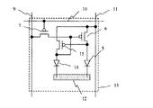
図5には、デジタルデータを画素に供給して、発光期間や発光強度を制御し、画素内でデジタルアナログ変換(DA変換)を行うデジタル駆動の画素回路が示されている。図5にはダイナミック回路でDA変換を行う画素(図5A)とスタティック回路で行う画素(図5B)が示されている。 FIG. 5 shows a digitally driven pixel circuit that supplies digital data to a pixel, controls a light emission period and light emission intensity, and performs digital analog conversion (DA conversion) in the pixel. FIG. 5 shows a pixel that performs DA conversion with a dynamic circuit (FIG. 5A) and a pixel that performs with a static circuit (FIG. 5B).
図5Aの画素回路13は、(第1)有機EL素子5、それを駆動する(第1)駆動トランジスタ6、ゲートライン10に選択電圧が印加されると、データライン9からのデジタルデータを画素内に取り込むゲートトランジスタ7、デジタルデータを保持する保持容量8から構成されている。有機EL素子5のカソードはカソード電極12、アノードは駆動トランジスタ6のドレイン端子に接続され、駆動トランジスタ6のソース端子は電源ライン11、ゲート端子は保持容量の一端とゲートトランジスタ7のソース端子へ接続されている。ゲートトランジスタ7のゲート端子はゲートライン10、ドレイン端子はデータライン9へ、また保持容量の他端は電源ライン11へ接続されている。
When a selection voltage is applied to the (first) organic EL element 5, the (first)
ゲートライン10に選択電圧が供給され、保持容量に駆動トランジスタ6をオンするのに十分低い電圧(Lowデータ)が供給されると、有機EL素子5に電源ライン11からカソード電極12へオン電流が流れ、有機EL素子5は発光する。駆動トランジスタ6がオフするのに十分高い電圧(Highデータ)が書き込まれれば有機EL素子5には電流は流れず、発光しない。デジタル駆動では、この発光期間を制御したり、発光面積や印加電圧などが異なる図5の画素を複数備えて多階調化が実現されるが、図5Aの画素では、保持容量8に書き込まれたデータは時間の経過に伴い変化するため、繰り返し一定周期でデータを書き込む必要がある。
When a selection voltage is supplied to the
図5Bの画素回路13では、図5Aの保持容量8が省略され、代わりに第2有機EL素子14、第2駆動トランジスタ15が導入されている。第2有機EL素子14のカソードはカソード電極12、アノードは第2駆動トランジスタ15のドレイン端子、及び第1駆動トランジスタのゲート端子とゲートトランジスタ7との接続点に接続され、第2駆動トランジスタ15のゲート端子は第1有機EL素子5と第1駆動トランジスタ6の接続点に、ソース端子は電源ライン11へ接続されている。
In the
図5Bの画素回路13では、書き込み選択電圧(より低いLow電圧)がゲートライン10へ供給され、デジタルデータが一度書き込まれると書き込まれたデータは維持されるため、図5Aと異なり一定周期で再度データを書き込む必要はない。例えばLowデータが書き込まれれば第1駆動トランジスタ6はオンし、第2駆動トランジスタ15はオフするが、第1駆動トランジスタ6のゲート端子は第2有機EL素子14のアノードに接続されているため、ゲートトランジスタ7がオフした後も第2有機EL素子14によりLow電圧が継続して印加され、第1有機EL素子5の発光状態が維持される。Highデータが書き込まれた場合でも第1駆動トランジスタ6はオフ、第2駆動トランジスタ15はオンし第2有機EL素子14に電流が流れて発光するが、第2有機EL素子14のアノード電圧が、ゲートトランジスタ7がオフした後も、第1駆動トランジスタ6のゲート電位をHighに維持するため、第1有機EL素子5の非発光状態が維持される。ただし、第2有機EL素子14の発光は配線メタルやブラックマトリクスなどで外部へ漏れないように遮光され、第2有機EL素子14の発光によるコントラストの低下は回避される。
In the
図5A,Bのような画素回路13を図6のように6ビット導入し、各メモリ画素13−0〜13−5の発光に寄与する有機EL素子5をその発光強度の比が1:2:4:8:16:32となるように形成すれば画素回路13においてDA変換することで6ビット階調を生成することができる。
The
図7には第1の表示デバイス1として、図5Bのスタティックメモリを含む画素回路13を単位画素としてアレイ状に配置したスタティック画素アレイ16、ゲートデコーダ17、データデコーダ18から構成される表示デバイスを、また第2の表示デバイス2として、図5Aのダイナミックメモリを含む画素回路13を単位画素としてアレイ状に配置したダイナミック画素アレイ19、ゲートドライバ20、データドライバ21から構成される表示デバイスを導入したデュアルサイド有機ELディスプレイ(デュアルディスプレイ装置)の表示システム例が示されている。
FIG. 7 shows a display device including a
第1の表示デバイス1は主にキーパッドによる操作を伴うインタラクティブな表示が多いことを想定しており、ユーザーのアクションによりトリガーされて映像の表示が更新されることから、定期的な更新処理の必要のないスタティック画素アレイを採用している。各スタティックメモリを含む画素回路13のデータを更新する場合、ゲートデコーダ17により該当するゲートライン10を選択し、データデコーダ18により該当するカラムのデータのみをデータライン9に供給し、更新の必要なメモリ画素のデータのみを書き換える。一定周期で画素データを更新する必要がないため、不要なデータ転送による消費電力を低減できる。
The
一方、第2の表示デバイスはテレビ映像などのように一定周期で送られてくる動画データを表示するため、定期的に画素データを書き換える。したがってダイナミックメモリを含む画素回路13で十分であり、シフトレジスタなどで構成されるゲートドライバ20やデータドライバ21を用いて順次送られてくる画素データをゲートラインの上から下まで一定周期で順次更新する。
On the other hand, the second display device periodically rewrites pixel data in order to display moving image data sent at a constant cycle such as a television image. Accordingly, the
第1の表示デバイス1にはあまり色純度は必要ないが、同じ映像が表示され続けるため焼きつきにくいほうがよい。また高解像度が望ましいであろう。第2の表示デバイス2は高色純度が必要であるが、映像が頻繁に変わるため焼きつきは比較的少ないと考えられる。これらの各表示デバイスに表示されるコンテンツの特徴を考慮すると、第1の表示デバイス1は高解像度化が容易で、比較的寿命の長い白色とカラーフィルタでフルカラー化する有機EL形成手段を採用し、第2の表示デバイス2は高色純度の発光特性が得られるR(赤)G(緑)B(青)の材料をそれぞれ形成する手段を適用するなど、異なる有機ELの形成方法をそれぞれに施してもよい。
Although the
白色とカラーフィルタでフルカラー化する場合、サブピクセルをRGBの3サブピクセルに加え、白色画素Wを追加した4サブピクセルとして、使用頻度の多い白色を1サブピクセルで生成できるようにすると、カラーフィルタでのロスが少ないため、低消費電力化に効果的である。LCDの場合にもRGBWのサブピクセル構成は効果的であるし、また色域を広げるために追加するサブピクセルは異なる色であってもよい。 In the case of full color with white and color filter, if the subpixel is added to 3 subpixels of RGB and white pixel W is added as 4 subpixels, white frequently used can be generated with 1 subpixel. This is effective in reducing power consumption. Also in the case of LCD, the RGBW sub-pixel configuration is effective, and the sub-pixels added to widen the color gamut may be different colors.
一方の表示デバイスが使用されている最中は、他方は非使用期間に入り、定電圧が印加され、劣化均一化処理がなされる。両面に有機ELを導入すると、焼きつきが懸念されるが、2枚に使用頻度が分散されるため、1枚あたりの焼きつきは単一の場合と比較して低減されるだけでなく、非使用期間に均一化処理を行う機会が増えるため、さらに焼きつきを低減できる。 While one display device is being used, the other enters a non-use period, a constant voltage is applied, and deterioration uniformization processing is performed. When organic EL is introduced on both sides, there is a concern about burn-in, but because the frequency of use is distributed between the two sheets, the burn-in per sheet is not only reduced compared to a single case, but also non- Since there are more opportunities to perform the equalization process during the period of use, burn-in can be further reduced.
均一化処理の間、ゲートライン10を順に選択するか、すべてのゲートライン10を同時に選択し、その間データライン9に同時にLowデータを供給すれば全画素の有機EL素子5は定電圧で点灯される。ゲートライン10を選択したまま、データライン9をLowからHighにすれば定電圧印加は解除され、これを長い周期で繰り返すと有機EL素子は点滅しながら劣化均一化処理がなされるし、短い周期で繰り返せば、中間調の表示で均一化処理がなされているように見える。点灯消灯のデューティ比を変えれば劣化均一化電流を可変することができるため、先に述べたように非使用期間の程度に応じて適応的に劣化均一化電流を制御できる。
During the equalization process, the gate lines 10 are sequentially selected or all the gate lines 10 are simultaneously selected, and if low data is simultaneously supplied to the
図6のように多ビットのメモリ画素13−0〜13−5を単位画素に導入すると信号処理回路3などにフレームメモリを導入しなくて済むため、低コスト化が可能となる。特に複数の表示デバイスを搭載するディスプレイは部品点数が多くなり、コストが高くなるため、低コスト化は重要である。デジタル駆動のよい点は低温ポリシリコンTFTなどの高速動作が可能なデバイスを効果的に利用できる点である。特に低温ポリシリコンTFTを用いるとゲートデコーダ17、データデコーダ18、ゲートドライバ20、データドライバ21などのデジタル回路をメモリ画素と同じ基板上に形成できるため、ドライバICを必要とせず、低コスト化に有利である。
If the multi-bit memory pixels 13-0 to 13-5 are introduced into the unit pixel as shown in FIG. 6, it is not necessary to introduce a frame memory into the
あるいは、いずれかの表示デバイスのみにドライバICを導入し、信号処理回路3とセレクタ4の機能を追加することで、フレームメモリなどのリソースを共有し、もう一方の表示デバイスを制御してもよい。これは片方がアナログ駆動でもう片方がデジタル駆動の場合に便利である。なぜならアナログ駆動の場合、DA変換回路をデータドライバ側に必要とするため、ドライバICとして実現するほうが容易であるからである。このドライバICに信号処理回路3とセレクタ4を導入して、もう一方の表示デバイスを制御できる手段を設ければ異なる信号を画素に供給する組み合わせでも低コストに実現できる。
Alternatively, by installing a driver IC only in one of the display devices and adding the functions of the
あるいは低温ポリシリコンTFTを用いたアナログ回路でDA変換を行うデータドライバを形成し、もう一方のデジタル駆動の表示デバイスにドライバICを搭載し、こちらに信号処理回路3、セレクタ4を内蔵して他方を制御してもよい。ただし、アナログ駆動時の有機ELの画素回路は図5Aに示されるように、駆動トランジスタ6を定電流源として用い、保持容量8にアナログ電圧を書き込み、有機EL素子5を電流駆動することになる。
Alternatively, a data driver for performing DA conversion is formed by an analog circuit using a low-temperature polysilicon TFT, a driver IC is mounted on the other digitally driven display device, and a
図1の携帯端末のようにより小型で精細度が求められる場合には図6のように1単位画素内に多ビットを導入することは困難である。その場合は1単位画素内の画素回路13を例えば1ビットにし、信号処理回路3か、もしくはデータデコーダ18とデータドライバ21をドライバICとして、そのドライバIC内にフレームメモリを導入して、サブフレームを用いて発光期間を制御することにより多階調化するほうがよい。表示デバイスの一つはサブフレームを用いたデジタル駆動で高精細化し、もう一方は1単位画素に多ビットを導入してメモリレスとし、低コスト化してもよい。
In the case where a small size and high definition are required as in the portable terminal of FIG. 1, it is difficult to introduce multiple bits in one unit pixel as shown in FIG. In that case, the
図5Bのスタティックメモリ画素は、データライン9をLowにプリチャージし、ゲートライン10に書き込み時とは異なる読み出し選択電圧(より高いLow電圧)を供給することで、第1駆動トランジスタ6のゲート端子に保持されているデータをデータライン9に読み出すことができる。第1駆動トランジスタ6のゲート端子にHighが保持されている際、第1駆動トランジスタ6がオフして、第2駆動トランジスタ15がオンしているが、ゲートトランジスタ7をより高い読み出し選択電圧でオンすることで、第2駆動トランジスタ15より高抵抗なオン抵抗でデータライン9と第1駆動トランジスタ6のゲート端子が接続されるため、電源ライン11から第2駆動トランジスタ15を介して、第1駆動トランジスタ6のゲート端子をHighに維持しながら電流が流れ、データライン9をLowからHighにチャージしてデータが読み出される。
The static memory pixel of FIG. 5B precharges the
第1駆動トランジスタ6のゲート端子にLowが保持されている場合には、第1駆動トランジスタ6はオン、第2駆動トランジスタ15はオフしているが、ゲートトランジスタ7をオンしてもデータライン9には変化がない。したがって一定時間経過後にデータライン9の電位を読み出すことで、LowのままであればLowデータ、Highに変化していればHighデータが保持されているものと判断する。
When Low is held at the gate terminal of the
図5Bのメモリ画素を導入するとデータを読み出せるため、外部のフレームメモリを省略できる。 When the memory pixel of FIG. 5B is introduced, data can be read out, so that an external frame memory can be omitted.
例えば、第1、第2の表示デバイス1、2として、両方に同じ単位画素数のスタティック画素アレイを導入すると、片方を表示に使用している際、もう片方をメモリデバイスとして用いることができる。そうすれば、例えばそれぞれ1単位画素に3ビットのメモリ画素を導入しているとすると、外部にメモリを導入しなくとも、表示に使われていないもう片方の3ビットのメモリ画素を用いて6ビット階調を表示できる。
For example, when a static pixel array having the same number of unit pixels is introduced as both the first and
片方がLCDの場合でも同様に、図5Bのメモリ画素によるスタティック画素アレイをメモリデバイスとして用いればフレームメモリの一部として動作させることで、LCDの表示に用いるフレームメモリの一部を削減することができるし、LCDの画素にスタティックメモリを導入して、有機ELの表示の際にそのメモリを表示メモリの一部として利用してもよい。 Similarly, when one of the LCDs is used, if the static pixel array including the memory pixels of FIG. 5B is used as a memory device, a part of the frame memory used for LCD display can be reduced by operating as a part of the frame memory. Alternatively, a static memory may be introduced into the LCD pixel, and the memory may be used as a part of the display memory when displaying the organic EL.
いずれの場合でも、スタティック画素アレイを表示デバイスとして用いず、情報を格納するメモリデバイスとして用いる場合、その情報によって、有機EL素子が発光するため、電力を消費するし、この不要な発光により、有機EL素子が劣化する。これを避けるため、有機EL素子に流れる電流をできる限り小さくする目的で、メモリデバイスとして用いる場合に限り、有機EL素子に印加する電圧を、メモリ画素として動作する最低のレベルまで下げて動作させることが望ましい。 In any case, when the static pixel array is not used as a display device but is used as a memory device for storing information, the organic EL element emits light according to the information, which consumes power. The EL element deteriorates. In order to avoid this, the voltage applied to the organic EL element should be lowered to the lowest level that operates as a memory pixel only when used as a memory device in order to reduce the current flowing through the organic EL element as much as possible. Is desirable.
図8には、デュアルサイド有機ELディスプレイモジュールの全体構成が示されている。従来では片面にトランジスタ及び有機EL素子が形成された表示デバイスガラス基板と、片面に乾燥剤用のポケットが設けられ、その中に乾燥剤が入れられた封止ガラス基板の2枚を張り合わせて、周辺をシールする形態が用いられていたが、これを応用することで両面に表示デバイスを備える場合でも適切に封止することができる。両面に乾燥剤用のポケットを設けた封止用ガラス基板22を用意し、両面の乾燥剤用ポケットに乾燥剤を入れ、表示デバイス1、2のガラス基板を封止ガラス基板22の両側から挟み込み合わせ、両方の周辺をシールすればガラス3枚で従来同様の封止効果が期待できる。その後、各表示デバイス1、2のガラス基板に映像信号や制御信号を供給するためのフレキケーブルを圧着すれば、図8のモジュールは完成する。
FIG. 8 shows the overall configuration of the dual-side organic EL display module. Conventionally, a display device glass substrate in which a transistor and an organic EL element are formed on one side, and a desiccant pocket provided on one side, and two sheets of a sealing glass substrate in which the desiccant is put are bonded together, Although the form which seals the periphery was used, even when it provides a display device on both surfaces by applying this, it can seal appropriately. Prepare a
表示デバイスとして有機ELを用いると1枚のガラス基板上に表示デバイスを形成できるため、モジュールを非常に薄くできる。図2のパーソナルモニターの場合も同様に作製できるため、デュアルサイド有機ELディスプレイが大型化してもその厚みを薄くすることができる。 When an organic EL is used as the display device, the display device can be formed on one glass substrate, so that the module can be made very thin. Since the personal monitor shown in FIG. 2 can be manufactured in the same manner, the thickness can be reduced even if the dual-side organic EL display is enlarged.
LCDでもバックライトを表と裏で共有し、薄いデュアルサイドLCD(デュアルディスプレイ装置)を形成可能であるが、共有されるバックライトの光の一部は使用されていない他方のLCDに使用されるため、シングルサイドの場合よりも明るくしなくてはならず、共有する効果が少ない。したがって、デュアルディスプレイ装置を構成するならばいずれかの表示デバイスに有機ELディスプレイを用いるとモジュールの厚みをより薄くすることができる。 The LCD can also share a backlight on the front and back, forming a thin dual-sided LCD (dual display device), but some of the light of the shared backlight is used for the other unused LCD Therefore, it must be brighter than the single-side case, and the sharing effect is less. Therefore, if an organic EL display is used for any display device as long as a dual display apparatus is configured, the thickness of the module can be further reduced.
以上説明してきた内容はガラス基板、プラスチック基板、あらゆる基板に対しても同様に適用可能であるし、画素回路を形成する半導体材料の種別にも依存しない。また表示デバイスが透過型、反射型かにも依存しない。 The contents described above can be similarly applied to glass substrates, plastic substrates, and all substrates, and do not depend on the type of semiconductor material forming the pixel circuit. It does not depend on whether the display device is a transmissive type or a reflective type.
また、デュアルディスプレイ装置を構成する際、表示デバイス同士を直接張り合わせて形成しなくともよく、間に放熱板や、駆動回路基板を介してモジュール化される形態であってもよい。 Further, when the dual display device is configured, the display devices do not have to be directly bonded to each other, and may be modularized via a heat sink or a drive circuit board.
1 第1の表示デバイス、2 第2の表示デバイス、3 信号処理回路、4 セレクタ、5 (第1)有機EL素子、6 (第1)駆動トランジスタ、7 ゲートトランジスタ、8 保持容量、9 データライン、10 ゲートライン、11 電源ライン、12 カソード電極、13 画素回路、14 第2有機EL素子、15 第2駆動トランジスタ、16 スタティック画素アレイ、17 ゲートデコーダ、18 データデコーダ、19 ダイナミック画素アレイ、20 ゲートドライバ、21 データドライバ、22 封止ガラス基板。
DESCRIPTION OF
Claims (15)
2つのディスプレイは、表示特性が異なり、映像信号の特性に応じてディスプレイを切り換えて使用できることを特徴とするデュアルディスプレイ装置。 A dual display device having two displays capable of displaying the same video signal,
A dual display device characterized in that the two displays have different display characteristics and can be used by switching between the displays according to the characteristics of the video signal.
前記2つのディスプレイは、表示面が外側となるように一体化されることで表裏の関係で形成されていることを特徴とするデュアルディスプレイ装置。 The dual display device according to claim 1,
The dual display device is characterized in that the two displays are formed in a front-back relationship by being integrated so that the display surface is on the outside.
自然画の映像信号表示に一方のディスプレイを使用し、コンピュータ画像に他方のディスプレイを使用することを特徴とするデュアルディスプレイ装置。 The dual display device according to claim 1 or 2,
A dual display device using one display for video signal display of a natural image and the other display for a computer image.
一方のディスプレイは、有機ELディスプレイであって、他方は液晶ディスプレイであることを特徴とするデュアルディスプレイ装置。 The dual display device according to any one of claims 1 to 3,
One display is an organic EL display, and the other is a liquid crystal display.
複数のボタンを有する操作部を一面側に有する本体部に対し折り畳み可能に取り付けられ、操作部が操作可能になるように開かれた場合に液晶ディスプレイが操作部側に位置してアクティブになり、
操作部を覆うように折り畳んだ場合に、有機ELディスプレイが外側となってアクティブになることを特徴とするデュアルディスプレイ装置。 The dual display device according to claim 4, wherein
When the operation part having a plurality of buttons is foldably attached to the main body part on one side, and the operation part is opened so that it can be operated, the liquid crystal display becomes active on the operation part side,
A dual display device, wherein the organic EL display becomes active when folded so as to cover the operation unit.
有機ELディスプレイのメニュー画面を液晶ディスプレイのメニュー画面に比べ、黒の多い輝度の低い画面にすることを特徴とするデュアルディスプレイ装置。 The dual display device according to claim 4 or 5,
A dual display device characterized in that the menu screen of the organic EL display is a screen with a lot of black and low brightness compared to the menu screen of the liquid crystal display.
前記一方のディスプレイと、前記他方のディスプレイは、解像度が異なることを特徴とするデュアルディスプレイ装置。 The dual display device according to any one of claims 1 to 3,
The dual display apparatus according to claim 1, wherein the one display and the other display have different resolutions.
前記一方のディスプレイと、前記他方のディスプレイは、カラー画素を構成するサブピクセル構成が異なることを特徴とするデュアルディスプレイ装置。 The dual display device according to claim 1,
2. The dual display apparatus according to claim 1, wherein the one display and the other display have different sub-pixel configurations constituting color pixels.
前記一方のディスプレイはデルタ配列タイプのディスプレイであり、前記他方のディスプレイはストライプ配列タイプのディスプレイであることを特徴とするデュアルディスプレイ装置。 The dual display device according to claim 1,
2. The dual display apparatus according to claim 1, wherein the one display is a delta arrangement type display, and the other display is a stripe arrangement type display.
2つのディスプレイの画素は、表示データを記憶するメモリとして利用可能であり、一方のディスプレイを表示に利用する際に他方のディスプレイの画素を表示データのメモリとして利用することを特徴とするデュアルディスプレイ装置。 A dual display device having two displays capable of displaying the same video signal,
The dual display device is characterized in that the pixels of the two displays can be used as a memory for storing display data, and when one of the displays is used for display, the pixel of the other display is used as a memory for the display data. .
2つのディスプレイは、有機ELディスプレイであることを特徴とするデュアルディスプレイ装置。 The dual display device according to claim 10, wherein
The dual display device is characterized in that the two displays are organic EL displays.
前記有機ELディスプレイの各画素には、スタティックメモリが設けられていることを特徴とするデュアルディスプレイ装置。 The dual display device according to claim 11, wherein
A dual display device, wherein each pixel of the organic EL display is provided with a static memory.
前記有機ELディスプレイの各画素は、一方のRGB画素がそれぞれ異なる有機EL材料で形成され、他方は白色有機EL材料とカラーフィルタで形成されていることを特徴とするデュアルディスプレイ装置。 The dual display device according to claim 11 or 12,
Each pixel of the organic EL display is a dual display device in which one RGB pixel is formed of a different organic EL material, and the other is formed of a white organic EL material and a color filter.
封止基板が両ディスプレイで共有されていることを特徴とするデュアルディスプレイ装置。 The dual display device according to any one of claims 11 to 13,
A dual display device, wherein a sealing substrate is shared by both displays.
前記メモリとして利用可能な画素は、表示メモリの一部として利用されている場合、表示時と異なる電圧で駆動されて低消費電力で動作することを特徴とするデュアルディスプレイ装置。 The dual display device according to any one of claims 10 to 14,
The dual display device, wherein the pixel that can be used as the memory is driven with a voltage different from that at the time of display and operates with low power consumption when used as a part of the display memory.
Priority Applications (2)
| Application Number | Priority Date | Filing Date | Title |
|---|---|---|---|
| JP2007193883A JP5270120B2 (en) | 2007-07-25 | 2007-07-25 | Dual display device |
| US12/169,689 US20090027306A1 (en) | 2007-07-25 | 2008-07-09 | Dual display apparatus |
Applications Claiming Priority (1)
| Application Number | Priority Date | Filing Date | Title |
|---|---|---|---|
| JP2007193883A JP5270120B2 (en) | 2007-07-25 | 2007-07-25 | Dual display device |
Related Child Applications (1)
| Application Number | Title | Priority Date | Filing Date |
|---|---|---|---|
| JP2012006186A Division JP2012118552A (en) | 2012-01-16 | 2012-01-16 | Dual display device |
Publications (2)
| Publication Number | Publication Date |
|---|---|
| JP2009031448A true JP2009031448A (en) | 2009-02-12 |
| JP5270120B2 JP5270120B2 (en) | 2013-08-21 |
Family
ID=40294855
Family Applications (1)
| Application Number | Title | Priority Date | Filing Date |
|---|---|---|---|
| JP2007193883A Active JP5270120B2 (en) | 2007-07-25 | 2007-07-25 | Dual display device |
Country Status (2)
| Country | Link |
|---|---|
| US (1) | US20090027306A1 (en) |
| JP (1) | JP5270120B2 (en) |
Cited By (4)
| Publication number | Priority date | Publication date | Assignee | Title |
|---|---|---|---|---|
| JP2012186659A (en) * | 2011-03-06 | 2012-09-27 | Sony Corp | Display system, display device, and repeating device |
| JP2013516660A (en) * | 2010-01-06 | 2013-05-13 | アップル インコーポレイテッド | Transparent electronic device |
| US9681121B2 (en) | 2012-01-11 | 2017-06-13 | Ultra-D Coöperatief U.A. | Mobile display device |
| WO2018174459A1 (en) * | 2017-03-24 | 2018-09-27 | 삼성전자주식회사 | Flexible display and electronic device including same |
Families Citing this family (13)
| Publication number | Priority date | Publication date | Assignee | Title |
|---|---|---|---|---|
| EP2287702B1 (en) * | 2009-08-17 | 2018-05-02 | Lg Electronics Inc. | Mobile terminal and display controlling method thereof |
| JP2011166691A (en) * | 2010-02-15 | 2011-08-25 | Toshiba Corp | Electronic device |
| CN102214415A (en) * | 2010-04-09 | 2011-10-12 | 宏碁股份有限公司 | Electronic device and method for selecting display device |
| CN105023550B (en) * | 2010-12-17 | 2017-07-11 | 杜比实验室特许公司 | N for wide colour gamut and high brightness is modulated |
| TWI543128B (en) * | 2012-03-19 | 2016-07-21 | 天鈺科技股份有限公司 | Electronic device |
| KR20150052650A (en) * | 2013-11-06 | 2015-05-14 | 삼성전자주식회사 | Apparatus and method for controlling power |
| JP6421920B2 (en) * | 2014-09-03 | 2018-11-14 | カシオ計算機株式会社 | Display device, display control method thereof, and control program |
| JP2017215833A (en) * | 2016-06-01 | 2017-12-07 | 株式会社リコー | Information processing system, information processing method, information processing device, and program |
| US10866615B1 (en) | 2017-08-16 | 2020-12-15 | Apple Inc. | Electronic devices with two-stage displays |
| US10690986B2 (en) | 2017-09-13 | 2020-06-23 | Apple Inc. | Electronic devices having electrically adjustable optical shutters |
| CN108492796A (en) * | 2018-03-30 | 2018-09-04 | 京东方科技集团股份有限公司 | A kind of switching control and display equipment |
| FR3081251B1 (en) | 2018-05-16 | 2020-06-05 | Microoled | DISPLAY DEVICE FOR PROCESSING A DOUBLE INPUT SIGNAL |
| US11043183B2 (en) * | 2019-05-23 | 2021-06-22 | Dell Products, L.P. | Mitigation of screen burn-in for a foldable IHS |
Citations (19)
| Publication number | Priority date | Publication date | Assignee | Title |
|---|---|---|---|---|
| JPH04291393A (en) * | 1991-03-20 | 1992-10-15 | Fujitsu Ltd | Liquid crystal display device and its control method |
| JPH08129359A (en) * | 1994-10-31 | 1996-05-21 | Tdk Corp | Electroluminescence display device |
| JP2001222256A (en) * | 1999-11-08 | 2001-08-17 | Semiconductor Energy Lab Co Ltd | Light emitting device |
| JP2002511608A (en) * | 1998-04-15 | 2002-04-16 | ケンブリッジ ディスプレイ テクノロジー リミテッド | Display control device with low power consumption mode |
| JP2002140052A (en) * | 2000-08-23 | 2002-05-17 | Semiconductor Energy Lab Co Ltd | Portable information device and its driving method |
| JP2002158757A (en) * | 2000-11-22 | 2002-05-31 | Mitsubishi Electric Corp | Portable phone |
| JP2002199078A (en) * | 2000-12-26 | 2002-07-12 | Toshiba Corp | Portable electronic unit and mobile radio telephone system |
| JP2002534717A (en) * | 1999-01-08 | 2002-10-15 | インテル・コーポレーション | Readable matrix addressable display system |
| JP2002304136A (en) * | 2001-01-17 | 2002-10-18 | Seiko Epson Corp | Electronic equipment provided with organic electroluminescence display |
| JP2003036054A (en) * | 2001-07-24 | 2003-02-07 | Toshiba Corp | Display device |
| JP2004014316A (en) * | 2002-06-07 | 2004-01-15 | Rohm Co Ltd | Double-sided display organic electroluminescent (el) display module and information terminal |
| JP2004021044A (en) * | 2002-06-18 | 2004-01-22 | Toyota Industries Corp | Display device |
| JP2004163601A (en) * | 2002-11-12 | 2004-06-10 | Seiko Epson Corp | Electrooptical device, method of driving electrooptical device, and electronic equipment |
| JP2004517363A (en) * | 2001-01-04 | 2004-06-10 | インターナショナル・ビジネス・マシーンズ・コーポレーション | Pixel circuit |
| JP2005038608A (en) * | 2003-05-16 | 2005-02-10 | Semiconductor Energy Lab Co Ltd | Display |
| JP2005038266A (en) * | 2003-07-17 | 2005-02-10 | Sony Corp | Notebook-sized personal computer |
| JP2005183006A (en) * | 2003-12-15 | 2005-07-07 | Semiconductor Energy Lab Co Ltd | Light-emitting device and electronic equipment |
| JP2006011387A (en) * | 2004-05-21 | 2006-01-12 | Semiconductor Energy Lab Co Ltd | Display device and electronic apparatus having the same |
| JP2006162708A (en) * | 2004-12-02 | 2006-06-22 | Sony Corp | Liquid crystal display device, liquid crystal driving method, and data recording and reproducing apparatus |
Family Cites Families (10)
| Publication number | Priority date | Publication date | Assignee | Title |
|---|---|---|---|---|
| US6069593A (en) * | 1998-02-24 | 2000-05-30 | Motorola, Inc. | Display carrier and electronic display control for multiple displays in a portable electronic device |
| US6987496B2 (en) * | 2000-08-18 | 2006-01-17 | Semiconductor Energy Laboratory Co., Ltd. | Electronic device and method of driving the same |
| JP3726900B2 (en) * | 2002-06-24 | 2005-12-14 | セイコーエプソン株式会社 | Display device and electronic apparatus equipped with the same |
| JP3726073B2 (en) * | 2002-07-01 | 2005-12-14 | シャープ株式会社 | Mobile terminal device |
| CN1319356C (en) * | 2003-04-24 | 2007-05-30 | 三星电子株式会社 | Device and method for using a rotating key and controlling a display in a mobile terminal |
| US8537081B2 (en) * | 2003-09-17 | 2013-09-17 | Hitachi Displays, Ltd. | Display apparatus and display control method |
| US20060066227A1 (en) * | 2004-09-24 | 2006-03-30 | Virnich James L | Electronic device with dual display arrangement |
| JP4770267B2 (en) * | 2005-05-23 | 2011-09-14 | セイコーエプソン株式会社 | Display method and display device |
| US7676242B2 (en) * | 2005-07-12 | 2010-03-09 | Microsoft Corporation | Compact and durable thin smartphone |
| TWI268737B (en) * | 2005-07-29 | 2006-12-11 | Au Optronics Corp | Full-color organic electroluminescence panel with high resolution |
-
2007
- 2007-07-25 JP JP2007193883A patent/JP5270120B2/en active Active
-
2008
- 2008-07-09 US US12/169,689 patent/US20090027306A1/en not_active Abandoned
Patent Citations (19)
| Publication number | Priority date | Publication date | Assignee | Title |
|---|---|---|---|---|
| JPH04291393A (en) * | 1991-03-20 | 1992-10-15 | Fujitsu Ltd | Liquid crystal display device and its control method |
| JPH08129359A (en) * | 1994-10-31 | 1996-05-21 | Tdk Corp | Electroluminescence display device |
| JP2002511608A (en) * | 1998-04-15 | 2002-04-16 | ケンブリッジ ディスプレイ テクノロジー リミテッド | Display control device with low power consumption mode |
| JP2002534717A (en) * | 1999-01-08 | 2002-10-15 | インテル・コーポレーション | Readable matrix addressable display system |
| JP2001222256A (en) * | 1999-11-08 | 2001-08-17 | Semiconductor Energy Lab Co Ltd | Light emitting device |
| JP2002140052A (en) * | 2000-08-23 | 2002-05-17 | Semiconductor Energy Lab Co Ltd | Portable information device and its driving method |
| JP2002158757A (en) * | 2000-11-22 | 2002-05-31 | Mitsubishi Electric Corp | Portable phone |
| JP2002199078A (en) * | 2000-12-26 | 2002-07-12 | Toshiba Corp | Portable electronic unit and mobile radio telephone system |
| JP2004517363A (en) * | 2001-01-04 | 2004-06-10 | インターナショナル・ビジネス・マシーンズ・コーポレーション | Pixel circuit |
| JP2002304136A (en) * | 2001-01-17 | 2002-10-18 | Seiko Epson Corp | Electronic equipment provided with organic electroluminescence display |
| JP2003036054A (en) * | 2001-07-24 | 2003-02-07 | Toshiba Corp | Display device |
| JP2004014316A (en) * | 2002-06-07 | 2004-01-15 | Rohm Co Ltd | Double-sided display organic electroluminescent (el) display module and information terminal |
| JP2004021044A (en) * | 2002-06-18 | 2004-01-22 | Toyota Industries Corp | Display device |
| JP2004163601A (en) * | 2002-11-12 | 2004-06-10 | Seiko Epson Corp | Electrooptical device, method of driving electrooptical device, and electronic equipment |
| JP2005038608A (en) * | 2003-05-16 | 2005-02-10 | Semiconductor Energy Lab Co Ltd | Display |
| JP2005038266A (en) * | 2003-07-17 | 2005-02-10 | Sony Corp | Notebook-sized personal computer |
| JP2005183006A (en) * | 2003-12-15 | 2005-07-07 | Semiconductor Energy Lab Co Ltd | Light-emitting device and electronic equipment |
| JP2006011387A (en) * | 2004-05-21 | 2006-01-12 | Semiconductor Energy Lab Co Ltd | Display device and electronic apparatus having the same |
| JP2006162708A (en) * | 2004-12-02 | 2006-06-22 | Sony Corp | Liquid crystal display device, liquid crystal driving method, and data recording and reproducing apparatus |
Cited By (12)
| Publication number | Priority date | Publication date | Assignee | Title |
|---|---|---|---|---|
| JP2013516660A (en) * | 2010-01-06 | 2013-05-13 | アップル インコーポレイテッド | Transparent electronic device |
| US8890771B2 (en) | 2010-01-06 | 2014-11-18 | Apple Inc. | Transparent electronic device |
| US9367093B2 (en) | 2010-01-06 | 2016-06-14 | Apple Inc. | Transparent electronic device |
| US9830844B2 (en) | 2010-01-06 | 2017-11-28 | Apple Inc. | Transparent electronic device |
| US10657857B2 (en) | 2010-01-06 | 2020-05-19 | Apple Inc. | Transparent electronic device |
| JP2012186659A (en) * | 2011-03-06 | 2012-09-27 | Sony Corp | Display system, display device, and repeating device |
| US9681121B2 (en) | 2012-01-11 | 2017-06-13 | Ultra-D Coöperatief U.A. | Mobile display device |
| US10225547B2 (en) | 2012-01-11 | 2019-03-05 | Ultra-D Coöperatief U.A. | Mobile display device |
| WO2018174459A1 (en) * | 2017-03-24 | 2018-09-27 | 삼성전자주식회사 | Flexible display and electronic device including same |
| KR20180108271A (en) * | 2017-03-24 | 2018-10-04 | 삼성전자주식회사 | Flexible display and electronic device having the same |
| US11024693B2 (en) | 2017-03-24 | 2021-06-01 | Samsung Electronics Co., Ltd. | Flexible display and electronic device including same |
| KR102360492B1 (en) | 2017-03-24 | 2022-02-09 | 삼성전자주식회사 | Flexible display and electronic device having the same |
Also Published As
| Publication number | Publication date |
|---|---|
| US20090027306A1 (en) | 2009-01-29 |
| JP5270120B2 (en) | 2013-08-21 |
Similar Documents
| Publication | Publication Date | Title |
|---|---|---|
| JP5270120B2 (en) | Dual display device | |
| US10546540B1 (en) | Displays with multiple scanning modes | |
| US8681140B2 (en) | Display device and electronic apparatus having the same | |
| KR101065321B1 (en) | Organic light emitting display device and driving method thereof | |
| JP2005326859A (en) | Method and system for driving dual display panels | |
| JP4633669B2 (en) | Liquid crystal display device and driving method thereof | |
| US8884996B2 (en) | Display device and electronic unit having a plurality of potential lines maintained at gray-scale potentials | |
| JP2006139278A (en) | Driving method for high frame rate display system | |
| US8669927B2 (en) | Liquid crystal display device and driving method thereof | |
| US11127335B2 (en) | Driving controller for displaying image using dither patterns and display device having the same | |
| JP2004226543A (en) | Display device | |
| JP4432694B2 (en) | Electro-optical device, driving method of electro-optical device, and electronic apparatus | |
| JP2008020573A (en) | Electro-optical device and electronic equipment | |
| JP5456298B2 (en) | OLED display device | |
| KR20070048852A (en) | Display apparatus having panel damage prevention function and pixel moving method thereof | |
| JP2012118552A (en) | Dual display device | |
| JP2004077742A (en) | Display device | |
| US20090033601A1 (en) | Organic light emitting display and its driving method | |
| KR20110046113A (en) | Organic electroluminescent device | |
| JP4633033B2 (en) | Liquid crystal display device and portable information device | |
| JP5206178B2 (en) | Video display device and electronic device | |
| KR100667544B1 (en) | Driving device and method of organic light emitting display | |
| KR20040067290A (en) | driving circuit of liquid crystal display device | |
| US20230389160A1 (en) | Display apparatus and method of controlling the same | |
| US20230230522A1 (en) | Display device |
Legal Events
| Date | Code | Title | Description |
|---|---|---|---|
| RD03 | Notification of appointment of power of attorney |
Free format text: JAPANESE INTERMEDIATE CODE: A7423 Effective date: 20100319 |
|
| RD04 | Notification of resignation of power of attorney |
Free format text: JAPANESE INTERMEDIATE CODE: A7424 Effective date: 20100419 |
|
| A711 | Notification of change in applicant |
Free format text: JAPANESE INTERMEDIATE CODE: A711 Effective date: 20100520 |
|
| A621 | Written request for application examination |
Free format text: JAPANESE INTERMEDIATE CODE: A621 Effective date: 20100723 |
|
| A977 | Report on retrieval |
Free format text: JAPANESE INTERMEDIATE CODE: A971007 Effective date: 20111020 |
|
| A131 | Notification of reasons for refusal |
Free format text: JAPANESE INTERMEDIATE CODE: A131 Effective date: 20111108 |
|
| A521 | Request for written amendment filed |
Free format text: JAPANESE INTERMEDIATE CODE: A523 Effective date: 20120116 |
|
| A131 | Notification of reasons for refusal |
Free format text: JAPANESE INTERMEDIATE CODE: A131 Effective date: 20120221 |
|
| A521 | Request for written amendment filed |
Free format text: JAPANESE INTERMEDIATE CODE: A523 Effective date: 20120410 |
|
| A131 | Notification of reasons for refusal |
Free format text: JAPANESE INTERMEDIATE CODE: A131 Effective date: 20120508 |
|
| A521 | Request for written amendment filed |
Free format text: JAPANESE INTERMEDIATE CODE: A523 Effective date: 20120719 |
|
| TRDD | Decision of grant or rejection written | ||
| A01 | Written decision to grant a patent or to grant a registration (utility model) |
Free format text: JAPANESE INTERMEDIATE CODE: A01 Effective date: 20130507 |
|
| A61 | First payment of annual fees (during grant procedure) |
Free format text: JAPANESE INTERMEDIATE CODE: A61 Effective date: 20130509 |
|
| R150 | Certificate of patent or registration of utility model |
Free format text: JAPANESE INTERMEDIATE CODE: R150 Ref document number: 5270120 Country of ref document: JP Free format text: JAPANESE INTERMEDIATE CODE: R150 |
|
| R250 | Receipt of annual fees |
Free format text: JAPANESE INTERMEDIATE CODE: R250 |
|
| R250 | Receipt of annual fees |
Free format text: JAPANESE INTERMEDIATE CODE: R250 |
|
| R250 | Receipt of annual fees |
Free format text: JAPANESE INTERMEDIATE CODE: R250 |
|
| R250 | Receipt of annual fees |
Free format text: JAPANESE INTERMEDIATE CODE: R250 |
|
| R250 | Receipt of annual fees |
Free format text: JAPANESE INTERMEDIATE CODE: R250 |
|
| R250 | Receipt of annual fees |
Free format text: JAPANESE INTERMEDIATE CODE: R250 |
|
| R250 | Receipt of annual fees |
Free format text: JAPANESE INTERMEDIATE CODE: R250 |
|
| R250 | Receipt of annual fees |
Free format text: JAPANESE INTERMEDIATE CODE: R250 |
|
| R250 | Receipt of annual fees |
Free format text: JAPANESE INTERMEDIATE CODE: R250 |