JP2004226543A - Display device - Google Patents
Display device Download PDFInfo
- Publication number
- JP2004226543A JP2004226543A JP2003012394A JP2003012394A JP2004226543A JP 2004226543 A JP2004226543 A JP 2004226543A JP 2003012394 A JP2003012394 A JP 2003012394A JP 2003012394 A JP2003012394 A JP 2003012394A JP 2004226543 A JP2004226543 A JP 2004226543A
- Authority
- JP
- Japan
- Prior art keywords
- power supply
- light emitting
- emitting element
- data signal
- driving
- Prior art date
- Legal status (The legal status is an assumption and is not a legal conclusion. Google has not performed a legal analysis and makes no representation as to the accuracy of the status listed.)
- Pending
Links
- 239000003990 capacitor Substances 0.000 claims abstract description 20
- 239000011159 matrix material Substances 0.000 claims description 33
- 238000000034 method Methods 0.000 claims description 28
- 239000010409 thin film Substances 0.000 claims description 23
- 230000008569 process Effects 0.000 claims description 12
- 229910021420 polycrystalline silicon Inorganic materials 0.000 claims description 11
- 239000003086 colorant Substances 0.000 claims description 5
- 230000015572 biosynthetic process Effects 0.000 claims 1
- 235000019557 luminance Nutrition 0.000 description 52
- 238000005401 electroluminescence Methods 0.000 description 35
- 238000010586 diagram Methods 0.000 description 22
- 239000010410 layer Substances 0.000 description 12
- 239000000758 substrate Substances 0.000 description 10
- 239000010408 film Substances 0.000 description 8
- 239000011521 glass Substances 0.000 description 7
- 239000002184 metal Substances 0.000 description 7
- 229910052751 metal Inorganic materials 0.000 description 7
- 230000007423 decrease Effects 0.000 description 6
- 239000000463 material Substances 0.000 description 6
- 230000008901 benefit Effects 0.000 description 5
- 239000011368 organic material Substances 0.000 description 4
- 230000009467 reduction Effects 0.000 description 4
- 230000005540 biological transmission Effects 0.000 description 3
- XUIMIQQOPSSXEZ-UHFFFAOYSA-N Silicon Chemical compound [Si] XUIMIQQOPSSXEZ-UHFFFAOYSA-N 0.000 description 2
- 230000008859 change Effects 0.000 description 2
- 230000000694 effects Effects 0.000 description 2
- 239000004973 liquid crystal related substance Substances 0.000 description 2
- 238000002161 passivation Methods 0.000 description 2
- 230000004044 response Effects 0.000 description 2
- 229910052710 silicon Inorganic materials 0.000 description 2
- 239000010703 silicon Substances 0.000 description 2
- 229910021417 amorphous silicon Inorganic materials 0.000 description 1
- 239000000470 constituent Substances 0.000 description 1
- 230000005684 electric field Effects 0.000 description 1
- 239000007772 electrode material Substances 0.000 description 1
- AMGQUBHHOARCQH-UHFFFAOYSA-N indium;oxotin Chemical compound [In].[Sn]=O AMGQUBHHOARCQH-UHFFFAOYSA-N 0.000 description 1
- 239000011229 interlayer Substances 0.000 description 1
- 230000004048 modification Effects 0.000 description 1
- 238000012986 modification Methods 0.000 description 1
- 239000000126 substance Substances 0.000 description 1
Images


Classifications
-
- H—ELECTRICITY
- H10—SEMICONDUCTOR DEVICES; ELECTRIC SOLID-STATE DEVICES NOT OTHERWISE PROVIDED FOR
- H10K—ORGANIC ELECTRIC SOLID-STATE DEVICES
- H10K59/00—Integrated devices, or assemblies of multiple devices, comprising at least one organic light-emitting element covered by group H10K50/00
- H10K59/10—OLED displays
- H10K59/12—Active-matrix OLED [AMOLED] displays
- H10K59/131—Interconnections, e.g. wiring lines or terminals
- H10K59/1315—Interconnections, e.g. wiring lines or terminals comprising structures specially adapted for lowering the resistance
-
- H—ELECTRICITY
- H10—SEMICONDUCTOR DEVICES; ELECTRIC SOLID-STATE DEVICES NOT OTHERWISE PROVIDED FOR
- H10K—ORGANIC ELECTRIC SOLID-STATE DEVICES
- H10K59/00—Integrated devices, or assemblies of multiple devices, comprising at least one organic light-emitting element covered by group H10K50/00
- H10K59/10—OLED displays
- H10K59/12—Active-matrix OLED [AMOLED] displays
-
- H—ELECTRICITY
- H10—SEMICONDUCTOR DEVICES; ELECTRIC SOLID-STATE DEVICES NOT OTHERWISE PROVIDED FOR
- H10K—ORGANIC ELECTRIC SOLID-STATE DEVICES
- H10K59/00—Integrated devices, or assemblies of multiple devices, comprising at least one organic light-emitting element covered by group H10K50/00
- H10K59/30—Devices specially adapted for multicolour light emission
- H10K59/35—Devices specially adapted for multicolour light emission comprising red-green-blue [RGB] subpixels
Abstract
Description
【0001】
【発明の属する技術分野】
本発明は、電流駆動型の発光素子等を備えた表示装置に関する。
【0002】
【従来の技術】
電流駆動型発光素子を備えたアクティブマトリクス型画像表示装置、例えば有機EL(Electro Luminescence)パネルは、所定の有機蛍光物質に電界をかけることにより発光する現象を利用したディスプレイである。
【0003】
この有機ELパネルは、液晶パネルなどの他のフラットパネルディスプレイと比較した場合に以下の利点を有する。第1に、有機ELパネルはその駆動電圧が10V程度以下でよい。第2に、有機ELパネルは自ら発光するためバックライトを必要としない。第3に、有機ELパネルはPDP(プラズマディスプレイパネル)などでは必要となる真空構造を必要としない。これらの利点から、有機ELパネルは小型かつ軽量に構成することができ、また低消費電力である。さらに第4に、有機ELパネルは応答速度が数μsecであり高速な応答性能を有する。第5に、有機ELパネルは視野角が170度以上であり広視野角を有する。近時、有機ELパネルは、これらの利点を生かして軽量の携帯機器向けディスプレイとするための開発が進められている。
【0004】
この有機ELパネルを例とする電流駆動型発光素子を備えたアクティブマトリクス型画像表示装置の駆動方式としては、単純マトリクス方式とアクティブマトリクス方式とが知られている。以下、アクティブマトリクス方式の画像表示装置について図を参照しつつ概説する。
【0005】
図9は、上記アクティブマトリクス型画像表示装置である有機ELパネルの一般的な画素形成部(説明の便宜のため、以下「画素」と略する)の構成を示す等価回路を示す図である。図9に示す画素は、電流駆動型発光素子3(以下「発光素子3」と略する)と、データ信号制御用スイッチング素子1(以下「スイッチング素子1」と略する)と、発光素子駆動用素子2(以下「駆動用素子2」と略する)と、補助容量4とを備えており、データ信号を与えるデータ信号線5(図中では「Data」とも表記する)と、走査信号与える走査信号線6(図中では「Sel」とも表記する)と、基準電圧を与える発光素子駆動用電源供給線7(以下「電源供給線7」と略し、図中では「Vref」とも表記する)とを配されている。なお、上記スイッチング素子1はNチャネルトランジスタであり、上記駆動用素子2はPチャネルトランジスタである。
【0006】
図9に示すように、データ信号線5と走査信号線6とは直交し、データ信号線5と電源供給線7とは平行するように配置される。また、スイッチング素子1のソースSにはデータ信号線5が接続され、そのゲートGには走査信号線6が接続され、そのドレインDには補助容量4の一端と駆動用素子2のゲートGとが接続される。補助容量4の他端は電源供給線7に接続される。駆動用素子2のソースSは電源供給線7に接続され、そのドレインDには発光素子3のアノードAが接続される。また、発光素子3のカソードCは、当該画素の上層に形成される金属製共通電極に接続される。
【0007】
さらに、この画素の動作について説明する。まず、走査信号線6の走査信号がアクティブであるとき、スイッチング素子1がオンされるため、データ信号線5に供給されるデータ信号値に対応する電荷がスイッチング素子1を介し、駆動用素子2のゲートに供給されるとともに補助容量4に供給および蓄積される。この駆動用素子2がオン状態のときには発光素子3に電流が流されるため発光素子3は発光する。次に、スイッチング素子1がオフされた後も、補助容量4に蓄積された電荷が保持される限り駆動用素子2のオン状態は継続するので、発光素子3は発光し続けることになる。
【0008】
この構成では、データ信号の電位をアナログ的に変化させ、駆動用素子2に流れる電流を制御することにより発光素子3の輝度を制御し、階調を表現することができる。このような階調表現方式は、アナログ階調方式と呼ばれる。しかし、この方式ではスイッチング素子1のオフ特性や、駆動用素子2の素子特性のバラツキなどに基づく各発光素子3の輝度のバラツキにより輝度ムラが生じやすい。このようなアナログ階調方式とは異なり、発光素子の発光時間を制御することにより階調を表現するデジタル階調方式と呼ばれるものがある。以下、図を参照して具体的に説明する。
【0009】
デジタル階調方式では、具体的には1フレーム(すなわち表示されるべき1枚の絵の表示期間)を複数のサブフレームに分割することにより、発光時間が制御される。図10は、64階調を表現する場合における、各サブフレームの発光期間を示す図である。図10に示すように、例えば64階調を表現する場合、サブフレームSF1〜SF6に含まれる期間であって、図中の斜線部分として示される各発光期間は、それぞれが1:2:4:8:16:32の比となるように設定される。なお、図中の空白部分として示されるアドレス期間は画素の選択が行われる期間であり、どのサブフレームにおいても一定の時間となる。このように、各サブフレーム内で1画面全てのアドレッシングが行われ、かつ発光素子の発光が行われる。図10に示す例では、1フレーム期間内に6回、上記動作が行なわれる。ここで例えば、15/64階調を表現する場合には、サブフレームSF1〜SF4の発光期間で発光させ、サブフレームSF5およびSF6の発光期間で消灯させることにより表現される。このデジタル階調方式では、発光素子3は完全なオン状態であるかまたは完全なオフ状態であるかの2値の状態しか取らないため、スイッチング素子1および駆動用素子2の素子特性のバラツキの影響を受けにくく輝度ムラが発生しにくいが、高速でアドレッシングを行なわなければならない。よって、データ信号線5には非常に速い伝送速度が要求される。
【0010】
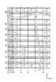
上記のように構成され動作する図9に示す画素の配列構成について説明する。図11は、上記画素を(m×RGB×n)個配列して構成されるアクティブマトリクス型画像表示装置である有機ELパネルの構成を示す模式図である。なお、ここでのRGBとは赤・緑・青の3色に対応する3個の画素を指す。よって、上記パネルは縦にn個、横に3m個の画素が配列されることになる。また、図中の点線で囲まれた領域は画素を示す。ここで、図11に示すRed用データ信号線DR1,DR2,DR3,…,DRmと、Green用データ信号線DG1,DG2,DG3,…,DGmと、Blue用データ信号線DB1,DB2,DB3,…,DBmとは、図9に示すデータ信号線5に対応し、図11に示す走査信号線S1,S2,S3,…,Snは、図9に示す走査信号線6に対応し、図11に示すRed用電源供給線VRと、Green用電源供給線VGと、Blue用電源供給線VBとは、図9に示す電源供給線7に対応する。また、図11の画素R(1,1)〜R(m,n)に含まれるRed用発光素子と、画素G(1,1)〜G(m,n)に含まれるGreen用発光素子と、画素B(1,1)〜B(m,n)に含まれるBlue用発光素子とは、図9に示す発光素子3に対応する。
【0011】
これらの画素R,G,Bでカラー表示が行われる場合、上記Red用発光素子とGreen用発光素子とBlue用発光素子とは、通常、それぞれを構成する材料に応じて素子特性が互いに異なる。例えばRed用発光素子により200cd/m2 の輝度を得るためには、駆動用素子が充分オンしているとき、Red用発光素子のアノードとカソードとの間に約12Vの電圧を印加する必要がある。これに対し、Green用発光素子により上記輝度を得るためには、駆動用素子が充分オンしているとき、Green用発光素子のアノードとカソードとの間に約8Vの電圧を印加する必要がある。したがって、同一の輝度を得るのに必要な電流を各発光素子の素子特性に応じて供給するため、図11に示すように、電源供給線7はRed用、Green用、およびBlue用の3種類を要するのが通常である。
【0012】
電源供給線7は各発光素子3に供給されるべき大きな電流を流すことが要求される。また、データ信号線5には速いデータ伝送速度が要求される。特に前述したデジタル階調方式の場合、データ信号線5には非常に速い伝送速度が要求される。このため、電源供給線7およびデータ信号線5の抵抗値は小さいことが望ましい。そこで通常、電源供給線7およびデータ信号線5はゲート電極の材料よりも抵抗率の小さい配線層材料で形成され、電源供給線7とデータ信号線5とは互いに平行するように配置される。
【0013】
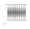
この電源供給線7に関して具体的に説明する。図12は、従来のアクティブマトリクス型画像表示装置である有機ELパネルに含まれる、片側入力方式(ここではパネル上部から電源を供給する方式)での電源供給線7の配置位置および電圧降下の状態を示す模式図である。また、図13は、両側入力方式(パネル上部および下部から電源を供給する方式)での電源供給線7の配置位置および電圧降下の状態を示す模式図である。ここで、例えば1画素を構成する発光素子3を発光させるためには1μAの電流が必要であるものとし、1本の電源供給線7が1ライン(図のY方向)に配列された100画素に電流を供給するものとする。この1ライン全ての画素が発光するとき、1本の電源供給線7には100μAが流れることになる。したがって、当該電源供給線7の配線抵抗が200Ωであるものとすると、図12に示す片側入力方式の電源供給線7では、当該電源供給線7の上端と下端との間で最大20.0mVの電圧降下が生じることになる。また、図13に示す両側入力方式の電源供給線7では、当該電源供給線7の中央部と上端または中央部と下端との間で最大10.0mVの電圧降下が生じることになる。これらの電圧降下の状態は、パネルの表示部分10に付されている色が濃いほど電圧が低いことを表すように模式的に図示されている。
【0014】
さらに、発光素子3はダイオード特性を有しているため、発光素子3に流れる電流は電圧の変化に対して指数関数的に変化することになる。ここで、発光素子3に流れる電流をIoledとし、発光素子3への印加電圧をVoledとすると、これらの関係は、次式(1)のように示される。なお、A、Bは定数であるものとする。
Ioled=A・{exp(B・Voled)−1} …(1)
また、発光素子3に流れる電流Ioledとその輝度とはほぼ比例関係にある。したがって、電源供給線7の配置方向に沿って(すなわち電流が供給される方向に)各画素の輝度が指数関数的に変化することにより、画像表示装置に顕著な輝度ムラが生じる。また、対応する電源供給線7から電流を供給されるRed用、Green用、およびBlue用の各発光素子3の素子特性が均一でなければ、流れる電流がそれぞれ異なるため、縞状の輝度ムラが発生する。このため、電源供給線7の抵抗値は小さいことが望ましい。
【0015】
【特許文献1】
特開2000−29419号公報
【特許文献2】
特開2000−187994号公報
【特許文献3】
特開平11−265166号公報
【0016】
【発明が解決しようとする課題】
このように、従来よりアクティブマトリクス型画像表示装置である有機ELパネルの構成および駆動方法には様々な態様がみられるが、ここでの発光素子は電流駆動型であるため、どのような構成においても発光素子に電流を供給するための電源供給線が不可欠である。ここで、全面点灯(電源供給線から電流が供給される1ライン全ての発光素子を点灯)した場合、電源供給線には上述した電圧降下が生じるため発光素子への印加電圧が変化し、この電圧変化がダイオード特性を有する発光素子の輝度に指数関数的な影響をあたえ、当該画像表示装置に顕著な輝度ムラを発生させていた。なお、このような輝度ムラは、1ラインの発光素子を多く点灯させた場合にも当然生じうる。また、上述のように発光色を異にする各発光素子の素子特性が均一でなければ縞状の輝度ムラが発生するため、電源供給線の抵抗値を小さくしなければならない。
【0017】
そこで、本発明の目的は、電源供給線の抵抗値を特に小さくすることなく発光素子の素子特性の相違による縞状の輝度ムラが防止される表示装置を提供することである。また、本発明の他の目的は、発光素子のダイオード特性に基づき電源供給線の延設方向に生じる顕著な輝度ムラが発生しない表示装置を提供することである。
【0018】
【課題を解決するための手段】
第1の発明は、電流により駆動される発光素子、当該発光素子に流れるべき電流を与える駆動用素子、および当該駆動用素子を制御するためのデータ信号を当該駆動用素子に与えるスイッチング素子を含む画素形成部をマトリクス状に複数配列してなる画素形成部群と、前記スイッチング素子を制御するための走査信号を前記スイッチング素子に与える走査信号線と、前記データ信号を前記スイッチング素子に与えるデータ信号線と、前記発光素子を駆動するための電流を前記駆動用素子に与える電源供給線とを備える表示装置であって、
前記電源供給線は、複数の縦方向電源供給線および複数の横方向電源供給線からなり、当該縦方向電源供給線および当該横方向電源供給線は、互いに交差するように格子状に配設され、交差点の少なくとも1つで電気的に接続されることを特徴とする。
【0019】
このような第1の発明によれば、格子状に配設される電源供給線により電圧降下の状態が2次元的に拡散されるため、電源供給線の延設方向に生じる輝度ムラが抑制される。
【0020】
第2の発明は、第1の発明において、
前記画素形成部群は、発光色を異にする複数の種類からなり、
前記縦方向電源供給線および前記横方向電源供給線は、前記画素形成部群の種類毎に独立して電流が供給されるように、前記画素形成部群の種類毎に配設されることを特徴とする。
【0021】
このような第2の発明によれば、発光色の異なる画素毎に独立して電流を供給するので、開口率低下を最小限に抑えながら、かつ輝度ムラが解消される。
【0022】
第3の発明は、電流により駆動される発光素子、当該発光素子に流れるべき電流を与える駆動用素子、当該駆動用素子を制御するためのデータ信号を当該駆動用素子に与えるスイッチング素子、および当該駆動用素子に与えられるデータ信号値に相当する電荷を蓄積する補助容量を含む画素形成部をマトリクス状に複数配列してなる画素形成部群と、前記スイッチング素子を制御するための走査信号を前記スイッチング素子に与える走査信号線と、前記データ信号を前記スイッチング素子に与えるデータ信号線と、前記発光素子を駆動するための電流を前記駆動用素子に与える電源供給線とを備える表示装置であって、
前記画素形成部群は、前記発光素子の素子特性を異にする複数の種類からなり、
前記補助容量の容量値は、当該画素形成部を構成する発光素子の素子特性に基づき設定されることを特徴とする。
【0023】
このような第3の発明によれば、発光素子の素子特性に対応して補助容量を異なる値に設定するので、各発光素子毎の素子特性が均一でない場合に発生する縞状の輝度ムラが抑制される。
【0024】
第4の発明は、電流により駆動される発光素子、当該発光素子に流れるべき電流を与える駆動用素子、および当該駆動用素子を制御するためのデータ信号を当該駆動用素子に与えるスイッチング素子を含む画素形成部をマトリクス状に複数配列してなる画素形成部群と、前記スイッチング素子を制御するための走査信号を前記スイッチング素子に与える走査信号線と、前記データ信号を前記スイッチング素子に与えるデータ信号線と、前記発光素子を駆動するための電流を前記駆動用素子に与える電源供給線とを備える表示装置であって、
前記画素形成部群は、前記発光素子の素子特性を異にする複数の種類からなり、
前記画素形成部の有効表示領域の大きさは、当該画素形成部を構成する発光素子の素子特性に基づき設定されることを特徴とする。
【0025】
このような第4の発明によれば、発光素子の素子特性に対応して有効表示領域の大きさが異なるので、各発光素子毎の素子特性が均一でない場合に発生する縞状の輝度ムラが抑制される。
【0026】
第5の発明は、第3または第4の発明において、
前記電源供給線は、複数の縦方向電源供給線および複数の横方向電源供給線からなり、当該縦方向電源供給線および当該横方向電源供給線は、互いに交差するように格子状に配設され、交差点の少なくとも1つで電気的に接続されることを特徴とする。
【0027】
このような第5の発明によれば、格子状に配設される電源供給線により電圧降下の状態が2次元的に拡散されるため、電源供給線の延設方向に生じる輝度ムラが抑制される。また、発光素子の素子特性に対応して補助容量値、もしくは、有効表示領域を異にしているため、独立に電流を供給することがなく、開口率低下を最小限に抑えながら、各発光素子毎の素子特性が均一でない場合に発生する縞状の輝度ムラが抑制される。
【0028】
第6の発明は、第1から第4までのいずれか1つの発明において、
前記スイッチング素子および前記駆動用素子は、薄膜トランジスタからなり、当該薄膜トランジスタおよび前記発光素子は、同一の工程で形成されることを特徴とする。
【0029】
このような第6の発明によれば、薄膜トランジスタと発光素子とを同一のプロセスで形成するため、画素や信号線等が同一基板上に形成される。
【0030】
第7の発明は、第1から第4までのいずれか1つの発明において、
前記スイッチング素子および前記駆動用素子は、600℃以下の低温プロセスで形成された多結晶シリコン薄膜トランジスタからなることを特徴とする。
【0031】
このような第7の発明によれば、600℃以下のプロセス温度で多結晶シリコン薄膜トランジスタを形成するので、安価で大型化が容易なガラスを基板として用いることができる。
【0032】
【発明の実施の形態】
以下、添付図面を参照して本発明の各実施形態について説明する。
【0033】
(第1の実施形態)
本実施形態に係る表示装置である電流駆動型発光素子を備えたアクティブマトリクス型画像表示装置(例えば有機ELパネル)の構造につき、図1を参照して説明する。図1は、本実施形態に係るアクティブマトリクス型画像表示装置である有機ELパネルの構造例を示す断面図である。図1に示すように ガラス基板111上には活性層となる多結晶のシリコン薄膜110が形成され、さらにゲート絶縁膜108を挟んでゲート電極109および層間絶縁膜107が形成される。その後、シリコン薄膜110が露出されるようにコンタクト部が開口され、当該コンタクト部に配線層105が形成される。さらにその上に不動態化するためのパッシベーション膜106と表面を平坦にするための平坦化膜104とが形成された後、配線層105が露出されるようにコンタクト部が開口される。この上に例えばITO(Indium Tin Oxide)からなる透明導電膜103が形成される。この透明導電膜103はアノード電極となる。さらに、その上に蛍光材料である有機材料102が塗布された後、共通電極としての金属製導電層101が形成される。この金属製導電層101はカソード電極となる。
【0034】
ここで、上記多結晶のシリコン薄膜110は、後述するデータ信号制御用スイッチング素子と発光素子駆動用素子とを構成する多結晶の薄膜トランジスタ(TFT:Thin Film Transistor)の主要な構成要素であり、この多結晶シリコン薄膜トランジスタと上記有機材料を含む発光素子とは同一の工程で形成される。この工程の詳細は、例えば特開2000−184994号公報や、特開2000−29419号公報において開示されているため、説明を省略する。この同一のプロセスで上記薄膜トランジスタと上記有機材料を含む発光素子とを形成することにより、画素(および関連する回路)を容易に同一基板上に形成することができる。また、多結晶シリコンは電子移動度が高いことから、データ信号制御用スイッチング素子および発光素子駆動用素子に上記多結晶シリコン薄膜トランジスタが用いられる構成は、例えば従来のアクティブマトリクス液晶表示装置に用いられていた非晶質シリコンの薄膜トランジスタが用いられる構成と比較して極めて高い駆動能力を得ることができる。また、上記多結晶シリコン薄膜トランジスタは、ガラス基板上に600℃以下のプロセスで形成されている構成である。このプロセスも上記公報において開示されているため、説明を省略する。この600℃以下のプロセス温度で多結晶シリコン薄膜トランジスタを形成する構成により、歪み点温度が低い反面、安価で大型化が容易なガラスを基板として用いることができ、大型の画像表示装置を低コストで製造することができる。
【0035】
また、上記有機ELパネル(の有機材料102)は、上記シリコン薄膜110を含む薄膜トランジスタが形成されるガラス基板111方向へ発光する。このような構造は順(スタガー)構造と呼ばれる。これに対して、アノード電極となる透明導電膜103とカソード電極となる金属製導電層101とを入れ替えることにより、上記方向とは逆の方向に発光させてもよい。この構造は逆(スタガー)構造と呼ばれる。なお、この逆構造は、TFTが形成されているガラス基板を光が通過しない構造であるため開口率を大きくすることができるという利点を有するが、金属製導電層上に有機膜を形成することが困難であるという欠点を有するため、通常は順構造が好適である。
【0036】
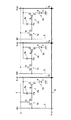
ここで、本実施形態に係る表示装置である有機ELパネルの画素の構成および動作について説明する。図2は当該画素の等価回路を示す回路図である。図2に示す画素は、図9に示す従来の画素と同様に、電流駆動型発光素子3(以下「発光素子3」と略する)と、データ信号制御用スイッチング素子1(以下「スイッチング素子1」と略する)と、発光素子駆動用素子2(以下「駆動用素子2」と略する)と、補助容量4とを備えており、データ信号を与えるデータ信号線5(図中では「Data」とも表記する)と、走査信号を与える走査信号線6(図中では「Sel」とも表記する)とを配されており、さらに図9に示す従来の画素とは異なり、基準電圧を与える2本の発光素子駆動用電源供給線7a,7b(以下「電源供給線7a,7b」または単に「電源供給線7」と略し、図中では「Vref」とも表記する)を配されている。なお、上記スイッチング素子1はNチャネルトランジスタであり、上記駆動用素子2はPチャネルトランジスタである。
【0037】
図2に示すように、データ信号線5と走査信号線6とは直交し、データ信号線5と電源供給線7aとは平行するように配置される。さらに、電源供給線7aと電源供給線7bとは直交するように配置され、その交差点で互いに接続される。また、スイッチング素子1のソースSにはデータ信号線5が接続され、そのゲートGには走査信号線6が接続され、そのドレインDには補助容量4の一端と駆動用素子2のゲートGとが接続される。補助容量4の他端は電源供給線7aに接続される。駆動用素子2のソースSは電源供給線7aに接続され、そのドレインDには発光素子3のアノードAが接続される。また、発光素子3のカソードCは、図1に示されるように当該画素の上層に形成される金属製共通電極に接続される。
【0038】
さらに、この画素の動作について説明する。まず、走査信号線6の走査信号がアクティブであるとき、スイッチング素子1がオンされるため、データ信号線5に供給されるデータ信号値に対応する電荷がスイッチング素子1を介し、駆動用素子2のゲートに供給されるとともに補助容量4に供給および蓄積される。この駆動用素子2がオン状態のときには発光素子3に電流が流されるため発光素子3が発光する。次に、スイッチング素子1がオフされた後も、補助容量4に蓄積された電荷が保持される限り駆動用素子2のオン状態は継続するので、発光素子3は発光し続けることになる。
【0039】
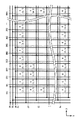
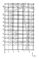
この図2に示す画素の配列構成について説明する。図3は、上記画素を((m×RGB)×n)個配列して構成されるアクティブマトリクス型画像表示装置である有機ELパネルの構成を示す模式図である。なお、ここでのRGBとは赤・緑・青の3色の画素に対応する3個の画素を指す。よって、上記パネルでは縦にn個、横に3m個の画素が配列されることになる。また、図中の点線で囲まれた領域は画素を示す。ここで、図3に示すRed用データ信号線DR1,DR2,DR3,…,DRmと、Green用データ信号線DG1,DG2,DG3,…,DGmと、Blue用データ信号線DB1,DB2,DB3,…,DBmとは、図2に示すデータ信号線5に対応し、図に示す走査信号線S1,S2,S3,…,Snは、図2に示す走査信号線6に対応し、図3に示すようにX方向およびY方向にそれぞれ配設されたRed用電源供給線VRと、Green用電源供給線VGと、Blue用電源供給線VBとは、図2に示す電源供給線7a,7bに対応する。また、図3の画素R(1,1)〜R(m,n)に含まれるRed用発光素子と、画素G(1,1)〜G(m,n)に含まれるGreen用発光素子と、画素B(1,1)〜B(m,n)に含まれるBlue用発光素子とは、図2に示す発光素子3に対応する。
【0040】
ここで、走査信号線S1に対応してこれと平行にX方向に延びるように配設された電源供給線VRと、走査信号線S2に対応してこれと平行にX方向に延びるように配設された電源供給線VGと、走査信号線S3に対応してこれと平行にX方向に延びるように配設された電源供給線VBとを1組として、この組がY方向に複数(具体的にはn/3)組繰り返されるように各走査信号線と平行に各電源供給線が配設される。また、データ信号線DR1に対応してこれと平行にY方向に延びるように配設された電源供給線VRと、データ信号線DG1に対応してこれと平行にY方向に延びるように配設された電源供給線VGと、データ信号線DB1に対応してこれと平行にY方向に延びるように配設された電源供給線VBとを1組として、この組がX方向に複数(具体的にはm)組繰り返されるように各データ信号線と平行に各電源供給線が配設される。なお、電源供給線VR,VG,VBは、それぞれの位置が入れ替えられてもよい。これらのX方向およびY方向に延びるように配設された電源供給線VRは、画素R(1,1)〜R(m,n)内の交差点で接続される。同様に、X方向およびY方向に延びるように配設された電源供給線VGは、画素G(1,1)〜G(m,n)内の交差点で接続され、X方向およびY方向に延びるように配設された電源供給線VBは、画素B(1,1)〜B(m,n)内の交差点で接続される。なお、これらの電源供給線は上記交差点全てにおいて接続されるのが好適であるが、これに限定されるわけではなく、交差点の1つ以上で接続される構成でもよい。
【0041】
この表示装置では、順構造の場合、X方向に配設される電源供給線VR,VG,VBのうち2つまたは全てが1画素内に配設される構成でもよい。しかし、この構成では開口率が著しく低下してしまうので、順構造の場合の開口率低下を最小限に抑えながら、かつ輝度ムラを解消するためには、図3に示す上記配置構成が最も効率の良い構成である。
【0042】
また、X方向に配置された電源供給線7bは、例えばゲート電極の材料のみにより構成されても良いし、配線層材料により構成され、Y方向に配置された電源供給線7aと交差する箇所にゲート電極材料を配しコンタクトを介して互いに接続されてもよい。このように構成すれば、本表示装置において電源供給線をX方向およびY方向に延びるように配設することができる。
【0043】
この電源供給線7a,7bの構成により、図12に示す従来の片側入力方式での電圧降下の状態や、図13に示す従来の両側入力方式での電圧降下の状態とは異なり、ここでの電圧降下の状態は2次元的に拡散された状態となる。すなわち、従来のY方向に配設される電源供給線7aに対してさらにX方向に追加される電源供給線7bからも電流が供給されることにより電圧降下が小さくなるとともに、電圧降下の状態すなわち同電位点の分布パターンが2次元的な広がりを有することになる。その結果、図12および図13に示す従来のY方向に変化する輝度ムラが抑制される。また、電源供給線VR,VG,VBがそれぞれ設けられる構成により、各画素R,G,Bに含まれる各発光素子毎の素子特性が均一でない場合にも各画素R,G,Bの輝度が均一になるように各発光素子毎に異なる適宜の電圧を印加することができるため、発生する縞状の輝度ムラが抑制される。さらに、X方向に配設される電源供給線VR,VG,VBのうちの1つのみが1画素内に配設される構成により、開口率低下が最小限に抑制されつつ輝度ムラが抑制される。
【0044】
なお、上記電源供給線VR,VG,VBは、表示装置上部から電源を供給するとともに、表示装置左側から電源を供給する片側入力構成であるが、両側入力構成であってもよい。すなわち、表示装置上部から電源が供給されるとともに下部からも電源が供給される構成でもよいし、表示装置左側から電源が供給されるとともに右側からも電源が供給される構成でもよいし、これら双方の構成を含んでもよい。
【0045】
(第2の実施形態)
本実施形態に係る表示装置である電流駆動型発光素子を備えたアクティブマトリクス型画像表示装置(例えば有機ELパネル)の全体的な構造は、後述する画素の構成および動作を除き、第1の実施形態の図1に示す全体的な構造と同様であるので説明を省略する。なお、本アクティブマトリクス型画像表示装置の全体構造は順(スタガー)構造のみならず、逆(スタガー)構造であってもよいことも第1の実施形態と同様である。
【0046】
次に、本実施形態に係る表示装置である有機ELパネルの画素の構成および動作について説明する。図4は当該画素の等価回路を示す回路図である。図4に示す3つの画素(画素R、画素G、および画素B)は、図2に示す第1の実施形態における画素と同様に、電流駆動型発光素子3a〜3c(以下「発光素子3a〜3c」と略する)と、データ信号制御用スイッチング素子1a〜1c(以下「スイッチング素子1a〜1c」と略する)と、発光素子駆動用素子2a〜2c(以下「駆動用素子2a〜2c」と略する)と、補助容量4a〜4cとを備えており、データ信号を与えるデータ信号線5(図中では「Data」とも表記する)と、走査信号を与える走査信号線6(図中では「Sel」とも表記する)と、基準電圧を与える2本の発光素子駆動用電源供給線7a,7b(以下「電源供給線7a,7b」または単に「電源供給線7」と略し、図中では「Vrgb」とも表記する)とを配されている。ここで、補助容量4a〜4cの容量値Ca,Cb,Ccは、Ca>Cb>Ccであり、前述した従来例の場合と同様に発光素子3a〜3cの素子特性がそれぞれ異なり、同一輝度を同一素子面積で得るために必要な発光素子3a〜3cへの供給電流Ir,Ig,Ibおよび印加電圧Vr,Vg,Vbは、Ir>Ig>IbであってかつVr>Vg>Vbであるものとする。但し、スイッチング素子1a〜1cのリーク電流はそれぞれ同一であるものとする。なお、上記スイッチング素子1a〜1cはNチャネルトランジスタであり、上記駆動用素子2a〜2cはPチャネルトランジスタである。
【0047】
図4に示すように、データ信号線5と走査信号線6とは直交し、データ信号線5と電源供給線7aとは平行するように配置される。さらに、電源供給線7aと電源供給線7bとは直交するように配置され、その交差点で互いに接続される。このように、画素R、画素G、および画素Bに対応する電源供給線7が共通となる点は、図2に示す第1の実施形態における画素と異なる。図5は、本実施形態における上記画素を((m×RGB)×n)個配列して構成されるアクティブマトリクス型画像表示装置である有機ELパネルの構成を示す模式図である。図5に示すように、電源供給線7に対応する電源供給線Vrgbが共通となる点が図3の場合とは異なるが、そのほかの配置構成は同様であるため、説明を省略する。再び図4を参照すると、スイッチング素子1a〜1cのソースSにはデータ信号線5が接続され、そのゲートGには走査信号線6が接続され、そのドレインDには補助容量4a〜4cの対応する一端と駆動用素子2a〜2cの対応するゲートGとが接続される。補助容量4a〜4cの他端は電源供給線7aに接続される。駆動用素子2a〜2cのソースSは電源供給線7aに接続され、その対応するドレインDには発光素子3a〜3cの対応するアノードAが接続される。また、発光素子3a〜3cのカソードCは、図1に示されるように当該画素の上層に形成される金属製共通電極に接続される。
【0048】
次に、画素R、画素G、および画素Bの動作について説明する。まず、走査信号線6の走査信号がアクティブであるとき、スイッチング素子1a〜1cがオンされるため、データ信号線5に供給されるデータ信号値に対応する電荷がスイッチング素子1a〜1cを介し、駆動用素子2a〜2cのゲートに供給されるとともに補助容量4a〜4cに供給および蓄積される。この駆動用素子2a〜2cがオン状態のときには発光素子3に電流が流されるため発光素子3が発光する。次に、スイッチング素子1a〜1cがオフされた後も、補助容量4a〜4cに蓄積された電荷が保持される限り駆動用素子2a〜2cのオン状態は継続するので、発光素子3a〜4cは発光し続けることになる。しかし、スイッチング素子1a〜1cの(ソース端子とドレイン端子との間の)リーク電流により、補助容量4a〜4cに蓄積された電荷量は徐々に減少する。ここで、上述のように補助容量4a〜4cの容量値Ca,Cb,Ccはそれぞれ異なるため、駆動用素子2a〜2cがオンするための閾値である所定の電位に達する時間がそれぞれ異なる。その結果、発光素子3a〜4cの発光期間がそれぞれ異なることになる。
【0049】
図6は、上記の画素R、画素G、および画素Bの動作を説明するための図である。図6に示すように、画素R、画素G、および画素Bに対応するデータ信号のアクティブ期間(またはアクティブ期間に相当する期間)は時刻t1から時刻t4までで同じであっても、対応する補助容量が異なるため発光素子の発光期間が異なる。ここで駆動用素子2a〜2cがオンするための閾値である所定の閾電位Vshが同じである場合、画素Rに対応する補助容量4aの容量値Caは大きいため、駆動用素子2aのゲート電位は急激に低下することはなく、時刻t4においても閾電位Vshよりも高い電位である。よって、発光素子3aは時刻t1から時刻t4まで発光し続ける。これに対し、画素Gに対応する補助容量4bの容量値Cbは中程度の大きさであるため、駆動用素子2bのゲート電位はやや早く低下し、時刻t3において閾電位Vshに達する。よって、発光素子3bは時刻t1から時刻t3まで発光し続ける。また、画素Bに対応する補助容量4cの容量値Ccは小さいため、駆動用素子2cのゲート電位は急激に低下し、時刻t2において閾電位Vshに達する。よって、発光素子3cは時刻t1から時刻t2まで発光し続ける。
【0050】
このように、駆動用素子2a〜2cのオン時間は、補助容量4a〜4cの容量値Ca〜Ccに基づき所望の時間に設定することができる。そのため、これらの容量値Ca〜Ccを異なる所定の値に設定することにより各発光素子3a〜3cの発光期間に所定の重み付けを行うことができる。したがって、発光素子3a〜3cの素子特性がそれぞれ異なるため、同一輝度を同一素子面積で得るために発光素子3a〜3cに供給しなければならない電流および印加電圧が異なる場合であっても、発光素子3a〜3cの発光期間に素子特性に応じた所定の重み付けを行うことにより、各画素をマトリクス状に配置し電源供給線7を共通化しつつ(図5に示す電源供給線Vrgb)、各画素R,G,Bに含まれる各発光素子毎の素子特性が均一でない場合に発生する縞状の輝度ムラが抑制される。すなわち、データ信号のアクティブ期間内での各画素R,G,Bの平均輝度がほぼ等しくなるよう、補助容量4a〜4cの容量値Ca〜Ccを素子特性に応じた所定の値に設定する。そうすれば、各発光素子3a〜3cの発光期間には素子特性に応じた所定の重み付けが行われるため、上記縞状の輝度ムラが抑制される。また、電源供給線7a,7bの構成により、第1の実施形態と同様に電圧降下の状態すなわち同電位点の分布パターンが2次元的な広がりを有することになるため、図12および図13に示す従来のY方向に変化する輝度ムラが抑制される。さらに、電源供給線Vrgbが共通化されるため、開口率低下が最小限に抑制されつつ輝度ムラが抑制される。
【0051】
なお、上記電源供給線Vrgbは、表示装置上部から電源を供給するとともに、表示装置左側から電源を供給する片側入力構成であるが、両側入力構成であってもよい。すなわち、表示装置上部から電源が供給されるとともに下部からも電源が供給される構成でもよいし、表示装置左側から電源が供給されるとともに右側からも電源が供給される構成でもよいし、これら双方の構成を含んでもよい。
【0052】
(第3の実施形態)
本実施形態に係る表示装置である電流駆動型発光素子を備えたアクティブマトリクス型画像表示装置(例えば有機ELパネル)の全体的な構造は、第1および第2の実施形態(の図1に示す全体的な構造)と同様であるので説明を省略する。なお、本アクティブマトリクス型画像表示装置の全体構造は順(スタガー)構造のみならず、逆(スタガー)構造であってもよいことも第1および第2の実施形態と同様である。
【0053】
次に、本実施形態に係る表示装置である有機ELパネルの画素の構成および動作について説明する。図7は当該画素の等価回路を示す回路図である。図7に示す3つの画素(画素R、画素G、および画素B)は、補助容量4a〜4cの容量値が同一であり、発光素子3a〜3cの発光面積(すなわち画素の有効表示領域)がそれぞれ異なる他は、図4に示す第2の実施形態における画素と同様であるため、説明を省略する。また、本実施形態における上記画素を((m×RGB)×n)個配列して構成されるアクティブマトリクス型画像表示装置である有機ELパネルの構成も、画素R、画素G、および画素Bに対応する電源供給線7が共通であるため図4に示す第2の実施形態と同様であり、説明を省略する。ここで、発光素子3a〜3cの発光面積Aa,Ab,Acは、Aa>Ab>Acであり、前述した従来例の場合と同様に発光素子3a〜3cの素子特性がそれぞれ異なり、同一輝度を同一素子面積で得るために必要な発光素子3a〜3cへの供給電流Ir,Ig,Ibおよび印加電圧Vr,Vg,Vbは、Ir>Ig>IbであってかつVr>Vg>Vbであるものとする。なお、上記スイッチング素子1a〜1cはNチャネルトランジスタであり、上記駆動用素子2a〜2cはPチャネルトランジスタである。
【0054】
画素R、画素G、および画素Bの動作については、第1の実施形態と同様であるため説明を省略する。ただし、上述のように発光素子3a〜3cの発光面積Aa,Ab,Acは異なるため、発光素子3a〜3cに対してそれぞれ上記電流Ir,Ig,Ibが流され上記印加電圧Vr,Vg,Vbが加えられる場合であっても、発光素子3a〜3cを含む画素R、画素G、および画素Bの輝度がそれぞれ異なることになる。ここで、本実施形態において画素R、画素G、および画素Bの輝度とは画素全体の面積を基準とする画素の平均輝度を意味するものとする。よって、各画素の輝度を異なるように構成するためには、これらの画素の有効表示領域がそれぞれ異なるように構成すれば足りるため、発光素子3a〜3cの発光面積が同一である構成も考えられる。
【0055】
図8は、同一輝度を同一素子面積で得るために必要な上記供給電流Ir,Ig,Ibおよび上記印加電圧Vr,Vg,Vbが与えられる場合における画素R、画素G、および画素Bの輝度の差異を説明するための図である。図8に示すように、画素R、画素G、および画素Bに対応するデータ信号のアクティブ期間(またはアクティブ期間に相当する期間)は時刻t1から時刻t4までであって同じであり、データ信号の振幅も同じであるが、対応する発光素子の発光面積が異なるため、各画素の(平均)輝度が異なる。例えば、画素Rに対応する発光素子3aの発光面積は大きいため、発光素子3aの発光期間が他の発光素子3b,3cと同じ時刻t1から時刻t4まででであっても、画素Rの輝度Baは画素Gの輝度Bbや画素Bの輝度Bcよりも大きい。また、画素Bに対応する発光素子3cの発光面積は小さいため、発光期間が同じであっても画素Bの輝度Bcは画素Rの輝度Baおよび画素Gの輝度Bbよりも小さい。
【0056】
このように、画素R、画素G、および画素Bは、発光素子3a〜3cの発光面積Aa,Ab,Acに基づき所望の輝度に設定することができる。したがって、発光素子3a〜3cの素子特性がそれぞれ異なるため、同一輝度を同一素子面積で得るために必要な発光素子3a〜3cに供給しなければならない電流および印加電圧が異なる場合であっても、発光素子3a〜3cの発光面積に素子特性に応じた所定の重み付けを行うことにより、各画素をマトリクス状に配置し電源供給線7を共通化しつつ(図7に示す電源供給線Vrgb)、各画素R,G,Bに含まれる各発光素子毎の素子特性が均一でない場合に発生する縞状の輝度ムラが抑制される。すなわち、ほぼ同一の電流および印加電圧が与えられる各画素R,G,Bの輝度がほぼ等しくなるよう、発光面積Aa,Ab,Acを素子特性に応じた異なる所定の大きさに設定する。このことにより、上記縞状の輝度ムラが抑制される。また、電源供給線7a,7bの構成により、第1の実施形態と同様に電圧降下の状態すなわち同電位点の分布パターンが2次元的な広がりを有することになるため、図12および図13に示す従来のY方向に変化する輝度ムラが抑制される。さらに、電源供給線Vrgbが共通化されるため、開口率低下が最小限に抑制されつつ輝度ムラが抑制される。
【0057】
なお、上記電源供給線Vrgbは、表示装置上部から電源を供給するとともに、表示装置左側から電源を供給する片側入力構成であるが、両側入力構成であってもよい。すなわち、表示装置上部から電源が供給されるとともに下部からも電源が供給される構成でもよいし、表示装置左側から電源が供給されるとともに右側からも電源が供給される構成でもよいし、これら双方の構成を含んでもよい。
【0058】
(変形例)
上記第1から第3までの各実施形態に係る表示装置である電流駆動型発光素子を備えたアクティブマトリクス型画像表示装置としては、有機ELパネルが例示されているが、FED(Field Emission Device)素子等の電流駆動型の発光素子が用いられてもよい。また、上記スイッチング素子および上記駆動用素子の一方または双方は、複数のトランジスタにより構成されてもよい。
【0059】
上記第1から第3までの各実施形態に係る表示装置は画素R,G,Bの3種類を含むが、画素の種類や数に限定はない。例えば画素が一種類のみであってもよいし、画素の種類が複数ある場合であっても当該画素に含まれる発光素子の素子特性がほぼ同一であってもよい。これらの場合、各発光素子の素子特性の差異を考慮する必要はなくなるため、画素の種類に対応する電源供給線の配線や、補助容量または発光素子の発光面積への重み付けは不要となるが、電源供給線をX方向およびY方向に配設する構成により、電圧降下の状態が2次元的に拡散されるため、図12および図13に示す従来のY方向に変化する輝度ムラを抑制することができる。
【0060】
【発明の効果】
第1の発明によれば、電源供給線を格子状に配設する構成により、電圧降下の状態が2次元的に拡散される。そのため、発光素子のダイオード特性に基づき電源供給線の延設方向に生じる輝度ムラを抑制することができる。
【0061】
第2の発明によれば、発光色の異なる3種類の画素毎に独立して電流を供給する構成により、順構造の場合の開口率低下を最小限に抑えながら、かつ輝度ムラを解消することができる。
【0062】
第3の発明によれば、発光素子の素子特性に対応して補助容量を異なる値に設定する構成により、各発光素子毎の素子特性が均一でない場合に発生する縞状の輝度ムラを抑制することができる。
【0063】
第4の発明によれば、発光素子の素子特性に対応して有効表示領域の大きさが異なる構成により、各発光素子毎の素子特性が均一でない場合に発生する縞状の輝度ムラを抑制することができる。
【0064】
第5の発明によれば、第1の発明と同様に電源供給線を格子状に配設する構成により、電圧降下の状態が2次元的に拡散される。そのため、発光素子のダイオード特性に基づき電源供給線の延設方向に生じる輝度ムラを抑制することができる。また、発光素子の素子特性に対応して補助容量値、もしくは、有効表示領域を異にしているため、独立に電流を供給することがなく、開口率低下を最小限に抑えながら、各発光素子毎の素子特性が均一でない場合に発生する縞状の輝度ムラが抑制される。
【0065】
第6の発明によれば、薄膜トランジスタと発光素子とを同一のプロセスで形成することにより、画素や信号線等を容易に同一基板上に形成することができる。
【0066】
第7の発明によれば、600℃以下のプロセス温度で多結晶シリコン薄膜トランジスタを形成する構成により、安価で大型化が容易なガラスを基板として用いることができるため、大型の画像表示装置を低コストで製造することができる。
【図面の簡単な説明】
【図1】本発明の第1の実施形態に係るアクティブマトリクス型画像表示装置である有機ELパネルの構造例を示す断面図である。
【図2】上記実施形態に係る表示装置である有機ELパネルの画素の等価回路を示す回路図である。
【図3】上記実施形態における画素を((m×RGB)×n)個配列して構成されるアクティブマトリクス型画像表示装置である有機ELパネルの構成を示す模式図である。
【図4】本発明の第2の実施形態に係る表示装置である有機ELパネルの画素の等価回路を示す回路図である。
【図5】上記実施形態における画素を((m×RGB)×n)個配列して構成されるアクティブマトリクス型画像表示装置である有機ELパネルの構成を示す模式図である。
【図6】上記実施形態における画素R、画素G、および画素Bの動作を説明するための図である。
【図7】本発明の第3の実施形態に係る表示装置である有機ELパネルの画素の等価回路を示す回路図である。
【図8】上記実施形態において、同一輝度を同一素子面積で得るために必要な電流および電圧が与えられる場合における画素R、画素G、および画素Bの輝度の差異を説明するための図である。
【図9】従来のアクティブマトリクス型画像表示装置である有機ELパネルの一般的な画素の構成を示す等価回路を示す図である。
【図10】従来例において64階調を表現する場合における、各サブフレームの発光期間を示す図である。
【図11】従来例における画素を(m×RGB×n)個配列して構成されるアクティブマトリクス型画像表示装置である有機ELパネルの構成を示す模式図である。
【図12】従来例における片側入力方式での電源供給線の配置位置および電圧降下の状態を示す模式図である。
【図13】従来例における両側入力方式での電源供給線の配置位置および電圧降下の状態を示す模式図である。
【符号の説明】
1 …データ信号制御用スイッチング素子
2 …発光素子駆動用素子
3 …電流駆動型発光素子
4 …補助容量
5 …データ信号線(Data)
6 …走査信号線(Sel)
7 …発光素子駆動用電源供給線
10…パネルの表示部分[0001]
TECHNICAL FIELD OF THE INVENTION
The present invention relates to a display device including a current-driven light-emitting element and the like.
[0002]
[Prior art]
2. Description of the Related Art An active matrix image display device including a current-driven light-emitting element, for example, an organic EL (Electro Luminescence) panel is a display utilizing a phenomenon in which light is emitted by applying an electric field to a predetermined organic fluorescent substance.
[0003]
This organic EL panel has the following advantages as compared with other flat panel displays such as a liquid crystal panel. First, the driving voltage of the organic EL panel may be about 10 V or less. Second, the organic EL panel emits light by itself and does not require a backlight. Third, the organic EL panel does not require a vacuum structure required for a PDP (plasma display panel) or the like. Due to these advantages, the organic EL panel can be configured to be small and lightweight, and has low power consumption. Fourth, the organic EL panel has a response speed of several μsec and has high-speed response performance. Fifth, the organic EL panel has a viewing angle of 170 degrees or more and has a wide viewing angle. Recently, an organic EL panel has been developed to take advantage of these advantages to provide a lightweight display for portable devices.
[0004]
As a drive method of an active matrix type image display device including a current drive type light emitting element, which is an example of the organic EL panel, a simple matrix type and an active matrix type are known. Hereinafter, an active matrix type image display device will be outlined with reference to the drawings.
[0005]
FIG. 9 is a diagram showing an equivalent circuit illustrating a configuration of a general pixel forming portion (hereinafter, abbreviated as “pixel” for convenience of explanation) of the organic EL panel as the active matrix image display device. The pixel shown in FIG. 9 includes a current driving type light emitting element 3 (hereinafter abbreviated as “
[0006]
As shown in FIG. 9, the
[0007]
Further, the operation of this pixel will be described. First, when the scanning signal of the
[0008]
In this configuration, the brightness of the
[0009]
In the digital gradation method, specifically, the light emission time is controlled by dividing one frame (that is, the display period of one picture to be displayed) into a plurality of subframes. FIG. 10 is a diagram illustrating a light emitting period of each subframe when expressing 64 gradations. As shown in FIG. 10, for example, when expressing 64 gradations, each of the light emission periods, which are included in the subframes SF1 to SF6 and are indicated by hatched portions in the drawing, are 1: 2: 4: The ratio is set to be 8:16:32. Note that the address period shown as a blank portion in the figure is a period during which a pixel is selected, and is a fixed time in any subframe. In this way, the addressing of one entire screen is performed in each subframe, and the light emitting elements emit light. In the example shown in FIG. 10, the above operation is performed six times within one frame period. Here, for example, when expressing 15/64 gradation, it is expressed by emitting light in the light emitting period of the subframes SF1 to SF4 and extinguishing it in the light emitting period of the subframes SF5 and SF6. In this digital gray scale method, the
[0010]
The arrangement of the pixel shown in FIG. 9 configured and operated as described above will be described. FIG. 11 is a schematic diagram showing a configuration of an organic EL panel which is an active matrix type image display device configured by arranging (m × RGB × n) pixels. Here, RGB refers to three pixels corresponding to three colors of red, green, and blue. Therefore, the panel has n pixels arranged vertically and 3 m pixels arranged horizontally. The area surrounded by the dotted line in the figure indicates a pixel. Here, the red data signal lines DR1, DR2, DR3,..., DRm, the green data signal lines DG1, DG2, DG3,. , DBm correspond to the
[0011]
When color display is performed by these pixels R, G, and B, the red light-emitting element, the green light-emitting element, and the blue light-emitting element usually have different device characteristics from each other depending on the constituent materials. For example, 200 cd / m2 using a red light emitting element 2 In order to obtain the brightness of, when the driving element is sufficiently turned on, it is necessary to apply a voltage of about 12 V between the anode and the cathode of the red light emitting element. On the other hand, in order to obtain the above-mentioned luminance by the green light emitting element, it is necessary to apply a voltage of about 8 V between the anode and the cathode of the green light emitting element when the driving element is sufficiently turned on. . Therefore, in order to supply a current necessary for obtaining the same luminance according to the element characteristics of each light emitting element, as shown in FIG. 11, the
[0012]
The
[0013]
The
[0014]
Further, since the
Ioled = A • {exp (B • Voled) -1} (1)
In addition, the current Ioled flowing through the
[0015]
[Patent Document 1]
JP 2000-29419 A
[Patent Document 2]
JP 2000-187994 A
[Patent Document 3]
JP-A-11-265166
[0016]
[Problems to be solved by the invention]
As described above, conventionally, there are various aspects in the configuration and driving method of the organic EL panel which is an active matrix type image display device. However, since the light emitting element here is a current driving type, Also, a power supply line for supplying a current to the light emitting element is indispensable. Here, when the entire surface is lit (all the light-emitting elements of one line to which current is supplied from the power supply line are lit), the voltage applied to the light-emitting element changes because the above-described voltage drop occurs in the power supply line. The voltage change has an exponential effect on the luminance of the light-emitting element having the diode characteristics, causing significant luminance unevenness in the image display device. Note that such luminance unevenness can naturally occur even when a large number of light emitting elements in one line are turned on. Further, as described above, if the element characteristics of the light-emitting elements having different emission colors are not uniform, striped luminance unevenness occurs, so that the resistance value of the power supply line must be reduced.
[0017]
Therefore, an object of the present invention is to provide a display device in which striped luminance unevenness due to a difference in element characteristics of a light emitting element is prevented without particularly reducing the resistance value of a power supply line. Another object of the present invention is to provide a display device which does not cause remarkable luminance unevenness which occurs in the extending direction of the power supply line based on the diode characteristics of the light emitting element.
[0018]
[Means for Solving the Problems]
A first invention includes a light-emitting element driven by a current, a driving element for supplying a current to flow to the light-emitting element, and a switching element for supplying a data signal for controlling the driving element to the driving element. A pixel forming portion group in which a plurality of pixel forming portions are arranged in a matrix, a scanning signal line for providing a scanning signal for controlling the switching element to the switching element, and a data signal for providing the data signal to the switching element And a power supply line for supplying a current for driving the light emitting element to the driving element,
The power supply lines include a plurality of vertical power supply lines and a plurality of horizontal power supply lines, and the vertical power supply lines and the horizontal power supply lines are arranged in a grid so as to cross each other. , Are electrically connected at at least one of the intersections.
[0019]
According to the first aspect of the invention, since the voltage drop state is two-dimensionally diffused by the power supply lines arranged in a lattice, the uneven brightness that occurs in the extending direction of the power supply lines is suppressed. You.
[0020]
In a second aspect, in the first aspect,
The pixel forming unit group includes a plurality of types having different emission colors,
The vertical power supply line and the horizontal power supply line are arranged for each type of the pixel forming unit group so that current is supplied independently for each type of the pixel forming unit group. Features.
[0021]
According to the second aspect, a current is independently supplied to each pixel having a different emission color, so that a decrease in aperture ratio is minimized and luminance unevenness is eliminated.
[0022]
According to a third aspect of the present invention, there is provided a light emitting element driven by an electric current, a driving element for supplying a current to flow to the light emitting element, a switching element for supplying a data signal for controlling the driving element to the driving element, and A pixel forming unit group in which a plurality of pixel forming units each including a storage capacitor that accumulates an electric charge corresponding to a data signal value given to a driving element are arranged in a matrix, and a scanning signal for controlling the switching element is described above. A display device comprising: a scanning signal line to be applied to a switching element; a data signal line to apply the data signal to the switching element; and a power supply line to supply a current for driving the light emitting element to the driving element. ,
The pixel forming unit group includes a plurality of types having different element characteristics of the light emitting element,
The capacitance value of the auxiliary capacitance is set based on element characteristics of a light emitting element included in the pixel forming portion.
[0023]
According to the third aspect, the auxiliary capacitance is set to a different value in accordance with the element characteristics of the light emitting elements. Therefore, stripe-like luminance unevenness that occurs when the element characteristics of each light emitting element are not uniform is reduced. Be suppressed.
[0024]
A fourth invention includes a light-emitting element driven by a current, a driving element for supplying a current to flow to the light-emitting element, and a switching element for supplying a data signal for controlling the driving element to the driving element. A pixel forming portion group in which a plurality of pixel forming portions are arranged in a matrix, a scanning signal line for providing a scanning signal for controlling the switching element to the switching element, and a data signal for providing the data signal to the switching element And a power supply line for supplying a current for driving the light emitting element to the driving element,
The pixel forming unit group includes a plurality of types having different element characteristics of the light emitting element,
The size of the effective display area of the pixel forming section is set based on the element characteristics of the light emitting elements constituting the pixel forming section.
[0025]
According to the fourth aspect, since the size of the effective display area differs according to the element characteristics of the light emitting elements, the stripe-like uneven brightness that occurs when the element characteristics of each light emitting element is not uniform is reduced. Be suppressed.
[0026]
According to a fifth aspect, in the third or fourth aspect,
The power supply lines include a plurality of vertical power supply lines and a plurality of horizontal power supply lines, and the vertical power supply lines and the horizontal power supply lines are arranged in a grid so as to cross each other. , Are electrically connected at at least one of the intersections.
[0027]
According to the fifth aspect of the present invention, the voltage drop state is two-dimensionally diffused by the power supply lines arranged in a lattice, so that the uneven brightness that occurs in the extending direction of the power supply lines is suppressed. You. In addition, since the auxiliary capacitance value or the effective display area is made different according to the element characteristics of the light emitting elements, each light emitting element does not need to be independently supplied with a minimum aperture ratio reduction. Stripe-like luminance unevenness that occurs when the element characteristics of each element are not uniform is suppressed.
[0028]
According to a sixth aspect, in any one of the first to fourth aspects,
The switching element and the driving element include thin film transistors, and the thin film transistors and the light emitting elements are formed in the same process.
[0029]
According to the sixth aspect, since the thin film transistor and the light emitting element are formed in the same process, pixels, signal lines, and the like are formed on the same substrate.
[0030]
According to a seventh aspect, in any one of the first to fourth aspects,
The switching element and the driving element are made of a polycrystalline silicon thin film transistor formed by a low-temperature process at a temperature of 600 ° C. or less.
[0031]
According to the seventh aspect, since the polycrystalline silicon thin film transistor is formed at a process temperature of 600 ° C. or less, glass that is inexpensive and can be easily enlarged can be used as the substrate.
[0032]
BEST MODE FOR CARRYING OUT THE INVENTION
Hereinafter, embodiments of the present invention will be described with reference to the accompanying drawings.
[0033]
(1st Embodiment)
The structure of an active matrix type image display device (for example, an organic EL panel) including a current drive type light emitting element, which is a display device according to the present embodiment, will be described with reference to FIG. FIG. 1 is a cross-sectional view illustrating a structural example of an organic EL panel that is an active matrix image display device according to the present embodiment. As shown in FIG. 1, a polycrystalline silicon
[0034]
Here, the polycrystalline silicon
[0035]
The organic EL panel (the organic material 102) emits light toward the
[0036]
Here, the configuration and operation of the pixel of the organic EL panel which is the display device according to the present embodiment will be described. FIG. 2 is a circuit diagram showing an equivalent circuit of the pixel. The pixel shown in FIG. 2 includes a current-driven light emitting element 3 (hereinafter abbreviated as “light emitting
[0037]
As shown in FIG. 2, the data signal
[0038]
Further, the operation of this pixel will be described. First, when the scanning signal of the
[0039]
The arrangement of the pixels shown in FIG. 2 will be described. FIG. 3 is a schematic diagram showing a configuration of an organic EL panel which is an active matrix image display device configured by arranging ((m × RGB) × n) pixels. Note that RGB here refers to three pixels corresponding to three color pixels of red, green, and blue. Therefore, in the panel, n pixels are arranged vertically and 3m pixels are arranged horizontally. The area surrounded by the dotted line in the figure indicates a pixel. Here, Red data signal lines DR1, DR2, DR3,..., DRm, Green data signal lines DG1, DG2, DG3,... DGm, and Blue data signal lines DB1, DB2, DB3 shown in FIG. , DBm correspond to the data signal
[0040]
Here, a power supply line VR is provided so as to extend in the X direction in parallel with the scanning signal line S1, and is arranged so as to extend in the X direction in parallel with the scanning signal line S2. The power supply line VG provided and the power supply line VB disposed so as to extend in the X direction in parallel with the scanning signal line S3 as one set, and a plurality of such sets in the Y direction (specifically, Each power supply line is arranged in parallel with each scanning signal line so that (n / 3) pairs are repeated. A power supply line VR is provided so as to extend in the Y direction in parallel with data signal line DR1, and is arranged so as to extend in the Y direction in parallel with data signal line DG1. Power supply line VG and a power supply line VB corresponding to the data signal line DB1 and extending in the Y direction in parallel with the data signal line DB1. M), each power supply line is arranged in parallel with each data signal line so as to be repeated. The positions of the power supply lines VR, VG, and VB may be interchanged. The power supply lines VR arranged to extend in the X and Y directions are connected at intersections in the pixels R (1,1) to R (m, n). Similarly, power supply lines VG arranged to extend in the X and Y directions are connected at intersections in pixels G (1,1) to G (m, n) and extend in the X and Y directions. The power supply lines VB arranged as described above are connected at intersections in the pixels B (1, 1) to B (m, n). It is preferable that these power supply lines are connected at all the intersections. However, the present invention is not limited to this, and a configuration in which the power supply lines are connected at one or more intersections may be used.
[0041]
In this display device, in the case of the forward structure, two or all of the power supply lines VR, VG, and VB arranged in the X direction may be arranged in one pixel. However, since the aperture ratio is significantly reduced in this configuration, the above arrangement configuration shown in FIG. 3 is the most efficient in order to minimize the aperture ratio reduction in the case of the forward structure and to eliminate the uneven brightness. It is a good configuration.
[0042]
Further, the
[0043]
Due to the configuration of the
[0044]
The power supply lines VR, VG, and VB have a single-sided input configuration in which power is supplied from the upper portion of the display device and power is supplied from the left side of the display device. That is, power may be supplied from the upper portion of the display device and power may be supplied from the lower portion, power may be supplied from the left side of the display device, and power may be supplied from the right side. May be included.
[0045]
(Second embodiment)
The overall structure of an active matrix image display device (for example, an organic EL panel) including a current-driven light-emitting element, which is a display device according to the present embodiment, is the same as that of the first embodiment except for the configuration and operation of a pixel described later. Since the overall structure is the same as that of the embodiment shown in FIG. 1, the description is omitted. It is to be noted that the entire structure of the present active matrix type image display device is not limited to the forward (stagger) structure, but may be the reverse (stagger) structure, similarly to the first embodiment.
[0046]
Next, the configuration and operation of the pixel of the organic EL panel that is the display device according to the present embodiment will be described. FIG. 4 is a circuit diagram showing an equivalent circuit of the pixel. The three pixels (pixel R, pixel G, and pixel B) shown in FIG. 4 are current-driven light-emitting
[0047]
As shown in FIG. 4, the data signal
[0048]
Next, the operation of the pixel R, the pixel G, and the pixel B will be described. First, when the scanning signal of the
[0049]
FIG. 6 is a diagram for explaining the operation of the pixels R, G, and B described above. As shown in FIG. 6, even if the active periods (or periods corresponding to the active periods) of the data signals corresponding to the pixels R, G, and B are the same from time t1 to time t4, the corresponding auxiliary signal The light emitting periods of the light emitting elements are different due to different capacities. Here, when the predetermined threshold potential Vsh, which is the threshold for turning on the
[0050]
As described above, the ON time of the
[0051]
The power supply line Vrgb has a one-sided input configuration for supplying power from the upper portion of the display device and for supplying power from the left side of the display device. That is, power may be supplied from the upper portion of the display device and power may be supplied from the lower portion, power may be supplied from the left side of the display device, and power may be supplied from the right side. May be included.
[0052]
(Third embodiment)
The overall structure of an active matrix image display device (for example, an organic EL panel) including a current-driven light-emitting element, which is a display device according to the present embodiment, is shown in FIG. 1 of the first and second embodiments. The overall structure is the same as that described above, and a description thereof will be omitted. It is to be noted that the entire structure of the active matrix type image display device may be not only the forward (stagger) structure but also the reverse (stagger) structure, as in the first and second embodiments.
[0053]
Next, the configuration and operation of the pixel of the organic EL panel that is the display device according to the present embodiment will be described. FIG. 7 is a circuit diagram showing an equivalent circuit of the pixel. The three pixels (pixel R, pixel G, and pixel B) shown in FIG. 7 have the same capacitance value of the
[0054]
The operations of the pixel R, the pixel G, and the pixel B are the same as those in the first embodiment, and a description thereof will not be repeated. However, since the light emitting areas Aa, Ab, Ac of the
[0055]
FIG. 8 shows the luminance of the pixels R, G, and B when the supply currents Ir, Ig, Ib and the applied voltages Vr, Vg, Vb required to obtain the same luminance with the same element area are given. It is a figure for explaining a difference. As shown in FIG. 8, the active periods (or periods corresponding to the active periods) of the data signals corresponding to the pixels R, G, and B are the same from time t1 to time t4, and are the same. Although the amplitude is the same, the (average) luminance of each pixel is different because the light emitting area of the corresponding light emitting element is different. For example, since the light-emitting area of the light-emitting
[0056]
As described above, the pixel R, the pixel G, and the pixel B can be set to a desired luminance based on the light emitting areas Aa, Ab, and Ac of the
[0057]
The power supply line Vrgb has a one-sided input configuration for supplying power from the upper portion of the display device and for supplying power from the left side of the display device. That is, power may be supplied from the upper portion of the display device and power may be supplied from the lower portion, power may be supplied from the left side of the display device, and power may be supplied from the right side. May be included.
[0058]
(Modification)
An organic EL panel is exemplified as an active matrix type image display device including a current drive type light emitting element, which is a display device according to each of the first to third embodiments, but an FED (Field Emission Device). A current driven light emitting element such as an element may be used. In addition, one or both of the switching element and the driving element may be configured by a plurality of transistors.
[0059]
The display device according to each of the first to third embodiments includes three types of pixels R, G, and B, but the type and number of pixels are not limited. For example, only one type of pixel may be used, or even if there are a plurality of types of pixels, the element characteristics of the light emitting elements included in the pixel may be substantially the same. In these cases, since it is not necessary to consider the difference in element characteristics of each light emitting element, it is not necessary to weight the wiring of the power supply line corresponding to the type of the pixel, the auxiliary capacitor or the light emitting area of the light emitting element, Since the state of the voltage drop is two-dimensionally diffused by the arrangement of the power supply lines in the X direction and the Y direction, it is possible to suppress the luminance unevenness that changes in the conventional Y direction shown in FIGS. 12 and 13. Can be.
[0060]
【The invention's effect】
According to the first aspect, the voltage drop state is two-dimensionally diffused by the configuration in which the power supply lines are arranged in a grid. Therefore, it is possible to suppress luminance unevenness that occurs in the extending direction of the power supply line based on the diode characteristics of the light emitting element.
[0061]
According to the second aspect of the present invention, the current is independently supplied to each of the three types of pixels having different emission colors, so that the reduction in the aperture ratio in the case of the forward structure is minimized and the uneven brightness is eliminated. Can be.
[0062]
According to the third aspect, the configuration in which the auxiliary capacitance is set to a different value in accordance with the element characteristics of the light emitting element suppresses the striped luminance unevenness that occurs when the element characteristic of each light emitting element is not uniform. be able to.
[0063]
According to the fourth aspect, the configuration in which the size of the effective display area differs according to the element characteristics of the light emitting elements suppresses the stripe-like luminance unevenness that occurs when the element characteristics of each light emitting element are not uniform. be able to.
[0064]
According to the fifth aspect, the voltage drop state is two-dimensionally diffused by the configuration in which the power supply lines are arranged in the form of a lattice as in the first aspect. Therefore, it is possible to suppress luminance unevenness that occurs in the extending direction of the power supply line based on the diode characteristics of the light emitting element. In addition, since the auxiliary capacitance value or the effective display area is made different according to the element characteristics of the light emitting elements, each light emitting element does not need to be independently supplied with a minimum aperture ratio reduction. Stripe-like luminance unevenness that occurs when the element characteristics of each element are not uniform is suppressed.
[0065]
According to the sixth aspect, by forming the thin film transistor and the light emitting element by the same process, pixels, signal lines, and the like can be easily formed on the same substrate.
[0066]
According to the seventh aspect, since a polycrystalline silicon thin film transistor is formed at a process temperature of 600 ° C. or less, a glass that is inexpensive and can be easily enlarged can be used as a substrate. Can be manufactured.
[Brief description of the drawings]
FIG. 1 is a cross-sectional view illustrating a structural example of an organic EL panel that is an active matrix image display device according to a first embodiment of the present invention.
FIG. 2 is a circuit diagram showing an equivalent circuit of a pixel of the organic EL panel which is the display device according to the embodiment.
FIG. 3 is a schematic diagram illustrating a configuration of an organic EL panel that is an active matrix image display device configured by arranging ((m × RGB) × n) pixels in the embodiment.
FIG. 4 is a circuit diagram showing an equivalent circuit of a pixel of an organic EL panel which is a display device according to a second embodiment of the present invention.
FIG. 5 is a schematic diagram illustrating a configuration of an organic EL panel which is an active matrix image display device configured by arranging ((m × RGB) × n) pixels in the embodiment.
FIG. 6 is a diagram for explaining operations of a pixel R, a pixel G, and a pixel B in the embodiment.
FIG. 7 is a circuit diagram showing an equivalent circuit of a pixel of an organic EL panel which is a display device according to a third embodiment of the present invention.
FIG. 8 is a diagram for explaining a difference in luminance between a pixel R, a pixel G, and a pixel B when a current and a voltage necessary to obtain the same luminance in the same element area are applied in the embodiment. .
FIG. 9 is a diagram illustrating an equivalent circuit illustrating a general pixel configuration of an organic EL panel that is a conventional active matrix image display device.
FIG. 10 is a diagram illustrating a light emission period of each subframe when expressing 64 gradations in the conventional example.
FIG. 11 is a schematic diagram showing a configuration of an organic EL panel which is an active matrix type image display device in which (m × RGB × n) pixels are arranged in a conventional example.
FIG. 12 is a schematic diagram showing an arrangement position of power supply lines and a voltage drop state in a one-side input method in a conventional example.
FIG. 13 is a schematic diagram showing the arrangement position of power supply lines and the state of voltage drop in a double-sided input system in a conventional example.
[Explanation of symbols]
1. Switching element for data signal control
2 Light-emitting element driving element
3. Current driven light emitting device
4 ... auxiliary capacity
5 ... data signal line (Data)
6 ... scanning signal line (Sel)
7 Power supply line for driving the light emitting element
10 Panel display part
Claims (7)
前記電源供給線は、複数の縦方向電源供給線および複数の横方向電源供給線からなり、当該縦方向電源供給線および当該横方向電源供給線は、互いに交差するように格子状に配設され、交差点の少なくとも1つで電気的に接続されることを特徴とする、表示装置。A pixel forming portion including a light-emitting element driven by an electric current, a driving element for supplying a current to flow to the light-emitting element, and a switching element for supplying a data signal for controlling the driving element to the driving element is formed in a matrix. A plurality of pixel forming unit groups, a scanning signal line for supplying a scanning signal for controlling the switching element to the switching element, a data signal line for supplying the data signal to the switching element, and the light emitting element A power supply line that supplies a current for driving the driving element to the driving element,
The power supply lines include a plurality of vertical power supply lines and a plurality of horizontal power supply lines, and the vertical power supply lines and the horizontal power supply lines are arranged in a grid so as to cross each other. A display device electrically connected at at least one of the intersections.
前記縦方向電源供給線および前記横方向電源供給線は、前記画素形成部群の種類毎に独立して電流が供給されるように、前記画素形成部群の種類毎に配設されることを特徴とする、請求項1に記載の表示装置。The pixel forming unit group includes a plurality of types having different emission colors,
The vertical power supply line and the horizontal power supply line are arranged for each type of the pixel forming unit group so that current is supplied independently for each type of the pixel forming unit group. The display device according to claim 1, wherein:
前記画素形成部群は、前記発光素子の素子特性を異にする複数の種類からなり、
前記補助容量の容量値は、当該画素形成部を構成する発光素子の素子特性に基づき設定されることを特徴とする、表示装置。A light-emitting element driven by a current, a driving element for supplying a current to flow to the light-emitting element, a switching element for supplying a data signal for controlling the driving element to the driving element, and a switching element for supplying a data signal to the driving element. A pixel forming portion group in which a plurality of pixel forming portions each including an auxiliary capacitor that accumulates a charge corresponding to a data signal value are arranged in a matrix, and a scanning signal for providing a scanning signal for controlling the switching element to the switching element A display device comprising: a line, a data signal line that supplies the data signal to the switching element, and a power supply line that supplies a current for driving the light emitting element to the driving element,
The pixel forming unit group includes a plurality of types having different element characteristics of the light emitting element,
The display device, wherein a capacitance value of the auxiliary capacitance is set based on element characteristics of a light emitting element included in the pixel formation portion.
前記画素形成部群は、前記発光素子の素子特性を異にする複数の種類からなり、
前記画素形成部の有効表示領域の大きさは、当該画素形成部を構成する発光素子の素子特性に基づき設定されることを特徴とする、表示装置。A pixel forming portion including a light-emitting element driven by an electric current, a driving element for supplying a current to flow to the light-emitting element, and a switching element for supplying a data signal for controlling the driving element to the driving element is formed in a matrix. A plurality of pixel forming unit groups, a scanning signal line for supplying a scanning signal for controlling the switching element to the switching element, a data signal line for supplying the data signal to the switching element, and the light emitting element A power supply line that supplies a current for driving the driving element to the driving element,
The pixel forming unit group includes a plurality of types having different element characteristics of the light emitting element,
A display device, wherein the size of the effective display area of the pixel forming section is set based on the element characteristics of the light emitting element forming the pixel forming section.
Priority Applications (1)
| Application Number | Priority Date | Filing Date | Title |
|---|---|---|---|
| JP2003012394A JP2004226543A (en) | 2003-01-21 | 2003-01-21 | Display device |
Applications Claiming Priority (1)
| Application Number | Priority Date | Filing Date | Title |
|---|---|---|---|
| JP2003012394A JP2004226543A (en) | 2003-01-21 | 2003-01-21 | Display device |
Publications (1)
| Publication Number | Publication Date |
|---|---|
| JP2004226543A true JP2004226543A (en) | 2004-08-12 |
Family
ID=32901016
Family Applications (1)
| Application Number | Title | Priority Date | Filing Date |
|---|---|---|---|
| JP2003012394A Pending JP2004226543A (en) | 2003-01-21 | 2003-01-21 | Display device |
Country Status (1)
| Country | Link |
|---|---|
| JP (1) | JP2004226543A (en) |
Cited By (18)
| Publication number | Priority date | Publication date | Assignee | Title |
|---|---|---|---|---|
| JP2005157269A (en) * | 2003-11-27 | 2005-06-16 | Samsung Sdi Co Ltd | Light-emitting display device using demultiplexer |
| JP2006184384A (en) * | 2004-12-27 | 2006-07-13 | Seiko Epson Corp | Electrooptical device and electronic equipment |
| JP2006252990A (en) * | 2005-03-11 | 2006-09-21 | Seiko Epson Corp | Organic el device and electronic equipment |
| JP2007140530A (en) * | 2005-11-17 | 2007-06-07 | Samsung Electronics Co Ltd | Organic light emitting display device |
| JP2007241301A (en) * | 2007-04-20 | 2007-09-20 | Seiko Epson Corp | Electrooptical device and electronic equipment |
| JP2007241300A (en) * | 2007-04-20 | 2007-09-20 | Seiko Epson Corp | Electrooptical device and electronic equipment |
| JP2007241302A (en) * | 2007-04-20 | 2007-09-20 | Seiko Epson Corp | Electrooptical device and electronic equipment |
| JP2007248588A (en) * | 2006-03-14 | 2007-09-27 | Casio Comput Co Ltd | Display device and drive control method thereof |
| US7545347B2 (en) | 2004-01-22 | 2009-06-09 | Seiko Epson Corporation | Electro-optical device and electronic apparatus |
| JP2009169410A (en) * | 2007-12-21 | 2009-07-30 | Semiconductor Energy Lab Co Ltd | Semiconductor display device |
| WO2010137298A1 (en) * | 2009-05-25 | 2010-12-02 | パナソニック株式会社 | Image display device |
| JP2014002391A (en) * | 2004-12-06 | 2014-01-09 | Semiconductor Energy Lab Co Ltd | Display device |
| US9064455B2 (en) | 2010-12-06 | 2015-06-23 | Samsung Display Co., Ltd. | Display device having a power line arrangement for reducing voltage drop |
| US9129560B2 (en) | 2010-08-26 | 2015-09-08 | Samsung Display Co., Ltd. | Display device |
| CN107452783A (en) * | 2017-08-16 | 2017-12-08 | 深圳市华星光电半导体显示技术有限公司 | A kind of organic light emitting diode display |
| US10529944B2 (en) | 2017-08-16 | 2020-01-07 | Shenzhen China Star Optoelectronics Semiconductor Display Technology Co., Ltd. | Organic light-emitting diode display with spaced apart cathode lines |
| WO2020202292A1 (en) * | 2019-03-29 | 2020-10-08 | シャープ株式会社 | Display device |
| JP2022017365A (en) * | 2005-12-02 | 2022-01-25 | 株式会社半導体エネルギー研究所 | Display device |
-
2003
- 2003-01-21 JP JP2003012394A patent/JP2004226543A/en active Pending
Cited By (37)
| Publication number | Priority date | Publication date | Assignee | Title |
|---|---|---|---|---|
| JP2005157269A (en) * | 2003-11-27 | 2005-06-16 | Samsung Sdi Co Ltd | Light-emitting display device using demultiplexer |
| US7502019B2 (en) | 2003-11-27 | 2009-03-10 | Samsung Mobile Display Co., Ltd. | Light emitting display device using demultiplexer |
| US7545347B2 (en) | 2004-01-22 | 2009-06-09 | Seiko Epson Corporation | Electro-optical device and electronic apparatus |
| JP2017211659A (en) * | 2004-12-06 | 2017-11-30 | 株式会社半導体エネルギー研究所 | Display device |
| JP2021152669A (en) * | 2004-12-06 | 2021-09-30 | 株式会社半導体エネルギー研究所 | Display device |
| US9123625B2 (en) | 2004-12-06 | 2015-09-01 | Semiconductor Energy Laboratory Co., Ltd. | Display device |
| JP2020042297A (en) * | 2004-12-06 | 2020-03-19 | 株式会社半導体エネルギー研究所 | El display |
| JP2014002391A (en) * | 2004-12-06 | 2014-01-09 | Semiconductor Energy Lab Co Ltd | Display device |
| JP7186260B2 (en) | 2004-12-06 | 2022-12-08 | 株式会社半導体エネルギー研究所 | Display device |
| JP2015099370A (en) * | 2004-12-06 | 2015-05-28 | 株式会社半導体エネルギー研究所 | Display device |
| JP2006184384A (en) * | 2004-12-27 | 2006-07-13 | Seiko Epson Corp | Electrooptical device and electronic equipment |
| JP4715197B2 (en) * | 2004-12-27 | 2011-07-06 | セイコーエプソン株式会社 | Electro-optical device and electronic apparatus |
| JP2006252990A (en) * | 2005-03-11 | 2006-09-21 | Seiko Epson Corp | Organic el device and electronic equipment |
| JP4706287B2 (en) * | 2005-03-11 | 2011-06-22 | セイコーエプソン株式会社 | Organic EL device and electronic device |
| JP2007140530A (en) * | 2005-11-17 | 2007-06-07 | Samsung Electronics Co Ltd | Organic light emitting display device |
| JP2022017365A (en) * | 2005-12-02 | 2022-01-25 | 株式会社半導体エネルギー研究所 | Display device |
| JP2007248588A (en) * | 2006-03-14 | 2007-09-27 | Casio Comput Co Ltd | Display device and drive control method thereof |
| JP4692828B2 (en) * | 2006-03-14 | 2011-06-01 | カシオ計算機株式会社 | Display device and drive control method thereof |
| JP2007241302A (en) * | 2007-04-20 | 2007-09-20 | Seiko Epson Corp | Electrooptical device and electronic equipment |
| JP4655061B2 (en) * | 2007-04-20 | 2011-03-23 | セイコーエプソン株式会社 | Electro-optical device and electronic apparatus |
| JP4600419B2 (en) * | 2007-04-20 | 2010-12-15 | セイコーエプソン株式会社 | Electro-optical device and electronic apparatus |
| JP4600420B2 (en) * | 2007-04-20 | 2010-12-15 | セイコーエプソン株式会社 | Electro-optical device and electronic apparatus |
| JP2007241300A (en) * | 2007-04-20 | 2007-09-20 | Seiko Epson Corp | Electrooptical device and electronic equipment |
| JP2007241301A (en) * | 2007-04-20 | 2007-09-20 | Seiko Epson Corp | Electrooptical device and electronic equipment |
| JP2009169410A (en) * | 2007-12-21 | 2009-07-30 | Semiconductor Energy Lab Co Ltd | Semiconductor display device |
| KR101573209B1 (en) | 2007-12-21 | 2015-12-01 | 가부시키가이샤 한도오따이 에네루기 켄큐쇼 | Semiconductor display device |
| CN102483896A (en) * | 2009-05-25 | 2012-05-30 | 松下电器产业株式会社 | Image display device |
| US8552655B2 (en) | 2009-05-25 | 2013-10-08 | Panasonic Corporation | Image display apparatus |
| JP5230807B2 (en) * | 2009-05-25 | 2013-07-10 | パナソニック株式会社 | Image display device |
| WO2010137298A1 (en) * | 2009-05-25 | 2010-12-02 | パナソニック株式会社 | Image display device |
| US9583042B2 (en) | 2010-08-26 | 2017-02-28 | Samsung Display Co., Ltd. | Display device having a power providing line |
| US9129560B2 (en) | 2010-08-26 | 2015-09-08 | Samsung Display Co., Ltd. | Display device |
| US9064455B2 (en) | 2010-12-06 | 2015-06-23 | Samsung Display Co., Ltd. | Display device having a power line arrangement for reducing voltage drop |
| CN107452783A (en) * | 2017-08-16 | 2017-12-08 | 深圳市华星光电半导体显示技术有限公司 | A kind of organic light emitting diode display |
| WO2019033554A1 (en) * | 2017-08-16 | 2019-02-21 | 深圳市华星光电半导体显示技术有限公司 | Oled display |
| US10529944B2 (en) | 2017-08-16 | 2020-01-07 | Shenzhen China Star Optoelectronics Semiconductor Display Technology Co., Ltd. | Organic light-emitting diode display with spaced apart cathode lines |
| WO2020202292A1 (en) * | 2019-03-29 | 2020-10-08 | シャープ株式会社 | Display device |
Similar Documents
| Publication | Publication Date | Title |
|---|---|---|
| KR101171188B1 (en) | Display device and driving method thereof | |
| KR101209055B1 (en) | Display device and driving method thereof | |
| RU2669521C1 (en) | Organic light-emitting diodes based display unit, method of its excitation and displaying device | |
| KR100489272B1 (en) | Organic electroluminescence device and method for driving the same | |
| JP2004226543A (en) | Display device | |
| KR101282399B1 (en) | Display device and driving method thereof | |
| KR101112555B1 (en) | Display device and driving method thereof | |
| JPH09218664A (en) | Picture display device | |
| JP2005513554A (en) | Active matrix electroluminescence display device | |
| WO2002075710A1 (en) | Circuit for driving active-matrix light-emitting element | |
| KR20050115346A (en) | Display device and driving method thereof | |
| KR100528692B1 (en) | Aging Circuit For Organic Electroluminescence Device And Method Of Driving The same | |
| JPWO2002077958A1 (en) | Driver circuit for active matrix light emitting device | |
| KR100783707B1 (en) | An organic electroluminescence panel, a display with the same, and an appatatus and a method for driving thereof | |
| KR20030073738A (en) | an active matrix organic electroluminescence display device | |
| KR20110099981A (en) | An organic light emitting display device and driving method thereof | |
| KR20030058156A (en) | an active matrix organic electroluminescence display device | |
| EP1461798A1 (en) | Active matrix electroluminescent display device | |
| KR20070040149A (en) | Display device and driving method thereof | |
| JP2004233960A (en) | Display device | |
| JP5252797B2 (en) | Display device and driving device thereof | |
| KR20070040588A (en) | Display device | |
| JP2006106568A (en) | Display apparatus | |
| CN100590905C (en) | Organic light emitting diode device including brightness compensation plate | |
| JP2008134346A (en) | Active-matrix type display device |