JP2008541333A - Memory circuit and method thereof - Google Patents
Memory circuit and method thereof Download PDFInfo
- Publication number
- JP2008541333A JP2008541333A JP2008512275A JP2008512275A JP2008541333A JP 2008541333 A JP2008541333 A JP 2008541333A JP 2008512275 A JP2008512275 A JP 2008512275A JP 2008512275 A JP2008512275 A JP 2008512275A JP 2008541333 A JP2008541333 A JP 2008541333A
- Authority
- JP
- Japan
- Prior art keywords
- memory cell
- terminal
- memory
- read
- data value
- Prior art date
- Legal status (The legal status is an assumption and is not a legal conclusion. Google has not performed a legal analysis and makes no representation as to the accuracy of the status listed.)
- Pending
Links
Images


Classifications
-
- G—PHYSICS
- G11—INFORMATION STORAGE
- G11C—STATIC STORES
- G11C7/00—Arrangements for writing information into, or reading information out from, a digital store
- G11C7/12—Bit line control circuits, e.g. drivers, boosters, pull-up circuits, pull-down circuits, precharging circuits, equalising circuits, for bit lines
-
- G—PHYSICS
- G11—INFORMATION STORAGE
- G11C—STATIC STORES
- G11C11/00—Digital stores characterised by the use of particular electric or magnetic storage elements; Storage elements therefor
- G11C11/21—Digital stores characterised by the use of particular electric or magnetic storage elements; Storage elements therefor using electric elements
- G11C11/34—Digital stores characterised by the use of particular electric or magnetic storage elements; Storage elements therefor using electric elements using semiconductor devices
- G11C11/40—Digital stores characterised by the use of particular electric or magnetic storage elements; Storage elements therefor using electric elements using semiconductor devices using transistors
- G11C11/41—Digital stores characterised by the use of particular electric or magnetic storage elements; Storage elements therefor using electric elements using semiconductor devices using transistors forming static cells with positive feedback, i.e. cells not needing refreshing or charge regeneration, e.g. bistable multivibrator or Schmitt trigger
- G11C11/412—Digital stores characterised by the use of particular electric or magnetic storage elements; Storage elements therefor using electric elements using semiconductor devices using transistors forming static cells with positive feedback, i.e. cells not needing refreshing or charge regeneration, e.g. bistable multivibrator or Schmitt trigger using field-effect transistors only
-
- G—PHYSICS
- G11—INFORMATION STORAGE
- G11C—STATIC STORES
- G11C11/00—Digital stores characterised by the use of particular electric or magnetic storage elements; Storage elements therefor
- G11C11/21—Digital stores characterised by the use of particular electric or magnetic storage elements; Storage elements therefor using electric elements
- G11C11/34—Digital stores characterised by the use of particular electric or magnetic storage elements; Storage elements therefor using electric elements using semiconductor devices
- G11C11/40—Digital stores characterised by the use of particular electric or magnetic storage elements; Storage elements therefor using electric elements using semiconductor devices using transistors
- G11C11/41—Digital stores characterised by the use of particular electric or magnetic storage elements; Storage elements therefor using electric elements using semiconductor devices using transistors forming static cells with positive feedback, i.e. cells not needing refreshing or charge regeneration, e.g. bistable multivibrator or Schmitt trigger
- G11C11/413—Auxiliary circuits, e.g. for addressing, decoding, driving, writing, sensing, timing or power reduction
- G11C11/417—Auxiliary circuits, e.g. for addressing, decoding, driving, writing, sensing, timing or power reduction for memory cells of the field-effect type
- G11C11/419—Read-write [R-W] circuits
-
- G—PHYSICS
- G11—INFORMATION STORAGE
- G11C—STATIC STORES
- G11C15/00—Digital stores in which information comprising one or more characteristic parts is written into the store and in which information is read-out by searching for one or more of these characteristic parts, i.e. associative or content-addressed stores
-
- G—PHYSICS
- G11—INFORMATION STORAGE
- G11C—STATIC STORES
- G11C7/00—Arrangements for writing information into, or reading information out from, a digital store
- G11C7/10—Input/output [I/O] data interface arrangements, e.g. I/O data control circuits, I/O data buffers
- G11C7/1051—Data output circuits, e.g. read-out amplifiers, data output buffers, data output registers, data output level conversion circuits
- G11C7/1069—I/O lines read out arrangements
Abstract
記憶回路(180−183及び280−281)は、高速読出しアクセスを可能にしつつ、低電力動作に用い得る。例えば、回路100では、共用相補書き込みビット線(101、102)、個別読出しビット線(103−106)、共用読出しワード線(107)、及び個別書き込みワード線(108−111)が用いられる。回路200では、共用相補書き込みビット線(201、202)、共用読出しビット線(203)、個別読出しワード線(206−207)、及び個別書き込みワード線(208−209)が用いられる。記憶回路は、例えば、レジスタファイル(17)、分岐ユニット(15)、SRAM(19)、他のモジュール(20)、キャッシュ(18)、バッファ(21)、及び/又はメモリ(14)等の様々な文脈で用い得る。 The storage circuits (180-183 and 280-281) can be used for low power operation while allowing fast read access. For example, the circuit 100 uses shared complementary write bit lines (101, 102), individual read bit lines (103-106), shared read word lines (107), and individual write word lines (108-111). In the circuit 200, shared complementary write bit lines (201, 202), shared read bit lines (203), individual read word lines (206-207), and individual write word lines (208-209) are used. The storage circuit may be, for example, a register file (17), a branch unit (15), an SRAM (19), another module (20), a cache (18), a buffer (21), and / or a memory (14). Can be used in any context.
Description
本発明は、一般的に、集積回路に関し、特に、集積回路における記憶回路に関する。 The present invention relates generally to integrated circuits, and more particularly to storage circuits in integrated circuits.
低消費電力化は、例えば、携帯用途や手持ち式用途が普及したために、データ処理システムにおいて重要になっている。今日、多くのデータ処理システムが、メモリ(メインメモリ又は他の内部又は外部メモリ等)へのアクセス数を低減するために、小型化され、高速化され、効率化されたメモリであって集積回路に配置されたキャッシュとも称されるメモリを用いている。キャッシュへのアクセスでは、一般的に、他の内部又は外部メモリへのアクセスと比較して、消費電力が少なく、待ち時間が低減される。従って、電力を低減し、性能を向上させるために、高速化され効率化されたキャッシュに後で再度必要な項目を記憶することは、望ましいことである。 Low power consumption has become important in data processing systems, for example, because portable use and handheld use have become widespread. Today, many data processing systems are miniaturized, speeded up and streamlined memory integrated circuits to reduce the number of accesses to memory (such as main memory or other internal or external memory). A memory, also called a cache, is used. Access to the cache generally consumes less power and reduces latency compared to access to other internal or external memory. Therefore, it is desirable to store items that are needed again later in a faster and more efficient cache to reduce power and improve performance.
更に、消費電力を低減するために、また、できるだけ高速でキャッシュを動作させるために、キャッシュの文脈で用い得る改善された記憶回路に対するニーズや、他の選択肢として、記憶回路を利用する様々な他の用途に対する適用可能性を有し得る改善された記憶回路に対するニーズが存在する。消費電力が小さく読出しアクセスが速い記憶回路に対する1つのそのような用途は、文脈又はスレッドスイッチングである。他の数多くの用途が、消費電力が小さく読出しアクセスが速い記憶回路を利用し得る。 In addition, there is a need for an improved storage circuit that can be used in the context of a cache to reduce power consumption and to operate the cache as fast as possible, as well as various other uses of the storage circuit as alternatives. There is a need for an improved storage circuit that may have applicability for various applications. One such application for storage circuits that consumes less power and has faster read access is context or thread switching. Many other applications can utilize memory circuits that consume less power and have faster read access.
本発明は、添付の図によって、例として例示するものであって、これらによって限定されるものではない。図では、同様な参照符号は、同様な要素を示す。
当業者は、図の要素が、簡単明瞭に示されており、必ずしも縮尺通りに描かれていないことを認識されたい。例えば、図の要素には、本発明の実施形態の理解を改善する一助とするために、他の要素と比較して寸法を誇張したものがある。
The invention is illustrated by way of example and not by way of limitation with reference to the accompanying drawings. In the figures, like reference numerals indicate like elements.
Those skilled in the art will recognize that the elements of the figures are illustrated in a simple and clear manner and are not necessarily drawn to scale. For example, some elements in the figures may have exaggerated dimensions compared to other elements to help improve the understanding of embodiments of the present invention.
本明細書に用いる用語「バス」は、データ、アドレス、制御、又は状態等の、1つ又は複数の様々な種類の情報を伝達するのに用い得る複数の信号又は導体を意味するために用いられる。本明細書において述べる導体は、単一の導体、複数の導体、単方向の導体、又は双方向の導体であることに関連して例示又は記述し得る。しかしながら、異なる実施形態では、導体の実装も異なり得る。例えば、双方向の導体よりもむしろ別個の単方向導体を用いたり、その逆の場合もあったりする。また、複数の導体は、直列に又は時分割多重方式で多数の信号を伝達する単一の導体で置き換え得る。同様に、多数の信号を搬送する単一の導体は、これらの信号の一部を搬送する様々な異なる導体に分離し得る。従って、信号を伝達するための多くの選択肢が存在する。 As used herein, the term “bus” is used to mean a plurality of signals or conductors that can be used to convey one or more different types of information, such as data, address, control, or status. It is done. The conductors described herein may be illustrated or described in connection with being a single conductor, multiple conductors, unidirectional conductors, or bidirectional conductors. However, in different embodiments, the conductor implementation may also be different. For example, separate unidirectional conductors may be used rather than bidirectional conductors, and vice versa. Also, the plurality of conductors can be replaced with a single conductor that carries multiple signals in series or in a time division multiplexed manner. Similarly, a single conductor carrying multiple signals can be separated into a variety of different conductors carrying portions of these signals. Thus, there are many options for transmitting the signal.
図1にデータ処理システム10の一実施形態を示す。データ処理システム10には、集積回路12及び外部メモリ14が含まれる。集積回路12には、プロセッサ16、キャッシュメモリ18、静的ランダムアクセスメモリ(SRAM)19、バスインターフェイス22、及び他のモジュール20が含まれる。集積回路12には、更に、バス24及びバス26が含まれる。バス24は、プロセッサ16、キャッシュ18、SRAM19、バスインターフェイス22、及び他のモジュール20を接続する。バス26は、外部メモリ14にバスインターフェイス22を接続する。データ処理システム10の具体的な代表的実施形態を開示したが、そのような処理システムの様々な構成及び他の選択肢としての実施形態が実現できると考えられる。
FIG. 1 illustrates one embodiment of a data processing system 10. The data processing system 10 includes an integrated circuit 12 and an
例えば、キャッシュ18は、集積回路12の一部として示したが、キャッシュ18は、他の選択肢として、集積回路12の外に、例えば、外部メモリ14内に配置してよい。また、集積回路12は、例えば、多重プロセッサデータ処理システムでのように、任意の数のプロセッサを含んでよく、また、他のモジュール20は、例えば、他のマスタ、スレーブ、又はメモリ等、いずれか他の周辺装置を含んでよいことに留意されたい。更に、データ処理システム10には、データ処理システム10の異なる部位を異なる半導体基板に配置し得るように、任意の数の集積回路を含んだり又は他の選択肢として、データ処理システム10は、同じ基板上に組み立てたりしてよい。更に、外部メモリ14は、集積回路12と同じ半導体基板上に配置したり又は別の基板上に配置したりしてよい。
For example, although the
一実施形態において、プロセッサ16は、レジスタファイル17及び分岐ユニット15を有する。他の実施形態は、データ処理システム10の任意の部位にレジスタファイル17を配置し得る。一実施形態において、分岐ユニット15を用いて、プロセッサ16用の枝路予測を実施し得る。枝路予測を実施するための様々な方法が、当分野では公知である。一実施形態において、バスインターフェイス22は、バッファ21を有する。他の実施形態は、データ処理システム10の任意の部位にバッファ21を配置し得る。データ処理システム10については、図2乃至5を参照して後述するように、本発明の実施形態を理解するために必要な範囲でのみ議論する。残りの機能は、当分野で公知の通りであり、従って、当分野で知られている様々な異なる方法で実現し得る。データ処理システム10の全ての又は任意の部位は、単一の集積回路上に共に実装し得ることに留意されたい。
In one embodiment, the
図2において、キャッシュ18の部位の特定の実施形態を開示する。このキャッシュ18の部位には、レジスタ62、多数の経路42−48用のタグメモリアレイ、多数の経路50−56用のデータメモリアレイ、及びキャッシュ制御回路58が含まれる。アクセスアドレス40は、バス24のアドレス部から受け取られ、タグ値部64、インデックス部66、及びワード選択部68を有する。例えば、読出しアクセスの場合、アクセスアドレス40は、要求された情報(例えば、データ又は命令)のアドレスに対応する。例示した実施形態において、受信されると、アクセスアドレス40は、レジスタ62内に記憶される。アクセスアドレス40のタグ部64は、多重経路タグアレイ43に提供されるタグ値データを含む。例示した実施形態において、タグアレイ43は、経路0用のタグアレイ42、経路1用のタグアレイ44、経路2用のタグアレイ46、及び経路3用のタグアレイ48を有する。インデックス部66からのデータは、多重経路タグアレイ43及び多重経路データアレイ53双方に提供され、また、タグアレイ(42、44、46、48)及びデータアレイ(50、52、54、56)にインデックスを提供するために用いられる。例えば、一実施形態において、インデックス部66には、各経路のタグ及びデータ部内において所定数の組の1つを選択するための組標識が含まれる。ワード選択部68からのデータは、多重経路データアレイ50−56に提供され、データアレイ(経路0)50等のデータアレイ内のデータは、インデックス部66及びワード選択部68双方によって示される。即ち、インデックス部66は、データアレイ(経路0)50の1つの入力項目を識別し、そして、ワード選択68は、その入力項目の一部を識別する。多重経路データアレイは、バス24の双方向データ部にも接続され、バス24との間でデータをやり取りする。
In FIG. 2, a specific embodiment of a portion of the
タグアレイ(経路0)42等のタグアレイ43の各部は、タグ値64とインデックス値66に対して配置されたタグアレイ(経路0)42内のデータとの間の比較に基づき、データアレイ(経路0)50等の対応するデータアレイにヒット信号を提供する。例えば、動作中、タグ部64は、インデックス部66を介してタグアレイ(経路0)42から検索された値と比較され、ヒット信号72を提供する。比較された値が一致した場合、ヒット信号72は、アサートされ、ヒットを示す。データアレイ(経路0)50には、複数のデータブロックが含まれ、インデックス値66及びワード選択値68双方によってアドレス指定され、また、ヒットに応じて、アドレス指定されたデータ項目は、データアレイ(経路0)50からデータ部バス24に出力される。しかしながら、比較された値が一致しない場合、ヒット信号72は、アサートされず、キャッシュ18のその経路における失敗を示す。タグ値64とタグアレイ42−48のいずれかのタグとの間が一致しない場合、ヒット信号72−78は、いずれもアサートされず、アクセスアドレス40がキャッシュ18において失敗したことを示す。
Each part of the
図2は、キャッシュ18の一部の単なる一例を示すことに留意されたい。しかしながら、他の実施形態において、レジスタ62、タグアレイ42−48、及びデータアレイ50−56は、当分野で公知なように、様々な異なる方法で実装して、所望の機能を実現し得ることに留意されたい。キャッシュ制御回路58は、キャッシュ18を動作させるために用いられる制御信号を提供し得る。
Note that FIG. 2 shows just one example of a portion of the
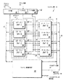
図3は、図2のタグアレイ43の一部の一実施形態を示す。例示した実施形態において、アドレス0用のビット0及びビット1を示す。他の実施形態は、各アドレスに対応する任意の所望数のビットを有し得る(例えば、アドレス0が、8ビット、9ビット、16ビット、32ビット、64ビットに対応し得る等)。例示した実施形態の場合、所定のアドレス(例えば、アドレス0)の各ビット(例えば、ビット0)は、各経路(例えば、経路0、経路1、経路2、経路3)用の別個の部分を有することに留意されたい。また、タグアレイ43は、任意の所望数のアドレス(例えば、Nを整数とすると、アドレス0乃至アドレスN)を有し得ることに留意されたい。例示した実施形態において、アドレス0用のビット0には、経路0用の回路、経路1用の回路、経路2用の回路、及び経路3用の回路を含む回路100が含まれる。
FIG. 3 illustrates one embodiment of a portion of the
図3は、ビットセルを含むタグアレイ43の部分だけを示すことを当業者は認識されるであろう。各ビットセルには、記憶要素(1つ又は複数)と、記憶要素(1つ又は複数)の読出し及び書き込みを行うためのトランジスタと、が含まれる(図4参照)。図3に示さないタグアレイ43の部分は、任意の適切な従来技術による方法を含む任意の所望の方法で実現し得る。例えば、幾つかの実施形態において、タグアレイ43には、アドレス、制御、及び書き込みデータ用の入力ラッチが含まれることがある。更に、アドレスデコーダ、ワード線ドライバ、及び列回路が存在することがある。列回路は、列多重化装置、センス増幅器又はデータインバータ、出力ドライバ、及び出力ラッチを包含し得るが、これらは、全て任意の適切な従来技術による方法を含む任意の所望の方法で実現し得る。本明細書に用いる用語「ビットセル」は、記憶回路の1つのタイプである。
Those skilled in the art will recognize that FIG. 3 shows only the portion of the
更に、1つのタグ経路だけが、所定の時間に書き込まれることがあることを当業者は認識されるであろう。更に一般的には、所定の入力項目用のビットセルの一部(ワード線)だけを書き込む必要があることは、極めて普通のことである。従って、ビットセルの残りは、それらの元の状態を保持すべきである。一般的に用いられる従来技術は、ワード線に関連する全てのビットセル用のプリチャージされた書き込みビット線対(ビット線及びビット線バー)を用いることによって、この機能を達成する。更新する必要がないビットセルは、第2電源電圧(例えば、電力又はVDD)に実質的に近い値でプリチャージされたままであるビット線及びビット線バーを有する。更新する必要があるビットセルは、ビット線及びビット線バー用の(VDDに近いものに対して接地に近いもの又はその逆の)相補値を有する。 Furthermore, those skilled in the art will recognize that only one tag path may be written at a given time. More generally, it is quite common to write only a portion of a bit cell (word line) for a given input item. Therefore, the rest of the bit cells should retain their original state. The commonly used prior art accomplishes this function by using a precharged write bit line pair (bit line and bit line bar) for all bit cells associated with the word line. Bit cells that do not need to be updated have bit lines and bit line bars that remain precharged at a value substantially close to a second power supply voltage (eg, power or VDD). Bit cells that need to be updated have complementary values for bit lines and bit line bars (close to VDD vs. close to ground or vice versa).
上記パラグラフに述べた解決策は、当業者によって通常用いられる。しかしながら、それは、低消費電力及び低電圧動作を必要とする用途に対して固有の弱さを有する。特に、更新する必要がないビットセルは、依然としてそれらの選択トランジスタ(1つ又は複数)が導通状態にあることに留意すべきである。その結果、ビットセルの内部記憶ノードは、VDD近くにプリチャージされたビット線及びビット線バー信号にさらされる。その結果、ビットセルの“論理0”側に関連するビット線(又はビット線バー)から流れる電流が存在する。これは、ビット線(又はビット線バー)を部分的に放電する“ダミー読出し”動作である。結局、部分的に放電されるビット線(又はビット線バー)は、プリチャージ動作中、再び補充する必要がある。従って、これは、無駄な電力である。
The solutions described in the above paragraph are commonly used by those skilled in the art. However, it has inherent weaknesses for applications that require low power consumption and low voltage operation. In particular, it should be noted that bit cells that do not need to be updated still have their select transistor (s) in a conducting state. As a result, the internal storage node of the bit cell is exposed to the bit line and bit line bar signal precharged near VDD. As a result, there is current flowing from the bit line (or bit line bar) associated with the “
無駄な電力とは別に、この解決策固有の他の弱さがある。特に、“ダミー読出し”では、ビットセルの内部記憶ノードが、プリチャージされたビット線及びビット線バーにさらされる必要がある。すると、このことにより、ビットセルの状態が意図せずに変わる可能性がある。これを保護するために、ビットセルトランジスタは、ダミー読出し中、安定性が改善されるように大きさが決定されなければならない。このことの副作用は、これによって、ビットセルが低電圧で書き込むのが更に困難になることである。 Apart from wasted power, there are other weaknesses inherent in this solution. In particular, in the “dummy read”, the internal storage node of the bit cell needs to be exposed to the precharged bit line and the bit line bar. As a result, the state of the bit cell may change unintentionally. To protect this, the bit cell transistor must be sized to improve stability during the dummy read. A side effect of this is that it makes it more difficult for the bit cell to write at a low voltage.
図4に示す提案された解決策は、書き込まれる予定の各タグ経路に個別書き込みワード線を用いることによって、“ダミー読出し”を無くする。個別書き込みワード線によって、ビットセル面積が必ずしも増えるとは限らない。その理由は、これが、一般的に、メタルレイアウトルールに対して、トランジスタレイアウトルールによって支配されるためである。更に、図4の提案された解決策は、4つの経路用の全ての書き込み金属ビット線を1つの共用金属ビット線(及び/又はビット線バー)に統合する。この利点について、図4に関連する説明で議論する。 The proposed solution shown in FIG. 4 eliminates “dummy read” by using a separate write word line for each tag path to be written. The individual write word lines do not necessarily increase the bit cell area. The reason is that this is generally governed by transistor layout rules over metal layout rules. Further, the proposed solution of FIG. 4 combines all the write metal bit lines for the four paths into one shared metal bit line (and / or bit line bar). This advantage will be discussed in the description associated with FIG.
図4は、図3の回路100(経路0−3用のアドレス0のビット0)の一実施形態を示す。経路0用の記憶セル112には、交差接続インバータ116及び117が含まれる。記憶セル112は、トランジスタ124の第1電流電極に接続された第1端子及びトランジスタ125の第1電流電極に接続された第2端子を有する。トランジスタ124及び125の制御電極は、双方共、書き込みワード線(経路0)108に接続される。記憶セル112の第2端子は、トランジスタ136の制御電極に接続される。トランジスタ136の第1電流電極は、第1電源電圧に接続される。トランジスタ136の第2電流電極は、トランジスタ132の第1電流電極に接続される。読出しワード線107は、トランジスタ132の制御電極に接続される。トランジスタ132の第2電流電極は、読出しビット線(経路0)103に接続される。
FIG. 4 illustrates one embodiment of the
経路1用の記憶セル113には、交差接続インバータ118及び119が含まれる。記憶セル113は、トランジスタ126の第1電流電極に接続された第1端子及びトランジスタ127の第1電流電極に接続された第2端子を有する。トランジスタ126及び127の制御電極は、双方共、書き込みワード線(経路1)109に接続される。トランジスタ126の第2電流電極は、トランジスタ124の第2電流電極及び書き込みビット線バー102に接続される。用語「バー」は、相補信号を示すために用いられる(例えば、書き込みビット線バー102は、書き込みビット線101に対して補完的である)ことに留意されたい。トランジスタ127の第2電流電極は、トランジスタ125の第2電流電極及び書き込みビット線101に接続される。記憶セル113の第2端子は、トランジスタ137の制御電極に接続される。トランジスタ137の第1電流電極は、第1電源電圧に接続される。トランジスタ137の第2電流電極は、トランジスタ133の第1電流電極に接続される。読出しワード線107は、トランジスタ133の制御電極に接続される。トランジスタ133の第2電流電極は、読出しビット線(経路1)104に接続される。回路180は、経路0に用いられ、回路181は、経路1に用いられる。
The
経路2用の記憶セル114には、交差接続インバータ120及び121が含まれる。記憶セル114は、トランジスタ128の第1電流電極に接続された第1端子及びトランジスタ129の第1電流電極に接続された第2端子を有する。トランジスタ128及び129の制御電極は、双方共、書き込みワード線(経路2)110に接続される。記憶セル114の第2端子は、トランジスタ138の制御電極に接続される。トランジスタ138の第1電流電極は、第1電源電圧に接続される。トランジスタ138の第2電流電極は、トランジスタ134の第1電流電極に接続される。読出しワード線107は、トランジスタ134の制御電極に接続される。トランジスタ134の第2電流電極は、読出しビット線(経路2)105に接続される。
The memory cell 114 for
経路3用の記憶セル115には、交差接続インバータ122及び123が含まれる。記憶セル115は、トランジスタ130の第1電流電極に接続された第1端子及びトランジスタ131の第1電流電極に接続された第2端子を有する。トランジスタ130及び131の制御電極は、双方共、書き込みワード線(経路3)111に接続される。トランジスタ130の第2電流電極は、トランジスタ128の第2電流電極及び書き込みビット線バー102に接続される。トランジスタ131の第2電流電極は、トランジスタ129の第2電流電極及び書き込みビット線101に接続される。記憶セル115の第2端子は、トランジスタ139の制御電極に接続される。トランジスタ139の第1電流電極は、第1電源電圧に接続される。トランジスタ139の第2電流電極は、トランジスタ135の第1電流電極に接続される。読出しワード線107は、トランジスタ135の制御電極に接続される。トランジスタ135の第2電流電極は、読出しビット線(経路3)106に接続される。回路182は、経路2に用いられ、回路183は、経路3に用いられる。図4に示すトランジスタは、全てnチャネル電界効果トランジスタである。他の実施形態は、代わりに、pチャネル電界効果トランジスタ、又は回路100内で適切に接続されたnチャネル及びpチャネルトランジスタの組合せを用い得る。
The memory cell 115 for
図4の回路100の幾つかの実施形態の場合、第1電源電圧は、ほぼ接地電圧であってよく、第2電源電圧は、第1電源電圧より高くてよく、また、プリチャージする(例えば、図4の読出しビット線103−106をプリチャージする)目的に用いてよい。
For some embodiments of the
図4の回路100は、アドレス(例えば、アドレス0)における追加の各ビットに対して複製されることに留意されたい。更に、回路100は、アドレス0からアドレスNまでのアドレスにおける各ビット0に対しても複製される。例えば、アドレス1のビット0は、回路100の複製を利用する。
Note that the
図4の回路100に示した特定の実施形態には、上述したもの以外の多くの恩恵がある。書き込みビット線(101及び102)を共用することによって、また、各記憶回路(180−183)用にそれらを複製しないことによって、ルーティングが低減されることを当業者は認識されるであろう。これによって、読出しビット線(103−106)の間隔が大きくなって寄生容量が減少し、また、読出しビット線(103−106)の幅が広くなって導体配線の寄生抵抗が減少し得る。これら恩恵のいずれかによって、回路100の読出し動作を高速化し得る。更に、回路100に示した実施形態は、記憶要素を用いる他の用途より書き込みビット線(101及び102)が少なく、従って、書き込みビット線(101及び102)を駆動するのに必要な回路が低減される。これは、用いる回路が小さくなり、また、寄生電力消費を受けるデバイスが少なくなり得ることを意味する。従って、必要な半導体面積が小さくなり、漏れ電流が小さくなり得る。
The particular embodiment shown in
次に、図4の回路100の読出し動作の一実施形態について述べる。一実施形態において、アドレス0に対する読出し動作中、読出しワード線107がアサートされ、これにより、トランジスタ132、133、134、及び135が導通状態になる。トランジスタ136、137、138、及び139は、それぞれ記憶セル112、113、114、及び115に記憶された値に基づき、導通状態又は非導通状態のいずれかである。トランジスタ136が導通状態である場合、プリチャージされた読出しビット線(経路0)103は、論理レベル“1”から論理レベル“0”に放電される。トランジスタ137が非導通状態である場合、プリチャージされた読出しビット線(経路1)104は、論理レベル“0”に放電されない。読出しビット線(経路2)105及び読出しビット線(経路3)106は、トランジスタ138及び139が導通状態又は非導通状態かどうかに依存して、放電されたり放電されなかったりする。例示した実施形態では、全経路(経路0−3)が同時に読み出されることに留意されたい。
Next, an embodiment of the read operation of the
次に、図4の回路100の書き込み動作の一実施形態について述べる。一実施形態では、書き込み動作中、一度に1つの経路だけが書き込まれる。例えば、経路0のアドレス0への書き込みアクセスの場合、書き込みワード線(経路0)108が、アサートされ、他の全ての書き込みワード線109−111は、アサートされない。書き込まれるデータは、書き込みビット線101に印加又は供給され、補完データは、書き込みビット線バー102に印加又は供給される。書き込みワード線(経路0)108がアサートされると、トランジスタ124及び125は、導通状態になる。これによって、記憶セル112の2つの端子は、書き込みデータ値を記憶セル112に伝達するために、それぞれ書き込みビット線101及び書き込みビット線バー102に接続される。
Next, an embodiment of the write operation of the
例示した実施形態の場合、読出しアクセス及び書き込みアクセスは、互いに独立であることに留意されたい。従って、読出し動作及び書き込み動作は、読出しアクセスが、書き込みアクセスと異なるアドレスに対するものであれば、同時に起こり得る。従って、例示した実施形態の場合、異なるアドレスへの読出しアクセス及び書き込みアクセスは、時間的に、同時に、部分的に重なり合って、又は重なり合わずに起こり得る。 Note that for the illustrated embodiment, read access and write access are independent of each other. Therefore, the read operation and the write operation can occur simultaneously if the read access is for an address different from the write access. Thus, for the illustrated embodiment, read and write accesses to different addresses can occur in time, simultaneously, partially overlapping, or non-overlapping.
本発明の他の実施形態は、わずかな回路を追加することによって、追加の読出し及び/又は書き込みポートを追加し得ることに留意されたい。例えば、追加の読出しポートは、各経路用にトランジスタ132及び136、133及び137、134及び138、並びに135及び139と並列に別のトランジスタを追加することによって、また、別の読出しワード線及び別の読出しビット線を追加することによって、追加し得る。追加の書き込みポートは、各経路用にトランジスタ124及び125、126及び127、128及び129、並びに130及び131と並列に別のトランジスタを追加することによって、また、別の書き込みワード線及び別の書き込みビット線を追加することによって、追加し得る。
Note that other embodiments of the present invention may add additional read and / or write ports by adding a few circuits. For example, additional read ports can be added by adding another transistor in parallel with
次に、図5において、図5の回路200は、キャッシュ18の文脈でも用い得るが、レジスタファイル(例えば、図1のレジスタファイル17)の文脈で述べる。従って、キャッシュに用いられる“経路”の概念の代わりに、“文脈”の概念を用いる。例えば、レジスタファイル17は、文脈スイッチングに、例えば、多数のタスク又はスレッドが用いられる場合に用い得る。本発明は、任意の所望の用途に用い得ること、及び本明細書において述べた用途(例えば、キャッシュ経路、文脈スイッチング)は、単に2つの可能な用途であることに留意されたい。更に、図4及び5で本明細書に述べた回路は、データ処理システム10の任意の部分に、例えば、レジスタファイル17、(例えば、潜在的な枝路アドレスを記憶するための)分岐ユニット15、SRAM19、他のモジュール20、キャッシュ18、バッファ21、及びメモリ14等に用い得る。他の実施形態は、任意の所望の方法で、また、任意の所望の用途に、図4−5に示す回路を用い得る。
Next, in FIG. 5,
図5は、図1のレジスタファイル17の一部の回路200の一実施形態(文脈0−1用のアドレス0のビット0)を示す。文脈0用の記憶セル212には、交差接続インバータ216及び217が含まれる。記憶セル212は、トランジスタ224の第1電流電極に接続された第1端子及びトランジスタ225の第1電流電極に接続された第2端子を有する。トランジスタ224及び225の制御電極は、双方共、書き込みワード線(文脈0)208に接続される。記憶セル212の第2端子は、トランジスタ236の制御電極に接続される。トランジスタ236の第1電流電極は、第1電源電圧に接続される。トランジスタ236の第2電流電極は、トランジスタ232の第1電流電極に接続される。読出しワード線206は、トランジスタ232の制御電極に接続される。トランジスタ232の第2電流電極は、読出しビット線203に接続される。
FIG. 5 shows one embodiment of a
文脈1用の記憶セル213には、交差接続インバータ218及び219が含まれる。記憶セル213は、トランジスタ226の第1電流電極に接続された第1端子及びトランジスタ227の第1電流電極に接続された第2端子を有する。トランジスタ226及び227の制御電極は、双方共、書き込みワード線(文脈1)209に接続される。トランジスタ226の第2電流電極は、トランジスタ224の第2電流電極及び書き込みビット線バー202に接続される。トランジスタ227の第2電流電極は、トランジスタ225の第2電流電極及び書き込みビット線201に接続される。記憶セル213の第2端子は、トランジスタ237の制御電極に接続される。トランジスタ237の第1電流電極は、第1電源電圧に接続される。トランジスタ237の第2電流電極は、トランジスタ233の第1電流電極に接続される。読出しワード線207は、トランジスタ233の制御電極に接続される。トランジスタ233の第2電流電極は、読出しビット線203に接続される。回路280は、文脈0に用いられ、回路281は、文脈1に用いられる。図5に示すトランジスタは、全てnチャネル電界効果トランジスタである。他の実施形態は、代わりに、pチャネル電界効果トランジスタ、又は回路200内で適切に接続されたnチャネル及びpチャネルトランジスタの組合せを用い得る。
図5の回路200の幾つかの実施形態の場合、第1電源電圧は、ほぼ接地電圧であってよく、第2電源電圧は、第1電源電圧より高くてよく、また、プリチャージする(例えば、図5の読出しビット線203をプリチャージする)目的に用いてよい。
For some embodiments of the
図5の回路200は、アドレス(例えば、アドレス0)における追加の各ビットに対して複製されることに留意されたい。更に、回路200は、アドレス0からアドレスNまでのアドレスにおける各ビット0に対しても複製される。例えば、アドレス1のビット0は、回路200の複製を利用する。
Note that the
図5に示す回路は、単一の読出しポート及び単一の書き込みポートによる2スレッドレジスタファイル(例えば、図1のレジスタファイル17)での用途に適用可能である。各スレッド(即ち、“文脈”)は、別個の記憶要素212、213によって表される。所定の時間において、レジスタファイル17のアクセスが、2つのスレッドの内の1つにおいて起こる。例えば、この特定のビットへの書き込み動作は、適切な書き込みワード線(208又は209)上において、論理レベル“1”を必然的に伴う。アクセスされないスレッドは、その書き込みワード線が、論理レベル“0”である。そして、書き込みビット線201及び202上に存在するデータ値は、それぞれの選択トランジスタ(224及び225、226及び227)を通して、適切な記憶セル212及び213に接続される。
The circuit shown in FIG. 5 is applicable for use with a two thread register file (eg, register
次に、図5の回路200用の読出し動作の一実施形態について述べる。例示した実施形態において、読出しアクセスでは、適切な読出しワード線(206又は207)が論理レベル“1”である必要がある。一実施形態において、文脈0に対する読出し動作中、読出しワード線206が、アサートされ(即ち、論理レベル“1”)、これによって、トランジスタ232が導通状態になり、トランジスタ233は、実質的に非導通状態になる。その結果、記憶セル212に記憶された値は、この時点で、読出しビット線203の合成値を決定する。一実施形態において、読出しビット線203は、初期的に論理レベル“1”にプリチャージした。読出しビット線203は、論理レベル“0”に放電するか、又は、論理レベル“1”にプリチャージされたままである。一実施形態において、読出しビット線203の値は、インバータ又はバッファ(図示せず)のいずれかを通して、レジスタファイル17データ出力バス(図示せず)に接続してよい。上記読出し動作の場合、トランジスタ233が実質的に非導通状態であるという事実により、記憶セル213に記憶された値は、読出しビット線203に影響を及ぼさないことに留意されたい。
Next, an embodiment of a read operation for the
図5の上記説明は、具体的には、単一の読出しポート及び単一の書き込みポートの場合に該当する。しかしながら、図5に示す回路は、簡単に多数の読出しポート及び/又は多数の書き込みポートの場合に拡張し得る。図5の例示した実施形態において、読出しポートを追加すると、(積層236、232及び積層233、237と同様な)nチャネル直列積層に各々接続される読出しワード線(206、207等)の追加及び読出しビット線(203等)の追加が必然的に伴う。書き込みポートを追加すると、選択トランジスタ(224、225及び226、227等)に各々接続される書き込みワード線(208、209等)及び書き込みビット線(201、202等)の追加が必然的に伴う。
The above description of FIG. 5 specifically corresponds to the case of a single read port and a single write port. However, the circuit shown in FIG. 5 can be easily extended to multiple read ports and / or multiple write ports. In the illustrated embodiment of FIG. 5, the addition of a read port adds the addition of read word lines (206, 207, etc.) each connected to an n-channel serial stack (similar to
上記明細書において、具体的な実施形態を参照して、本発明について説明した。しかしながら、当業者が理解されるように、以下の請求項に記載した本発明の範囲から逸脱することなく、様々な修正及び変更を行い得る。例えば、読出し及び/又は書き込みビット線は、単一端ビット線であってよく又は他の選択肢としてビット線対であってよい。ビット線対の場合、多くの可能性がある。例えば、ビット線対は、予めハイに充電したり、予めローに充電したり、接地とVDDとの間の値にプリチャージしたり、小信号差動電圧を担持したり、あるいは、全レール相補電圧を担持し得る。したがって、明細書及び図は、限定的でなく例示的であると見なすものとし、また、そのような全ての修正は、本発明の範囲内に含まれるものとする。 In the foregoing specification, the invention has been described with reference to specific embodiments. However, one of ordinary skill in the art appreciates that various modifications and changes can be made without departing from the scope of the present invention as set forth in the claims below. For example, the read and / or write bit lines may be single-ended bit lines or alternatively bit line pairs. In the case of bit line pairs, there are many possibilities. For example, bit line pairs can be precharged high, precharged low, precharged to a value between ground and VDD, carry a small signal differential voltage, or all rail complementary It can carry a voltage. The specification and drawings are accordingly to be regarded as illustrative rather than restrictive, and all such modifications are intended to be included within the scope of the present invention.
恩恵、他の利点、及び問題の解決策について、具体的な実施形態を基にこれまで述べた。しかしながら、これらの恩恵、利点、問題の解決策、及び何らかの恩恵、利点、又は解決策を生じさせる又はより顕著にさせる如何なる要素(1つ又は複数)も、全ての請求項の重要な、必要な、若しくは不可欠な特徴又は要素として解釈してはならない。本明細書に用いた用語「“a”又は“an”(不定冠詞)」は、1つ又は1つ以上と定義する。本明細書に用いた用語「“including”(含む)」及び/又は「“having”(有する)」は、「“comprising”(含む)」(即ち、オープンランゲージ)と定義する。本明細書に用いた用語「“comprises”(含む)」、「“comprising”(含む)」又はその派生語は、非排他的な包括を網羅するものであり、一連の要素を含むプロセス、方法、物、又は装置が、これらの要素だけでなく、明示的に列記されていない他の要素や、このようなプロセス、方法、物、又は装置に固有の他の要素も含み得る。 Benefits, other advantages, and solutions to problems have been described above based on specific embodiments. However, these benefits, advantages, solutions to problems, and any element (s) that cause or make any benefit, advantage, or solution important or necessary in all claims Or as an essential feature or element. The term “a” or “an” (indefinite article) as used herein is defined as one or more than one. The terms “including” and / or “having” as used herein are defined as “comprising” (ie, open language). As used herein, the terms “comprises”, “comprising” or derivatives thereof are intended to cover non-exclusive inclusions and include a series of elements. , Objects, or devices may include not only these elements, but also other elements not explicitly listed, as well as other elements unique to such processes, methods, objects, or devices.
Claims (21)
第1端子及び第2端子を有し第2データ値を記憶するための第2記憶セルと、
前記第1記憶セル及び前記第2記憶セルの各々に接続され、それぞれ前記第1データ値及び前記第2データ値双方を前記第1記憶セル及び前記第2記憶セルに選択的に提供するための共用書き込みビット線と、
前記第1記憶セルに接続され、前記第1記憶セルだけを選択的に読み出すための第1読出しビット線と、
前記第2記憶セルに接続され、前記第2記憶セルだけを選択的に読み出すための第2読出しビット線と、
が含まれる記憶回路。 A first memory cell having a first terminal and a second terminal for storing a first data value;
A second memory cell having a first terminal and a second terminal for storing a second data value;
Connected to each of the first memory cell and the second memory cell for selectively providing both the first data value and the second data value to the first memory cell and the second memory cell, respectively. A shared write bit line;
A first read bit line connected to the first memory cell for selectively reading only the first memory cell;
A second read bit line connected to the second memory cell for selectively reading only the second memory cell;
Including a memory circuit.
前記第2記憶セルの前記第2端子に接続された第2選択ゲートと、
前記第1選択ゲートに接続された、同第1選択ゲートによる前記第1記憶セルへの書き込みを可能にする第1書き込みワード線と、
前記第2選択ゲートに接続された、前記第2選択ゲートによる前記第2記憶セルへの書き込みを可能にする前記第2書き込みワード線と、
が含まれる請求項1に記載の記憶回路。 A first select gate connected to the first terminal of the first memory cell;
A second select gate connected to the second terminal of the second memory cell;
A first write word line connected to the first select gate and enabling writing to the first memory cell by the first select gate;
The second write word line connected to the second select gate and enabling writing to the second memory cell by the second select gate;
The memory circuit according to claim 1, wherein:
前記第2記憶セルの前記第1端子に接続された、前記第2書き込みワード線によって制御される第4選択ゲートと、
が含まれる請求項4に記載の記憶回路。 A third select gate connected to the second terminal of the first memory cell and controlled by the first write word line;
A fourth select gate connected to the first terminal of the second memory cell and controlled by the second write word line;
The memory circuit according to claim 4, wherein:
第1端子及び第2端子を有する第1記憶セルに第1データ値を記憶する段階と、
第1端子及び第2端子を有する第2記憶セルに第2データ値を記憶する段階と、
それぞれ前記第1データ値及び前記第2データ値双方を前記第1記憶セル及び前記第2記憶セルに選択的に提供するための共用書き込みビット線を前記第1記憶セル及び前記第2記憶セルの各々に接続する段階と、
前記第1記憶セルに接続された第1読出しビット線を介して前記第1記憶セルだけを選択的に読み出す段階と、
前記第2記憶セルに接続された第2読出しビット線を介して前記第2記憶セルだけを選択的に読み出す段階と、
が含まれる方法。 A method for processing data in a data storage circuit, comprising:
Storing a first data value in a first memory cell having a first terminal and a second terminal;
Storing a second data value in a second memory cell having a first terminal and a second terminal;
A shared write bit line for selectively providing both the first data value and the second data value to the first memory cell and the second memory cell, respectively, of the first memory cell and the second memory cell. Connecting to each;
Selectively reading only the first memory cell through a first read bit line connected to the first memory cell;
Selectively reading only the second memory cell via a second read bit line connected to the second memory cell;
Include methods.
前記第1記憶セルを書き込む段階と、
第2書き込みワード線を介して前記第2記憶セルの前記第2端子に接続された第2選択ゲートをイネーブル状態にする段階と、
前記第2記憶セルを書き込む段階と、
が含まれる請求項7に記載の方法。 And enabling a first select gate connected to the first terminal of the first memory cell via a first write word line;
Writing the first memory cell;
Enabling a second select gate connected to the second terminal of the second memory cell via a second write word line;
Writing the second memory cell;
8. The method of claim 7, wherein
前記第2記憶セルの前記第1端子に接続された第4選択ゲートを提供する段階であって、前記第4選択ゲートは、前記第2書き込みワード線によって制御される前記段階と、
が含まれる請求項10に記載の方法。 And providing a third select gate connected to the second terminal of the first memory cell, the third select gate being controlled by the first write word line;
Providing a fourth select gate connected to the first terminal of the second memory cell, wherein the fourth select gate is controlled by the second write word line;
11. The method of claim 10, wherein
前記連想メモリの第2経路に前記第2記憶セルを割り当てる段階と、
が含まれる請求項10に記載の方法。 And assigning the first memory cell to the first path of the content addressable memory;
Allocating the second memory cell to the second path of the content addressable memory;
11. The method of claim 10, wherein
第1端子及び第2端子を有し第1データ値を記憶するための第1記憶セルと、
第1端子及び第2端子を有し第2データ値を記憶するための第2記憶セルと、
前記第1記憶セルに接続され、前記第1記憶セルだけに選択的に書き込むための第1書き込みワード線と、
前記第2記憶セルに接続され、前記第2記憶セルだけに選択的に書き込むための第2書き込みワード線と、
前記第1記憶セルに接続された第1選択ゲート及び前記第2記憶セルに接続された第2選択ゲートと、
前記第1選択ゲート及び前記第2選択ゲートの各々に接続され、それぞれ前記第1データ値及び前記第2データ値双方を前記第1記憶セル及び前記第2記憶セルから提供する制御信号を選択的に提供するための共用読出しワード線と、
が含まれる記憶回路。 A memory circuit,
A first memory cell having a first terminal and a second terminal for storing a first data value;
A second memory cell having a first terminal and a second terminal for storing a second data value;
A first write word line connected to the first memory cell for selectively writing only to the first memory cell;
A second write word line connected to the second memory cell for selectively writing only to the second memory cell;
A first select gate connected to the first memory cell and a second select gate connected to the second memory cell;
A control signal connected to each of the first selection gate and the second selection gate and selectively providing both the first data value and the second data value from the first memory cell and the second memory cell, respectively. A shared read word line to provide
Including a memory circuit.
第1端子及び第2端子を有し第1データ値を記憶するための第1記憶セルと、
第1端子及び第2端子を有し第2データ値を記憶するための第2記憶セルと、
前記第1記憶セル及び前記第2記憶セルの各々に接続され、それぞれ前記第1データ値及び前記第2データ値双方を前記第1記憶セル及び前記第2記憶セルに選択的に提供するための共用書き込みビット線と、
前記第1記憶セルの読出しを選択的に可能にするための第1読出し選択ゲート及び前記第2記憶セルの読出しを選択的に可能にするための第2読出し選択ゲートと、
前記第1読出し選択ゲート及び前記第2読出し選択ゲートの各々に接続され、前記第1記憶セル及び前記第2記憶セルの各々を選択的に読み出すための共用読出しビット線と、
が含まれる記憶回路。 A memory circuit,
A first memory cell having a first terminal and a second terminal for storing a first data value;
A second memory cell having a first terminal and a second terminal for storing a second data value;
Connected to each of the first memory cell and the second memory cell for selectively providing both the first data value and the second data value to the first memory cell and the second memory cell, respectively. A shared write bit line;
A first read selection gate for selectively enabling reading of the first storage cell and a second read selection gate for selectively enabling reading of the second storage cell;
A shared read bit line connected to each of the first read select gate and the second read select gate for selectively reading each of the first memory cell and the second memory cell;
Including a memory circuit.
前記第1記憶セル及び前記第2記憶セルを選択的に別々に読み出すための前記第1記憶セルに接続された第1読出しワード線及び前記第2記憶セルに接続された第2読出しワード線と、
が含まれる請求項15に記載の記憶回路。 Further, a first write word line connected to the first memory cell and a second write word connected to the second memory cell for selectively writing the first memory cell and the second memory cell separately. Lines and,
A first read word line connected to the first memory cell and a second read word line connected to the second memory cell for selectively reading the first memory cell and the second memory cell separately; ,
The memory circuit according to claim 15.
第1端子及び第2端子を有し第1データ値を記憶するための第1記憶セルを提供する段階と、
第1端子及び第2端子を有し第2データ値を記憶するための第2記憶セルを提供する段階と、
それぞれ前記第1データ値及び前記第2データ値双方を前記第1記憶セル及び前記第2記憶セルに選択的に提供するための共用書き込みビット線を前記第1記憶セル及び前記第2記憶セル各々の前記第1端子に接続する段階と、
前記第1記憶セル及び前記第2記憶セル各々を選択的に読み出すための共用読出しビット線を前記第1記憶セル及び前記第2記憶セル各々に接続する段階と、が含まれる方法。 A method for processing data in a data storage circuit, comprising:
Providing a first storage cell having a first terminal and a second terminal for storing a first data value;
Providing a second memory cell having a first terminal and a second terminal for storing a second data value;
Each of the first memory cell and the second memory cell has a shared write bit line for selectively providing both the first data value and the second data value to the first memory cell and the second memory cell, respectively. Connecting to the first terminal of
Connecting a shared read bit line for selectively reading each of the first memory cell and the second memory cell to each of the first memory cell and the second memory cell.
前記第1記憶セル及び前記第2記憶セルを選択的に別々に読み出すために、第1読出しワード線を前記第1記憶セルに接続し、第2読出しワード線を前記第2記憶セルに接続する段階と、が含まれる請求項18に記載の方法。 Further, in order to selectively write the first memory cell and the second memory cell separately, a first write word line is connected to the first memory cell, and a second write word line is connected to the second memory cell. Connecting, and
In order to selectively read the first memory cell and the second memory cell separately, a first read word line is connected to the first memory cell, and a second read word line is connected to the second memory cell. The method of claim 18, comprising:
データ処理システムにおいて、第1文脈又は第1スレッドに前記第1記憶セルを割り当てる段階と、
前記データ処理システムにおいて、第2文脈又は第2スレッドに前記第2記憶セルを割り当てる段階と、が含まれる方法。 The method of claim 18, further comprising:
Allocating the first storage cell to a first context or a first thread in a data processing system;
Assigning the second storage cell to a second context or a second thread in the data processing system.
Applications Claiming Priority (2)
| Application Number | Priority Date | Filing Date | Title |
|---|---|---|---|
| US11/132,457 US7295487B2 (en) | 2005-05-19 | 2005-05-19 | Storage circuit and method therefor |
| PCT/US2006/011560 WO2006127117A2 (en) | 2005-05-19 | 2006-03-29 | Storage circuit and method therefor |
Publications (2)
| Publication Number | Publication Date |
|---|---|
| JP2008541333A true JP2008541333A (en) | 2008-11-20 |
| JP2008541333A5 JP2008541333A5 (en) | 2009-05-14 |
Family
ID=37448177
Family Applications (1)
| Application Number | Title | Priority Date | Filing Date |
|---|---|---|---|
| JP2008512275A Pending JP2008541333A (en) | 2005-05-19 | 2006-03-29 | Memory circuit and method thereof |
Country Status (5)
| Country | Link |
|---|---|
| US (2) | US7295487B2 (en) |
| JP (1) | JP2008541333A (en) |
| KR (1) | KR20080009129A (en) |
| TW (1) | TWI336476B (en) |
| WO (1) | WO2006127117A2 (en) |
Cited By (1)
| Publication number | Priority date | Publication date | Assignee | Title |
|---|---|---|---|---|
| US8908406B2 (en) | 2011-06-09 | 2014-12-09 | Semiconductor Energy Laboratory Co., Ltd. | Cache memory and method for driving the same |
Families Citing this family (6)
| Publication number | Priority date | Publication date | Assignee | Title |
|---|---|---|---|---|
| TWI455148B (en) * | 2010-12-13 | 2014-10-01 | Vanguard Int Semiconduct Corp | Integrated device for accessing multi-port input read/write event |
| JP6012263B2 (en) | 2011-06-09 | 2016-10-25 | 株式会社半導体エネルギー研究所 | Semiconductor memory device |
| US9208859B1 (en) | 2014-08-22 | 2015-12-08 | Globalfoundries Inc. | Low power static random access memory (SRAM) read data path |
| US9786359B2 (en) | 2016-01-29 | 2017-10-10 | Taiwan Semiconductor Manufacturing Company, Ltd. | Static random access memory (SRAM) tracking cells and methods of forming same |
| US9940996B1 (en) | 2017-03-01 | 2018-04-10 | Nxp Usa, Inc. | Memory circuit having increased write margin and method therefor |
| US9934846B1 (en) | 2017-03-01 | 2018-04-03 | Nxp Usa, Inc. | Memory circuit and method for increased write margin |
Citations (5)
| Publication number | Priority date | Publication date | Assignee | Title |
|---|---|---|---|---|
| JPH06215580A (en) * | 1993-01-18 | 1994-08-05 | Mitsubishi Electric Corp | Memory cell circuit |
| JPH08161890A (en) * | 1994-12-02 | 1996-06-21 | Fujitsu Ltd | Memory cell circuit and multi-port semiconductor storage |
| JPH09120679A (en) * | 1995-07-27 | 1997-05-06 | Texas Instr Inc <Ti> | High-density memory cell of two-port type |
| JP2005044456A (en) * | 2003-07-24 | 2005-02-17 | Renesas Technology Corp | Semiconductor memory device |
| JP2005050479A (en) * | 2003-07-31 | 2005-02-24 | Nec Micro Systems Ltd | Semiconductor memory and its reference potential generation method |
Family Cites Families (3)
| Publication number | Priority date | Publication date | Assignee | Title |
|---|---|---|---|---|
| US5854761A (en) * | 1997-06-26 | 1998-12-29 | Sun Microsystems, Inc. | Cache memory array which stores two-way set associative data |
| US6282143B1 (en) * | 1998-05-26 | 2001-08-28 | Hewlett-Packard Company | Multi-port static random access memory design for column interleaved arrays |
| US6804143B1 (en) * | 2003-04-02 | 2004-10-12 | Cogent Chipware Inc. | Write-assisted SRAM bit cell |
-
2005
- 2005-05-19 US US11/132,457 patent/US7295487B2/en active Active
-
2006
- 2006-03-29 KR KR1020077026821A patent/KR20080009129A/en not_active Application Discontinuation
- 2006-03-29 JP JP2008512275A patent/JP2008541333A/en active Pending
- 2006-03-29 WO PCT/US2006/011560 patent/WO2006127117A2/en active Application Filing
- 2006-04-10 TW TW095112657A patent/TWI336476B/en active
-
2007
- 2007-10-01 US US11/865,495 patent/US7525867B2/en active Active
Patent Citations (5)
| Publication number | Priority date | Publication date | Assignee | Title |
|---|---|---|---|---|
| JPH06215580A (en) * | 1993-01-18 | 1994-08-05 | Mitsubishi Electric Corp | Memory cell circuit |
| JPH08161890A (en) * | 1994-12-02 | 1996-06-21 | Fujitsu Ltd | Memory cell circuit and multi-port semiconductor storage |
| JPH09120679A (en) * | 1995-07-27 | 1997-05-06 | Texas Instr Inc <Ti> | High-density memory cell of two-port type |
| JP2005044456A (en) * | 2003-07-24 | 2005-02-17 | Renesas Technology Corp | Semiconductor memory device |
| JP2005050479A (en) * | 2003-07-31 | 2005-02-24 | Nec Micro Systems Ltd | Semiconductor memory and its reference potential generation method |
Cited By (1)
| Publication number | Priority date | Publication date | Assignee | Title |
|---|---|---|---|---|
| US8908406B2 (en) | 2011-06-09 | 2014-12-09 | Semiconductor Energy Laboratory Co., Ltd. | Cache memory and method for driving the same |
Also Published As
| Publication number | Publication date |
|---|---|
| KR20080009129A (en) | 2008-01-24 |
| WO2006127117A2 (en) | 2006-11-30 |
| US7525867B2 (en) | 2009-04-28 |
| TWI336476B (en) | 2011-01-21 |
| US7295487B2 (en) | 2007-11-13 |
| TW200643967A (en) | 2006-12-16 |
| US20060262633A1 (en) | 2006-11-23 |
| WO2006127117A3 (en) | 2009-05-07 |
| US20080022047A1 (en) | 2008-01-24 |
Similar Documents
| Publication | Publication Date | Title |
|---|---|---|
| US6856527B1 (en) | Multi-compare content addressable memory cell | |
| US8687452B2 (en) | Semiconductor memory device | |
| US6711067B1 (en) | System and method for bit line sharing | |
| JPH06333394A (en) | Dual port computer memory device, method for access, computer memory device and memory structure | |
| JP2000011640A (en) | Semiconductor storage | |
| JP2008541333A (en) | Memory circuit and method thereof | |
| US20090097348A1 (en) | Integrated circuit including a memory module having a plurality of memory banks | |
| US6842360B1 (en) | High-density content addressable memory cell | |
| KR980011441A (en) | Semiconductor memory | |
| JP5114209B2 (en) | SRAM with improved cell stability and method thereof | |
| US7187606B1 (en) | Read port circuit for register file | |
| US7158428B2 (en) | Semiconductor memory device having hierarchical bit line structure | |
| JP7054012B2 (en) | Semiconductor storage circuit, semiconductor storage device and data detection method | |
| US6584022B2 (en) | Semiconductor memory device with simultaneous data line selection and shift redundancy selection | |
| US7174419B1 (en) | Content addressable memory device with source-selecting data translator | |
| US6898100B2 (en) | Semiconductor memory device used for cache memory | |
| US7800936B2 (en) | Latch-based random access memory | |
| JPH07114794A (en) | Semiconductor memory | |
| US6795371B2 (en) | Semiconductor memory apparatus of which data are accessible by different addressing type | |
| US6499089B1 (en) | Method, architecture and circuitry for independently configuring a multiple array memory device | |
| US5890215A (en) | Electronic computer memory system having multiple width, high speed communication buffer | |
| Chon et al. | Hardware Efficient Transposable 8T SRAM for Orthogonal Data Access | |
| US20040196703A1 (en) | Semiconductor memory device capable of relieving defective cell | |
| JP2000173270A (en) | Semiconductor memory | |
| JP5632797B2 (en) | Associative memory and network address search device |
Legal Events
| Date | Code | Title | Description |
|---|---|---|---|
| A521 | Request for written amendment filed |
Free format text: JAPANESE INTERMEDIATE CODE: A523 Effective date: 20090327 |
|
| A621 | Written request for application examination |
Free format text: JAPANESE INTERMEDIATE CODE: A621 Effective date: 20090327 |
|
| A977 | Report on retrieval |
Free format text: JAPANESE INTERMEDIATE CODE: A971007 Effective date: 20110719 |
|
| A131 | Notification of reasons for refusal |
Free format text: JAPANESE INTERMEDIATE CODE: A131 Effective date: 20110726 |
|
| A601 | Written request for extension of time |
Free format text: JAPANESE INTERMEDIATE CODE: A601 Effective date: 20111026 |
|
| A602 | Written permission of extension of time |
Free format text: JAPANESE INTERMEDIATE CODE: A602 Effective date: 20111102 |
|
| A601 | Written request for extension of time |
Free format text: JAPANESE INTERMEDIATE CODE: A601 Effective date: 20111128 |
|
| A602 | Written permission of extension of time |
Free format text: JAPANESE INTERMEDIATE CODE: A602 Effective date: 20111205 |
|
| A601 | Written request for extension of time |
Free format text: JAPANESE INTERMEDIATE CODE: A601 Effective date: 20111226 |
|
| A602 | Written permission of extension of time |
Free format text: JAPANESE INTERMEDIATE CODE: A602 Effective date: 20120106 |
|
| A521 | Request for written amendment filed |
Free format text: JAPANESE INTERMEDIATE CODE: A523 Effective date: 20120124 |
|
| A02 | Decision of refusal |
Free format text: JAPANESE INTERMEDIATE CODE: A02 Effective date: 20120717 |