JP2008539435A - Mechanical vibrator control electronics - Google Patents
Mechanical vibrator control electronics Download PDFInfo
- Publication number
- JP2008539435A JP2008539435A JP2008508986A JP2008508986A JP2008539435A JP 2008539435 A JP2008539435 A JP 2008539435A JP 2008508986 A JP2008508986 A JP 2008508986A JP 2008508986 A JP2008508986 A JP 2008508986A JP 2008539435 A JP2008539435 A JP 2008539435A
- Authority
- JP
- Japan
- Prior art keywords
- signal
- output
- phase
- gyroscope
- locked loop
- Prior art date
- Legal status (The legal status is an assumption and is not a legal conclusion. Google has not performed a legal analysis and makes no representation as to the accuracy of the status listed.)
- Pending
Links
Images


Classifications
-
- G—PHYSICS
- G01—MEASURING; TESTING
- G01C—MEASURING DISTANCES, LEVELS OR BEARINGS; SURVEYING; NAVIGATION; GYROSCOPIC INSTRUMENTS; PHOTOGRAMMETRY OR VIDEOGRAMMETRY
- G01C19/00—Gyroscopes; Turn-sensitive devices using vibrating masses; Turn-sensitive devices without moving masses; Measuring angular rate using gyroscopic effects
- G01C19/56—Turn-sensitive devices using vibrating masses, e.g. vibratory angular rate sensors based on Coriolis forces
-
- Y—GENERAL TAGGING OF NEW TECHNOLOGICAL DEVELOPMENTS; GENERAL TAGGING OF CROSS-SECTIONAL TECHNOLOGIES SPANNING OVER SEVERAL SECTIONS OF THE IPC; TECHNICAL SUBJECTS COVERED BY FORMER USPC CROSS-REFERENCE ART COLLECTIONS [XRACs] AND DIGESTS
- Y10—TECHNICAL SUBJECTS COVERED BY FORMER USPC
- Y10T—TECHNICAL SUBJECTS COVERED BY FORMER US CLASSIFICATION
- Y10T74/00—Machine element or mechanism
- Y10T74/12—Gyroscopes
- Y10T74/1229—Gyroscope control
Abstract
機械振動子の信号周波数の分数倍である周波数の正弦波駆動信号を有する、機械振動子の制御システム。駆動信号は、機械振動子からの信号と同相で位置合わせされたものとすることができる。感知信号は、振動子からピックオフし、振動子によって感知されたパラメータを得るように復調することができる。振動子への駆動信号は、感知信号を受信し復調しながら選択し、あるいはブランキングすることができる。 A control system for a mechanical vibrator having a sinusoidal drive signal having a frequency that is a fractional multiple of the signal frequency of the mechanical vibrator. The drive signal can be aligned in phase with the signal from the mechanical vibrator. The sensing signal can be picked off from the transducer and demodulated to obtain a parameter sensed by the transducer. The drive signal to the vibrator can be selected or blanked while receiving and demodulating the sensing signal.
Description
本発明は電子制御に関し、詳細には、クリーンすなわちノイズのない電子信号をエレクトロニクスに供給することに関する。より詳細には、本発明は、そのような信号を微小電子機械(MEMS)ジャイロスコープの制御用および駆動用に供給することに関する。 The present invention relates to electronic control and, in particular, to providing clean or noise-free electronic signals to electronics. More particularly, the present invention relates to providing such signals for controlling and driving a microelectromechanical (MEMS) gyroscope.
復調器信号を発生するマイクロコントローラにクロック周波数を供給するために電圧制御発振器(VCO)を使用する手法は、多くのエラーを回避することができる。センサおよびループフィルタの周波数にかかわらず、マイクロコントローラ上での同一のコードの実行により、復調器から出てくる信号が、位相誤差のないループロックを実現するようなものになることを保証でき、その結果、スイッチにおける遅延が自動的に補償されるようになる。デジタルVCOという記述は、それ自体では、その出力が1および0からなるというだけでそれがデジタルであることから不明確なことがある。VCOは、アナログ信号がVCOに入るという意味でアナログでもあり、その周波数は量子化されないが、発振器の範囲内でいかなる値も取ることができる。その電子回路の回路図は、本発明の一実施形態を示す。しかし、制御電子回路のアナログ部分のアナログ的な態様は、信号処理によってデジタル化することができる。 The approach of using a voltage controlled oscillator (VCO) to provide the clock frequency to the microcontroller that generates the demodulator signal can avoid many errors. Regardless of the frequency of the sensor and loop filter, the execution of the same code on the microcontroller can ensure that the signal coming out of the demodulator is such that it achieves loop lock without phase error, As a result, the delay in the switch is automatically compensated. The description of a digital VCO by itself can be ambiguous because it is digital just because its output consists of 1's and 0's. A VCO is also analog in the sense that an analog signal enters the VCO, and its frequency is not quantized, but can take any value within the scope of the oscillator. The circuit diagram of the electronic circuit shows one embodiment of the present invention. However, the analog aspects of the analog portion of the control electronics can be digitized by signal processing.
ナビゲーショングレードの性能を備えた低コストの微小電子機械(MEMS)ジャイロスコープが必要とされることがある。このような性能に対する1つの必要条件は、ジャイロスコープ用の洗練された制御エレクトロニクスであることがある。 A low cost microelectromechanical (MEMS) gyroscope with navigation grade performance may be required. One requirement for such performance may be sophisticated control electronics for the gyroscope.
デジタル信号プロセッサ(DSP)を使用する一実施形態は、ソフトウェアによってある固定クロック周波数で動作するDSPで構成することができ、この固定クロック周波数は、ともかくもセンサの周波数の根拠であり、ジャイロスコープ用の適切なモータ駆動信号を生成する。DSPからのモータ駆動信号または振動子駆動信号は、デジタル的に生成した合成正弦曲線または正弦波とすることができる。モータ駆動信号は、モータピックオフ信号と同期させることができる。モータ駆動信号はまた、モータピックオフ信号の分数倍周波数とすることもできる。このような実施形態には、遷移がデジタルシステム内のクロック信号のエッジのみで起こることに関連するエラーがあり得る。また、データ待ち時間によるエラーと、ジャイロスコープからのアナログ信号をデジタル情報に変換するために使用されるアナログ−デジタル変換器の限られた精度によるエラーとがあり得る。これらのデータ待ち時間および/またはエラーは、デジタル信号処理を用いて効果的に補償または除去することができる。 One embodiment using a digital signal processor (DSP) can be configured with a DSP that operates at a fixed clock frequency by software, which is the basis of the sensor frequency anyway, for gyroscopes. The appropriate motor drive signal is generated. The motor drive signal or vibrator drive signal from the DSP can be a digitally generated composite sine curve or sine wave. The motor drive signal can be synchronized with the motor pickoff signal. The motor drive signal can also be a fractional frequency of the motor pickoff signal. In such embodiments, there may be errors associated with transitions occurring only at the edges of the clock signal in the digital system. There can also be errors due to data latency and errors due to the limited accuracy of the analog-to-digital converter used to convert the analog signal from the gyroscope into digital information. These data latencies and / or errors can be effectively compensated or eliminated using digital signal processing.
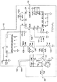
図1〜16は、ジャイロスコープの制御電子回路10のブロック図および回路図である。回路10がどのように動作するかの概観を得るのは、すべてのループが閉じており、すべてがすでに動作しているものとすることから始めることができる。図1は全体回路10のブロック図である。図2〜14は種々の回路を示し、これらの回路は、各回路図を集結して電子回路10の回路図を得ることができるように、それらの間に識別可能な結線を有する。回路10の構成が図1に示されているが、図17の回路210など、本発明を実施するために使用できるその構成の変形形態があり得る。
1 to 16 are a block diagram and a circuit diagram of the control
図2では、モータピックオフ信号が入力端21(J5)に入り、これを図2のモータ復調器回路20の増幅器22(U24)によって増幅することができる。増幅器23(U25)は、この信号が反転したものを供給することができる。この信号は、同期復調器として働くデバイス24(U10)へ行くことができ、デバイス24の下半分は、位相ロックループにおいて位相検出器として働いている。信号25(G)および26(H)は、直交復調用の直交スイッチング信号を供給することができる。デバイス24の出力は、増幅器27(U15D)へ行くことができる。出力28は、位相ロックループにおけるループフィルタとして働く増幅器29(U14A)へ行くことができる。増幅器29は、図3のデジタルPLL回路30のものでよい。増幅器29は積分器でよいので、モータの周波数が電圧制御発振器の自走周波数と同じではない場合でも定常状態位相誤差がないような位相ロックループとすることができる。増幅器29(U14A)の出力は、デバイス31(U4)において電圧制御発振器に影響を及ぼす電圧にすることができる。デバイス31(U4)それ自体を位相ロックループとすることができるが、使用されるすべてがデバイス31のVCOでもよく、したがってデバイス31が位相ロックループとして働いていないこともある。このVCOの出力32は、図4の復調器制御回路34のデバイス33(U1)のクロック周波数を制御することができる。デバイス33は、すべてのスイッチング周波数を発生することができる。したがって、モータ駆動信号に位相誤差がゼロで位相ロックされたモータ駆動周波数のスイッチング信号と、そのモータ駆動周波数の半分の周波数のスイッチング信号との完全な一組のスイッチング信号があり得る。
In FIG. 2, the motor pickoff signal enters the input 21 (J5) and can be amplified by the amplifier 22 (U24) of the
デバイス24(U10)の上半分は再び、モータピックオフからの信号を復調することができるが、この復調は同相でよく、したがってモータ駆動信号の大きさを表すDC信号を発生することができる。コンピュータが図5の主制御36のデバイス35(U21)(すなわち制御マイクロコントローラ)にデータを送出し、マイクロコントローラ35が図6のAGC制御38のD/Aコンバータ37(U12)にデータを送出して、D/Aコンバータ37の出力39を2ボルトにすると想定することができる。増幅器41(U14D)は、抵抗42(R63)を通る(D/Aコンバータ37からの)電流と、抵抗43(R94)を通る(回路20の同相復調器からライン44経由の)電流とを比較することができる。この電流が等しくなく反対でない場合には、増幅器41(U14D)の出力が変化する。これはまた、増幅器45(U17A)の出力端46の電圧も変化させ、それによって図7の回路48の電圧制御増幅器(VCA)47(U8)の利得が変化することになる。したがって正弦波発振器からの信号は、サインフィルタ49、ライン52を介した図8のモータ駆動出力端51、開始/実行選択回路53のデバイス59(U11A)、および増幅器54へ行く前に、VCAによって調整することができる。したがってAGCシステム38は、モータ復調器回路20の入力端21において特定の振幅のモータピックオフ信号を見ることを要求し、この振幅が得られるまでVCA48を調整することができる。
The upper half of device 24 (U10) can again demodulate the signal from the motor pickoff, but this demodulation may be in phase and thus generate a DC signal that represents the magnitude of the motor drive signal. The computer sends data to the device 35 (U21) (that is, the control microcontroller) of the
出力端51(J6)のモータ駆動信号は、ライン55を経由し、図9の位相検出器57の増幅器56(U17C)によって反転することができ、デバイス58(U11B)が別の復調器として動作することができる。デバイス33(U1)が、モータ駆動周波数の2分の1の周波数のスイッチング信号IおよびJをデバイス61(U3)を介して供給することができる。この復調器は、第2の位相ロックループ内の位相検出器として動作することができる。図9のサインPLLループフィルタ回路63の増幅器62(U14C)は、この位相ロックループのループフィルタとすることができ、また、定常状態位相誤差がゼロであるようなものを有することもできる。このループフィルタの出力64は、正弦波発振器65の周波数を制御することができる。他のPLLを用いた場合には、その正弦波は、復調器からのスイッチング信号に直交してロックすることができる。デバイス33(U1)は、この直角位相関係を考慮し、入力端21のモータピックオフからの信号と適切な関係をもつモータ周波数の2分の1の周波数の正弦波が得られるように位相調整されたスイッチング信号を発生することができる。
The motor drive signal at the output 51 (J6) can be inverted by the amplifier 56 (U17C) of the
レート信号は入力端66(J14)に入り、図11のレート復調器回路68の増幅器67(U22)によって増幅することができる。増幅器69(U18)は、この信号が反転されたものを供給することができる。デバイス71(U9A)は、入力端21のモータピックオフ信号に対して行われたように、同相復調でも直交復調でも同期復調器として動作することができる。デバイス75(U2)からの信号CおよびDは、直交復調用の直交スイッチング信号を与えることができ、ライン76上の復調された信号は、増幅器77(U15B)を経由し積分器72(U14B)を通って進み、図12の直交復調器(quad demod)74の出力端73(J4)にモータバイアス信号を与える。デバイス75(U2)からの信号AおよびBは、レート復調用の同相スイッチング信号を与えることができ、デバイス71(U9A)からのライン78上の復調信号は、増幅器79(U15A)を経由し増幅器81(U26)を通って進み、図13のレートフィルタ回路83の出力端82(J3)にレート出力信号を与えることができる。
The rate signal enters input 66 (J14) and can be amplified by amplifier 67 (U22) of
入力端21(J5)からの増幅されたモータピックオフ信号は、増幅器22(U24)の出力端を出て、Q信号として図14の開始検出器回路85の比較器84(U5)へ行く。比較器84(U5)は、その信号を方形波に変換し、これはライン86および87を介してマイクロコントローラ35(U21)に行き、それによってマイクロコントローラは、疑似方形波駆動信号を同期させ、次いでその信号を適切な振幅にまで駆動することができる。ダイオード88(D1)が付随する回路網は、増幅器22(U24)からのモータピックオフ信号の振幅と関連するDC信号を与えることができる。マイクロコントローラ35(U21)は、それが適切なレベルを検出したとき、正弦波駆動に切り換えることができる。
The amplified motor pickoff signal from the input 21 (J5) exits the output of the amplifier 22 (U24) and goes to the comparator 84 (U5) of the
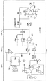
以下は、ジャイロスコープ制御電子回路の全体回路の様々な部分の細部についての説明である。図11のレート復調回路68に関して、その信号は、増幅器67(U22)の非反転入力端にAC結合することができる。その利得は、1μFのコンデンサ92(C56)のインピーダンスが抵抗91(R16)のインピーダンスと比べて非常に低いので、抵抗89(R2)と抵抗91(R16)の比(すなわち、20kΩ÷5.1kΩ)に1を加えたものとしてよい。コンデンサ92(C56)は、増幅器67(U22)の利得をDCで1に等しくするためにあり、したがって出力オフセットは、主として入力オフセット電圧によって決まり得る。信号レベルが低いセンサを使用する場合に、この段での利得を増大させたいことがあり、また、非常に大きな利得が使用されるべき場合には、補償作用が働かない演算増幅器に切り換えたいこともある。
The following is a detailed description of the various parts of the overall circuit of the gyroscope control electronics. With respect to
図13のレートフィルタ83は、3次バターワースフィルタとしてよい。回路図は、本来の23.5Hzの遮断周波数用の構成部品を示すが、250Hzの帯域幅が必要な場合もある。帯域幅を235Hzまで拡大するには、100kΩの抵抗93(R59)、94(R61)、および95(R62)をそれぞれ10kΩの抵抗と置き換えればよい。代わりに、10kΩの抵抗をそれぞれ100kΩの抵抗93、94、および95の上に(すなわち並列に)取り付けて、258Hzの帯域幅を得ることもできる。
The
直交復調器74は積分器とすることができ、これは、出力端73のモータバイアスを、レートチャネルからの復調直交信号にDC成分がなくなるまで調整する。この積分器の周辺の構成部品は、高速応答および適切な減衰応答が得られるように選択することができる。その総合的な効果は良好に見えるが、望ましくない量のAC信号がモータバイアス信号上に認められることがあり、したがって4.7MΩの抵抗96(R102)の両端間にコンデンサを配置することもある。470〜1000pFの値がよいはずである。復調信号はまた、最もよく知られている目的のために3極低域通過フィルタを通過し、直交出力端97(J13)へ行くが、直交零ループがアクティブのときには直交出力端が接地されているので、興味の対象ではない。第1の極77(U15B)は、直交零ループを不安定にする可能性のある位相シフトが加わらないように、高い周波数(733Hz)にすることができる。こうすると、第1の極があまり働かないので、このフィルタを2極フィルタのように働かせることができる。このことにより、その2次部分を適正に設定できなくなることがある。というのは、2次部分が利得ピークをもつからであり、この利得ピークは、抵抗98(R107)の値を10kΩから17.4kΩに増大させることによって除去することができる。100kΩの抵抗99(R109)および101(R110)は、9.5kΩの抵抗と置き換えて248Hzの帯域幅を与えることができるが、10kΩの抵抗を使用すると235Hzを与え、10kΩの抵抗をそれぞれ100kΩの抵抗99および101の上に(すなわち並列に)置くと、レートフィルタ83の場合のように258Hzを与えることができる。
The
開始検出器回路85は、モータピックオフ信号(増幅器22からのQ信号)から方形波をつくり、この方形波をライン86および87を介して主制御回路36のデバイス35に供給することができ、したがってデバイス35は、その疑似方形波駆動信号をモータピックオフからの信号に位相ロックすることができる。比較器84は、発振を防止するためのACヒステリシスを有することができ、(100pFのコンデンサ102(C69)を削除することによって)DCヒステリシスを使用する場合に発生することがある位相シフトを引き起こすことはない。ダイオード88(D1)を含む回路網を使用して、モータピックオフ信号Qの振幅を表すDC信号を生成することができる。AGC制御回路38のジャック103(J12)のモータ振幅出力が同じことを行うことができるが、ダイオード回路網は、開始モードにおいてすべてのループがロックされていないときに働かなければならない。
The
図5の主制御回路36は、18.432MHzの水晶104によって動作する16F876Aマイクロコントローラ35(U21)を有することができる。この周波数はその高調波が、10kHzのセンサを使用する場合に他のマイクロコントローラが動作する周波数である4MHzの高調波から離れるように選択することができる。主制御36から復調制御34へ行くいくつかの信号があり得る。開始/実行制御は、復調制御34に、復調制御34が制御支配をもつ開始/実行選択53の一部分に復調制御34がどのように対処しているべきかを伝えることができる。左/右制御は、左または右のピックオフ信号どちらかに対処する復調器のいくつかでどちらの極性を使用すべきかを復調制御に伝えることができる。またサイクルモードラインは、サイクルスキッピング法を使用すべきか否かを復調制御に伝えることができる。主制御36はまた、開始/実行選択53の一部分を制御することもできる。開始モードでは、マイクロコントローラ35のRA2の出力(L)は、疑似方形波駆動信号をモータ駆動増幅器(U17B)に接続し、この同じ信号は、+5ボルトを5.1kΩのプルアップ抵抗105(R22)に供給することができる。これは、回路が開始モードにあるときだけ比較器84(U5)の出力をアクティブにすることによって回路基板上のノイズを低減するために行うことができる。マイクロコントローラ35の出力RB0およびRB1を使用し、これらの出力を両方低、別々、または両方高のいずれかにすることによって、疑似方形波駆動信号を生成することができる。出力RB0およびRB1は、それぞれ100kΩの抵抗108(R68)および109(R69)を介してライン106に接続することができ、このライン106は、0.1μFのコンデンサ110(C55)を介して増幅器54と、開始/実行選択回路53のデバイス111(U11A)へと行く。これは3レベルの波形を与えることができ、この波形は、増幅器54(U17B)によって増幅されたときに大きくなりすぎないように、20kΩの抵抗107(R15)(U17Bのそば)によって減衰される。疑似方形波駆動信号の周波数は、マイクロコントローラ35上のEEPROMレジスタのうちの1つの内容によって決定することができる。この周波数は、4,608,000/[4×(番号+22)]とすることができるが、周波数を変更するオプションを使用した場合にはソフトウェアが事態を理解するので、これを知っておく必要は必ずしもない。主制御36は、デバイス112(U20A)の4つのスイッチを開くか閉じるかを決定することができ、これによりスイッチ113のデジタルPLL30のループ、スイッチ114のサインPLLループフィルタ63のループ、スイッチ115の直交復調74のループ、およびスイッチ116のAGC制御38のループがアクティブであるかアイドリングであるかが決まる。
The
復調制御34は、デバイス31からのライン32に沿って電圧制御発振器からの周波数を取り込み、モータピックオフ(21)周波数およびモータ駆動(51)周波数両方の復調器用制御信号を発生する。主制御36から来る3つの信号があり得る。開始/実行制御は、復調制御に、復調制御が制御支配をもつ開始/実行選択の一部分に復調制御がどのように対処しているべきかを伝えることができる。左/右制御は、左または右のピックオフ信号どちらかに対処する復調器のいくつかでどちらの極性を使用すべきかを復調制御に伝えることができる。またサイクルモードラインは、サイクルスキッピング法を使用すべきか否かを復調制御に伝えることができる。主制御36はまた、開始/実行選択53の一部分を制御することもできる。I2Cバスを使用して各マイクロコントローラ間の通信のための対応をすることができる。1つの可能な使用法は、クロックと制御信号の間の分割比を設定することである。たとえこの機能を使用しても、I2C手法を使用するためではなく4つの分割比のうちの1つを選ぶために、2つのデジタルラインとしてそのピンを使用するだけのこともある。
AGC制御38に関し、モータピックオフ(21)信号の同相復調は、モータ駆動信号の振幅を表すDC電圧を増幅器117(U15C)の出力44に与えることができる。この信号は、さらにフィルタリングし、出力端103(J12)(MTR増幅器出力)へ送出することができる。この信号はまた、抵抗43(R94)に電流を流すこともでき、増幅器41(U14D)がこの電流を、DAC37からのライン39に沿って抵抗42(R63)を通ってくる電流と比較する。積分器41(U14D)出力は、コンピュータによって設定できる所望の振幅に等しい感知振幅を得るためにそれが行かなければならないどこへも行くことができる。主制御36が積分器41の両端間のスイッチ116を閉じると、その出力は約0ボルトになり、したがって増幅器45(U17A)の出力は、抵抗118(R100)と抵抗119(R5)によって決定することができる。その値は、AGCがアクティブでないときに、信号MによってVCA48の利得を適切にするように選ぶことができる。これは、異なるセンサに変わるようなものである。たとえば、その利得がセンサをオーバドライブする場合には、ループがロックし各部分を動作させることが困難になることがある。
With respect to the
モータ復調器20に関し、モータピックオフ入力端21からの信号は、増幅器22(U24)の非反転入力端にAC結合することができる。その利得は、1μFのコンデンサ123(C59)のインピーダンスが抵抗122(R19)のインピーダンスと比べて非常に低いので、20kΩの抵抗121(R4)と5.1kΩの抵抗122(R19)の比(すなわち、R4/R19)に1を加えたものとしてよい。コンデンサ123(C59)は、増幅器の利得をDCで1に等しくするためにあり、したがって出力オフセットは、主として入力オフセット電圧によって決まり得る。信号レベルが低いセンサを使用する場合に、この段での利得を増大させたいことがあり、また、非常に大きな利得の場合には、補償作用が働かない演算増幅器に切り換えたいこともある。
With respect to
デジタルPLL30に関して、増幅器29(U14A)は、デジタルPLL用のループフィルタとすることができる。デバイス112(DG412)のスイッチ113がループフィルタの両端間で閉じると、出力を接地することができる。その場合、電圧制御発振器31(U4ピン9)の入力端へのライン124に沿った電圧は、上部の2.8kΩの抵抗125(R105)と20kΩの抵抗126(R6)との直列結合、ならびに下部の10kΩの抵抗127(R41)と100kΩの抵抗128(R66)との並列結合によって形成される減衰器によって決めることができる。復調制御34のコードは、モータピックオフ周波数が約10kHzである場合に、デバイス31のVCO周波数が約4MHzになるように書くことができる。センサ周波数が大幅に変わる場合、対応は、復調制御のコードを変更することになり得る。これは不便なこともあるので、周波数の大幅な変更を行うには85pFのコンデンサ129(C85)の値を変更するだけ、また軽微な調整を行うには抵抗127(R41)の値を変更するだけという可能性の方が高い。74HC4046Aチップは、デバイス31の74HC4046チップとは異なる特性を有する。Aバージョンの方が高速であり、したがって、より高い周波数のセンサに対応するのに単純にそれを高速にしたいこともある。別の選択肢は、1.96kΩの抵抗131(R104)の値を変更することにより周波数を変えることでもよい。こうすることは、入力端の電圧を電圧範囲(すなわち2.5ボルト)の中心付近にしておくのがよいために、入力端の電圧分割器回路網について検討するよりも都合がよいこともある。
Regarding the
正弦波発振器65は、3段位相シフト発振器とすることができる。それぞれが60°の位相シフトを与える3つの位相シフト段132、133、134と、180°の位相シフトを与えるインバータ135とがあればよく、必要に応じループまわりで合計が360°になる。段132、133、134、および135は、LM13700チップを利用することができる。これらの相互コンダクタンス増幅器は、電流制御抵抗のように動作することができる。第1段132では、ライン136(ピン16)への電流が、ライン138(ピン13)とライン139(ピン14)の間の差動電圧に相関してライン137(ピン12)からの電流の利得を制御することができる。1000pFのコンデンサ176(C64)が電流制御抵抗と共に作用して、60°の位相シフトを有するRC低域通過部を形成することができる。ダーリントントランジスタ対141が信号をバッファリングすることができ、したがって各段は互いに負荷をかけない。第1段132からの信号は、ライン142から整流器143へ行くことができ、積分器144(U16B)は、整流器143の平均DC出力と、470kΩの抵抗145(R103)と30kΩの抵抗146(R98)が与える約0.3ボルトの基準電圧とを比較し、次いでその誤差電圧を積分することができる。積分器144の出力は、ライン147を介して位相シフト発振器の反転段135で利得を制御することができ、そうして正弦波の振幅は、歪みを最小限にするためにかなり低いレベルに制御される。正弦波発振器65は、PLL回路63がその非ロック状態にあるときにはモータ駆動周波数で発振するように設定することができるが、こうするのは、積分器の両端間のスイッチ114が閉じられたために増幅器148(U14C)の出力が接地されているときである。発振器65の周波数は、コンデンサ137(C64)、コンデンサ149(C65)、およびコンデンサ151(C66)の1000pFの値を変更することによって(ただし各値を等しく保ちながら)、あるいは抵抗152(R82)、抵抗153(R83)、および抵抗154(R84)の51kΩの値を変更することによって(ただし各値を等しく保ちながら)、調整することができる。ライン136(ピン16)またはライン155(ピン1)に入る電流の最大定格は約2mAである。これらの部分は非常に壊れやすく、2mAではそれらを破壊するおそれがある。それらには1mAでさえも通すべきではない。抵抗152(R82)に51kΩを使用すると、電源がライン136(ピン16)の中に通し得る最大電流は約0.5mAになり、これは妥当と思われる。周波数を倍にするには、各コンデンサの値を半分にすればよい。発振器65の周波数は(アイドリング時に)、位相ロックループが迅速かつ確実にロックするように、モータ周波数に近くなければならない。
The
VCA48は、デバイス47にLM13700相互コンダクタンス増幅器を使用することができる。20kΩの抵抗156(R14)は、線形化ダイオードにバイアスをかけて歪みを低減させることができる。51kΩの抵抗157(R86)を通る電流は、ライン159(ピン3)とライン161(ピン4)の間の差動電圧に対して、ライン158(ピン5)から出る電流の比率を制御することができる。100kΩの抵抗162(R73)は、その電流を電圧に変換することができ、この信号は、トランジスタ164によってバッファリングすることができる。トランジスタ164は、V+に接続されたコレクタと、10kΩの抵抗163(R57)を使用して−12ボルトにバイアスされたエミッタとを有する。
VCA48の出力165は、サインフィルタ49へ行くことができる。サインフィルタ49は、正弦波の歪みを低減させることができる。演算増幅器166(U16D)は、必要な信号反転を行うために使用され、100pFのコンデンサ167は、フィルタの第1の極を得るために162kΩの帰還抵抗168(R96)の両端間に配置されたものである。抵抗169(R54)および171(R55)は同じ10kΩの値を有し、この比率は、異なるセンサに対応するために周波数が変更されるならば変わることがない。7.5kΩの抵抗172(R91)は抵抗173(R92)とほぼ等しく、0.0022μFのコンデンサ174(C77)はコンデンサ175(C78)とほぼ等しい。構成部品の値から、フィルタは10kHzの帯域幅に設定することができるが、この帯域幅は、10kHzセンサが5kHzの駆動周波数を有するので調整されることもある。いくつかの構成部品の値は変更することができ、あるいは、2次高調波の80dB抑制を達成できないかもしれないと考えて、サイクルスキッピングのオプションを基礎設計にすることもできる。80dBという(仕様に要求された)2次高調波抑制を達成することは困難なことがある。発振器が自走しているときに、これだけの抑制を正弦波発振器65およびサインフィルタ49が達成できるとしても、ひとたび正弦波位相ロックループがロックすると、スペクトル純度が維持できなくなることがある。これは、ループフィルタの出力が、周期内で周波数に影響を与えようとすることによって波形に影響を及ぼすことがあることによる。電圧制御発振器への入力端でAC信号のすべての痕跡をフィルタで除去しようとすると、位相ロックループの制御ができなくなり、ループは適切にロックすることができないことがある。これが、サイクルスキッピングのオプションを含めることの動機となったものである。このオプションがひとたびアクティブ化されると、レート信号が復調されているときに正弦波駆動信号が存在しなくなるので、歪みは無関係になり得る。
The
開始/実行選択回路53に関して、Lと名づけた信号は、それがどんなものとも同期されないようなので、主制御36から来る。Kと名づけた信号は、復調制御34により供給されるデバイス61のラッチから来ることができる。連続モードがもっぱら使用されるなら、信号Kは、実行モードになっていることを示す定常信号にすぎないので、これらのラッチから信号Kが来なくてもよい。しかし、レート信号が復調されているときに駆動信号を無効にするためにサイクルスキッピングモードが使用される場合に、信号Kは駆動信号と同期して使用されるので、ラッチから信号Kが来ることもある。スイッチの「オン」抵抗は、信号レベルと関係することがあり、この抵抗は、抵抗107(R15)と共に作用して電圧分割器として働くことができる。スイッチ抵抗が抵抗107(R15)の20kΩの値と比べて低いので、その出力は入力と非常に近くなり得るが、スイッチ抵抗が信号レベルに関係するということは、開始/実行選択回路に供給する正弦波がたまたま完全であったとしても、歪みを発生させる機構をもたらす可能性がある。このことが、歪みの心配がないサイクルスキッピングモードを使用することの別の動機になり得る。
With respect to the start /
位相検出器57は、モータ復調回路20およびレート復調回路68に使用されている復調器と同じ種類とすることができる。こうしてよい理由は、制御信号とスイッチの応答(開または閉)との間に遅延があり得ることである。デジタルPLL回路30では、そのループフィルタは、デジタルPLL内の復調器からDC電圧が来ないようにする。こうするために、マイクロコントローラへのクロックは、入力端21のモータピックオフ信号に対し周波数をロックすることができ、また、スイッチ内の遅延を補償するために、自動的に位相を進めることもできる。両方のPLLにおいて同じスイッチ、および同じ復調器を使用していることがあるので、スイッチング信号のタイミングは、モータピックオフ信号に対して正弦波が適正に位置決めされることになるように、正弦波PLLのスイッチ内の遅延を考慮に入れることができる。そのタイミング誤差は、2つの異なる位相ロックループにおいて完全に異なる種類の位相検出器が使用されたかのように絶対的な遅延と関連するのではなく、各スイッチの遅延の差と関連するはずである。
The
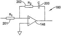
図9のサインPLLループフィルタ63に関して、位相ロックループが実際に設計されなければならない。制御ループをおおまかに調整するだけで、それを適切に動作させることはできない。しかし、本質的な要素は、差動増幅器148、抵抗201(R1)、抵抗202(R2)、およびコンデンサ203(C)を組み込む図15の回路図180と共に明らかと思われる。入力が抵抗201を通り、増幅器200の非反転入力端へ行く。増幅器の反転入力端は、グランドまたは基準端子に接続することができる。直列に接続されたコンデンサ203と抵抗202を組み込む、増幅器の出力端から増幅器の非反転入力端への帰還ループがあってもよい。KΦは、単位が電圧/ラジアンの位相検出器変換利得とすることができる。K0は、単位がラジアン/秒/ボルトのVCO変換利得とすることができる。式「ωn=((K0・KΦ)/(R1・C))1/2」および「R2=2/(C・ωn)」を使うことができる。KΦおよびK0は測定することができ、R1およびωnの妥当な値は選ぶことができる。CおよびR2は、それぞれ第1式および第2式を使って計算することができる。この手法は、減衰定数が1であるとしている。減衰は、式「ζ=(R2・(C/2))・ωn」によって計算することができる。R2があまりに低い場合、ループは減衰不足となり、不安定になることがある。R2があまりに高い場合、不必要に大きなAC信号が正弦波電圧制御発振器に供給されることがあり、それによって歪みが生じる。
For the sine
最初の配置、および構成部品の値は、ブレッドボード手法に基づくものでよい。全般的な改変が、ブレッドボードから正規のボード手法に移行したことの結果として実施されることがある。これらの変更は、動作周波数にかかわらずすべての基板に加えられるべきである。これらの変更は、ブレッドボード上でどのようにして物事が行われたかということから、ブレッドボード段階の次にどのようにして物事が行われるかへ転換するための、ほとんどが軽微な調整であり得る。 Initial placement and component values may be based on a breadboard approach. General modifications may be implemented as a result of the transition from breadboarding to regular boarding practices. These changes should be made to all boards regardless of the operating frequency. These changes are mostly minor adjustments that translate from how things are done on the breadboard to how things are done after the breadboard stage. obtain.
その変更は、抵抗118(R100)を14kΩに変更すること、+5ボルトとDAC37(U12、ピン3)のZ信号端子との間に20kΩのプルアップ抵抗を配置すること、抵抗127(R41)(デジタルPLL30において)の値を20kΩに変更すること、248Hzの帯域幅を得るために抵抗93(R59)、94(R61)および96(R62)を9.5kΩの値に変更すること、抵抗98(R107)を17.4kΩの値に変更すること、248Hzの帯域幅を得るために抵抗99(R109)および101(R110)を9.5kΩの値に変更すること、および抵抗96(R102)の両端間に470pFのコンデンサを配置することを含むことがある。 The change is that the resistor 118 (R100) is changed to 14 kΩ, a 20 kΩ pull-up resistor is arranged between +5 volts and the Z signal terminal of the DAC 37 (U12, pin 3), and the resistor 127 (R41) ( Changing the value of the digital PLL 30) to 20 kΩ, changing the resistors 93 (R59), 94 (R61) and 96 (R62) to 9.5 kΩ to obtain a bandwidth of 248 Hz, Changing R107) to a value of 17.4 kΩ, changing resistors 99 (R109) and 101 (R110) to a value of 9.5 kΩ to obtain a bandwidth of 248 Hz, and both ends of resistor 96 (R102) It may include placing a 470 pF capacitor in between.
次の一連の改変は、周波数特性とすることができる。第1の基板上で、正弦波発振器65を5kHz近くでアイドリングするためにコンデンサ137(C64)、149(C65)および151(C66)の値を2,200pFに変更することができる。アイドリング周波数は、ループをロックさせるために動作周波数にかなり近くなければならない。この周波数を高くするには、コンデンサの値を小さくすればよい。微調整のためには、抵抗152(R82)、153(R83)および154(R84)の値を一致させて変更することができるが、元の51kΩより小さくすべきではない。デバイス31(U4)の74HC4046Aチップのアイドリング周波数は、コンデンサ129(C85)の値を変更することによって調整することができる。この周波数は、抵抗131(R104)の値を変更することによって微調整することができる。サインフィルタ49の周波数は、抵抗168(R96)、172(R91)および173(R92)の値を同じ率で変更することによって調整することができる。最初の値はおおまかに10kHzに設定された。
The next series of modifications can be frequency characteristics. On the first substrate, the values of capacitors 137 (C64), 149 (C65) and 151 (C66) can be changed to 2,200 pF to idle the
図16は、本発明の回路に種々の電圧を供給する回路を備えた電源177を示す。回路178は、デバイス112(U20A)(DG412)に使用できるデカップリングを実現することができる。
FIG. 16 shows a
図2〜14の回路には、図中で文字A、B、C、D、E、F、G、H、I、J、K、L、M、Q、X、YおよびZで名づけた信号、ならびに数字28、32、44、52、55、64、76、78、86、87、106、181、182、183、184、185、186、187、188、189、191、192、193、194、195、196および197で名づけた相互接続ラインによって示される様々な相互接続があってよい。
The circuits of FIGS. 2-14 include signals named A, B, C, D, E, F, G, H, I, J, K, L, M, Q, X, Y and Z in the figure. , As well as the
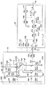
図17は、本発明を実施する別の回路210のブロック図である。回路210は、モータ駆動用の高純度正弦波を使用して、ジャイロスコープ100の制御システムのノイズレベルを低減することができる。モータピックオフ信号212がジャイロ100から来て、同期モータ復調器211へ行くところから始めることができる。直交出力213を与えるモータ復調器211は、位相ロックループ(PLL)内の位相検出器として動作することができる。この位相検出器から、信号はループフィルタ214を通り、次いでデジタル電圧制御発振器215へ行くことができ、この発振器は、復調器信号を供給するマイクロコントローラ(復調器制御)216用のクロック信号を与える。復調器211と、ループフィルタ214、およびVCO215との組合せが、位相ロックループとして動作することができる。これは、ループフィルタ214が積分器であるので、モータの周波数が電圧制御発振器215の自走周波数と同じでなくても定常状態位相誤差のないような位相ロックループになり得る。(この場合の自走周波数は、積分器が短絡されたときに存在する周波数と考えることができ、この短絡は、主マイクロコントローラ221が準備できるものである。)したがってマイクロコントローラ216は、スイッチ内の遅延を補償さえする、ほぼ完全な一組の復調器信号を供給することができる。モータ復調器211の同相出力217は、モータ駆動信号238の振幅を表すDC信号を生成することができる。自動利得調整(AGC)218は、復調器からのDC信号を、主マイクロコントローラ221が調整するデジタル−アナログ変換器(DAC)219からのDC信号と比較することができ、その差の積分を使って電圧制御増幅器(VCA)222の利得を変化させることができる。その場合、正弦波発振器223からの信号は、サインフィルタ224およびモータ駆動器225へ行く前に、VCA222によって調整することができる。したがって、AGCシステム218は、モータピックオフ信号212の特定の振幅を見ることを要求し、次に、この特定の振幅が得られるまでモータ駆動信号238の振幅を調整することができる。
FIG. 17 is a block diagram of another
感知ピックオフ信号237は、ジャイロ100から来て、同期レート復調器(レート復調器)226へ行くことができる。直交復調は、モータバイアス信号239を与えるために、積分器228を通って進む信号227を供給する。同相復調229は、フィルタ231によってフィルタリングされると出力241になる信号を与え、この信号はジャイロ100の回転レートを表す。
The
正弦波モータ駆動信号238を生成するために、別の位相ロックループを使用することができる。復調器制御216は一組のスイッチング信号を供給し、この信号の周波数は、復調器211、226、232に使用されるスイッチング信号の周波数の2分の1、または他の分数倍の周波数である。このスイッチング信号はまた、他のスイッチング信号との適切なタイミング関係も有し、その結果、モータ駆動用に生成される正弦波が、ジャイロ100から来る信号と適切な関係をもつようになる。正弦波復調器232と、ループフィルタ234、および正弦波VCO223とは、この第2の位相ロックループを構成することができる。
Another phase-locked loop can be used to generate the sinusoidal
モータピックオフからの信号212はまた、整流器235および低域通過フィルタ236へ行き、次いで、主マイクロコントローラ221のアナログ−デジタル変換器へも行くことができる。起動中に整流器回路235を使用して、位相ロックループが適切にロックするのに十分な振幅に信号が増加したときを検出することができる。起動するために、主マイクロコントローラ221は、正弦波をモータ駆動器225に接続するのではなく、主マイクロコントローラ221からの信号をモータ駆動器に接続するために、(主マイクロコントローラによって制御することができる)別のマイクロコントローラに、デジタル信号を波形選択スイッチ224へ送るように命令することができる。次いで、主マイクロコントローラ221は、3レベルを有する信号であり、3レベルを使用する場合にだけ可能な程度に正弦波に似ている信号を生成する。アルゴリズムを使用して、周波数が異なる一連のトーンバーストでセンサを刺激することができる。ジャイロ100内のプルーフマスがひとたび振動を開始すると、比較器がその信号を方形波に変換することができ、主マイクロコントローラ221は、この方形波を同期用に使用することができる。モータ駆動信号238の位相をモータピックオフ信号212に対して適切に調整することによって、マイクロコントローラは、かなりの振幅までセンサを駆動することができる。次いで、主マイクロコントローラ221は、信号の周波数を測定し、この情報を使用してモータ駆動信号238のパルス幅を調整することができる。位相もパルス幅もセンサの周波数に理想的に適合されていると、主マイクロコントローラ221は、適切な大きさの振幅までセンサを駆動することができる。次いで、マイクロコントローラ221は、両方の位相ロックループをロックし、他のマイクロコントローラに対し、波形選択スイッチ224を使用して正弦波駆動に切り換えるように命令することができる。
主マイクロコントローラ221が波形選択スイッチ224自体を制御するのではなく、他のマイクロコントローラに対し制御するように命令するのは、波形選択スイッチ224に別の用途があるためである。この別の目的のために、主マイクロコントローラ221は、波形ではなくグランドのDCレベルを与えることができる。その場合、波形選択回路224を使用して、正弦波とグランドのどちらかをモータ駆動信号238の交番周期で選択することができ、これが、主マイクロコントローラ221からではなく復調制御216から最終的に波形選択信号が来る理由である。主マイクロコントローラは、他のマイクロコントローラにこの動作モードをいつ使用するかを命令できるが、他のマイクロコントローラは、このモードを使用するようにひとたび命令されると、サイクルスキッピング信号と共にすべての復調信号を生成することができる。こうするのは、モータ駆動信号238の波形の2次高調波が、レート復調器226によってレート出力信号にエラーをつくり出すようにして復調される可能性があるためである。この問題は、モータ駆動器225がオフであるときだけレート復調器226が信号237を復調するので、解消することができる。この機能がないと、モータ駆動238の波形の2次高調波抑制に対する要件が非常に厳しいので、そのような抑制を確実に達成することは困難になり得る。
The
図18のMEMS振動ジャイロスコープ(または機械振動子)250への駆動波形は一般に、そもそも正弦波ではなかった。加えて、ジャイロのプルーフマスをその共振周波数の駆動信号で駆動しようとすることは、そのためのQの高い回路による多くのリンギングを伴う問題になり得る。さらに、感知レート251のピックオフを得るのは容易ではなく、また、たとえそうしたとしても識別するのは容易ではない。解決策は、ジャイロモータの10kHz振動レートに対し適切な位相の、位置合わせされた滑らかな5kHz正弦波を用いてジャイロモータ(すなわち、振動プルーフマスまたは機械振動子)250を駆動することであり得る。
The drive waveform to the MEMS vibration gyroscope (or mechanical vibrator) 250 in FIG. 18 is generally not a sine wave in the first place. In addition, attempting to drive a gyro proof mass with a drive signal at its resonant frequency can be a problem with many ringing due to the high Q circuit. Furthermore, it is not easy to obtain a pick-off of the
まず、モータ駆動信号253の同期信号に関し、モータピックオフ251に注目することができる。感知ピックオフ252は、地表または宇宙のある面に対するジャイロの回転レートを表す出力としてよい。
First, the motor pick-off 251 can be noted with respect to the synchronization signal of the
駆動信号253には滑らかな正弦波が必要であるが、これは発振器から得ることができる。この信号は、モータ周波数の2分の1、すなわち5kHzでなければならず、また10kHzのモータピックオフ信号251に位相ロックしていなければならない。またマイクロコントローラ254の命令クロックも、命令信号間のエッジがモータ駆動信号253のエッジまたは周期の末端で発生するように、モータピックオフ信号251にロックすることができる。各命令信号のエッジがそれぞれモータピックオフ信号の周期のエッジで発生するようにマイクロコントローラ254のクロックを制御する電圧制御発振器(VCO)があってよい。これは、ジャイロ250のプルーフマスにかかる駆動信号の静電圧力の最大効果を得るためのものである。
The
駆動信号253は5kHzの周波数でよく、ジャイロ250のプルーフマス振動の10kHzで感知信号と同期させて、発生する可能性のある2次高調波を最小限にすることができる。ジャイロを5kHzの正弦波253で駆動して、この正弦波を、発生する可能性のあるどんな2次高調波ともよりよく区別することができる。しかし、プルーフマスの両側のくし状駆動要素が互いに完全に同じではなく、その結果ジャイロ250のプルーフマスにかかる駆動力がわずかに非対称になるために、いかなる高調波もない純粋な正弦波でもなお、高調波の発生をもたらす可能性がある。
The
マイクロコントローラ254からの制御信号255は、感知信号252(ジャイロの回転レート情報を有する)がジャイロ250から読み込まれている間、ドライブ信号253のブランキングを可能にすることができる。ブランキングは、ゼロ出力にされている駆動信号253の1つまたは複数の周期を含むことができる。たとえば、1つおきの周期をブランキングすることができる。あるいは2つおきの周期をブランキングすることができる。マイクロコントローラ254は、任意の数の駆動信号をジャイロ250に許可するように、また任意の数の駆動信号253をブランキングするようにプログラムすることができる。スイッチ回路またはブランキング回路263は、信号選択器とみなすことができる。この信号選択器の少なくとも一部分がマイクロコントローラ254の外部にあってもよい。
The control signal 255 from the
5kHzは、駆動信号253の極性に対してジャイロ250の駆動機構を、ジャイロを駆動する吸引力に関して中立にできるので、よい周波数であり得る。
ジャイロのプルーフマスと、対応するモータピックオフ信号251との10kHz共振は、ジャイロの駆動および感知システムのための主クロックとみなすことができる。感知ピックオフ信号252は、ジャイロの回転レートの大きさを示す振幅を有することができる。したがって非回転時には、振幅は理論的にゼロになり得る。したがって、非常に小振幅の信号の大きさを妥当な精度で求める必要があり、駆動信号253は、感知ピックオフ信号252の読込み中にはブランキングされなければならない。
5 kHz can be a good frequency because the drive mechanism of the
The 10 kHz resonance of the gyro proof mass and the corresponding
ジャイロの駆動および感知用システム10は本質的にアナログであるが、デジタル化することができる。デジタル化には、モータピックオフ251および感知ピックオフ252からのアナログ入力を受け取るためのアナログ−デジタル変換器(ADC)が必要になることがある。そのデジタル処理は、24ビットの分解能によって96000サンプル/秒で信号を変換することができる。このデジタル化システムは、浮動小数点精度の正確さまでの動作ができ、デジタル信号プロセッサ(DSP)を用いて実施することができる。
The gyro drive and
位相ロックループ出力信号にいくつかの差周波数があることがあり、したがって、これらの周波数を除去しながらなお基本周波数を保持するフィルタが必要になることがある。また、周期内で信号の周波数を変更すると歪みを引き起こすことがあり、したがって周波数は、信号の周期のエッジまたは末端で変更または調整されなければならない。 There may be several difference frequencies in the phase-locked loop output signal, so a filter that removes these frequencies and still retains the fundamental frequency may be required. Also, changing the frequency of a signal within a period can cause distortion, so the frequency must be changed or adjusted at the edges or ends of the period of the signal.
コントローラ254からのスイッチング信号のうち、いくつかは10kHzとし、他は5kHzとすることができる。これらの信号は、1次主クロックとみなすことができるモータピックオフ252からの10kHz信号と「完全に」整合させることができる。
Of the switching signals from the
5kHz信号257は、第1のループ261から第2のループに供給することができる。第2のループ262は、5kHzの正弦波信号を供給する正弦波発振器と結びつけることができ、この5kHz正弦波は、第1のループ261からの5kHz信号にロックされ、あるいは「完全に」整合されている。
The 5
第1の位相ロックループの信号は、モータピックオフ信号251に合わせることができる。このループ261から、5kHzおよび10kHzのスイッチング信号が来てよい。5kHz信号257は、ジャイロを駆動するための正弦波信号253を与える第2の位相ロックループ262へ行くことができる。ブランキングは、回路の末端ではあるが信号253がモータ駆動入力端へ行く直前に入ってよい。ブランキングには、コントローラ254からの出力によってトリガをかけることができる。第1のマイクロプロセッサが、第1の位相ロックループと関連する第2のマイクロプロセッサに、スキップモードまたは非スキップモードを示す信号を送出することができる。次に、第2のプロセッサは、ジャイロからの感知信号252の読込み中の時間にドライブ回路をブランキングするために、信号255をブランキング回路263に供給することができる。
The signal of the first phase lock loop can be matched to the
第2のループ262からの正弦波信号253は、3段の低域通過フィルタによって滑らかになっていてよい。その出力はインバータを通り、次にその入力端へ、第2のループ内の正弦波発振器への帰還信号として行くことができる。
The sine wave signal 253 from the
主マイクロコントローラ254は、入ってくるモータピックオフ信号251と同期してスイッチを制御することができる。位相ロックループ出力信号257および253もまた、ピックオフ信号251と同期することができる。ここで同期しているとは、各信号のエッジが互いに整合し、また正弦波などのゼロ交差信号のクロスオーバ点と整合していることを意味してよい。たとえば、周波数の変更はエッジまたはクロスオーバ点で行わなければならない。全クロック周期または半周期の中間で変更または切り換えなければならないものは何もない。この手法により、各信号間のジッタを回避することができる。
The
電圧制御発振器は、位相ロックループ261および262の部品でよい。ループがロックすると、クロック信号は、ジャイロスコープからの入力モータピックオフ信号など重要な事象と整合させることができる。ピックオフ信号は、主クロック信号でよい。主コントローラ254のクロックは、ピックオフ信号251に合わせることができる。
The voltage controlled oscillator may be a component of phase locked
スイッチ遅延は、開であろうと閉であろうと補償することができる。これは、位相ロックループによって実現することができる。この方法では、第1の位相ロックループ261は、スイッチの平均遅延を補償することができる。マイクロコントローラまたは位相ロックループは、各方形波信号265および266でよい10kHzスイッチ信号および5kHzスイッチ信号を生成することができる。5kHz信号266は、第2の位相ロックループに入力することができる。第2の位相ロックループ262の出力信号253から生成された正弦波は、スイッチ信号と同期させ整合させることができる。
The switch delay can be compensated for whether it is open or closed. This can be achieved by a phase locked loop. In this manner, the first phase locked
それに続いて、5kHz信号265もまた、10kHz信号266と適切に整合させることができる(すなわち、同相であるのと同様だが、各波形の対応するエッジおよび/またはクロスオーバ点で整合させることもできる)。図19のように、信号265と266の各エッジは、互いに整合させることができ、また正弦波253のクロスオーバ点と整合させることができる。各信号の一方の波形の、他方の信号の位置との相対的な位置は、各信号が互いに適切に整合されているか否かを示すことができる。図17中で囲まれた第1のループの回路271は、図18のブロック図内のループ回路271に対応することができる。同様に、図17中で囲まれた第2のループの回路272は、図18のブロック図内の信号選択器を伴うループ回路272に対応することができる。
Subsequently, the 5 kHz signal 265 can also be properly aligned with the 10 kHz signal 266 (ie, similar to being in phase, but can also be aligned at the corresponding edge and / or crossover point of each waveform. ). As shown in FIG. 19, the edges of the
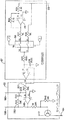
図20は、機械振動子250またはジャイロスコープ100の制御電子回路のデジタルバージョンを明らかにしている。ジャイロ100のモータピックオフ出力301は、デジタル信号プロセッサ(DSP)310のアナログ−デジタル変換器(ADC)312に接続することができ、このADCは、一例として、米国、マサチューセッツ州、NorwoodのAnalog Devices Inc.製のモデルADSP21262とすることができる。ジャイロ100の感知ピックオフ出力端302は、デジタル信号プロセッサ310のアナログ−デジタル変換器313に接続することができる。DSP310の、デジタル−アナログ変換器を含むモータ駆動出力端303は、増幅器305を介してジャイロ100のモータ駆動入力端に接続することができる。モータ駆動信号または振動子駆動信号は、デジタル的に生成した合成正弦曲線すなわち正弦波信号とすることができ、この正弦波信号は、モータまたは振動子の感知ピックオフ信号の分数倍周波数を有し、モータピックオフ信号と同期および/または整合されている。駆動信号は、要望に応じ他の波形でもよく、DSPによって生成することもできる。様々なスイッチングの遅延またはタイミングは、必要に応じデジタル的に補償することができ、あるいはDSPによって決めることもできる。DSP310のモータバイアス出力端304は、増幅器306を介してジャイロ100のモータバイアス入力端に接続することができる。DSP310とマイクロコントローラ308の間に接続された8ビットの双方向データバス307があってもよい。マイクロコントローラ308とコンピュータ311の間にRS232インタフェース接続309があってもよい。
FIG. 20 reveals a digital version of the
図21は、DSP310の回路図である。ジャイロ100のモータピックオフ信号出力301は、ADC312を介して乗算器316および317へ行くことができる。ジャイロ100のモータ感知ピックオフ出力302は、ADC313を介して乗算器318および319へ行くことができる。数値制御コサイン波発振器321は、乗算器318および316に接続された出力端を有することができる。数値制御正弦波発振器322は、乗算器317および319に接続された周波数出力端323を有することができる。乗算器317の出力は、ループフィルタ324へ行くことができる。ループフィルタ324の出力は、有限長インパルス応答(FIR)フィルタ325へ行くことができる。フィルタ325の出力は、数値制御コサイン波発振器321および数値制御正弦波発振器322へ行くことができる。
FIG. 21 is a circuit diagram of the
乗算器316の出力は、FIRフィルタ326へ行くことができる。フィルタ326は、差動増幅器328の入力端に接続されるモータピックオフレベル出力327を有することができる。また、差動増幅器への1つの入力は、基準レベル329とすることができる。差動増幅328の出力は、積分器331へ行くことができる。積分器331からの駆動レベル出力332は、可変利得増幅器333へ行くことができる。数値制御1/2周波数(または他の分数倍周波数)正弦波発振器334は、位相補償器335に接続された出力端を有することができる。位相補償器335の出力は、可変利得増幅器333へ行くことができる。可変利得増幅器の出力はDAC314へ行き、このDAC314はモータ駆動出力303を供給することができる。
The output of
乗算器318の出力は、FIRフィルタ336へ行くことができる。FIRフィルタ336は、直交零出力337を積分器338に供給する。モータバイアス出力339は、DAC315へ行くことができ、このDAC315は、増幅器306を介してジャイロ100にアナログモータバイアス出力304を供給することができる。乗算器319の出力は、FIRフィルタ341へ行くことができる。FIRフィルタ341は、レート出力342を与えることができる。
The output of
DSP310の数値出力は、データバス307およびインタフェース309を介してマイクロコントローラ308およびコンピュータ311にデジタルで伝達することができる。これらの出力は、周波数出力323、モータピックオフレベル327、駆動レベル出力332、4レベル出力337、モータバイアス出力339、およびレート出力342を含むことができる。
The numerical output of the
本明細書では、違った様態または時制で述べられているが、その内容には仮定的または予言的な性質のものもあり得る。
本発明を少なくとも1つの説明的な例に関して説明してきたが、本明細書を読めば多くの変形形態および改変形態が当業者には明らかになるであろう。したがって、添付の特許請求の範囲は、そのようなすべての変形形態および改変形態を含むように、従来技術を考慮して可能な限り広く解釈されるものとする。
Although described herein in different manners or tenses, the content may be of a hypothetical or prophetic nature.
Although the present invention has been described with respect to at least one illustrative example, many variations and modifications will become apparent to those skilled in the art upon reading this specification. Accordingly, the appended claims are to be construed as broadly as possible in view of the prior art to include all such variations and modifications.
Claims (28)
前記第1の位相ロックループの出力端に接続された第2の位相ロックループとを備え、
前記第2の位相ロックループは、前記機械振動子モータピックオフからの信号の分数倍周波数を有する正弦波信号を出力することができる、
機械振動子制御システム。 A first phase-locked loop connected to the mechanical oscillator pickoff;
A second phase locked loop connected to an output end of the first phase locked loop;
The second phase-locked loop can output a sine wave signal having a fractional frequency of the signal from the mechanical vibrator motor pickoff.
Mechanical vibrator control system.
前記第2の位相ロックループの出力端、および前記機械振動子の駆動入力端に接続されたスイッチとをさらに備える、請求項1に記載のシステム。 A demodulator connected to a mechanical oscillator sensing pickoff;
The system of claim 1, further comprising a switch connected to an output end of the second phase-locked loop and a drive input end of the mechanical vibrator.
前記スイッチが閉じられることにより、前記第2の位相ロックループは前記正弦波信号を前記機械振動子の駆動入力端に供給することができ、
前記スイッチが開放されることにより、前記復調器は、前記機械振動子感知ピックオフからの信号を読み込むことができる、請求項4に記載のシステム。 A controller connected to the demodulator and the switch;
When the switch is closed, the second phase-locked loop can supply the sine wave signal to the drive input of the mechanical vibrator,
The system of claim 4, wherein the demodulator is capable of reading a signal from the mechanical transducer sensing pickoff by opening the switch.
前記スイッチは、前記正弦波信号のエッジまたはクロスオーバ点で作動される、請求項6に記載のシステム。 A plurality of switches,
The system of claim 6, wherein the switch is activated at an edge or crossover point of the sinusoidal signal.
前記第1の周波数の分数であり、前記第1の信号に位相ロックされた第2の周波数を有する第2の信号を供給するステップと、
前記第2の信号に位相ロックされた正弦波信号を供給するステップと、
前記正弦波信号を前記機械振動子の駆動入力端に供給するステップとを含む、正弦波機械振動子制御の方法。 Picking off a first signal having a first frequency from the mechanical oscillator;
Providing a second signal having a second frequency that is a fraction of the first frequency and phase-locked to the first signal;
Providing a phase-locked sinusoidal signal to the second signal;
Supplying the sine wave signal to a drive input terminal of the mechanical vibrator.
感知パラメータを得るために前記感知信号を復調するステップとをさらに含む、請求項10に記載の方法。 Picking off a sensing signal from the mechanical oscillator;
11. The method of claim 10, further comprising demodulating the sensing signal to obtain a sensing parameter.
前記第1の位相ロックループの出力端に接続された第2の位相ロックループと、
前記第2の位相ロックループの出力端、および前記ジャイロスコープの入力端に接続された信号選択器とを備える、
ジャイロスコープ制御システム。 A first phase-locked loop connected to the first output of the gyroscope;
A second phase locked loop connected to an output end of the first phase locked loop;
A signal selector connected to an output end of the second phase-locked loop and an input end of the gyroscope;
Gyroscope control system.
前記第1の位相ロックループの出力は、前記ピックオフ信号に位相ロックされた周波数f/2の信号であり、
前記第2の位相ロックループの出力は、前記第1の位相ロックループの出力の前記信号に位相ロックされた周波数f/2の正弦波である、請求項15に記載のシステム。 The output of the gyroscope is a pick-off signal having a frequency f;
The output of the first phase locked loop is a signal of frequency f / 2 phase locked to the pickoff signal;
16. The system of claim 15, wherein the output of the second phase locked loop is a sine wave of frequency f / 2 phase locked to the signal of the output of the first phase locked loop.
前記復調器は、前記ジャイロスコープの前記第2の出力端の信号からジャイロスコープ回転レートをときどき読み込み、
前記信号選択器は、前記ジャイロスコープの前記第2の出力端の信号からジャイロスコープ回転レートを前記復調器が読み込むときに、前記第2の位相ロックループの前記出力端からの信号が前記ジャイロスコープの前記入力端へ行かないようにする、請求項16に記載のシステム。 A demodulator connected to the second output of the gyroscope;
The demodulator sometimes reads the gyroscope rotation rate from the signal at the second output of the gyroscope,
When the demodulator reads the gyroscope rotation rate from the signal at the second output end of the gyroscope, the signal selector receives the signal from the output end of the second phase-locked loop as the gyroscope. The system according to claim 16, wherein the system does not go to the input terminal.
前記ジャイロスコープの前記第1の出力端に接続された位相検出器と、
前記位相検出器に接続されたループフィルタと、
前記ループフィルタおよび前記第2の位相ロックループに接続された電圧制御発振器とを備え、
前記第2の位相ロックループは、
前記電圧制御発振器の出力端に接続された位相検出器と、
前記位相検出器に接続されたループフィルタと、
前記ループフィルタおよび前記信号選択器に接続された正弦波電圧制御発振器とを備える、請求項18に記載のシステム。 The first phase-locked loop is
A phase detector connected to the first output of the gyroscope;
A loop filter connected to the phase detector;
A voltage controlled oscillator connected to the loop filter and the second phase-locked loop;
The second phase-locked loop is
A phase detector connected to the output of the voltage controlled oscillator;
A loop filter connected to the phase detector;
19. The system of claim 18, comprising a sinusoidal voltage controlled oscillator connected to the loop filter and the signal selector.
前記第1の信号がfの周波数を有し、
前記第2の信号がf/2の周波数を有する、請求項19に記載のシステム。 The output of the first phase-locked loop can provide first and second signals locked to the signal of the first output of the gyroscope;
The first signal has a frequency of f;
The system of claim 19, wherein the second signal has a frequency of f / 2.
前記第2の信号は第2のスイッチ信号であり、
前記第1および第2のスイッチ信号のそれぞれは、前記ジャイロスコープ・ピックオフ信号のエッジと一致するエッジを有する、請求項20に記載のシステム。 The first signal is a first switch signal;
The second signal is a second switch signal;
21. The system of claim 20, wherein each of the first and second switch signals has an edge that coincides with an edge of the gyroscope pickoff signal.
前記コントローラは、前記ジャイロスコープの前記第2の出力端の信号からジャイロスコープ回転レートを前記復調器が読み込むときに、前記ジャイロスコープの入力端へ行く前記第2の位相ロックループの出力をブランキングするための信号を前記信号選択器に供給する、請求項22に記載のシステム。 A controller connected to the demodulator and the signal selector;
The controller blanks the output of the second phase-locked loop going to the input end of the gyroscope when the demodulator reads the gyroscope rotation rate from the signal at the second output end of the gyroscope. 23. The system of claim 22, wherein a signal for performing is provided to the signal selector.
前記アナログ−デジタル変換器の出力端に接続されたデジタル信号プロセッサと、
前記デジタル信号プロセッサの出力端に接続され、機械振動子駆動出力端を有するデジタル−アナログ変換器とを備え、
前記デジタル信号プロセッサは、合成して生成された波形を有する機械振動子駆動信号を供給するためのものであり、また機械振動子ピックオフ信号を受信するためのものであり、
前記機械振動子駆動信号は、前記機械振動子ピックオフ信号の分数倍周波数を有し、
前記機械振動子駆動信号は、前記機械振動子ピックオフ信号と同期している、
機械振動子制御システム。 An analog-to-digital converter having a mechanical oscillator pickoff input;
A digital signal processor connected to the output of the analog-to-digital converter;
A digital-analog converter connected to the output end of the digital signal processor and having a mechanical vibrator drive output end;
The digital signal processor is for supplying a mechanical vibrator drive signal having a synthesized and generated waveform, and for receiving a mechanical vibrator pick-off signal,
The mechanical vibrator drive signal has a fractional frequency of the mechanical vibrator pick-off signal,
The mechanical vibrator drive signal is synchronized with the mechanical vibrator pick-off signal;
Mechanical vibrator control system.
前記機械振動子は振動ジャイロスコープであり、
前記機械振動子駆動信号はモータ駆動信号であり、
前記機械振動子ピックオフ信号がモータピックオフ信号である、請求項24に記載のシステム。 The mechanical vibrator drive signal is aligned in synchronization with the mechanical vibrator pick-off signal,
The mechanical vibrator is a vibrating gyroscope;
The mechanical vibrator driving signal is a motor driving signal,
25. The system of claim 24, wherein the mechanical oscillator pickoff signal is a motor pickoff signal.
数値制御の分数倍周波数正弦波発振器と、
前記数値制御の分数倍周波数正弦波発振器の出力端に接続され、また前記デジタル−アナログ変換器の入力端に接続された位相補償器とを備える、請求項24に記載のシステム。 The digital signal processor is
A numerically controlled fractional frequency sine wave oscillator;
25. The system of claim 24, comprising a phase compensator connected to an output of the numerically controlled fractional frequency sine wave oscillator and connected to an input of the digital-to-analog converter.
前記アナログ−デジタル変換器の前記出力端に接続された第1の乗算器と、
前記第1の乗算器に接続された出力端を有する数値制御コサイン波発振器と、
前記第1の乗算器の出力端に接続された第1の有限長インパルスフィルタと、
前記第1の有限長インパルスフィルタの出力端に接続された差動増幅器と、
前記差動増幅器の出力端に接続された積分器と、
前記位相補償器の出力端と前記デジタル−アナログ変換器の入力端との間に接続され、また前記積分器の出力端に接続された可変利得増幅器とを備える、請求項26に記載のシステム。 The digital signal processor further includes
A first multiplier connected to the output of the analog-to-digital converter;
A numerically controlled cosine wave oscillator having an output connected to the first multiplier;
A first finite impulse filter connected to the output of the first multiplier;
A differential amplifier connected to an output end of the first finite impulse filter;
An integrator connected to the output of the differential amplifier;
27. The system of claim 26, comprising a variable gain amplifier connected between the output of the phase compensator and the input of the digital-to-analog converter and connected to the output of the integrator.
前記アナログ−デジタル変換器の前記出力端に接続された第2の乗算器と、
前記第2の乗算器に接続された出力端を有する数値制御正弦波発振器と、
前記第2の乗算器の出力端に接続されたループフィルタと、
前記ループフィルタの出力端に接続され、また前記数値制御正弦波発振器の入力端、および前記数値制御コサイン波発振器の入力端に接続された第2の有限長インパルスフィルタとを備える、請求項27に記載のシステム。 The digital signal processor further includes
A second multiplier connected to the output of the analog-to-digital converter;
A numerically controlled sine wave oscillator having an output connected to the second multiplier;
A loop filter connected to an output terminal of the second multiplier;
28. A second finite-length impulse filter connected to an output end of the loop filter and connected to an input end of the numerically controlled sine wave oscillator and an input end of the numerically controlled cosine wave oscillator. The described system.
Applications Claiming Priority (2)
| Application Number | Priority Date | Filing Date | Title |
|---|---|---|---|
| US10/908,034 US7443257B2 (en) | 2005-04-26 | 2005-04-26 | Mechanical oscillator control electronics |
| PCT/US2006/015411 WO2006116271A2 (en) | 2005-04-26 | 2006-04-24 | Mechanical oscillator control electronics |
Publications (2)
| Publication Number | Publication Date |
|---|---|
| JP2008539435A true JP2008539435A (en) | 2008-11-13 |
| JP2008539435A5 JP2008539435A5 (en) | 2009-04-30 |
Family
ID=37027764
Family Applications (1)
| Application Number | Title | Priority Date | Filing Date |
|---|---|---|---|
| JP2008508986A Pending JP2008539435A (en) | 2005-04-26 | 2006-04-24 | Mechanical vibrator control electronics |
Country Status (6)
| Country | Link |
|---|---|
| US (1) | US7443257B2 (en) |
| EP (1) | EP1875324B1 (en) |
| JP (1) | JP2008539435A (en) |
| KR (1) | KR101236150B1 (en) |
| DE (1) | DE602006018891D1 (en) |
| WO (1) | WO2006116271A2 (en) |
Cited By (1)
| Publication number | Priority date | Publication date | Assignee | Title |
|---|---|---|---|---|
| JP2017223659A (en) * | 2016-05-11 | 2017-12-21 | 株式会社村田製作所 | Digital controller for mems gyroscope |
Families Citing this family (15)
| Publication number | Priority date | Publication date | Assignee | Title |
|---|---|---|---|---|
| US7769112B2 (en) * | 2005-09-29 | 2010-08-03 | Freescale Semiconductor, Inc. | Method and system for generating wavelets |
| US7626530B2 (en) * | 2008-05-01 | 2009-12-01 | Robert Bosch Gmbh | System and method for improving linearity of electronic circuits with mechanical oscillators |
| DE102008031609B4 (en) * | 2008-07-07 | 2010-06-02 | Albert-Ludwigs-Universität Freiburg | Measuring device with a microelectromechanical capacitive sensor |
| DE102009026508A1 (en) * | 2009-05-27 | 2010-12-02 | Robert Bosch Gmbh | Sensor and method for operating a sensor |
| GB201003539D0 (en) | 2010-03-03 | 2010-04-21 | Silicon Sensing Systems Ltd | Sensor |
| US8228130B1 (en) * | 2011-02-15 | 2012-07-24 | Texas Instruments Incorporated | Circuitry and method for precision amplitude control in quartz and MEMS oscillators |
| US9091539B2 (en) | 2011-06-10 | 2015-07-28 | Honeywell International Inc. | Gyroscope dynamic motor amplitude compensation for enhanced rate estimation during startup |
| WO2013030842A1 (en) | 2011-09-04 | 2013-03-07 | Maradin Technologies Ltd. | Apparatus and methods for locking resonating frequency of a miniature system |
| FR2988935B1 (en) * | 2012-04-03 | 2014-04-25 | Commissariat Energie Atomique | DEVICE FOR CONTROLLING NEMS WITH DIGITAL DELAY MODULE |
| GB201313389D0 (en) * | 2013-07-26 | 2013-09-11 | Atlantic Inertial Systems Ltd | Signal processing |
| JP6268052B2 (en) * | 2013-08-23 | 2018-01-24 | 株式会社東芝 | Semiconductor integrated circuit and motor driving device |
| CN106403920B (en) * | 2015-07-28 | 2019-02-22 | 无锡华润上华科技有限公司 | Accelerometer |
| US11466986B2 (en) * | 2017-12-14 | 2022-10-11 | Invensense, Inc. | Microelectromechanical systems (MEMS) gyroscope sense frequency tracking |
| CN110311684B (en) * | 2019-07-10 | 2020-11-27 | 清华大学 | Automatic tuning band-pass sigma-delta interface circuit based on micro-electromechanical gyroscope |
| DE102020206003A1 (en) * | 2020-05-13 | 2021-11-18 | Robert Bosch Gesellschaft mit beschränkter Haftung | Method for operating a microelectromechanical gyroscope, gyroscope |
Citations (8)
| Publication number | Priority date | Publication date | Assignee | Title |
|---|---|---|---|---|
| JPH07336217A (en) * | 1994-06-10 | 1995-12-22 | Matsushita Electric Ind Co Ltd | Signal processing circuit |
| JPH0854238A (en) * | 1994-06-06 | 1996-02-27 | Aisin Seiki Co Ltd | Oscillator drive circuit |
| JPH08114461A (en) * | 1994-09-30 | 1996-05-07 | Rockwell Internatl Corp | Micromachined velocity sensor system for sensing rotating speed and method for minimizing parasitic driving voltage |
| JPH08338729A (en) * | 1995-06-13 | 1996-12-24 | Nikon Corp | Self-excitation circuit and piezoelectric vibration angular velocity meter using it |
| JPH09284126A (en) * | 1996-04-15 | 1997-10-31 | Sony Corp | Pll circuit and decoder |
| JPH11230759A (en) * | 1998-02-09 | 1999-08-27 | Miyota Kk | Motion sensor |
| JP2000081335A (en) * | 1998-09-07 | 2000-03-21 | Denso Corp | Yaw rate sensor |
| JP2000131074A (en) * | 1998-10-28 | 2000-05-12 | Aisin Seiki Co Ltd | Electrostatically driven angular velocity-detecting apparatus |
Family Cites Families (15)
| Publication number | Priority date | Publication date | Assignee | Title |
|---|---|---|---|---|
| US4258579A (en) * | 1977-12-19 | 1981-03-31 | The Boeing Company | Gyroscope wheel speed modulator |
| US4331263A (en) | 1979-11-30 | 1982-05-25 | Christopher Scientific Co., Inc. | Control unit for use in a vibratory feeder system |
| US5272922A (en) | 1991-03-06 | 1993-12-28 | Watson Industries, Inc. | Vibrating element angular rate sensor system and north seeking gyroscope embodiment thereof |
| US6250156B1 (en) | 1996-05-31 | 2001-06-26 | The Regents Of The University Of California | Dual-mass micromachined vibratory rate gyroscope |
| US5992233A (en) | 1996-05-31 | 1999-11-30 | The Regents Of The University Of California | Micromachined Z-axis vibratory rate gyroscope |
| US6164134A (en) | 1999-01-29 | 2000-12-26 | Hughes Electronics Corporation | Balanced vibratory gyroscope and amplitude control for same |
| US6481283B1 (en) | 1999-04-05 | 2002-11-19 | Milli Sensor Systems & Actuators, Inc. | Coriolis oscillating gyroscopic instrument |
| US6311555B1 (en) | 1999-11-17 | 2001-11-06 | American Gnc Corporation | Angular rate producer with microelectromechanical system technology |
| US6456939B1 (en) | 2000-01-04 | 2002-09-24 | Mccall Hiram | Micro inertial measurement unit |
| KR100373484B1 (en) | 2000-01-27 | 2003-02-25 | 국방과학연구소 | vibrating micromachined gyroscope |
| WO2001069266A1 (en) | 2000-03-13 | 2001-09-20 | Microsensors, Inc. | Method of driving mems sensor with balanced four-phase comb drive |
| JP2001356017A (en) | 2000-06-14 | 2001-12-26 | Alps Electric Co Ltd | Drive detecting device for vibrator |
| US20030033850A1 (en) | 2001-08-09 | 2003-02-20 | Challoner A. Dorian | Cloverleaf microgyroscope with electrostatic alignment and tuning |
| US6675630B2 (en) | 2001-08-17 | 2004-01-13 | The Boeing Company | Microgyroscope with electronic alignment and tuning |
| DE10240087C5 (en) | 2002-08-30 | 2011-12-01 | Austriamicrosystems Ag | vibration gyro |
-
2005
- 2005-04-26 US US10/908,034 patent/US7443257B2/en active Active
-
2006
- 2006-04-24 WO PCT/US2006/015411 patent/WO2006116271A2/en active Application Filing
- 2006-04-24 KR KR1020077027219A patent/KR101236150B1/en not_active IP Right Cessation
- 2006-04-24 DE DE602006018891T patent/DE602006018891D1/en active Active
- 2006-04-24 JP JP2008508986A patent/JP2008539435A/en active Pending
- 2006-04-24 EP EP06769879A patent/EP1875324B1/en active Active
Patent Citations (8)
| Publication number | Priority date | Publication date | Assignee | Title |
|---|---|---|---|---|
| JPH0854238A (en) * | 1994-06-06 | 1996-02-27 | Aisin Seiki Co Ltd | Oscillator drive circuit |
| JPH07336217A (en) * | 1994-06-10 | 1995-12-22 | Matsushita Electric Ind Co Ltd | Signal processing circuit |
| JPH08114461A (en) * | 1994-09-30 | 1996-05-07 | Rockwell Internatl Corp | Micromachined velocity sensor system for sensing rotating speed and method for minimizing parasitic driving voltage |
| JPH08338729A (en) * | 1995-06-13 | 1996-12-24 | Nikon Corp | Self-excitation circuit and piezoelectric vibration angular velocity meter using it |
| JPH09284126A (en) * | 1996-04-15 | 1997-10-31 | Sony Corp | Pll circuit and decoder |
| JPH11230759A (en) * | 1998-02-09 | 1999-08-27 | Miyota Kk | Motion sensor |
| JP2000081335A (en) * | 1998-09-07 | 2000-03-21 | Denso Corp | Yaw rate sensor |
| JP2000131074A (en) * | 1998-10-28 | 2000-05-12 | Aisin Seiki Co Ltd | Electrostatically driven angular velocity-detecting apparatus |
Cited By (1)
| Publication number | Priority date | Publication date | Assignee | Title |
|---|---|---|---|---|
| JP2017223659A (en) * | 2016-05-11 | 2017-12-21 | 株式会社村田製作所 | Digital controller for mems gyroscope |
Also Published As
| Publication number | Publication date |
|---|---|
| EP1875324A2 (en) | 2008-01-09 |
| US7443257B2 (en) | 2008-10-28 |
| WO2006116271A3 (en) | 2006-11-30 |
| DE602006018891D1 (en) | 2011-01-27 |
| US20060238260A1 (en) | 2006-10-26 |
| KR101236150B1 (en) | 2013-02-25 |
| WO2006116271A2 (en) | 2006-11-02 |
| EP1875324B1 (en) | 2010-12-15 |
| KR20080005445A (en) | 2008-01-11 |
Similar Documents
| Publication | Publication Date | Title |
|---|---|---|
| JP2008539435A (en) | Mechanical vibrator control electronics | |
| JP5922102B2 (en) | Speed sensor with quadrature rejection | |
| JP5153625B2 (en) | Drive circuit device and method for generating drive signal | |
| EP1425855A2 (en) | A wide band digital phase locked loop (pll) with a half-frequency output | |
| EP0623217A1 (en) | Micromachined rate and acceleration sensor | |
| JPH0226089A (en) | Method and apparatus of eliminating dazer vibration of ring laser | |
| JP7024566B2 (en) | Vibrating gyroscope | |
| US6230562B1 (en) | Detection circuit for vibratory gyro and vibratory gyro device using the same | |
| US6938483B1 (en) | Phase-locked mechanical resonator pair and its application in micromachined vibration gyroscope | |
| JP6801684B2 (en) | Vibrating gyroscope | |
| CN113188535A (en) | Laser gyroscope jitter offset frequency control device and method based on frequency modulation | |
| US8656775B2 (en) | Vibratory gyro-sensor and vibratory gyro circuit | |
| US5442593A (en) | Apparatus and method of nulling discrete frequency noise signals | |
| JP4764347B2 (en) | Modulation method for mitigating signal crosstalk in electrostatic drives | |
| CN115655251A (en) | Digital frequency tracking and synchronous sampling control system for resonant gyroscope | |
| CA2361032A1 (en) | Clock reproduction circuit | |
| WO2003019783A3 (en) | Phase-locked loop with analog phase rotator | |
| US5487027A (en) | Process and apparatus for providing an analog waveform synchronized with an input signal | |
| JPH08200367A (en) | Control device for magnetic bearing | |
| JP2004309285A (en) | R/d converter | |
| CN214666889U (en) | Laser gyroscope jitter offset frequency control device based on frequency modulation | |
| US7987715B2 (en) | Angular speed sensor | |
| JPH02500627A (en) | Ring laser angular velocity sensor and its path length controller | |
| JP2000234934A (en) | Conversion device for gyro scope | |
| Zhou et al. | Digital readout system for micromachined gyroscope and analysis for its demodulation algorithm |
Legal Events
| Date | Code | Title | Description |
|---|---|---|---|
| A521 | Request for written amendment filed |
Free format text: JAPANESE INTERMEDIATE CODE: A523 Effective date: 20090311 |
|
| A621 | Written request for application examination |
Free format text: JAPANESE INTERMEDIATE CODE: A621 Effective date: 20090311 |
|
| A131 | Notification of reasons for refusal |
Free format text: JAPANESE INTERMEDIATE CODE: A131 Effective date: 20110722 |
|
| RD04 | Notification of resignation of power of attorney |
Free format text: JAPANESE INTERMEDIATE CODE: A7424 Effective date: 20110912 |
|
| A521 | Request for written amendment filed |
Free format text: JAPANESE INTERMEDIATE CODE: A523 Effective date: 20111021 |
|
| A131 | Notification of reasons for refusal |
Free format text: JAPANESE INTERMEDIATE CODE: A131 Effective date: 20120612 |
|
| A521 | Request for written amendment filed |
Free format text: JAPANESE INTERMEDIATE CODE: A523 Effective date: 20120912 |
|
| A131 | Notification of reasons for refusal |
Free format text: JAPANESE INTERMEDIATE CODE: A131 Effective date: 20130725 |
|
| A521 | Request for written amendment filed |
Free format text: JAPANESE INTERMEDIATE CODE: A523 Effective date: 20131007 |
|
| A02 | Decision of refusal |
Free format text: JAPANESE INTERMEDIATE CODE: A02 Effective date: 20131030 |