JP2008527743A - Self-formed metal silicidation gate for CMOS devices - Google Patents
Self-formed metal silicidation gate for CMOS devices Download PDFInfo
- Publication number
- JP2008527743A JP2008527743A JP2007551329A JP2007551329A JP2008527743A JP 2008527743 A JP2008527743 A JP 2008527743A JP 2007551329 A JP2007551329 A JP 2007551329A JP 2007551329 A JP2007551329 A JP 2007551329A JP 2008527743 A JP2008527743 A JP 2008527743A
- Authority
- JP
- Japan
- Prior art keywords
- layer
- silicon material
- high temperature
- silicide
- temperature process
- Prior art date
- Legal status (The legal status is an assumption and is not a legal conclusion. Google has not performed a legal analysis and makes no representation as to the accuracy of the status listed.)
- Pending
Links
- 229910052751 metal Inorganic materials 0.000 title claims abstract description 50
- 239000002184 metal Substances 0.000 title claims abstract description 50
- 238000000034 method Methods 0.000 claims abstract description 91
- 239000002210 silicon-based material Substances 0.000 claims abstract description 87
- 229910021332 silicide Inorganic materials 0.000 claims abstract description 83
- FVBUAEGBCNSCDD-UHFFFAOYSA-N silicide(4-) Chemical compound [Si-4] FVBUAEGBCNSCDD-UHFFFAOYSA-N 0.000 claims abstract description 83
- 230000008569 process Effects 0.000 claims abstract description 61
- 229910021420 polycrystalline silicon Inorganic materials 0.000 claims abstract description 26
- 229920005591 polysilicon Polymers 0.000 claims abstract description 26
- 239000000463 material Substances 0.000 claims abstract description 25
- 238000012545 processing Methods 0.000 claims abstract description 12
- 229910021417 amorphous silicon Inorganic materials 0.000 claims abstract description 9
- 238000004519 manufacturing process Methods 0.000 claims description 15
- 239000000758 substrate Substances 0.000 claims description 9
- 238000000137 annealing Methods 0.000 claims description 6
- 229910052697 platinum Inorganic materials 0.000 claims description 6
- 229910052719 titanium Inorganic materials 0.000 claims description 6
- 229910052735 hafnium Inorganic materials 0.000 claims description 5
- 229910052750 molybdenum Inorganic materials 0.000 claims description 5
- 229910052758 niobium Inorganic materials 0.000 claims description 5
- 229910052715 tantalum Inorganic materials 0.000 claims description 5
- 229910052721 tungsten Inorganic materials 0.000 claims description 5
- 229910052710 silicon Inorganic materials 0.000 abstract description 17
- XUIMIQQOPSSXEZ-UHFFFAOYSA-N Silicon Chemical compound [Si] XUIMIQQOPSSXEZ-UHFFFAOYSA-N 0.000 abstract description 15
- 239000010703 silicon Substances 0.000 abstract description 15
- 230000004913 activation Effects 0.000 abstract description 3
- 239000010410 layer Substances 0.000 description 91
- 239000004065 semiconductor Substances 0.000 description 8
- 230000015572 biosynthetic process Effects 0.000 description 5
- 230000008021 deposition Effects 0.000 description 4
- 239000004020 conductor Substances 0.000 description 3
- 229910000577 Silicon-germanium Inorganic materials 0.000 description 2
- 230000008901 benefit Effects 0.000 description 2
- 239000003989 dielectric material Substances 0.000 description 2
- 230000000694 effects Effects 0.000 description 2
- 238000005530 etching Methods 0.000 description 2
- 229910052732 germanium Inorganic materials 0.000 description 2
- 239000012212 insulator Substances 0.000 description 2
- 238000012986 modification Methods 0.000 description 2
- 230000004048 modification Effects 0.000 description 2
- VLJQDHDVZJXNQL-UHFFFAOYSA-N 4-methyl-n-(oxomethylidene)benzenesulfonamide Chemical compound CC1=CC=C(S(=O)(=O)N=C=O)C=C1 VLJQDHDVZJXNQL-UHFFFAOYSA-N 0.000 description 1
- ZOXJGFHDIHLPTG-UHFFFAOYSA-N Boron Chemical compound [B] ZOXJGFHDIHLPTG-UHFFFAOYSA-N 0.000 description 1
- 229910016006 MoSi Inorganic materials 0.000 description 1
- 229910008484 TiSi Inorganic materials 0.000 description 1
- 206010047571 Visual impairment Diseases 0.000 description 1
- 230000001154 acute effect Effects 0.000 description 1
- 238000013459 approach Methods 0.000 description 1
- 229910052796 boron Inorganic materials 0.000 description 1
- 230000000295 complement effect Effects 0.000 description 1
- 238000005137 deposition process Methods 0.000 description 1
- 230000003993 interaction Effects 0.000 description 1
- 150000002739 metals Chemical class 0.000 description 1
- 239000000203 mixture Substances 0.000 description 1
- 229910052759 nickel Inorganic materials 0.000 description 1
- 150000004767 nitrides Chemical class 0.000 description 1
- 230000035515 penetration Effects 0.000 description 1
- 229920002120 photoresistant polymer Polymers 0.000 description 1
- 229910021340 platinum monosilicide Inorganic materials 0.000 description 1
- 238000005498 polishing Methods 0.000 description 1
- 239000002356 single layer Substances 0.000 description 1
- 238000005549 size reduction Methods 0.000 description 1
- 125000006850 spacer group Chemical group 0.000 description 1
- 230000007704 transition Effects 0.000 description 1
Images


Classifications
-
- H—ELECTRICITY
- H01—ELECTRIC ELEMENTS
- H01L—SEMICONDUCTOR DEVICES NOT COVERED BY CLASS H10
- H01L29/00—Semiconductor devices adapted for rectifying, amplifying, oscillating or switching, or capacitors or resistors with at least one potential-jump barrier or surface barrier, e.g. PN junction depletion layer or carrier concentration layer; Details of semiconductor bodies or of electrodes thereof ; Multistep manufacturing processes therefor
- H01L29/40—Electrodes ; Multistep manufacturing processes therefor
- H01L29/43—Electrodes ; Multistep manufacturing processes therefor characterised by the materials of which they are formed
- H01L29/49—Metal-insulator-semiconductor electrodes, e.g. gates of MOSFET
- H01L29/4966—Metal-insulator-semiconductor electrodes, e.g. gates of MOSFET the conductor material next to the insulator being a composite material, e.g. organic material, TiN, MoSi2
- H01L29/4975—Metal-insulator-semiconductor electrodes, e.g. gates of MOSFET the conductor material next to the insulator being a composite material, e.g. organic material, TiN, MoSi2 being a silicide layer, e.g. TiSi2
-
- H—ELECTRICITY
- H01—ELECTRIC ELEMENTS
- H01L—SEMICONDUCTOR DEVICES NOT COVERED BY CLASS H10
- H01L21/00—Processes or apparatus adapted for the manufacture or treatment of semiconductor or solid state devices or of parts thereof
- H01L21/02—Manufacture or treatment of semiconductor devices or of parts thereof
- H01L21/04—Manufacture or treatment of semiconductor devices or of parts thereof the devices having at least one potential-jump barrier or surface barrier, e.g. PN junction, depletion layer or carrier concentration layer
- H01L21/18—Manufacture or treatment of semiconductor devices or of parts thereof the devices having at least one potential-jump barrier or surface barrier, e.g. PN junction, depletion layer or carrier concentration layer the devices having semiconductor bodies comprising elements of Group IV of the Periodic System or AIIIBV compounds with or without impurities, e.g. doping materials
- H01L21/28—Manufacture of electrodes on semiconductor bodies using processes or apparatus not provided for in groups H01L21/20 - H01L21/268
- H01L21/28008—Making conductor-insulator-semiconductor electrodes
- H01L21/28017—Making conductor-insulator-semiconductor electrodes the insulator being formed after the semiconductor body, the semiconductor being silicon
- H01L21/28026—Making conductor-insulator-semiconductor electrodes the insulator being formed after the semiconductor body, the semiconductor being silicon characterised by the conductor
- H01L21/28097—Making conductor-insulator-semiconductor electrodes the insulator being formed after the semiconductor body, the semiconductor being silicon characterised by the conductor the final conductor layer next to the insulator being a metallic silicide
-
- H—ELECTRICITY
- H01—ELECTRIC ELEMENTS
- H01L—SEMICONDUCTOR DEVICES NOT COVERED BY CLASS H10
- H01L21/00—Processes or apparatus adapted for the manufacture or treatment of semiconductor or solid state devices or of parts thereof
- H01L21/70—Manufacture or treatment of devices consisting of a plurality of solid state components formed in or on a common substrate or of parts thereof; Manufacture of integrated circuit devices or of parts thereof
- H01L21/77—Manufacture or treatment of devices consisting of a plurality of solid state components or integrated circuits formed in, or on, a common substrate
- H01L21/78—Manufacture or treatment of devices consisting of a plurality of solid state components or integrated circuits formed in, or on, a common substrate with subsequent division of the substrate into plural individual devices
- H01L21/82—Manufacture or treatment of devices consisting of a plurality of solid state components or integrated circuits formed in, or on, a common substrate with subsequent division of the substrate into plural individual devices to produce devices, e.g. integrated circuits, each consisting of a plurality of components
- H01L21/822—Manufacture or treatment of devices consisting of a plurality of solid state components or integrated circuits formed in, or on, a common substrate with subsequent division of the substrate into plural individual devices to produce devices, e.g. integrated circuits, each consisting of a plurality of components the substrate being a semiconductor, using silicon technology
- H01L21/8232—Field-effect technology
- H01L21/8234—MIS technology, i.e. integration processes of field effect transistors of the conductor-insulator-semiconductor type
- H01L21/8238—Complementary field-effect transistors, e.g. CMOS
- H01L21/823828—Complementary field-effect transistors, e.g. CMOS with a particular manufacturing method of the gate conductors, e.g. particular materials, shapes
- H01L21/823835—Complementary field-effect transistors, e.g. CMOS with a particular manufacturing method of the gate conductors, e.g. particular materials, shapes silicided or salicided gate conductors
-
- H—ELECTRICITY
- H01—ELECTRIC ELEMENTS
- H01L—SEMICONDUCTOR DEVICES NOT COVERED BY CLASS H10
- H01L29/00—Semiconductor devices adapted for rectifying, amplifying, oscillating or switching, or capacitors or resistors with at least one potential-jump barrier or surface barrier, e.g. PN junction depletion layer or carrier concentration layer; Details of semiconductor bodies or of electrodes thereof ; Multistep manufacturing processes therefor
- H01L29/66—Types of semiconductor device ; Multistep manufacturing processes therefor
- H01L29/66007—Multistep manufacturing processes
- H01L29/66075—Multistep manufacturing processes of devices having semiconductor bodies comprising group 14 or group 13/15 materials
- H01L29/66227—Multistep manufacturing processes of devices having semiconductor bodies comprising group 14 or group 13/15 materials the devices being controllable only by the electric current supplied or the electric potential applied, to an electrode which does not carry the current to be rectified, amplified or switched, e.g. three-terminal devices
- H01L29/66409—Unipolar field-effect transistors
- H01L29/66477—Unipolar field-effect transistors with an insulated gate, i.e. MISFET
- H01L29/665—Unipolar field-effect transistors with an insulated gate, i.e. MISFET using self aligned silicidation, i.e. salicide
-
- H—ELECTRICITY
- H01—ELECTRIC ELEMENTS
- H01L—SEMICONDUCTOR DEVICES NOT COVERED BY CLASS H10
- H01L29/00—Semiconductor devices adapted for rectifying, amplifying, oscillating or switching, or capacitors or resistors with at least one potential-jump barrier or surface barrier, e.g. PN junction depletion layer or carrier concentration layer; Details of semiconductor bodies or of electrodes thereof ; Multistep manufacturing processes therefor
- H01L29/66—Types of semiconductor device ; Multistep manufacturing processes therefor
- H01L29/68—Types of semiconductor device ; Multistep manufacturing processes therefor controllable by only the electric current supplied, or only the electric potential applied, to an electrode which does not carry the current to be rectified, amplified or switched
- H01L29/76—Unipolar devices, e.g. field effect transistors
- H01L29/772—Field effect transistors
- H01L29/78—Field effect transistors with field effect produced by an insulated gate
- H01L29/7833—Field effect transistors with field effect produced by an insulated gate with lightly doped drain or source extension, e.g. LDD MOSFET's; DDD MOSFET's
Abstract
【課題】 CMOSデバイスの自己形成金属シリサイド化ゲートを提供すること。
【解決手段】 シリサイドが自己形成され(すなわち、別個の金属/シリコン反応ステップを必要とせずに形成され)、シリコン材料のCMP又はエッチ・バックを必要としない、金属シリサイド・ゲートをFETデバイスに形成するためのプロセス。第1のシリコン材料層(3)(ポリシリコン又はアモルファス・シリコン)が、ゲート誘電体(2)の上に形成され、次いで、金属層(4)が第1のシリコン材料層(3)の上に形成され、金属層(4)の上に第2のシリコン材料層(5)が形成される。その後、ソース/ドレイン活性化アニールのような高温(700℃より高い)処理ステップが実施され、このステップは、金属層(4)の金属を第1のシリコン材料層(13)におけるシリコン材料と反応させることにより、ゲート誘電体(2)の上にシリサイド層(30)を形成するのに有効である。第2の高温処理ステップ(ソース/ドレインのシリサイド化のような)を実施することができ、これは第2のシリコン材料層(5)におけるシリコン材料から第2のシリサイド層(50)を形成するのに有効である。シリサイド層の厚さは、高温処理において、第1のシリコン材料層の実質的にすべて及び第2のシリコン材料層の少なくとも一部が、シリサイド材料で置き換えられるような厚さである。従って、完全シリサイド化ゲート構造体を生成することができる。
【選択図】 図6PROBLEM TO BE SOLVED: To provide a self-formed metal silicidation gate of a CMOS device.
A silicide is self-formed (ie, formed without the need for a separate metal / silicon reaction step) and forms a metal silicide gate in the FET device that does not require CMP or etch-back of the silicon material. Process to do. A first silicon material layer (3) (polysilicon or amorphous silicon) is formed on the gate dielectric (2), and then a metal layer (4) is formed on the first silicon material layer (3). The second silicon material layer (5) is formed on the metal layer (4). Thereafter, a high temperature (above 700 ° C.) processing step, such as a source / drain activation anneal, is performed, which reacts the metal of the metal layer (4) with the silicon material in the first silicon material layer (13). By doing so, it is effective to form a silicide layer (30) on the gate dielectric (2). A second high temperature processing step (such as source / drain silicidation) can be performed, which forms the second silicide layer (50) from the silicon material in the second silicon material layer (5). It is effective. The thickness of the silicide layer is such that substantially all of the first silicon material layer and at least a portion of the second silicon material layer are replaced with the silicide material during high temperature processing. Thus, a fully silicided gate structure can be produced.
[Selection] Figure 6
Description
本発明は、半導体デバイスの製造に関し、具体的には、相補的金属酸化膜半導体(CMOS:complementary metal−oxide−semiconductor)FETデバイスの製造に関する。より具体的には、本発明は、これらのデバイスにおける金属シリサイド化ゲートの形成に関する。
本発明は、半導体製造分野において実用性を有する。
The present invention relates to the manufacture of semiconductor devices, and in particular to the manufacture of complementary metal-oxide-semiconductor (CMOS) FET devices. More specifically, the present invention relates to the formation of metal silicide gates in these devices.
The present invention has utility in the field of semiconductor manufacturing.
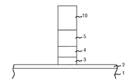
電子デバイス素子の継続的なサイズ縮小は、デバイス性能に問題を提起し、これは新しい材料及び製造技術を用いて対処されなければならない。これらの問題は、高性能CMOSデバイスのゲート構造体の場合に、特に深刻である。一般的なCMOSゲート構造体が、図1に概略的に示される。ゲート構造体100(多くの場合、ゲート・スタックと呼ばれる)が、基板1の表面上に製造され、これは一般に半導体ウェハ(例えば、Si、Ge、SiGe、並びに、埋込絶縁体上の半導体)である。ソース及びドレイン領域22、23が、ウェハの表面付近に形成される。ゲート構造体100には、誘電体層112の上に重なる導電性素子110(一般にポリシリコンであり、PFET及びNFETにおいて、それぞれp+ドープ及びn+ドープされたもの)が含まれる。現在のデバイスでは、ゲート誘電体の酸化物厚さは2nm未満に減少している。同時に線幅が減少されて、ゲート構造体100の横方向領域が今では65nm以下の範囲内である。
The continued size reduction of electronic device elements poses a problem in device performance, which must be addressed using new materials and manufacturing techniques. These problems are particularly acute in the case of gate structures for high performance CMOS devices. A typical CMOS gate structure is schematically illustrated in FIG. A gate structure 100 (often referred to as a gate stack) is fabricated on the surface of the
今日のゲート誘電体厚さにおいては、ゲートが作動し、電荷のない領域がポリシリコン/誘電体のインターフェース(図1のインターフェース112a)に形成されるときに発生するポリシリコン空乏の影響を最小にすることが望ましい。この空乏領域の出現は、ゲートの静電容量を低下させ、従って、電気的厚さが増加されて、デバイス性能が低下する。ポリシリコンの空乏領域を取り除くことができる場合には、漏れ電流の実質的な増加なしで、電気的誘電体厚さを減らすことができる。このことは、ゲート誘電体112の厚さをさらに減らすことなく、改善されたデバイス性能を可能にする。
Today's gate dielectric thickness minimizes the effects of polysilicon depletion that occurs when the gate is activated and an uncharged region is formed at the polysilicon / dielectric interface (
従って、いくつかの利点を得ることができるため、ゲート構造体からポリシリコンを取り除く(又は、少なくともゲート誘電体との接触からポリシリコンを取り除く)ことが望ましい。ポリシリコン空乏の影響をなくすことにより、ゲート誘電体の有効電気的厚さが減る。ポリシリコンとゲート誘電体材料との間の相互作用は回避され、これは次いで、ホウ素浸透に関する問題を回避することができる。このことは、消費電力の少ない迅速なデバイスをもたらすことができる。ポリシリコンを他の材料で置き換えることは、さらに、高kゲート誘電体と互換性があるゲート・スタックの新しい設計を可能にすることができる。 Therefore, it is desirable to remove the polysilicon from the gate structure (or at least remove the polysilicon from contact with the gate dielectric) since several advantages can be obtained. By eliminating the effects of polysilicon depletion, the effective electrical thickness of the gate dielectric is reduced. Interaction between the polysilicon and the gate dielectric material is avoided, which in turn can avoid problems with boron penetration. This can result in a quick device with low power consumption. Replacing polysilicon with other materials can also allow new designs of gate stacks that are compatible with high-k gate dielectrics.
最近では、ポリシリコン・ゲート導体を金属シリサイド・ゲート電極で置き換えることに、大きな関心が寄せられている。一般に、シリサイド化ゲートの形成には、金属層を、ゲート誘電体と接触している、下にあるシリコン層(ポリシリコン又はアモルファス・シリコン)と反応させることを含む。従来のポリシリコン・ゲートの製造と比較すると、相当な数の付加的なプロセス・ステップが必要になる。さらに、一般的なシリサイド・ゲートの製造スキームには、ポリシリコン層の化学的機械研磨(CMP:chemical−mechanical polishing)又はエッチ・バックが必要である。これらのプロセスは、多くの場合、ポリシリコンの厚さにおいて(ウェハ全体に)十分な一様性をもたらすことができない。このことは、次いで、低品質シリサイド化ゲート及び歩留まりの低いデバイスをもたらす。 Recently, there has been great interest in replacing polysilicon gate conductors with metal silicide gate electrodes. In general, the formation of a silicided gate involves reacting the metal layer with an underlying silicon layer (polysilicon or amorphous silicon) in contact with the gate dielectric. Compared to conventional polysilicon gate fabrication, a considerable number of additional process steps are required. Further, typical silicide gate fabrication schemes require chemical-mechanical polishing (CMP) or etch back of the polysilicon layer. These processes often fail to provide sufficient uniformity (over the entire wafer) in polysilicon thickness. This in turn results in low quality silicidated gates and low yield devices.
従って、付加的なステップの数を最小限とし、従来の製造技術に関わる非一様性の問題を回避する金属シリサイド化ゲート構造体の製造プロセスが必要である。 Accordingly, there is a need for a metal silicided gate structure fabrication process that minimizes the number of additional steps and avoids non-uniformity problems associated with conventional fabrication techniques.
本発明は、金属シリサイド化ゲート構造体が自己形成される(すなわち、別個の金属/シリコン反応ステップを必要とせずに形成される)プロセスを提供することによって、上述の必要性に対処する。ポリシリコンのCMP又はエッチ・バックは必要なく、従来のポリシリコン・ゲート・プロセスと比較すると、付加的なステップが1つだけ用いられる。本発明の第1の態様によれば、このことは、ゲート誘電体の上に第1のシリコン材料層(ポリシリコンであってもよいし又はアモルファス・シリコンであってもよい)を形成するステップと、第1のシリコン材料層の上に金属層を形成するステップと、次いで、金属層の上に第2のシリコン材料層を形成するステップと、によって行われる。これらの層が形成された後で、少なくとも1つの高温(>700℃)処理ステップが実施され、このステップは、金属層を第1のシリコン材料層におけるシリコンと反応させることにより、ゲート誘電体の上に第1のシリサイド層を形成するのに有効である。第1のシリサイド層の厚さは、第1の高温処理ステップにおいて、第1のシリコン材料層の少なくとも一部及び第2のシリコン材料層の少なくとも一部が金属層と反応して、第1のシリサイド層を形成するような厚さである。第2のシリコン材料層におけるシリコンから第2のシリサイド層を形成するのに有効な第2の高温処理ステップを実施することができ、第2のシリサイド層は、第1のシリサイド層の上に重なり、それと接触する。高温プロセスの結果として、第1のシリコン材料層におけるシリコンの実質的にすべてが、シリサイド材料で置き換えられる。 The present invention addresses the aforementioned needs by providing a process in which a metal silicided gate structure is self-formed (ie, formed without the need for a separate metal / silicon reaction step). There is no need for CMP or etch back of polysilicon, and only one additional step is used compared to conventional polysilicon gate processes. According to the first aspect of the invention, this comprises the step of forming a first silicon material layer (which may be polysilicon or amorphous silicon) on the gate dielectric. And forming a metal layer on the first silicon material layer and then forming a second silicon material layer on the metal layer. After these layers are formed, at least one high temperature (> 700 ° C.) processing step is performed, which comprises reacting the metal layer with silicon in the first silicon material layer to form the gate dielectric. This is effective for forming the first silicide layer thereon. In the first high temperature processing step, the thickness of the first silicide layer is such that at least a part of the first silicon material layer and at least a part of the second silicon material layer react with the metal layer. The thickness is such that a silicide layer is formed. A second high temperature processing step effective to form a second silicide layer from silicon in the second silicon material layer can be performed, the second silicide layer overlying the first silicide layer. Contact with it. As a result of the high temperature process, substantially all of the silicon in the first silicon material layer is replaced with a silicide material.
本発明の一実施形態においては、第1の高温処理ステップは、FETデバイスのソース及びドレイン部分のアニール・ステップであり、或いは、このステップは、後に続く処理で実施される他の高温アニール・ステップのいずれかとすることができる。第2の高温処理ステップは、FETデバイスのソース及びドレイン部分のシリサイド化プロセスである。金属は、W、Ti、Pt、Ta、Nb、Hf及びMoの1つとすることができる。第1、第2のシリコン材料層のシリコンの実質的にすべてが反応し、シリサイド材料を形成して、完全シリサイド化ゲート構造体が生成される。 In one embodiment of the invention, the first high temperature processing step is an annealing step of the source and drain portions of the FET device, or this step is another high temperature annealing step performed in a subsequent process. It can be either. The second high temperature processing step is a silicidation process of the source and drain portions of the FET device. The metal can be one of W, Ti, Pt, Ta, Nb, Hf and Mo. Substantially all of the silicon in the first and second silicon material layers react to form a silicide material to produce a fully silicided gate structure.
本発明の別の実施形態においては、第1の高温処理ステップの後で実施される第2の高温処理ステップは、第2のシリコン材料層におけるシリコン材料から第2のシリサイド層を形成するのに有効であり、この第2のシリサイド層は、第2のシリコン材料層におけるシリコンの残存部分の上に重なる。 In another embodiment of the present invention, a second high temperature processing step performed after the first high temperature processing step includes forming a second silicide layer from a silicon material in the second silicon material layer. Effectively, this second silicide layer overlies the remaining portion of silicon in the second silicon material layer.
本発明の第2の態様によれば、基板上のゲート誘電体と、ゲート誘電体の上に重なり、それと接触する第1のシリサイド層と、第1のシリサイド層の上に重なる第2のシリサイド層と、を含むFETデバイスのシリサイド化ゲート構造体が提供される。第2のシリサイド層は、FETのソース及びドレイン領域におけるシリサイドと同じ材料である。ゲート構造体は、完全にシリサイド化することができる(すわなち、ゲート誘電体の上に重なる材料は、本質的に、第1及び第2のシリサイド層におけるシリサイドから構成することができる)。或いは、ゲート構造体は、第1のシリサイド層と第2のシリサイド層との間に第3のシリコン層を含むことができる。 According to a second aspect of the present invention, a gate dielectric on the substrate, a first silicide layer overlying and in contact with the gate dielectric, and a second silicide overlying the first silicide layer. And a silicided gate structure of an FET device including the layer. The second silicide layer is the same material as the silicide in the source and drain regions of the FET. The gate structure can be fully silicided (ie, the material overlying the gate dielectric can consist essentially of silicide in the first and second silicide layers). Alternatively, the gate structure can include a third silicon layer between the first silicide layer and the second silicide layer.
以下の説明においては、シリサイド化ゲート構造体の形成開始までは、従来のCMOS製造技術が用いられることが仮定される。図2は、ゲートを形成するのに用いられる堆積ステップの順序を示す。最初に、ゲート誘電体層2が基板1の上に形成される。基板1は、バルク半導体のウェハ(Si、Ge、SiGe及び同様なもの)であってもよいし、又は、絶縁体上の半導体材料(酸化物、窒化物、酸窒化物及び同様なもの)であってもよい。ゲート誘電体2は、酸化物、酸窒化物、高k材料、HfO2及び同様なものとすることができる。薄いシリコン材料層(第1のシリコン材料層)3がゲート誘電体層2の上に堆積され、次いで金属層4がその上に堆積される。本実施形態においては、シリコン材料層3はポリシリコンであるが、この材料はアモルファス・シリコンであってもよい。金属層4は、熱的に安定したシリサイドを有する金属であるように選択され、このシリサイドは高温(>700℃)での反応によって形成され、この必要条件を満たす金属には、W、Ti、Pt、Ta、Nb、Hf及びMoが含まれる。シリコン材料層3及び金属層4の厚さは、シリコン材料層3におけるシリコン材料が、後で実施される高温プロセス中に完全にシリサイド化されることを保証するように選択される。さらに、シリコン材料層3におけるシリコンは、後で形成されるシリサイドが、製造されるデバイスの種類(例えばPFET又はNFET)に適した動作機能を有するように、金属層4の堆積前にドープすることができる。
In the following description, it is assumed that conventional CMOS manufacturing techniques are used until the formation of the silicided gate structure. FIG. 2 shows the sequence of deposition steps used to form the gate. First, a gate
別のシリコン材料層5(第2のシリコン材料層、本実施形態ではポリシリコンであるが、或いはアモルファス・シリコン)が、金属層4の上部に堆積される。本発明の本実施形態においては、従来のゲート製造プロセスと比較すると、1つの追加的な堆積ステップ、すなわち、シリコン材料層3,5が単一層ではなく2つの層として堆積されるステップが実施されることが理解されるであろう。
Another silicon material layer 5 (second silicon material layer, which in this embodiment is polysilicon or amorphous silicon) is deposited on top of the
次いで、基板1はフォトレジスト10を用いてパターン形成され、シリコン材料層3から別のシリコン材料層5までが、ゲート構造体を定めるようにエッチングされる。これらのエッチング・プロセスの結果は、図3に示される。次いで、スペーサ25並びにソース及びドレイン領域40を含むゲート構造体を生成するように、当該技術分野において既知の技術を用いて、さらに別のプロセス・ステップが実施される。この時点で用いられる一般的なプロセスは、ソース及びドレインに対する高温活性化アニールである。このアニール・ステップにおいては、金属層4が下にあるシリコン材料層3と反応して、シリサイド層30(例えば、WSix、TiSix、PtSix、TaSix、NbSix、HfSix、MoSix)を生成する。上述のように、本実施形態においては、シリコン層3及び金属層4の厚さはシリコン材料、層3におけるシリコン材料が完全にシリサイド化される(すなわち、シリコン材料層3がシリサイド層30に置き換えられる)ように選択される。従って、図4に示されるように、シリサイド層30は、ゲート誘電体2に接触しており、別のシリコン材料層5からの未反応シリコン材料がシリサイド層30の上にある。
The
別の形態として、1つより多い高温プロセスが用いられる場合には、第1の高温プロセス(例えば活性化アニール)において、シリコン材料層3におけるすべてのシリコン材料を金属層4における金属と反応させない(シリコン材料層3が完全にシリサイド化されない)ようにすることが可能である。具体的には、このことは、第1の高温プロセスの熱量に限りがある場合に当て嵌まるとすることができる。この場合においては、図5に示されるように、第1の高温プロセス後で、シリコン材料の残存層33がゲート誘電体2の上に重なり、シリサイド層31は、シリサイドの金属リッチ相である。第2の高温プロセス(詳細は以下に論じる)においては、残像層33におけるシリコン材料が反応されて、シリサイド材料(層30と同じ材料)を形成し、シリコン材料層3は、第2の高温プロセス後で完全にシリサイド化される。
Alternatively, if more than one high temperature process is used, all silicon material in the
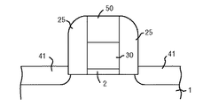
次いで、金属(例えばNi、Co、Ti、Pt及び同様なもの)が、FET構造体の上に堆積されて、その金属が、別のシリコン層5におけるシリコン材料、並びに、ソース/ドレイン領域40と接触するようになる。次いで、(当該技術分野において既知の)さらに別のシリサイド形成プロセスが実施されて、ソース及びドレイン領域40に導電性シリサイド領域41を形成する。この同じプロセスは、ゲート上部におけるシリコンを金属と反応させて、ゲートの上方部分にシリサイド領域50を形成する(さらに、残存層33における残存シリコン材料がある場合には、シリサイドに変換する)。結果として得られる構造体が図6に示される。従って、ソース/ドレイン領域41及びゲート領域50におけるシリサイド材料は同じであり、ゲートの下方部分のシリサイド層30は、ゲート領域50と同じ材料であってもよいし又は異なる材料であってもよい。(さらに、(下方)シリサイド層30と(上方)シリサイド層50との間に、シリサイド材料の混合物をもつ遷移層があってもよい。)従って、ゲート構造体に最初に堆積されたシリコンは、シリサイド材料で置き換えられ、すなわち、ゲート構造体は完全にシリサイド化されたと言える。従来のCMOS製造プロセスと比較すると、完全シリサイド化ゲートは、堆積プロセス・ステップを1つだけ加えることによって生成され、ポリシリコン層のCMP又はエッチング・プロセスは必要としないことが理解される。さらに、ゲート材料のシリサイド化は、後に続く高温プロセスの結果として生じ、ゲートにシリサイド層を形成するために、別個のプロセスを必要とすることはない。
A metal (eg, Ni, Co, Ti, Pt, and the like) is then deposited over the FET structure, and the metal is added to the silicon material in another
本発明の代替的な実施形態においては、別のシリコン材料層5の厚さは、シリサイド30の上に重なるシリコン材料が、ソース/ドレインのシリサイド化プロセス中に、完全にシリサイドに変換されないように選択される。従って、ゲート誘電体2の上には、シリサイド層30、シリコン層55及びシリサイド層50(ソース/ドレイン領域41と同じシリサイド材料)の3つのゲート材料が存在することになる。この構造体は図7に示される。
In an alternative embodiment of the present invention, the thickness of another
上述のように、本発明のゲート製造プロセスは従来のプロセスより単純であり、自己位置合わせシリサイド・ゲート導体の自動形成を可能にする。 As mentioned above, the gate fabrication process of the present invention is simpler than conventional processes and allows for the automatic formation of self-aligned silicide gate conductors.
本発明は、特定の好ましい実施形態と併せて説明されたが、多くの代替的手法、修正及び変形を、本発明の範囲及び精神から逸脱することなく行うことができることが当業者には明らかであろう。従って、本発明は、本発明の範囲及び精神並びに添付の特許請求の範囲に含まれる、こうしたすべての代替的手法、修正及び変形を包含することが意図される。 While the invention has been described in conjunction with certain preferred embodiments, it will be apparent to those skilled in the art that many alternative approaches, modifications, and variations can be made without departing from the scope and spirit of the invention. I will. Accordingly, the present invention is intended to embrace all such alternatives, modifications and variations that fall within the scope and spirit of the present invention and the appended claims.
本発明は、半導体製造分野において実用性を有し、通信、電子技術、医療機器、航空宇宙用途及び同様なもの含むすべての種類の用途における、すべての大規模集積回路チップに適用できるという利点がある。 The present invention has the advantage that it has utility in the field of semiconductor manufacturing and can be applied to all large scale integrated circuit chips in all kinds of applications including communications, electronics, medical equipment, aerospace applications and the like. is there.
Claims (20)
前記ゲート誘電体(2)の上に第1のシリコン材料層(3)を形成するステップと、
前記第1のシリコン材料層(3)の上に金属層(4)を形成するステップと、
前記金属層(4)の上に第2のシリコン材料層(5)を形成するステップと、
前記形成ステップの後で前記高温プロセスを実施するステップと、
を含み、前記高温プロセスが、前記金属を前記第1のシリコン材料層(3)における前記シリコン材料と反応させることにより、前記ゲート誘電体(2)に接触する第1のシリサイド層(30)を形成するのに有効であり、前記第1のシリコン材料層(3)における前記シリコン材料が、前記第1のシリサイド層(30)におけるシリサイド材料で置き換えられる、方法。 A method for forming a silicided gate structure (100) having a gate dielectric (2) on a substrate (1) in a fabrication process of an FET device comprising at least one high temperature process comprising:
Forming a first silicon material layer (3) on the gate dielectric (2);
Forming a metal layer (4) on the first silicon material layer (3);
Forming a second silicon material layer (5) on the metal layer (4);
Performing the high temperature process after the forming step;
And the high temperature process comprises reacting the metal with the silicon material in the first silicon material layer (3) to thereby form a first silicide layer (30) in contact with the gate dielectric (2). A method that is effective to form and wherein the silicon material in the first silicon material layer (3) is replaced with a silicide material in the first silicide layer (30).
前記第2の高温プロセスが、前記第2のシリコン材料層(5)における前記シリコン材料から第2のシリサイド層(50)を形成するのに有効であり、前記第2のシリサイド層(50)が前記第1のシリサイド層(30)の上に重なり、それと接触している、請求項1に記載の方法。 The high temperature process includes a first high temperature process and a second high temperature process, wherein the second high temperature process is performed after the first high temperature processing step;
The second high temperature process is effective to form a second silicide layer (50) from the silicon material in the second silicon material layer (5), wherein the second silicide layer (50) The method of any preceding claim, wherein the method overlies and is in contact with the first silicide layer (30).
前記第2の高温プロセスが、前記第2のシリコン材料層(5)における前記シリコン材料から第2のシリサイド層(50)を形成するのに有効であり、前記第2のシリサイド層(50)が前記第2のシリコン材料層(5)の残存部分(55)の上に重なる、請求項1に記載の方法。 The high temperature process includes a first high temperature process and a second high temperature process, wherein the second high temperature process is performed after the first high temperature processing step;
The second high temperature process is effective to form a second silicide layer (50) from the silicon material in the second silicon material layer (5), wherein the second silicide layer (50) The method according to claim 1, wherein the second silicon material layer (5) overlies the remaining portion (55).
前記ゲート誘電体(2)の上に第1のシリコン材料層(3)を形成するステップと、
前記第1のシリコン材料層(3)の上に金属層(4)を形成するステップと、
前記金属層(4)の上に第2のシリコン材料層(5)を形成するステップと、
前記金属層(4)を前記第1のシリコン材料層(3)における前記シリコン材料と反応させることにより、第1のシリサイド層(30)を前記ゲート誘電体(2)の上に形成するように第1の高温プロセスを実施するステップと、
前記第1のシリサイド層(30)の上に第2のシリサイド層(50)を形成するように第2の高温プロセス・ステップを実施するステップと、
を含み、前記第1のシリコン材料の層(3)及び前記第2のシリコン材料の層(5)の実質的にすべてが、前記第1及び第2の高温プロセスの結果として反応して、シリサイド化ゲート構造体(100)を形成する、方法。 A method for forming a silicided gate structure (100) having a gate dielectric (2) on a substrate (1) in a FET device manufacturing process comprising:
Forming a first silicon material layer (3) on the gate dielectric (2);
Forming a metal layer (4) on the first silicon material layer (3);
Forming a second silicon material layer (5) on the metal layer (4);
A first silicide layer (30) is formed on the gate dielectric (2) by reacting the metal layer (4) with the silicon material in the first silicon material layer (3). Performing a first high temperature process;
Performing a second high temperature process step to form a second silicide layer (50) over the first silicide layer (30);
And substantially all of the first silicon material layer (3) and the second silicon material layer (5) are reacted as a result of the first and second high temperature processes to form a silicide. Forming a gate structure (100).
前記第2の高温プロセスの結果として、前記シリコン材料が反応して、前記ゲート誘電体(2)と接触するシリサイド層(30)を形成する、請求項13に記載の方法。 As a result of the first high temperature process, a silicide layer (31) overlies the remaining layer (33) of silicon material in contact with the gate dielectric (2);
The method of claim 13, wherein as a result of the second high temperature process, the silicon material reacts to form a silicide layer (30) in contact with the gate dielectric (2).
基板(1)の上のゲート誘電体(2)と、
前記ゲート誘電体(2)の上に重なり、それと接触する第1のシリサイド層(30)と、
前記第1のシリサイド層(30)の上に重なる第2のシリサイド層(50)と、
を含み、
前記第2の層(50)が前記FETデバイスのソース及びドレイン領域(41)におけるシリサイドと同じ材料であり、
前記第1のシリサイドが金属シリサイドであり、前記金属シリサイドの金属がW、Ti、Pt、Ta、Nb、Hf及びMoから構成される群から選択される、
FETデバイスのゲート構造体(100)。 A gate structure of a FET device, comprising:
A gate dielectric (2) on the substrate (1);
A first silicide layer (30) overlying and in contact with said gate dielectric (2);
A second silicide layer (50) overlying the first silicide layer (30);
Including
The second layer (50) is the same material as the silicide in the source and drain regions (41) of the FET device;
The first silicide is a metal silicide, and the metal of the metal silicide is selected from the group consisting of W, Ti, Pt, Ta, Nb, Hf, and Mo;
FET device gate structure (100).
Applications Claiming Priority (2)
| Application Number | Priority Date | Filing Date | Title |
|---|---|---|---|
| US10/905,629 US7105440B2 (en) | 2005-01-13 | 2005-01-13 | Self-forming metal silicide gate for CMOS devices |
| PCT/US2006/000838 WO2006076373A1 (en) | 2005-01-13 | 2006-01-10 | Self-forming metal silicide gate for cmos devices |
Publications (2)
| Publication Number | Publication Date |
|---|---|
| JP2008527743A true JP2008527743A (en) | 2008-07-24 |
| JP2008527743A5 JP2008527743A5 (en) | 2008-12-04 |
Family
ID=36653783
Family Applications (1)
| Application Number | Title | Priority Date | Filing Date |
|---|---|---|---|
| JP2007551329A Pending JP2008527743A (en) | 2005-01-13 | 2006-01-10 | Self-formed metal silicidation gate for CMOS devices |
Country Status (7)
| Country | Link |
|---|---|
| US (1) | US7105440B2 (en) |
| EP (1) | EP1856725A4 (en) |
| JP (1) | JP2008527743A (en) |
| KR (1) | KR20070095933A (en) |
| CN (1) | CN100505187C (en) |
| TW (1) | TW200636920A (en) |
| WO (1) | WO2006076373A1 (en) |
Cited By (1)
| Publication number | Priority date | Publication date | Assignee | Title |
|---|---|---|---|---|
| JP2007080955A (en) * | 2005-09-12 | 2007-03-29 | Nec Corp | Semiconductor device and manufacturing method thereof |
Families Citing this family (6)
| Publication number | Priority date | Publication date | Assignee | Title |
|---|---|---|---|---|
| US7687396B2 (en) * | 2006-12-29 | 2010-03-30 | Texas Instruments Incorporated | Method of forming silicided gates using buried metal layers |
| KR100852212B1 (en) | 2007-06-12 | 2008-08-13 | 삼성전자주식회사 | Semiconductor device and method of manufacturing the semiconductor device |
| US7615831B2 (en) * | 2007-10-26 | 2009-11-10 | International Business Machines Corporation | Structure and method for fabricating self-aligned metal contacts |
| US7964923B2 (en) | 2008-01-07 | 2011-06-21 | International Business Machines Corporation | Structure and method of creating entirely self-aligned metallic contacts |
| US8765603B2 (en) * | 2011-08-01 | 2014-07-01 | Taiwan Semiconductor Manufacturing Company, Ltd. | Method of forming a buffer layer |
| US9165826B2 (en) | 2011-08-01 | 2015-10-20 | Taiwan Semiconductor Manufacturing Company, Ltd. | Method of forming a semiconductor device comprising titanium silicon oxynitride |
Citations (4)
| Publication number | Priority date | Publication date | Assignee | Title |
|---|---|---|---|---|
| JPH06244136A (en) * | 1992-12-25 | 1994-09-02 | Hitachi Ltd | Semiconductor device and its manufacture |
| JPH1117182A (en) * | 1997-06-26 | 1999-01-22 | Sony Corp | Semiconductor device and manufacture thereof |
| JPH11135789A (en) * | 1997-10-31 | 1999-05-21 | Nippon Steel Corp | Semiconductor device and its manufacture |
| JP2000252462A (en) * | 1999-03-01 | 2000-09-14 | Toshiba Corp | Mis semiconductor device and manufacture thereof |
Family Cites Families (7)
| Publication number | Priority date | Publication date | Assignee | Title |
|---|---|---|---|---|
| KR950003233B1 (en) * | 1992-05-30 | 1995-04-06 | 삼성전자 주식회사 | Semiconductor device having double silicide structure and fabricating method thereof |
| US5444302A (en) * | 1992-12-25 | 1995-08-22 | Hitachi, Ltd. | Semiconductor device including multi-layer conductive thin film of polycrystalline material |
| CN1222754A (en) * | 1997-12-19 | 1999-07-14 | 西门子公司 | Method and apparatus for performing chemical vapor deposition on silicide films |
| US6562718B1 (en) * | 2000-12-06 | 2003-05-13 | Advanced Micro Devices, Inc. | Process for forming fully silicided gates |
| US6555453B1 (en) * | 2001-01-31 | 2003-04-29 | Advanced Micro Devices, Inc. | Fully nickel silicided metal gate with shallow junction formed |
| US6878623B2 (en) * | 2001-02-01 | 2005-04-12 | Chartered Semiconductor Manufacturing Ltd. | Technique to achieve thick silicide film for ultra-shallow junctions |
| US7029966B2 (en) * | 2003-09-18 | 2006-04-18 | International Business Machines Corporation | Process options of forming silicided metal gates for advanced CMOS devices |
-
2005
- 2005-01-13 US US10/905,629 patent/US7105440B2/en not_active Expired - Fee Related
-
2006
- 2006-01-04 TW TW095100297A patent/TW200636920A/en unknown
- 2006-01-10 EP EP06717971A patent/EP1856725A4/en active Pending
- 2006-01-10 KR KR1020077015594A patent/KR20070095933A/en not_active Application Discontinuation
- 2006-01-10 WO PCT/US2006/000838 patent/WO2006076373A1/en active Application Filing
- 2006-01-10 CN CNB2006800014309A patent/CN100505187C/en not_active Expired - Fee Related
- 2006-01-10 JP JP2007551329A patent/JP2008527743A/en active Pending
Patent Citations (4)
| Publication number | Priority date | Publication date | Assignee | Title |
|---|---|---|---|---|
| JPH06244136A (en) * | 1992-12-25 | 1994-09-02 | Hitachi Ltd | Semiconductor device and its manufacture |
| JPH1117182A (en) * | 1997-06-26 | 1999-01-22 | Sony Corp | Semiconductor device and manufacture thereof |
| JPH11135789A (en) * | 1997-10-31 | 1999-05-21 | Nippon Steel Corp | Semiconductor device and its manufacture |
| JP2000252462A (en) * | 1999-03-01 | 2000-09-14 | Toshiba Corp | Mis semiconductor device and manufacture thereof |
Cited By (1)
| Publication number | Priority date | Publication date | Assignee | Title |
|---|---|---|---|---|
| JP2007080955A (en) * | 2005-09-12 | 2007-03-29 | Nec Corp | Semiconductor device and manufacturing method thereof |
Also Published As
| Publication number | Publication date |
|---|---|
| EP1856725A4 (en) | 2009-01-14 |
| CN100505187C (en) | 2009-06-24 |
| CN101080811A (en) | 2007-11-28 |
| WO2006076373A1 (en) | 2006-07-20 |
| KR20070095933A (en) | 2007-10-01 |
| US7105440B2 (en) | 2006-09-12 |
| EP1856725A1 (en) | 2007-11-21 |
| TW200636920A (en) | 2006-10-16 |
| US20060154413A1 (en) | 2006-07-13 |
Similar Documents
| Publication | Publication Date | Title |
|---|---|---|
| KR101027107B1 (en) | Metal gate mosfet by full semiconductor metal alloy conversion | |
| US7112483B2 (en) | Method for forming a device having multiple silicide types | |
| US7504336B2 (en) | Methods for forming CMOS devices with intrinsically stressed metal silicide layers | |
| US7381619B2 (en) | Dual work-function metal gates | |
| US7067379B2 (en) | Silicide gate transistors and method of manufacture | |
| US7271045B2 (en) | Etch stop and hard mask film property matching to enable improved replacement metal gate process | |
| JP5305907B2 (en) | High performance MOSFET including stressed gate metal silicide layer and method of manufacturing the same | |
| US6905922B2 (en) | Dual fully-silicided gate MOSFETs | |
| US7741220B2 (en) | Semiconductor device and manufacturing method thereof | |
| JP2003060076A (en) | Semiconductor device and manufacturing method therefor | |
| US7432566B2 (en) | Method and system for forming dual work function gate electrodes in a semiconductor device | |
| JP2003037264A (en) | Semiconductor device and manufacturing method therefor | |
| US20070145488A1 (en) | Semiconductor device and manufacturing method thereof | |
| US7105440B2 (en) | Self-forming metal silicide gate for CMOS devices | |
| US20070173025A1 (en) | Semiconductor device and method for fabricating the same | |
| JP2008288364A (en) | Semiconductor device, and manufacturing method of semiconductor device | |
| US20090057786A1 (en) | Semiconductor device and method of manufacturing semiconductor device | |
| TWI446447B (en) | Method for forming a thin film resistor | |
| JP2007141903A (en) | Semiconductor device and its manufacturing method | |
| KR20090109303A (en) | Metal oxide semiconductor field effect transistor and method for fabricating the same | |
| JP2010161400A (en) | Semiconductor device and production method of the same | |
| JP2003100770A (en) | Semiconductor device and its manufacturing method |
Legal Events
| Date | Code | Title | Description |
|---|---|---|---|
| A521 | Written amendment |
Free format text: JAPANESE INTERMEDIATE CODE: A523 Effective date: 20081020 |
|
| A621 | Written request for application examination |
Free format text: JAPANESE INTERMEDIATE CODE: A621 Effective date: 20081020 |
|
| A131 | Notification of reasons for refusal |
Free format text: JAPANESE INTERMEDIATE CODE: A131 Effective date: 20120321 |
|
| A977 | Report on retrieval |
Free format text: JAPANESE INTERMEDIATE CODE: A971007 Effective date: 20120322 |
|
| A02 | Decision of refusal |
Free format text: JAPANESE INTERMEDIATE CODE: A02 Effective date: 20120821 |