JP2008510320A - Gradient semiconductor layer - Google Patents
Gradient semiconductor layer Download PDFInfo
- Publication number
- JP2008510320A JP2008510320A JP2007527945A JP2007527945A JP2008510320A JP 2008510320 A JP2008510320 A JP 2008510320A JP 2007527945 A JP2007527945 A JP 2007527945A JP 2007527945 A JP2007527945 A JP 2007527945A JP 2008510320 A JP2008510320 A JP 2008510320A
- Authority
- JP
- Japan
- Prior art keywords
- semiconductor layer
- germanium
- layer
- concentration
- silicon
- Prior art date
- Legal status (The legal status is an assumption and is not a legal conclusion. Google has not performed a legal analysis and makes no representation as to the accuracy of the status listed.)
- Pending
Links
- 239000004065 semiconductor Substances 0.000 title claims abstract description 97
- 238000000034 method Methods 0.000 claims abstract description 90
- GNPVGFCGXDBREM-UHFFFAOYSA-N germanium atom Chemical compound [Ge] GNPVGFCGXDBREM-UHFFFAOYSA-N 0.000 claims abstract description 67
- 229910052732 germanium Inorganic materials 0.000 claims abstract description 66
- 230000008569 process Effects 0.000 claims abstract description 48
- XUIMIQQOPSSXEZ-UHFFFAOYSA-N Silicon Chemical compound [Si] XUIMIQQOPSSXEZ-UHFFFAOYSA-N 0.000 claims abstract description 39
- 229910052710 silicon Inorganic materials 0.000 claims abstract description 39
- 239000010703 silicon Substances 0.000 claims abstract description 39
- 238000009833 condensation Methods 0.000 claims abstract description 34
- 230000005494 condensation Effects 0.000 claims abstract description 34
- 239000000463 material Substances 0.000 claims description 15
- 239000012212 insulator Substances 0.000 claims description 13
- 238000005229 chemical vapour deposition Methods 0.000 claims description 6
- 230000003647 oxidation Effects 0.000 claims description 5
- 238000007254 oxidation reaction Methods 0.000 claims description 5
- VYPSYNLAJGMNEJ-UHFFFAOYSA-N Silicium dioxide Chemical compound O=[Si]=O VYPSYNLAJGMNEJ-UHFFFAOYSA-N 0.000 claims description 3
- 229910052814 silicon oxide Inorganic materials 0.000 claims description 2
- 238000009827 uniform distribution Methods 0.000 claims 3
- 238000000407 epitaxy Methods 0.000 claims 1
- 229910000577 Silicon-germanium Inorganic materials 0.000 abstract description 16
- LEVVHYCKPQWKOP-UHFFFAOYSA-N [Si].[Ge] Chemical compound [Si].[Ge] LEVVHYCKPQWKOP-UHFFFAOYSA-N 0.000 abstract description 16
- 238000009825 accumulation Methods 0.000 abstract 1
- 235000012431 wafers Nutrition 0.000 description 25
- 239000007789 gas Substances 0.000 description 11
- 238000004519 manufacturing process Methods 0.000 description 6
- 230000008901 benefit Effects 0.000 description 3
- 238000000151 deposition Methods 0.000 description 3
- 238000009792 diffusion process Methods 0.000 description 3
- 239000000758 substrate Substances 0.000 description 3
- 230000015572 biosynthetic process Effects 0.000 description 2
- 230000008859 change Effects 0.000 description 2
- 230000008018 melting Effects 0.000 description 2
- 238000002844 melting Methods 0.000 description 2
- 230000004048 modification Effects 0.000 description 2
- 238000012986 modification Methods 0.000 description 2
- OKTJSMMVPCPJKN-UHFFFAOYSA-N Carbon Chemical compound [C] OKTJSMMVPCPJKN-UHFFFAOYSA-N 0.000 description 1
- KGVOWMMMRLCVHS-UHFFFAOYSA-N Cl[SiH2]Cl.Cl.Cl Chemical compound Cl[SiH2]Cl.Cl.Cl KGVOWMMMRLCVHS-UHFFFAOYSA-N 0.000 description 1
- 229910004298 SiO 2 Inorganic materials 0.000 description 1
- BLRPTPMANUNPDV-UHFFFAOYSA-N Silane Chemical compound [SiH4] BLRPTPMANUNPDV-UHFFFAOYSA-N 0.000 description 1
- 229910000681 Silicon-tin Inorganic materials 0.000 description 1
- KCFIHQSTJSCCBR-UHFFFAOYSA-N [C].[Ge] Chemical compound [C].[Ge] KCFIHQSTJSCCBR-UHFFFAOYSA-N 0.000 description 1
- AXQKVSDUCKWEKE-UHFFFAOYSA-N [C].[Ge].[Si] Chemical compound [C].[Ge].[Si] AXQKVSDUCKWEKE-UHFFFAOYSA-N 0.000 description 1
- 230000009286 beneficial effect Effects 0.000 description 1
- 229910052799 carbon Inorganic materials 0.000 description 1
- 230000007423 decrease Effects 0.000 description 1
- 230000008021 deposition Effects 0.000 description 1
- 238000009826 distribution Methods 0.000 description 1
- 239000002019 doping agent Substances 0.000 description 1
- 229910000078 germane Inorganic materials 0.000 description 1
- LQJIDIOGYJAQMF-UHFFFAOYSA-N lambda2-silanylidenetin Chemical compound [Si].[Sn] LQJIDIOGYJAQMF-UHFFFAOYSA-N 0.000 description 1
- 230000007257 malfunction Effects 0.000 description 1
- 230000004899 motility Effects 0.000 description 1
- 239000010453 quartz Substances 0.000 description 1
- 229910052594 sapphire Inorganic materials 0.000 description 1
- 239000010980 sapphire Substances 0.000 description 1
- 229910000077 silane Inorganic materials 0.000 description 1
- 125000006850 spacer group Chemical group 0.000 description 1
- IEXRMSFAVATTJX-UHFFFAOYSA-N tetrachlorogermane Chemical compound Cl[Ge](Cl)(Cl)Cl IEXRMSFAVATTJX-UHFFFAOYSA-N 0.000 description 1
- 238000001039 wet etching Methods 0.000 description 1
Images


Classifications
-
- H—ELECTRICITY
- H01—ELECTRIC ELEMENTS
- H01L—SEMICONDUCTOR DEVICES NOT COVERED BY CLASS H10
- H01L21/00—Processes or apparatus adapted for the manufacture or treatment of semiconductor or solid state devices or of parts thereof
- H01L21/02—Manufacture or treatment of semiconductor devices or of parts thereof
- H01L21/04—Manufacture or treatment of semiconductor devices or of parts thereof the devices having at least one potential-jump barrier or surface barrier, e.g. PN junction, depletion layer or carrier concentration layer
- H01L21/18—Manufacture or treatment of semiconductor devices or of parts thereof the devices having at least one potential-jump barrier or surface barrier, e.g. PN junction, depletion layer or carrier concentration layer the devices having semiconductor bodies comprising elements of Group IV of the Periodic System or AIIIBV compounds with or without impurities, e.g. doping materials
- H01L21/20—Deposition of semiconductor materials on a substrate, e.g. epitaxial growth solid phase epitaxy
-
- H—ELECTRICITY
- H01—ELECTRIC ELEMENTS
- H01L—SEMICONDUCTOR DEVICES NOT COVERED BY CLASS H10
- H01L29/00—Semiconductor devices adapted for rectifying, amplifying, oscillating or switching, or capacitors or resistors with at least one potential-jump barrier or surface barrier, e.g. PN junction depletion layer or carrier concentration layer; Details of semiconductor bodies or of electrodes thereof ; Multistep manufacturing processes therefor
- H01L29/66—Types of semiconductor device ; Multistep manufacturing processes therefor
- H01L29/68—Types of semiconductor device ; Multistep manufacturing processes therefor controllable by only the electric current supplied, or only the electric potential applied, to an electrode which does not carry the current to be rectified, amplified or switched
- H01L29/76—Unipolar devices, e.g. field effect transistors
- H01L29/772—Field effect transistors
- H01L29/78—Field effect transistors with field effect produced by an insulated gate
- H01L29/786—Thin film transistors, i.e. transistors with a channel being at least partly a thin film
- H01L29/78684—Thin film transistors, i.e. transistors with a channel being at least partly a thin film having a semiconductor body comprising semiconductor materials of Group IV not being silicon, or alloys including an element of the group IV, e.g. Ge, SiN alloys, SiC alloys
- H01L29/78687—Thin film transistors, i.e. transistors with a channel being at least partly a thin film having a semiconductor body comprising semiconductor materials of Group IV not being silicon, or alloys including an element of the group IV, e.g. Ge, SiN alloys, SiC alloys with a multilayer structure or superlattice structure
-
- H—ELECTRICITY
- H01—ELECTRIC ELEMENTS
- H01L—SEMICONDUCTOR DEVICES NOT COVERED BY CLASS H10
- H01L29/00—Semiconductor devices adapted for rectifying, amplifying, oscillating or switching, or capacitors or resistors with at least one potential-jump barrier or surface barrier, e.g. PN junction depletion layer or carrier concentration layer; Details of semiconductor bodies or of electrodes thereof ; Multistep manufacturing processes therefor
- H01L29/02—Semiconductor bodies ; Multistep manufacturing processes therefor
- H01L29/06—Semiconductor bodies ; Multistep manufacturing processes therefor characterised by their shape; characterised by the shapes, relative sizes, or dispositions of the semiconductor regions ; characterised by the concentration or distribution of impurities within semiconductor regions
- H01L29/10—Semiconductor bodies ; Multistep manufacturing processes therefor characterised by their shape; characterised by the shapes, relative sizes, or dispositions of the semiconductor regions ; characterised by the concentration or distribution of impurities within semiconductor regions with semiconductor regions connected to an electrode not carrying current to be rectified, amplified or switched and such electrode being part of a semiconductor device which comprises three or more electrodes
- H01L29/1025—Channel region of field-effect devices
- H01L29/1029—Channel region of field-effect devices of field-effect transistors
- H01L29/1033—Channel region of field-effect devices of field-effect transistors with insulated gate, e.g. characterised by the length, the width, the geometric contour or the doping structure
- H01L29/1054—Channel region of field-effect devices of field-effect transistors with insulated gate, e.g. characterised by the length, the width, the geometric contour or the doping structure with a variation of the composition, e.g. channel with strained layer for increasing the mobility
-
- H—ELECTRICITY
- H01—ELECTRIC ELEMENTS
- H01L—SEMICONDUCTOR DEVICES NOT COVERED BY CLASS H10
- H01L29/00—Semiconductor devices adapted for rectifying, amplifying, oscillating or switching, or capacitors or resistors with at least one potential-jump barrier or surface barrier, e.g. PN junction depletion layer or carrier concentration layer; Details of semiconductor bodies or of electrodes thereof ; Multistep manufacturing processes therefor
- H01L29/66—Types of semiconductor device ; Multistep manufacturing processes therefor
- H01L29/66007—Multistep manufacturing processes
- H01L29/66075—Multistep manufacturing processes of devices having semiconductor bodies comprising group 14 or group 13/15 materials
- H01L29/66227—Multistep manufacturing processes of devices having semiconductor bodies comprising group 14 or group 13/15 materials the devices being controllable only by the electric current supplied or the electric potential applied, to an electrode which does not carry the current to be rectified, amplified or switched, e.g. three-terminal devices
- H01L29/66409—Unipolar field-effect transistors
- H01L29/66477—Unipolar field-effect transistors with an insulated gate, i.e. MISFET
- H01L29/66568—Lateral single gate silicon transistors
- H01L29/66575—Lateral single gate silicon transistors where the source and drain or source and drain extensions are self-aligned to the sides of the gate
- H01L29/6659—Lateral single gate silicon transistors where the source and drain or source and drain extensions are self-aligned to the sides of the gate with both lightly doped source and drain extensions and source and drain self-aligned to the sides of the gate, e.g. lightly doped drain [LDD] MOSFET, double diffused drain [DDD] MOSFET
-
- H—ELECTRICITY
- H01—ELECTRIC ELEMENTS
- H01L—SEMICONDUCTOR DEVICES NOT COVERED BY CLASS H10
- H01L29/00—Semiconductor devices adapted for rectifying, amplifying, oscillating or switching, or capacitors or resistors with at least one potential-jump barrier or surface barrier, e.g. PN junction depletion layer or carrier concentration layer; Details of semiconductor bodies or of electrodes thereof ; Multistep manufacturing processes therefor
- H01L29/66—Types of semiconductor device ; Multistep manufacturing processes therefor
- H01L29/66007—Multistep manufacturing processes
- H01L29/66075—Multistep manufacturing processes of devices having semiconductor bodies comprising group 14 or group 13/15 materials
- H01L29/66227—Multistep manufacturing processes of devices having semiconductor bodies comprising group 14 or group 13/15 materials the devices being controllable only by the electric current supplied or the electric potential applied, to an electrode which does not carry the current to be rectified, amplified or switched, e.g. three-terminal devices
- H01L29/66409—Unipolar field-effect transistors
- H01L29/66477—Unipolar field-effect transistors with an insulated gate, i.e. MISFET
- H01L29/66742—Thin film unipolar transistors
Landscapes
- Engineering & Computer Science (AREA)
- Microelectronics & Electronic Packaging (AREA)
- Power Engineering (AREA)
- Physics & Mathematics (AREA)
- Condensed Matter Physics & Semiconductors (AREA)
- General Physics & Mathematics (AREA)
- Computer Hardware Design (AREA)
- Ceramic Engineering (AREA)
- Manufacturing & Machinery (AREA)
- Recrystallisation Techniques (AREA)
- Thin Film Transistor (AREA)
Abstract
半導体装置を形成するプロセス。プロセスは、ストレインドシリコン層(305)を形成するためにテンプレート層(207)を形成することを含む。1例では、下部ではゲルマニウムの濃度がより高く、上部ではゲルマニウムの濃度がより低い、勾配シリコンゲルマニウム層(107)が形成される。凝縮プロセスを受けると、層の上部のゲルマニウムは、シリコンゲルマニウム層の残りの部分に拡散する。シリコンゲルマニウム層は下部でゲルマニウムの濃度がより高いため、シリコンゲルマニウム層の残りの部分の上部では凝縮後のゲルマニウムの集積が低減され得る。A process for forming a semiconductor device. The process includes forming a template layer (207) to form a strained silicon layer (305). In one example, a gradient silicon germanium layer (107) is formed with a higher germanium concentration at the bottom and a lower germanium concentration at the top. Upon undergoing the condensation process, the germanium on top of the layer diffuses into the rest of the silicon germanium layer. Since the silicon germanium layer has a higher germanium concentration in the lower part, the accumulation of germanium after condensation can be reduced in the upper part of the remaining part of the silicon germanium layer.
Description
本発明は、一般に半導体装置に関し、詳細にはストレインドチャネル領域を備えた半導体装置の形成に関する。 The present invention generally relates to semiconductor devices, and more particularly to the formation of semiconductor devices with strained channel regions.
電子と正孔の運動性は、特にセミコンダクター・オン・インシュレータ構成(SOI)を有するウエハから構築された装置に関しては、チャネル領域への(例えば2軸の引張歪みによる)ストレインドシリコンの利用により増強され得る。ストレインドシリコン層は、テンプレート層(例えばシリコンゲルマニウム)にシリコン層を堆積させることにより形成され得る。いくつかのプロセスでは、シリコンの堆積前にシリコンゲルマニウムテンプレート層を弛緩するために、テンプレート層に対して凝縮プロセスが行なわれる。そのような凝縮プロセスの1例は、シリコンゲルマニウムテンプレート層の酸化を含む。そのようなプロセスにより、テンプレート層の上にはSiO2の層が成長すると共に、テンプレート層の消費された部分のゲルマニウムがシリコンゲルマニウム層の残りの部分へと下方に拡散し、残りの部分を濃縮する。続いて、ストレインドシリコンを堆積させる前に、その酸化物はエッチング除去される。 Electron and hole motility is enhanced by the use of strained silicon (eg, due to biaxial tensile strain) in the channel region, especially for devices constructed from wafers with a semiconductor-on-insulator configuration (SOI) Can be done. The strained silicon layer can be formed by depositing a silicon layer on a template layer (eg, silicon germanium). In some processes, a condensation process is performed on the template layer to relax the silicon germanium template layer prior to silicon deposition. One example of such a condensation process involves the oxidation of a silicon germanium template layer. With such a process, a layer of SiO 2 is grown on the template layer, and the consumed portion of germanium diffuses downward into the remaining portion of the silicon germanium layer, concentrating the remaining portion. To do. Subsequently, the oxide is etched away before the strained silicon is deposited.
そのような方法で生じ得る1つの問題は、シリコンゲルマニウム層の残りの部分にゲルマニウムが十分に拡散しない恐れがあるということである。従って、残りの層の上部におけるゲルマニウムの濃度がシリコンゲルマニウム層の下部のゲルマニウム濃度に対して相対的に高い場合がある。テンプレート層中のゲルマニウム濃度のこのような差は転位を引き起こし、これは転位領域に形成された半導体装置の機能不全につながり得る。 One problem that can arise with such a method is that germanium may not diffuse sufficiently into the rest of the silicon germanium layer. Therefore, the germanium concentration in the upper part of the remaining layer may be relatively higher than the germanium concentration in the lower part of the silicon germanium layer. Such a difference in the germanium concentration in the template layer causes dislocation, which can lead to malfunction of the semiconductor device formed in the dislocation region.
半導体装置製造の改良されたプロセスが必要とされている。 There is a need for improved processes for semiconductor device manufacturing.
添付図面を参照すれば、本発明は一層よく理解され、また、本発明の多くの目的、特徴、および利点が当業者には明らかになるであろう。
特段の注意がない限り、異なる図面中の同じ参照符号の使用は同一の部材を示す。図は必ずしも正しい縮尺で描かれているわけではない。
The present invention is better understood and the many objects, features and advantages of the present invention will become apparent to those skilled in the art with reference to the accompanying drawings.
Unless otherwise noted, the use of the same reference symbols in different drawings indicates the same component. The figures are not necessarily drawn to scale.
以下に、本発明を実施するための態様の詳細な説明を述べる。この記述は本発明を例証するものであって、限定とみなされるべきではない。
ゲルマニウムを勾配濃度にしたテンプレート層材料の層を提供することにより、凝縮プロセスが該層に行なわれた後、より勾配が一様なゲルマニウムが与えられることが見出された。
Hereinafter, a detailed description of embodiments for carrying out the present invention will be described. This description is illustrative of the invention and is not to be considered as limiting.
It has been found that providing a layer of germanium-graded template layer material provides a more uniform germanium after the condensation process has been performed on the layer.
図1は、半導体装置の製造中のある段階にあるウエハ101の部分断面図である。示された実施形態では、ウエハ101は、半導体基板103と、基板103上に配置された絶縁層105(例えば酸化物)とを備えている。絶縁層105の上にはシリコン層106(例えば100オングストローム)が配置される。1実施形態では、層106、層105および基板103は、SEVIOXプロセスにより、または別のウエハの酸化物層上に1つのシリコンウエハを接合することにより、形成される。示された実施形態では、ウエハ101は絶縁体の上に半導体がある(セミコンダクター・オン・インシュレータ,SOI)の構成を有している。別の実施形態では、ウエハ101は別のタイプのSOI構成(例えばシリコン・オン・サファイアまたはシリコン・オン・クオーツ)を有してもよい。
FIG. 1 is a partial cross-sectional view of a
示された実施形態では、シリコン層106の上にシリコンゲルマニウム層107が形成される。示された実施形態では、層107のゲルマニウム濃度は、層107の下部の高濃度から層107の上部のより低い濃度まで勾配をつけられている。
In the illustrated embodiment, a
1実施形態では、層107は、化学蒸着(CVD)プロセスによりエピタキシ成長させられる。そのようなプロセスの1つの例では、ゲルマニウム含有ガス(例えばゲルマンまたは四塩化ゲルマニウム)およびシリコン含有ガス(例えばシランまたは二塩化ジクロロシラン)が、ゲルマニウムガス対シリコン含有ガスの第1の比で、層106の上にわたって流される。層107のより高い部分が形成されるにつれて、ゲルマニウムガスとシリコン含有ガスの比は小さくされ、それらの部分のゲルマニウム濃度は低減される。
In one embodiment,
1例において、ゲルマニウムの濃度は層107の底部では50%であり、層107の上部では10%まで徐々に減少される。しかしながら、他の実施形態は他のゲルマニウム勾配分布を有していてもよい。別の実施形態では、層107の底部のゲルマニウムの濃度が100%ゲルマニウムから10%ゲルマニウムまでの範囲であり、層107の上部のゲルマニウム濃度は0−20%の範囲であり得る。しかしながら、別の実施形態では、層107は上部と底部の両方で異なるゲルマニウム濃度を有してもよい。
In one example, the germanium concentration is 50% at the bottom of
1実施形態では、層107は、厚さが700オングストロームであり、底部の30%から上部の10%までのゲルマニウム勾配を備えている。別の実施形態では、層107は別の厚さであってもよい。いくつかの実施形態では、層107の厚さは、層107の底部のゲルマニウム濃度および層107の上部のゲルマニウム濃度ならびにCVDプロセス中のゲルマニウム濃度変更能に依存して決定される。
In one embodiment,
示された実施形態では、層107のゲルマニウム濃度は、上部が下部よりも低いゲルマニウム濃度を有するという点で、戻り方向に勾配するものであることを特徴とする。しかしながら、いくつかの実施形態では、層107は、ゲルマニウム濃度が戻り方向に勾配しない部分を含んでもよい。例えば、1実施形態では、層107が絶縁層105の上に形成され、最初はゲルマニウム濃度が0であるが急速に増大する(例えば30%)ようにしてもよい。その後、この上側部分のゲルマニウム濃度は、上部でより低い濃度に(例えば10%)に戻り方向に勾配するだろう。
In the embodiment shown, the germanium concentration of
いくつかの実施形態では、CVDプロセスにおけるゲルマニウム含有ガス対シリコン含有ガスの比は、直線的にまたは段階的な様式で調節され得る。いくつかの実施形態では、段階的な様式のプロセスのステップ数は、ゲルマニウム濃度の所望の変化に依存して決定される。 In some embodiments, the ratio of germanium-containing gas to silicon-containing gas in the CVD process can be adjusted in a linear or stepwise fashion. In some embodiments, the number of steps in a stepwise manner process is determined depending on the desired change in germanium concentration.
図2は、凝縮プロセスがウエハ101に対して行なわれた後のウエハ101の部分断面図を示す。示された実施形態に対する凝縮プロセスの間、層107(図1を参照)の上部は消費され、シリコンゲルマニウム層の残りの部分207の上に酸化シリコン層209が成長する。また、凝縮プロセスの間に、層106が層107の残りの部分と効果的に合一するように、層107からのゲルマニウムが層106に拡散する。従って、図2では、層207は層106と層107の残りの部分との両方を含んでいる。別の実施形態では、層の残りの部分のゲルマニウム濃度を増加させる別のタイプの凝縮操作が利用されてもよい。
FIG. 2 shows a partial cross-sectional view of
凝縮プロセスの間、層107の消費された上部のゲルマニウムは、残りの部分(層207)に拡散する。層107は勾配しているため、層207中のゲルマニウム濃度は凝縮プロセス後は比較的一様である。いくつかの先行技術のプロセスと比較して、層207の上部ではゲルマニウム増強の相対的な不足がある。1実施形態では、層207のゲルマニウム濃度は、層207の厚さにわたって約35%±2%である。しかしながら、結果として得られる層207のゲルマニウム濃度は、別の実施形態では別の値であってもよいし、および/または別の勾配を有していてもよい。
During the condensation process, the spent upper germanium of
1実施形態では、凝縮プロセスは、6% HCLガス(例えば6%濃度で)で30分間、1050℃で行なわれる。しかしながら、他の温度(1200℃以内およびそれより高い温度)で、他の時間で、および/または他のガスの存在下で、別の凝縮プロセスが行われてもよい。1実施形態では、層207は40nmの厚さを有している。
In one embodiment, the condensation process is performed at 1050 ° C. for 30 minutes with 6% HCL gas (eg, at 6% concentration). However, other condensation processes may be performed at other temperatures (within 1200 ° C. and higher), at other times, and / or in the presence of other gases. In one embodiment,
異なる濃度のシリコンゲルマニウムを使用することの別の利点は、低温(例えばいくつかの例では1200℃のプロセスに対して1050℃)および/またはより短い凝縮時間での凝縮プロセスが可能となり得ることである。1実施形態では、層107の底部のゲルマニウム濃度をより高くすると、拡散の第2の駆動力が提供され、より高い部分ではゲルマニウム濃度がより低いため、ゲルマニウム原子は層107内を上方に拡散する。この拡散のための第2の駆動力は、層107の上部におけるゲルマニウムからのゲルマニウムの拡散の駆動力に加えて、凝縮により消費される。低温で凝縮プロセスを行なうことの1つの利点は、それが層207で生じる恐れのある融解を回避し得ることである。いくつかの実施形態では、ゲルマニウムの濃度がより高いと、シリコンゲルマニウムの融点が低下する。したがって、低温で凝縮プロセスを行なう能力は有益であり得る。
Another advantage of using different concentrations of silicon germanium is that it may allow condensation processes at low temperatures (eg, 1050 ° C. for 1200 ° C. in some examples) and / or shorter condensation times. is there. In one embodiment, a higher germanium concentration at the bottom of
いくつかの実施形態では、シリコンゲルマニウム層107の凝縮前に、層107の上にシリコンキャップ層(図示しない)が形成され得る。
図3は、酸化物層209が除去され(例えばHFウェットエッチングにより)、ストレインドシリコン層305がシリコンゲルマニウム層207にエピタキシ堆積させられた後の、ウエハ101の部分断面図である。層207は層305を堆積させるためのテンプレート層として機能し、層305の格子は通常層207の格子と同じ格子定数を有する。1実施形態では、層305は200オングストロームの厚さを有するが、別の実施形態では別の厚さを有してもよい。
In some embodiments, a silicon cap layer (not shown) may be formed on
FIG. 3 is a partial cross-sectional view of
1実施形態では、層207は凝縮プロセスの後に弛緩される。従って、シリコン層305の格子は層207の格子定数と一致させるための引張歪みを有する。別の実施形態では、層207は別の歪み特性(例えば部分的に弛緩されている)を有してもよい。層207の歪み特性は、層107の歪み濃度よりも弛緩される。
In one embodiment,
いくつかの実施形態では、発明の名称が「テンプレート層生成(Template Layer Formation)」である、同一出願人により同時出願された整理番号SC12851ZP P01の出願に記載されたプロセスを含む、別のプロセスが層305に行なわれてもよい。この出願全体は参照により本明細書に組み込まれる。さらなるプロセスの例には、塩素系ガスによるポストベーキングが含まれる。
In some embodiments, another process comprises the process described in the application of serial number SC12851ZP P01 filed concurrently with the same applicant, whose title is “Template Layer Formation”. It may be performed on
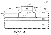
図4は、トランジスタ401の生成後のウエハ101の部分断面図を示す。トランジスタ401は、ゲート酸化物407上に形成されたゲート403を有する。ゲート酸化物407はストレインシリコン層305上に形成される。トランジスタ307は、層305の上方に形成されたスペーサ405をさらに有する。示された実施形態では、トランジスタ401は、例えば選択領域で層305および207にドーパントを注入することにより形成されたソース/ドレイン領域411および409を有する。トランジスタ401は、(示された実施形態では)ストレインドシリコン層305に形成されたチャネル領域413を有する。
FIG. 4 shows a partial cross-sectional view of the
別の実施形態では、テンプレート層材料は、シリコンゲルマニウム炭素、シリコンスズおよびゲルマニウム炭素中の炭素のような他の成分を含んでもよい。ウエハ101は他のトランジスタ(図示しない)を備えていてもよい。いくつかの実施形態では、層107がいくつかのウエハ101の領域に選択的に形成され得る。別の実施形態では、層107が全部のウエハ101の上に形成される。また、いくつかの実施形態では、凝縮プロセスが全部の層107に選択的に行なわれ得る。別の実施形態では、凝縮プロセスが他の領域がマスクされたウエハの選択領域に行なわれる。例えば、それは、層305は、Nチャネル領域とPチャネル領域とで異なる歪み特性を有することが望ましい場合がある。
In another embodiment, the template layer material may include other components such as silicon germanium carbon, silicon tin, and carbon in germanium carbon. The
1実施形態では、半導体構造を形成する方法は、セミコンダクター・オン・インシュレータ(SOI)構成を有するウエハを提供することを含む。ウエハは、絶縁体上に第1半導体層を備えている。第1半導体層は少なくとも2つの成分より形成されている。第1半導体層は、第1半導体層の第2部分に重なる第1部分を備えている。第1部分は少なくとも2つの成分のうちの第1濃度の第1成分を含み、第2部分は少なくとも2つの成分のうちの第2濃度の第1成分を含む。第1濃度は第2濃度よりも小さい。方法はさらに、第1半導体層上で凝縮プロセスを行い、第1半導体層の一部分を消費し、かつ第1半導体層の残りの部分の上に上記の少なくとも2つの成分のうちの第2成分を含む材料を形成することを含む。方法はさらに、材料を除去し、材料を除去した後に、残りの部分の上に第2成分を含む第2半導体層を形成することを含む。 In one embodiment, a method for forming a semiconductor structure includes providing a wafer having a semiconductor-on-insulator (SOI) configuration. The wafer includes a first semiconductor layer on an insulator. The first semiconductor layer is formed of at least two components. The first semiconductor layer includes a first portion that overlaps the second portion of the first semiconductor layer. The first portion includes a first component at a first concentration of at least two components, and the second portion includes a first component at a second concentration of at least two components. The first concentration is smaller than the second concentration. The method further includes performing a condensation process on the first semiconductor layer, consuming a portion of the first semiconductor layer, and applying a second component of the at least two components on the remaining portion of the first semiconductor layer. Forming a material comprising. The method further includes removing the material and, after removing the material, forming a second semiconductor layer including a second component over the remaining portion.
別の実施形態では、半導体構造を形成する方法は、ウエハを提供することを含む。ウエハは第1半導体層を備えている。第1半導体層はシリコンとゲルマニウムとを含む。第1半導体層は、第1濃度のゲルマニウムを有する第1部分と、第2濃度のゲルマニウムを有する第2部分とを備えている。第1部分は第2部分に重なっている。第1濃度は第2濃度よりも小さい。方法はさらに、第1半導体層上で凝縮プロセスを行い、第1半導体層の一部分を消費し、かつ第1半導体層の残りの部分に重なるシリコンを含む材料を形成することを含む。方法はさらに、シリコンを含む材料を除去し、シリコンを含む材料を除去した後に、残りの部分上にシリコンを含む第2半導体層を形成することを含む。 In another embodiment, a method for forming a semiconductor structure includes providing a wafer. The wafer includes a first semiconductor layer. The first semiconductor layer includes silicon and germanium. The first semiconductor layer includes a first portion having a first concentration of germanium and a second portion having a second concentration of germanium. The first part overlaps the second part. The first concentration is smaller than the second concentration. The method further includes performing a condensation process on the first semiconductor layer to form a material comprising silicon that consumes a portion of the first semiconductor layer and overlies the remaining portion of the first semiconductor layer. The method further includes removing the silicon-containing material, and after removing the silicon-containing material, forming a second semiconductor layer containing silicon on the remaining portion.
別の実施形態では、半導体装置を形成する方法は、セミコンダクター・オン・インシュレータ(SOI)構成を有するウエハを提供することを含む。ウエハは、絶縁体上に第1半導体層を備えている。第1半導体層はゲルマニウムとシリコンとを含んでいる。第1半導体層は、第1半導体層の第2部分に重なる第1半導体層の第1部分を含んでいる。第1部分は、第1濃度のゲルマニウムを含み、第2部分は、第2濃度のゲルマニウムを含む。第1濃度は第2濃度よりも小さい。方法はさらに、第1半導体層上で酸化プロセスを行い、第1半導体層の一部分を消費し、かつ第1半導体層の残りの部分の上に酸化物を形成することを含む。方法はさらに、酸化物を除去し、酸化物を除去した後に、残りの部分をテンプレート層として用いて残りの部分の上にシリコンを含む第2半導体層を形成することを含む。方法はさらに、チャネル領域を含むトランジスタを形成することを含む。チャネル領域の少なくとも一部分は第2半導体層に位置する。 In another embodiment, a method of forming a semiconductor device includes providing a wafer having a semiconductor-on-insulator (SOI) configuration. The wafer includes a first semiconductor layer on an insulator. The first semiconductor layer contains germanium and silicon. The first semiconductor layer includes a first portion of the first semiconductor layer that overlaps a second portion of the first semiconductor layer. The first portion includes a first concentration of germanium and the second portion includes a second concentration of germanium. The first concentration is smaller than the second concentration. The method further includes performing an oxidation process on the first semiconductor layer, consuming a portion of the first semiconductor layer, and forming an oxide on the remaining portion of the first semiconductor layer. The method further includes removing the oxide and, after removing the oxide, forming a second semiconductor layer comprising silicon over the remaining portion using the remaining portion as a template layer. The method further includes forming a transistor including a channel region. At least a portion of the channel region is located in the second semiconductor layer.
本発明の特定の実施形態を図示し説明してきたが、当業者であれば、本明細書の教示に基づけば、本発明とその寄り広い態様から逸脱することなくさらなる変更および改変が行えることが理解される。したがって、特許請求の範囲は、そのような変更および改変を本発明の真の趣旨および範囲内にあるものとして自身の範囲内に包含するものとする。 While particular embodiments of the present invention have been illustrated and described, those skilled in the art will be able to make further changes and modifications without departing from the invention and its broader aspects, based on the teachings herein. Understood. Accordingly, the claims are intended to cover within their scope such changes and modifications as fall within the true spirit and scope of this invention.
Claims (28)
セミコンダクター・オン・インシュレータ(SOI)構成を有するウエハを提供することと、ウエハは、絶縁体上に第1半導体層を備え、第1半導体層は少なくとも2つの成分より形成され、第1半導体層は、第1半導体層の第2部分に重なる第1部分を備え、第1部分は前記少なくとも2つの成分のうちの第1濃度の第1成分を含み、第2部分は少なくとも2つの成分のうちの第2濃度の第1成分を含み、第1濃度は第2濃度よりも小さいことと、
第1半導体層上で凝縮プロセスを行い、第1半導体層の一部分を消費し、かつ第1半導体層の残りの部分の上に前記少なくとも2つの成分のうちの第2成分を含む材料を形成することと、
材料を除去することと、
材料を除去した後に、残りの部分の上に第2成分を含む第2半導体層を形成することと、
を含む方法。 A method of forming a semiconductor structure comprising:
Providing a wafer having a semiconductor-on-insulator (SOI) configuration, the wafer comprising a first semiconductor layer on an insulator, the first semiconductor layer being formed of at least two components, the first semiconductor layer comprising: A first portion overlying the second portion of the first semiconductor layer, the first portion including a first concentration of the first component of the at least two components, and the second portion of the at least two components. Including a first component of a second concentration, wherein the first concentration is less than the second concentration;
A condensation process is performed on the first semiconductor layer to form a material that consumes a portion of the first semiconductor layer and that includes a second component of the at least two components on the remaining portion of the first semiconductor layer. And
Removing material,
Forming a second semiconductor layer including a second component on the remaining portion after removing the material;
Including methods.
ウエハを提供することと、ウエハは第1半導体層を備え、第1半導体層はシリコンとゲルマニウムとを含み、第1半導体層は、第1濃度のゲルマニウムを有する第1部分と、第2濃度のゲルマニウムを有する第2部分とを備え、第1部分は第2部分に重なっており、第1濃度は第2濃度よりも小さいことと、
第1半導体層上で凝縮プロセスを行い、第1半導体層の一部分を消費し、かつ第1半導体層の残りの部分に重なるシリコンを含む材料を形成することと、
シリコンを含む材料を除去することと、
シリコンを含む材料を除去した後に、残りの部分上にシリコンを含む第2半導体層を形成することと、を含む方法。 A method of forming a semiconductor structure comprising:
Providing a wafer, the wafer comprising a first semiconductor layer, the first semiconductor layer comprising silicon and germanium, the first semiconductor layer comprising a first portion having a first concentration of germanium, and a second concentration; A second portion having germanium, wherein the first portion overlaps the second portion, the first concentration is less than the second concentration;
Performing a condensation process on the first semiconductor layer, consuming a portion of the first semiconductor layer and forming a material comprising silicon overlying the remaining portion of the first semiconductor layer;
Removing material containing silicon;
Forming a second semiconductor layer comprising silicon on the remaining portion after removing the material comprising silicon.
セミコンダクター・オン・インシュレータ(SOI)構成を有するウエハを提供することと、ウエハは、絶縁体上に第1半導体層を備え、第1半導体層はゲルマニウムとシリコンとを含み、第1半導体層は、第1半導体層の第2部分に重なる第1半導体層の第1部分を含み、第1部分は第1濃度のゲルマニウムを含み、第2部分は第2濃度のゲルマニウムを含み、第1濃度は第2濃度よりも小さいことと、
第1半導体層上で酸化プロセスを行い、第1半導体層の一部分を消費し、かつ第1半導体層の残りの部分の上に酸化物を形成することと、
酸化物を除去することと、酸化物を除去した後に、残りの部分をテンプレート層として用いて残りの部分の上にシリコンを含む第2半導体層を形成することと、
チャネル領域の少なくとも一部分は第2半導体層に位置する、チャネル領域を含むトランジスタを形成することと、
を含む方法。 A method of forming a semiconductor device comprising:
Providing a wafer having a semiconductor-on-insulator (SOI) configuration, the wafer comprising a first semiconductor layer on an insulator, the first semiconductor layer comprising germanium and silicon, the first semiconductor layer comprising: The first portion of the first semiconductor layer overlies the second portion of the first semiconductor layer, the first portion includes a first concentration of germanium, the second portion includes a second concentration of germanium, and the first concentration is Less than 2 concentrations,
Performing an oxidation process on the first semiconductor layer, consuming a portion of the first semiconductor layer, and forming an oxide on the remaining portion of the first semiconductor layer;
Removing the oxide; after removing the oxide, forming a second semiconductor layer comprising silicon on the remaining portion using the remaining portion as a template layer;
Forming a transistor including the channel region, wherein at least a portion of the channel region is located in the second semiconductor layer;
Including methods.
Applications Claiming Priority (2)
| Application Number | Priority Date | Filing Date | Title |
|---|---|---|---|
| US10/919,952 US7241647B2 (en) | 2004-08-17 | 2004-08-17 | Graded semiconductor layer |
| PCT/US2005/029113 WO2006023492A1 (en) | 2004-08-17 | 2005-08-08 | Graded semiconductor layer |
Publications (2)
| Publication Number | Publication Date |
|---|---|
| JP2008510320A true JP2008510320A (en) | 2008-04-03 |
| JP2008510320A5 JP2008510320A5 (en) | 2008-09-25 |
Family
ID=35910124
Family Applications (1)
| Application Number | Title | Priority Date | Filing Date |
|---|---|---|---|
| JP2007527945A Pending JP2008510320A (en) | 2004-08-17 | 2005-08-08 | Gradient semiconductor layer |
Country Status (6)
| Country | Link |
|---|---|
| US (1) | US7241647B2 (en) |
| JP (1) | JP2008510320A (en) |
| KR (1) | KR20070047307A (en) |
| CN (1) | CN100472761C (en) |
| TW (1) | TWI371087B (en) |
| WO (1) | WO2006023492A1 (en) |
Families Citing this family (6)
| Publication number | Priority date | Publication date | Assignee | Title |
|---|---|---|---|---|
| DE102009010883B4 (en) * | 2009-02-27 | 2011-05-26 | Amd Fab 36 Limited Liability Company & Co. Kg | Adjusting a non-silicon content in a semiconductor alloy during FET transistor fabrication by an intermediate oxidation process |
| US8623728B2 (en) * | 2009-07-28 | 2014-01-07 | Taiwan Semiconductor Manufacturing Company, Ltd. | Method for forming high germanium concentration SiGe stressor |
| CN102903636B (en) * | 2011-07-25 | 2015-05-06 | 中芯国际集成电路制造(上海)有限公司 | Manufacturing method of MOS (metal oxide semiconductor) transistor |
| CN102903635B (en) * | 2011-07-25 | 2015-05-06 | 中芯国际集成电路制造(上海)有限公司 | Manufacturing method of MOS (metal oxide semiconductor) transistor |
| US20140057399A1 (en) * | 2012-08-24 | 2014-02-27 | International Business Machines Corporation | Using Fast Anneal to Form Uniform Ni(Pt)Si(Ge) Contacts on SiGe Layer |
| CN105679645A (en) * | 2014-11-17 | 2016-06-15 | 上海华力微电子有限公司 | Improvement method for dislocation defect in embedded SiGe epitaxy |
Citations (3)
| Publication number | Priority date | Publication date | Assignee | Title |
|---|---|---|---|---|
| JP2003031495A (en) * | 2001-07-12 | 2003-01-31 | Hitachi Ltd | Manufacturing method of semiconductor device substrate and semiconductor device |
| JP2003197544A (en) * | 2001-12-27 | 2003-07-11 | Sumitomo Mitsubishi Silicon Corp | Semiconductor substrate, field effect transistor, and their manufacturing methods |
| JP2005072054A (en) * | 2003-08-27 | 2005-03-17 | Toshiba Corp | METHOD FOR MANUFACTURING STRAIN RELAXING SiGe SUBSTRATE |
Family Cites Families (35)
| Publication number | Priority date | Publication date | Assignee | Title |
|---|---|---|---|---|
| US3912559A (en) | 1971-11-25 | 1975-10-14 | Suwa Seikosha Kk | Complementary MIS-type semiconductor devices and methods for manufacturing same |
| US4851257A (en) | 1987-03-13 | 1989-07-25 | Harris Corporation | Process for the fabrication of a vertical contact |
| US5461243A (en) | 1993-10-29 | 1995-10-24 | International Business Machines Corporation | Substrate for tensilely strained semiconductor |
| US5534713A (en) | 1994-05-20 | 1996-07-09 | International Business Machines Corporation | Complementary metal-oxide semiconductor transistor logic using strained SI/SIGE heterostructure layers |
| US5756898A (en) * | 1994-06-27 | 1998-05-26 | Texaco Inc. | Passive acoustic method of measuring the effective internal diameter of a pipe containing flowing fluids |
| DE59707274D1 (en) | 1996-09-27 | 2002-06-20 | Infineon Technologies Ag | Integrated CMOS circuit arrangement and method for its production |
| US5906951A (en) | 1997-04-30 | 1999-05-25 | International Business Machines Corporation | Strained Si/SiGe layers on insulator |
| US5846857A (en) | 1997-09-05 | 1998-12-08 | Advanced Micro Devices, Inc. | CMOS processing employing removable sidewall spacers for independently optimized N- and P-channel transistor performance |
| US5943565A (en) | 1997-09-05 | 1999-08-24 | Advanced Micro Devices, Inc. | CMOS processing employing separate spacers for independently optimized transistor performance |
| US6124627A (en) | 1998-12-03 | 2000-09-26 | Texas Instruments Incorporated | Lateral MOSFET having a barrier between the source/drain region and the channel region using a heterostructure raised source/drain region |
| US6259138B1 (en) | 1998-12-18 | 2001-07-10 | Semiconductor Energy Laboratory Co., Ltd. | Semiconductor device having multilayered gate electrode and impurity regions overlapping therewith |
| US6369438B1 (en) * | 1998-12-24 | 2002-04-09 | Kabushiki Kaisha Toshiba | Semiconductor device and method for manufacturing the same |
| JP3884203B2 (en) | 1998-12-24 | 2007-02-21 | 株式会社東芝 | Manufacturing method of semiconductor device |
| JP2001036054A (en) | 1999-07-19 | 2001-02-09 | Mitsubishi Electric Corp | Manufacture of soi substrate |
| US6339232B1 (en) | 1999-09-20 | 2002-01-15 | Kabushika Kaisha Toshiba | Semiconductor device |
| KR100392166B1 (en) * | 2000-03-17 | 2003-07-22 | 가부시끼가이샤 도시바 | Semiconductor device and method for manufacturing the same |
| US6524935B1 (en) | 2000-09-29 | 2003-02-25 | International Business Machines Corporation | Preparation of strained Si/SiGe on insulator by hydrogen induced layer transfer technique |
| US6890835B1 (en) | 2000-10-19 | 2005-05-10 | International Business Machines Corporation | Layer transfer of low defect SiGe using an etch-back process |
| US7312485B2 (en) | 2000-11-29 | 2007-12-25 | Intel Corporation | CMOS fabrication process utilizing special transistor orientation |
| US6649480B2 (en) | 2000-12-04 | 2003-11-18 | Amberwave Systems Corporation | Method of fabricating CMOS inverter and integrated circuits utilizing strained silicon surface channel MOSFETs |
| US20020100942A1 (en) | 2000-12-04 | 2002-08-01 | Fitzgerald Eugene A. | CMOS inverter and integrated circuits utilizing strained silicon surface channel MOSFETs |
| US20020168802A1 (en) | 2001-05-14 | 2002-11-14 | Hsu Sheng Teng | SiGe/SOI CMOS and method of making the same |
| US6855436B2 (en) | 2003-05-30 | 2005-02-15 | International Business Machines Corporation | Formation of silicon-germanium-on-insulator (SGOI) by an integral high temperature SIMOX-Ge interdiffusion anneal |
| US6475870B1 (en) | 2001-07-23 | 2002-11-05 | Taiwan Semiconductor Manufacturing Company | P-type LDMOS device with buried layer to solve punch-through problems and process for its manufacture |
| WO2003025984A2 (en) | 2001-09-21 | 2003-03-27 | Amberwave Systems Corporation | Semiconductor structures employing strained material layers with defined impurity gradients and methods for fabricating same |
| US6621131B2 (en) | 2001-11-01 | 2003-09-16 | Intel Corporation | Semiconductor transistor having a stressed channel |
| US6515335B1 (en) * | 2002-01-04 | 2003-02-04 | International Business Machines Corporation | Method for fabrication of relaxed SiGe buffer layers on silicon-on-insulators and structures containing the same |
| US6562703B1 (en) * | 2002-03-13 | 2003-05-13 | Sharp Laboratories Of America, Inc. | Molecular hydrogen implantation method for forming a relaxed silicon germanium layer with high germanium content |
| US6743651B2 (en) * | 2002-04-23 | 2004-06-01 | International Business Machines Corporation | Method of forming a SiGe-on-insulator substrate using separation by implantation of oxygen |
| US6638802B1 (en) | 2002-06-20 | 2003-10-28 | Intel Corporation | Forming strained source drain junction field effect transistors |
| JP3873012B2 (en) * | 2002-07-29 | 2007-01-24 | 株式会社東芝 | Manufacturing method of semiconductor device |
| US6955952B2 (en) | 2003-03-07 | 2005-10-18 | Taiwan Semiconductor Manufacturing Company, Ltd. | Strain balanced structure with a tensile strained silicon channel and a compressive strained silicon-germanium channel for CMOS performance enhancement |
| US7022593B2 (en) * | 2003-03-12 | 2006-04-04 | Asm America, Inc. | SiGe rectification process |
| US7026249B2 (en) * | 2003-05-30 | 2006-04-11 | International Business Machines Corporation | SiGe lattice engineering using a combination of oxidation, thinning and epitaxial regrowth |
| US7049660B2 (en) * | 2003-05-30 | 2006-05-23 | International Business Machines Corporation | High-quality SGOI by oxidation near the alloy melting temperature |
-
2004
- 2004-08-17 US US10/919,952 patent/US7241647B2/en not_active Expired - Fee Related
-
2005
- 2005-08-08 CN CNB2005800279288A patent/CN100472761C/en not_active Expired - Fee Related
- 2005-08-08 KR KR1020077003816A patent/KR20070047307A/en not_active Application Discontinuation
- 2005-08-08 JP JP2007527945A patent/JP2008510320A/en active Pending
- 2005-08-08 WO PCT/US2005/029113 patent/WO2006023492A1/en active Application Filing
- 2005-08-12 TW TW094127426A patent/TWI371087B/en not_active IP Right Cessation
Patent Citations (3)
| Publication number | Priority date | Publication date | Assignee | Title |
|---|---|---|---|---|
| JP2003031495A (en) * | 2001-07-12 | 2003-01-31 | Hitachi Ltd | Manufacturing method of semiconductor device substrate and semiconductor device |
| JP2003197544A (en) * | 2001-12-27 | 2003-07-11 | Sumitomo Mitsubishi Silicon Corp | Semiconductor substrate, field effect transistor, and their manufacturing methods |
| JP2005072054A (en) * | 2003-08-27 | 2005-03-17 | Toshiba Corp | METHOD FOR MANUFACTURING STRAIN RELAXING SiGe SUBSTRATE |
Also Published As
| Publication number | Publication date |
|---|---|
| CN101006580A (en) | 2007-07-25 |
| KR20070047307A (en) | 2007-05-04 |
| US7241647B2 (en) | 2007-07-10 |
| US20060040433A1 (en) | 2006-02-23 |
| WO2006023492A1 (en) | 2006-03-02 |
| CN100472761C (en) | 2009-03-25 |
| TWI371087B (en) | 2012-08-21 |
| TW200620572A (en) | 2006-06-16 |
Similar Documents
| Publication | Publication Date | Title |
|---|---|---|
| US7902008B2 (en) | Methods for fabricating a stressed MOS device | |
| US8557669B2 (en) | MOSFET device with localized stressor | |
| US7550758B2 (en) | Method for providing a nanoscale, high electron mobility transistor (HEMT) on insulator | |
| US7303966B2 (en) | Semiconductor device and method of manufacturing the same | |
| US7262465B2 (en) | P-channel MOS transistor and fabrication process thereof | |
| US20050148162A1 (en) | Method of preventing surface roughening during hydrogen pre-bake of SiGe substrates using chlorine containing gases | |
| US7022593B2 (en) | SiGe rectification process | |
| JP2008504678A (en) | Structure and method for fabricating PMOS devices in compressive strained Ge layers (integration of strained Ge into advanced CMOS technology) | |
| JP2010519734A (en) | Multi-layer source / drain stressor | |
| US7238588B2 (en) | Silicon buffered shallow trench isolation | |
| WO2005078786A1 (en) | Method of forming thin sgoi wafers with high relaxation and low stacking fault defect density | |
| JP2008510320A (en) | Gradient semiconductor layer | |
| US20070202669A1 (en) | Epitaxial growth method and semiconductor device fabrication method | |
| KR20070032692A (en) | A method of manufacturing a tensioned semiconductor layer, a method of manufacturing a semiconductor device, and a semiconductor substrate suitable for use in such a method. | |
| JP2010103142A (en) | Method for fabricating semiconductor device | |
| JP2010040931A (en) | Manufacturing method of semiconductor substrate, and semiconductor substrate | |
| JP5107936B2 (en) | Air break to improve silicide formation with composite cap | |
| EP3961721A1 (en) | Improved method for enriching germanium around the channel of a transistor | |
| US20060088966A1 (en) | Semiconductor device having a smooth EPI layer and a method for its manufacture | |
| CN111863593B (en) | Stress film with gradient distribution of chemical components, semiconductor device and forming method thereof | |
| JP2006228958A (en) | Semiconductor device and manufacturing method thereof | |
| Hikavyy et al. | Application of HCl gas phase etch in the production of novel devices | |
| JPH05315318A (en) | Formation of oxidized silicon film and manufacture of field-effect transistor using same | |
| JPH09181309A (en) | Vertical field-effect transistor and manufacture thereof |
Legal Events
| Date | Code | Title | Description |
|---|---|---|---|
| A521 | Written amendment |
Free format text: JAPANESE INTERMEDIATE CODE: A523 Effective date: 20080806 |
|
| A621 | Written request for application examination |
Free format text: JAPANESE INTERMEDIATE CODE: A621 Effective date: 20080806 |
|
| A977 | Report on retrieval |
Free format text: JAPANESE INTERMEDIATE CODE: A971007 Effective date: 20111128 |
|
| A131 | Notification of reasons for refusal |
Free format text: JAPANESE INTERMEDIATE CODE: A131 Effective date: 20111206 |
|
| A02 | Decision of refusal |
Free format text: JAPANESE INTERMEDIATE CODE: A02 Effective date: 20120508 |