EP3961721A1 - Improved method for enriching germanium around the channel of a transistor - Google Patents
Improved method for enriching germanium around the channel of a transistor Download PDFInfo
- Publication number
- EP3961721A1 EP3961721A1 EP21188650.2A EP21188650A EP3961721A1 EP 3961721 A1 EP3961721 A1 EP 3961721A1 EP 21188650 A EP21188650 A EP 21188650A EP 3961721 A1 EP3961721 A1 EP 3961721A1
- Authority
- EP
- European Patent Office
- Prior art keywords
- semiconductor
- layer
- blocks
- silicon
- spacers
- Prior art date
- Legal status (The legal status is an assumption and is not a legal conclusion. Google has not performed a legal analysis and makes no representation as to the accuracy of the status listed.)
- Pending
Links
- 229910052732 germanium Inorganic materials 0.000 title claims abstract description 32
- GNPVGFCGXDBREM-UHFFFAOYSA-N germanium atom Chemical compound [Ge] GNPVGFCGXDBREM-UHFFFAOYSA-N 0.000 title claims abstract description 30
- 238000000034 method Methods 0.000 title claims description 21
- 239000004065 semiconductor Substances 0.000 claims abstract description 108
- 229910052710 silicon Inorganic materials 0.000 claims abstract description 28
- 125000006850 spacer group Chemical group 0.000 claims abstract description 27
- XUIMIQQOPSSXEZ-UHFFFAOYSA-N Silicon Chemical compound [Si] XUIMIQQOPSSXEZ-UHFFFAOYSA-N 0.000 claims abstract description 26
- 238000007254 oxidation reaction Methods 0.000 claims abstract description 25
- 230000003647 oxidation Effects 0.000 claims abstract description 24
- 239000010703 silicon Substances 0.000 claims abstract description 24
- 238000004519 manufacturing process Methods 0.000 claims abstract description 13
- 239000012212 insulator Substances 0.000 claims abstract description 11
- 239000000463 material Substances 0.000 claims description 45
- 239000000758 substrate Substances 0.000 claims description 8
- 230000015572 biosynthetic process Effects 0.000 claims description 6
- 238000000151 deposition Methods 0.000 claims description 6
- 238000011065 in-situ storage Methods 0.000 claims description 6
- 238000000137 annealing Methods 0.000 claims description 4
- 230000008021 deposition Effects 0.000 claims description 4
- 230000007935 neutral effect Effects 0.000 claims description 3
- 239000010410 layer Substances 0.000 description 46
- 229910000577 Silicon-germanium Inorganic materials 0.000 description 9
- 239000002344 surface layer Substances 0.000 description 9
- 238000000407 epitaxy Methods 0.000 description 8
- 230000006835 compression Effects 0.000 description 3
- 238000007906 compression Methods 0.000 description 3
- 238000009833 condensation Methods 0.000 description 3
- 230000005494 condensation Effects 0.000 description 3
- 229910004298 SiO 2 Inorganic materials 0.000 description 2
- LEVVHYCKPQWKOP-UHFFFAOYSA-N [Si].[Ge] Chemical compound [Si].[Ge] LEVVHYCKPQWKOP-UHFFFAOYSA-N 0.000 description 2
- 238000004140 cleaning Methods 0.000 description 2
- 239000013078 crystal Substances 0.000 description 2
- 230000003247 decreasing effect Effects 0.000 description 2
- 230000004048 modification Effects 0.000 description 2
- 238000012986 modification Methods 0.000 description 2
- 238000002360 preparation method Methods 0.000 description 2
- 230000001737 promoting effect Effects 0.000 description 2
- ZOXJGFHDIHLPTG-UHFFFAOYSA-N Boron Chemical compound [B] ZOXJGFHDIHLPTG-UHFFFAOYSA-N 0.000 description 1
- VYPSYNLAJGMNEJ-UHFFFAOYSA-N Silicium dioxide Chemical compound O=[Si]=O VYPSYNLAJGMNEJ-UHFFFAOYSA-N 0.000 description 1
- 229910020751 SixGe1-x Inorganic materials 0.000 description 1
- ATJFFYVFTNAWJD-UHFFFAOYSA-N Tin Chemical compound [Sn] ATJFFYVFTNAWJD-UHFFFAOYSA-N 0.000 description 1
- 238000000560 X-ray reflectometry Methods 0.000 description 1
- 230000005540 biological transmission Effects 0.000 description 1
- 229910052796 boron Inorganic materials 0.000 description 1
- 239000000969 carrier Substances 0.000 description 1
- 150000001875 compounds Chemical class 0.000 description 1
- 239000002178 crystalline material Substances 0.000 description 1
- 238000009792 diffusion process Methods 0.000 description 1
- 239000002019 doping agent Substances 0.000 description 1
- 238000001312 dry etching Methods 0.000 description 1
- 230000000694 effects Effects 0.000 description 1
- 238000005538 encapsulation Methods 0.000 description 1
- 238000005530 etching Methods 0.000 description 1
- 150000002290 germanium Chemical class 0.000 description 1
- 238000010438 heat treatment Methods 0.000 description 1
- 229910052739 hydrogen Inorganic materials 0.000 description 1
- 239000001257 hydrogen Substances 0.000 description 1
- 230000008018 melting Effects 0.000 description 1
- 238000002844 melting Methods 0.000 description 1
- 239000002184 metal Substances 0.000 description 1
- 229910021420 polycrystalline silicon Inorganic materials 0.000 description 1
- 229920005591 polysilicon Polymers 0.000 description 1
- 239000002243 precursor Substances 0.000 description 1
- 229910052814 silicon oxide Inorganic materials 0.000 description 1
Images

Classifications
-
- H—ELECTRICITY
- H01—ELECTRIC ELEMENTS
- H01L—SEMICONDUCTOR DEVICES NOT COVERED BY CLASS H10
- H01L29/00—Semiconductor devices adapted for rectifying, amplifying, oscillating or switching, or capacitors or resistors with at least one potential-jump barrier or surface barrier, e.g. PN junction depletion layer or carrier concentration layer; Details of semiconductor bodies or of electrodes thereof ; Multistep manufacturing processes therefor
- H01L29/66—Types of semiconductor device ; Multistep manufacturing processes therefor
- H01L29/66007—Multistep manufacturing processes
- H01L29/66075—Multistep manufacturing processes of devices having semiconductor bodies comprising group 14 or group 13/15 materials
- H01L29/66227—Multistep manufacturing processes of devices having semiconductor bodies comprising group 14 or group 13/15 materials the devices being controllable only by the electric current supplied or the electric potential applied, to an electrode which does not carry the current to be rectified, amplified or switched, e.g. three-terminal devices
- H01L29/66409—Unipolar field-effect transistors
- H01L29/66477—Unipolar field-effect transistors with an insulated gate, i.e. MISFET
- H01L29/66742—Thin film unipolar transistors
- H01L29/66772—Monocristalline silicon transistors on insulating substrates, e.g. quartz substrates
-
- H—ELECTRICITY
- H01—ELECTRIC ELEMENTS
- H01L—SEMICONDUCTOR DEVICES NOT COVERED BY CLASS H10
- H01L21/00—Processes or apparatus adapted for the manufacture or treatment of semiconductor or solid state devices or of parts thereof
- H01L21/02—Manufacture or treatment of semiconductor devices or of parts thereof
- H01L21/02104—Forming layers
- H01L21/02107—Forming insulating materials on a substrate
- H01L21/02225—Forming insulating materials on a substrate characterised by the process for the formation of the insulating layer
- H01L21/02227—Forming insulating materials on a substrate characterised by the process for the formation of the insulating layer formation by a process other than a deposition process
- H01L21/0223—Forming insulating materials on a substrate characterised by the process for the formation of the insulating layer formation by a process other than a deposition process formation by oxidation, e.g. oxidation of the substrate
- H01L21/02233—Forming insulating materials on a substrate characterised by the process for the formation of the insulating layer formation by a process other than a deposition process formation by oxidation, e.g. oxidation of the substrate of the semiconductor substrate or a semiconductor layer
- H01L21/02236—Forming insulating materials on a substrate characterised by the process for the formation of the insulating layer formation by a process other than a deposition process formation by oxidation, e.g. oxidation of the substrate of the semiconductor substrate or a semiconductor layer group IV semiconductor
-
- H—ELECTRICITY
- H01—ELECTRIC ELEMENTS
- H01L—SEMICONDUCTOR DEVICES NOT COVERED BY CLASS H10
- H01L21/00—Processes or apparatus adapted for the manufacture or treatment of semiconductor or solid state devices or of parts thereof
- H01L21/02—Manufacture or treatment of semiconductor devices or of parts thereof
- H01L21/02104—Forming layers
- H01L21/02365—Forming inorganic semiconducting materials on a substrate
- H01L21/02518—Deposited layers
- H01L21/02521—Materials
- H01L21/02524—Group 14 semiconducting materials
- H01L21/02532—Silicon, silicon germanium, germanium
-
- H—ELECTRICITY
- H01—ELECTRIC ELEMENTS
- H01L—SEMICONDUCTOR DEVICES NOT COVERED BY CLASS H10
- H01L29/00—Semiconductor devices adapted for rectifying, amplifying, oscillating or switching, or capacitors or resistors with at least one potential-jump barrier or surface barrier, e.g. PN junction depletion layer or carrier concentration layer; Details of semiconductor bodies or of electrodes thereof ; Multistep manufacturing processes therefor
- H01L29/02—Semiconductor bodies ; Multistep manufacturing processes therefor
- H01L29/12—Semiconductor bodies ; Multistep manufacturing processes therefor characterised by the materials of which they are formed
- H01L29/16—Semiconductor bodies ; Multistep manufacturing processes therefor characterised by the materials of which they are formed including, apart from doping materials or other impurities, only elements of Group IV of the Periodic System
- H01L29/161—Semiconductor bodies ; Multistep manufacturing processes therefor characterised by the materials of which they are formed including, apart from doping materials or other impurities, only elements of Group IV of the Periodic System including two or more of the elements provided for in group H01L29/16, e.g. alloys
- H01L29/165—Semiconductor bodies ; Multistep manufacturing processes therefor characterised by the materials of which they are formed including, apart from doping materials or other impurities, only elements of Group IV of the Periodic System including two or more of the elements provided for in group H01L29/16, e.g. alloys in different semiconductor regions, e.g. heterojunctions
-
- H—ELECTRICITY
- H01—ELECTRIC ELEMENTS
- H01L—SEMICONDUCTOR DEVICES NOT COVERED BY CLASS H10
- H01L29/00—Semiconductor devices adapted for rectifying, amplifying, oscillating or switching, or capacitors or resistors with at least one potential-jump barrier or surface barrier, e.g. PN junction depletion layer or carrier concentration layer; Details of semiconductor bodies or of electrodes thereof ; Multistep manufacturing processes therefor
- H01L29/66—Types of semiconductor device ; Multistep manufacturing processes therefor
- H01L29/66007—Multistep manufacturing processes
- H01L29/66075—Multistep manufacturing processes of devices having semiconductor bodies comprising group 14 or group 13/15 materials
- H01L29/66227—Multistep manufacturing processes of devices having semiconductor bodies comprising group 14 or group 13/15 materials the devices being controllable only by the electric current supplied or the electric potential applied, to an electrode which does not carry the current to be rectified, amplified or switched, e.g. three-terminal devices
- H01L29/66409—Unipolar field-effect transistors
- H01L29/66477—Unipolar field-effect transistors with an insulated gate, i.e. MISFET
- H01L29/66553—Unipolar field-effect transistors with an insulated gate, i.e. MISFET using inside spacers, permanent or not
-
- H—ELECTRICITY
- H01—ELECTRIC ELEMENTS
- H01L—SEMICONDUCTOR DEVICES NOT COVERED BY CLASS H10
- H01L29/00—Semiconductor devices adapted for rectifying, amplifying, oscillating or switching, or capacitors or resistors with at least one potential-jump barrier or surface barrier, e.g. PN junction depletion layer or carrier concentration layer; Details of semiconductor bodies or of electrodes thereof ; Multistep manufacturing processes therefor
- H01L29/66—Types of semiconductor device ; Multistep manufacturing processes therefor
- H01L29/66007—Multistep manufacturing processes
- H01L29/66075—Multistep manufacturing processes of devices having semiconductor bodies comprising group 14 or group 13/15 materials
- H01L29/66227—Multistep manufacturing processes of devices having semiconductor bodies comprising group 14 or group 13/15 materials the devices being controllable only by the electric current supplied or the electric potential applied, to an electrode which does not carry the current to be rectified, amplified or switched, e.g. three-terminal devices
- H01L29/66409—Unipolar field-effect transistors
- H01L29/66477—Unipolar field-effect transistors with an insulated gate, i.e. MISFET
- H01L29/66568—Lateral single gate silicon transistors
- H01L29/66613—Lateral single gate silicon transistors with a gate recessing step, e.g. using local oxidation
- H01L29/66628—Lateral single gate silicon transistors with a gate recessing step, e.g. using local oxidation recessing the gate by forming single crystalline semiconductor material at the source or drain location
-
- H—ELECTRICITY
- H01—ELECTRIC ELEMENTS
- H01L—SEMICONDUCTOR DEVICES NOT COVERED BY CLASS H10
- H01L29/00—Semiconductor devices adapted for rectifying, amplifying, oscillating or switching, or capacitors or resistors with at least one potential-jump barrier or surface barrier, e.g. PN junction depletion layer or carrier concentration layer; Details of semiconductor bodies or of electrodes thereof ; Multistep manufacturing processes therefor
- H01L29/66—Types of semiconductor device ; Multistep manufacturing processes therefor
- H01L29/68—Types of semiconductor device ; Multistep manufacturing processes therefor controllable by only the electric current supplied, or only the electric potential applied, to an electrode which does not carry the current to be rectified, amplified or switched
- H01L29/76—Unipolar devices, e.g. field effect transistors
- H01L29/772—Field effect transistors
- H01L29/78—Field effect transistors with field effect produced by an insulated gate
- H01L29/7842—Field effect transistors with field effect produced by an insulated gate means for exerting mechanical stress on the crystal lattice of the channel region, e.g. using a flexible substrate
- H01L29/7848—Field effect transistors with field effect produced by an insulated gate means for exerting mechanical stress on the crystal lattice of the channel region, e.g. using a flexible substrate the means being located in the source/drain region, e.g. SiGe source and drain
-
- H—ELECTRICITY
- H01—ELECTRIC ELEMENTS
- H01L—SEMICONDUCTOR DEVICES NOT COVERED BY CLASS H10
- H01L29/00—Semiconductor devices adapted for rectifying, amplifying, oscillating or switching, or capacitors or resistors with at least one potential-jump barrier or surface barrier, e.g. PN junction depletion layer or carrier concentration layer; Details of semiconductor bodies or of electrodes thereof ; Multistep manufacturing processes therefor
- H01L29/66—Types of semiconductor device ; Multistep manufacturing processes therefor
- H01L29/68—Types of semiconductor device ; Multistep manufacturing processes therefor controllable by only the electric current supplied, or only the electric potential applied, to an electrode which does not carry the current to be rectified, amplified or switched
- H01L29/76—Unipolar devices, e.g. field effect transistors
- H01L29/772—Field effect transistors
- H01L29/78—Field effect transistors with field effect produced by an insulated gate
- H01L29/786—Thin film transistors, i.e. transistors with a channel being at least partly a thin film
- H01L29/78651—Silicon transistors
- H01L29/78654—Monocrystalline silicon transistors
Definitions
- the present description relates to the field of transistor structures, and more particularly those provided with a channel zone undergoing a deformation or mechanical stress.
- mechanical deformation is meant a material which has its crystal lattice parameter(s) elongated or shortened.
- the deformed lattice parameter is greater than the so-called “natural” parameter of a crystalline material, this is said to be in tension deformation.
- the deformed lattice parameter is smaller than the natural lattice parameter, the material is said to be in compressive strain or compression.
- a stress applied to a semiconductor material induces a modification of the crystal lattice and therefore of its band structure, which will result in a modification of the mobility of the carriers in this material.
- the mobility of the electrons is increased (respectively decreased) by a longitudinal stress in tension (respectively in compression) of the semiconductor material in which they transit whereas the mobility of the holes will be increased (respectively decreased) when the semiconductor is in compression (respectively in tension) in the longitudinal direction.
- the document US 2008/0042209 A1 thus presents a method for producing, on a 1 SOI substrate, a transistor having a channel structure formed in a surface layer of silicon which has just been put under stress.
- This stressing is carried out by means of a growth of SiGe on the surface layer then by carrying out an enrichment in Germanium of regions of the surface layer on either side of the channel region.
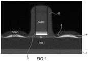
- pinch zones 6 where the thickness of semiconductor material is reduced may tend to form on either side of a region 3 of the surface layer located opposite grid and spacers 5.
- Such pinching zones 6 between this region 3 and portions 4 enriched in Germanium are illustrated on the figure 1 and pose several problems.
- the deposition of the silicon layer on the semiconductor blocks is carried out so as to completely fill said cavities.
- the growth of the second semiconductor material based on Si x Ge 1-x is carried out without doping.
- the semiconductor blocks are not doped when the thermal oxidation is carried out.
- the second semiconductor material may be different from the first semiconductor material and have a lattice parameter different from that of the first semiconductor material.
- At least one thermal annealing is carried out under a neutral atmosphere, so as to homogenize the germanium concentration of the semiconductor portions.
- the transistor produced is typically a P-type transistor.
- the Germanium-enriched semiconductor portions then make it possible to exert a compressive stress on the given region in which the channel structure is provided.
- This structure comprises a substrate of the semiconductor-on-insulator type, with a semiconductor support layer 10, typically made of silicon, an insulating layer 11 of silicon oxide arranged on the support layer 10 and a superficial semiconductor layer 12 arranged on and in contact with the insulating layer 11 and designed to receive at least one channel region of a transistor, in particular a P-type transistor, for example a PMOS.
- a semiconductor support layer 10 typically made of silicon
- an insulating layer 11 of silicon oxide arranged on the support layer 10
- a superficial semiconductor layer 12 arranged on and in contact with the insulating layer 11 and designed to receive at least one channel region of a transistor, in particular a P-type transistor, for example a PMOS.
- Gate block 22 may here be intended to form the final gate electrode of the transistor.
- Gate block 22 may for example be based on polysilicon or TiN or W or a combination of these materials.
- the spacers 23 may for example be based on SiN or SiCO or SiBCN or SiOCN or a combination of these materials.
- gate block 22 is also surmounted by at least one hard mask 24, for example formed from a layer of SiN and/or SiO 2 .
- a second semiconductor material, containing Germanium, is then grown by epitaxy on the first semiconductor material of said superficial semiconductor layer 12, which is intended to enrich the surface layer 12 with germanium.
- the second semiconductor material may be different from the first semiconductor material and have a lattice parameter different from that of the first semiconductor material.
- the second semiconductor material can be based on Si 1-x Ge x with x>0.
- the Germanium concentration x is for example between 0.05 and 0.80 and typically between 0.2 and 0.5, preferably such that x>a when the first semiconductor material is Si 1-a Ge a .
- the growth of the second semiconductor material on the first semiconductor material is typically carried out so as to form blocks 26 of the second semiconductor material having lateral facets 27 forming a non-zero angle ⁇ with a normal n at a principal plane of the surface layer (ie a plane passing through the surface layer and parallel to the plane [O; x; y] of the orthogonal reference [O; x; y; z] given on the figure 2B ).
- the growth epitaxial of this second material is preferably carried out without doping in situ so that the blocks 26 are not doped at this stage of the process.
- the blocks 26 are formed by selective epitaxy without covering the spacers 23 or the gate 22.
- the lateral facets 27 have one end located at the foot of the spacers 23.
- spaces or cavities 28 are arranged between the spacers 23 and the facets 27 of the blocks 26 of the second semiconductor material.
- these cavities 28 are then at least partially filled with the aid of a semiconductor layer 29.
- the semiconductor layer 29 is produced by deposition, in particular by epitaxial growth on the blocks 26.
- the layer 29 is at based on a material different from that of the semiconductor blocks 26 and in particular with a lower germanium concentration than that of the semiconductor blocks 26.
- the semiconductor material of the layer 29 is preferably chosen so as to be able to grow without making a facet.
- the semiconductor material of layer 29 may be silicon.
- the formation of this layer 29 can be such that portions can extend over the upper faces of the blocks 26.
- the growth of this material can optionally be carried out so that portions 29a of the layer 29 completely fill the cavities 28 ( Fig. 2C ).
- the semiconductor layer 29 is formed selectively without covering the gate 22. This epitaxial growth of the semiconductor layer 29 is preferably carried out without doping in situ.
- At least a first thermal oxidation step is carried out at a temperature that is preferably high but lower than the melting temperature of the material Si 1-x Ge x , typically at a temperature between 750° C. and 1100°C.
- the oxidation time/temperature pair depends on the thickness of the layer to be oxidized. For example, provision can be made to carry out the oxidation at a temperature of 900° C. for a period of the order of 5 min, or else at a temperature of 1050° C. for a period of the order of 20 s, for a layer with a thickness of about 6 nm of SiGe with a Germanium concentration of about 30%.
- the oxidation of the entire thickness of portions of the layer 29 located on the upper faces of blocks 26 while other portions 29a of the layer 29 which come to fill the cavities 28 and separating the side facets 27 of the spacers 23 are not yet oxidized.
- the semiconductor blocks 26 and the portions 29a then have different oxidation rates due to their respective different silicon proportions, as described in the document : “Si and SiGe: SiGe oxidation kinetics and oxide density measured by resonant soft X-ray reflectivity”, Rozé et al., Nanotechnology Material and Devices Conference 2017 .
- the oxidation is continued over the entire thickness of the blocks 26 then preferably so as to oxidize the portions 29a.
- the Germanium concentration is favored in portions 12a of the surface layer 12 further away than those directly adjacent to the access regions 12b ( figure 2E ). Because the oxidation rate depends on the Germanium content, with such an arrangement, a pinching effect as mentioned above and illustrated in the figure is avoided. figure 1 , likely to cause a discontinuity of the superficial semiconductor layer 12 and in any case to increase the channel access resistances.
- the portions 31a of lower germanium composition even typically have a greater thickness than that of parts 31b farther from the channel structure and can be produced with a thickness at least equal to or even greater than that of the access regions 12b and of the channel structure 12a.
- a deoxidation in order to remove a thickness of oxide 33 formed during the Germanium condensation can then be carried out ( figure 2F ).
- This removal can be carried out, for example, using dilute HF, with a content of, for example, 1%.
- semiconductor regions 35 can be grown by epitaxy on either side of the spacers 23 from the semiconductor portions 31a, 31b ( figure 2G ).
- a semiconductor material capable of promoting compressive stress in the channel structure is chosen.
- the semiconductor regions 35 are made of silicon germanium, preferably doped, for example with boron. In situ doping performed during the growth of the semiconductor material can be performed. A dose for example of the order of 1 e 20 at*cm ⁇ 3 can be used, for example.
- a P-type transistor formed in the Germanium-enriched superficial semiconductor layer of a semiconductor-on-insulator type substrate is particularly suitable for the implementation of circuits with low consumption (“Low Power”) and high performance (“high-performance”).
Abstract
Réalisation d'une structure de transistor comprenant dans cet ordre :- former sur la couche semi-conductrice superficielle et de part et d'autre d'espaceurs isolants, des blocs semi-conducteurs en Si<sub>x</sub>Ge<sub>1-x</sub>, les blocs semi-conducteurs ayant des facettes latérales,- croissance d'une couche à base de silicium sur les blocs semi-conducteurs, de manière à remplir des cavités situées entre lesdites facettes et lesdits espaceurs isolants,- oxydation thermique pour effectuer un enrichissement en germanium de portions semi-conductrices (31a, 31b) de la couche semi-conductrice superficielle (12) disposées de part et d'autre des espaceurs.Production of a transistor structure comprising in this order:- forming on the surface semiconductor layer and on either side of insulating spacers, semiconductor blocks in Si<sub>x</sub>Ge< sub>1-x</sub>, the semiconductor blocks having side facets,- growing a silicon-based layer on the semiconductor blocks, so as to fill cavities between said facets and said spacers insulators, - thermal oxidation to carry out germanium enrichment of semiconductor portions (31a, 31b) of surface semiconductor layer (12) arranged on either side of the spacers.
Description
La présente description concerne le domaine des structures de transistors, et plus particulièrement celles dotées d'une zone de canal subissant une déformation ou contrainte mécanique.The present description relates to the field of transistor structures, and more particularly those provided with a channel zone undergoing a deformation or mechanical stress.
Par déformation mécanique on entend un matériau qui a son ou ses paramètre(s) de maille cristalline allongé(s) ou écourté(s).By mechanical deformation is meant a material which has its crystal lattice parameter(s) elongated or shortened.
Dans le cas où le paramètre de maille déformé est plus important que le paramètre dit « naturel » d'un matériau cristallin, celui-ci est dit en déformation en tension. Lorsque le paramètre de maille déformé est plus petit que le paramètre de maille naturel, le matériau est dit en déformation compressive ou en compression.In the case where the deformed lattice parameter is greater than the so-called “natural” parameter of a crystalline material, this is said to be in tension deformation. When the deformed lattice parameter is smaller than the natural lattice parameter, the material is said to be in compressive strain or compression.
A ces états de déformation mécanique, on associe des états de contraintes mécaniques. Pour autant, il est également commun de se référer à ces états de déformation comme des états de contraintes mécaniques. Dans la suite de la présente demande, cette notion de déformation (« strain » selon la terminologie anglo-saxonne) sera désignée de façon générique par le terme « contrainte ».With these states of mechanical deformation, one associates states of mechanical constraints. However, it is also common to refer to these deformation states as mechanical stress states. In the rest of the present application, this notion of deformation (“strain” according to the Anglo-Saxon terminology) will be designated generically by the term “constraint”.
Une contrainte appliquée à un matériau semi-conducteur induit une modification de la maille cristalline et donc de sa structure de bande, dont va découler une modification de la mobilité des porteurs dans ce matériau.A stress applied to a semiconductor material induces a modification of the crystal lattice and therefore of its band structure, which will result in a modification of the mobility of the carriers in this material.
La mobilité des électrons est augmentée (respectivement diminuée) par une contrainte longitudinale en tension (respectivement en compression) du matériau semi-conducteur dans lequel ils transitent alors que la mobilité des trous sera augmentée (respectivement diminuée) lorsque le semi-conducteur est en compression (respectivement en tension) dans la direction longitudinale.The mobility of the electrons is increased (respectively decreased) by a longitudinal stress in tension (respectively in compression) of the semiconductor material in which they transit whereas the mobility of the holes will be increased (respectively decreased) when the semiconductor is in compression (respectively in tension) in the longitudinal direction.
Pour améliorer les performances des transistors de type P, il est connu de prévoir une structure de canal formée dans une couche superficielle contrainte en compression d'un substrat de type semi-conducteur isolant.To improve the performance of P-type transistors, it is known to provide a channel structure formed in a compressively strained surface layer of an insulating semiconductor-type substrate.
Le document
Elles peuvent tout d'abord limiter voire empêcher la transmission de la contrainte vers la région de canal.First of all, they can limit or even prevent the transmission of the stress to the channel region.
Elles peuvent également gêner la formation ultérieure de blocs de source et de drain en étant à l'origine de phénomènes de démouillage d'une épaisseur semi-conductrice que l'on réalise ensuite typiquement par épitaxie pour former ces blocs.They can also hinder the subsequent formation of source and drain blocks by being the cause of phenomena of dewetting of a semiconductor thickness which is then typically carried out by epitaxy to form these blocks.
Elles peuvent enfin créer une discontinuité électrique de blocs de source et de drain vers le canal ou tout du moins augmenter les résistances d'accès au canal.Finally, they can create an electrical discontinuity of source and drain blocks towards the channel or at the very least increase the access resistances to the channel.
Il se pose le problème de trouver un nouveau procédé de réalisation d'une structure de transistor contraint et qui soit amélioré vis-à-vis d'inconvénients énoncés ci-dessus.The problem arises of finding a new method for producing a strained transistor structure which is improved with respect to the drawbacks set out above.
Un mode de réalisation de la présente invention prévoit un procédé de réalisation d'une structure de transistor comprenant, dans cet ordre :
- fournir un bloc de grille et des espaceurs isolants de part et d'autre du bloc de grille sur une région donnée d'une couche semi-conductrice superficielle d'un substrat de type semi-conducteur sur isolant, la couche semi-conductrice superficielle étant à base d'un premier matériau semi-conducteur, en particulier du Si ou du Si1-aGea avec a > 0, la région donnée étant apte à accueillir une structure de canal dudit transistor en regard dudit bloc de grille,
- former sur la couche semi-conductrice superficielle et de part et d'autre des espaceurs, des blocs semi-conducteurs par croissance d'un deuxième matériau semi-conducteur à base de SixGe1-x, avec x > 0, les blocs semi-conducteurs ayant des facettes latérales réalisant un angle non-nul avec une normale à la couche semi-conductrice superficielle, les facettes latérales définissant des cavités entre les facettes et les espaceurs isolants,
- dépôt, en particulier par croissance d'une couche en silicium sur les blocs semi-conducteurs, de manière à remplir les cavités situées entre les facettes et les espaceurs isolants,
- oxydation thermique des blocs semi-conducteurs et de la couche de silicium, de sorte à réaliser un enrichissement en germanium d'une partie de la couche semi-conductrice superficielle, cette partie étant disposée autour du canal et des espaceurs.
- providing a gate block and insulating spacers on either side of the gate block on a given region of a surface semiconductor layer of a semiconductor-on-insulator substrate, the surface semiconductor layer being based on a first semiconductor material, in particular Si or Si 1-a Ge a with a > 0, the given region being able to accommodate a channel structure of said transistor facing said gate block,
- forming on the superficial semiconductor layer and on either side of the spacers, semiconductor blocks by growth of a second semiconductor material based on Si x Ge 1-x , with x > 0, the blocks semiconductors having lateral facets forming a non-zero angle with a normal to the surface semiconductor layer, the lateral facets defining cavities between the facets and the insulating spacers,
- deposition, in particular by growth, of a layer of silicon on the semiconductor blocks, so as to fill the cavities located between the facets and the insulating spacers,
- thermal oxidation of the semiconductor blocks and of the silicon layer, so as to achieve germanium enrichment of part of the superficial semiconductor layer, this part being arranged around the channel and the spacers.
Du fait de la présence de la couche en silicium et de son agencement par rapport aux blocs semi-conducteurs à base de SixGe1-x, on obtient à l'issue de l'oxydation thermique, un enrichissement en germanium desdites portions sans phénomène de pincement intempestif voire même sans que l'épaisseur de ces portions ne soit réduite par rapport aux régions d'accès au canal. Cela permet ainsi de limiter les résistances d'accès, d'appliquer une meilleure contrainte à la structure de canal et de favoriser une reprise d'épitaxie ultérieure lors de la réalisation des blocs de source et de drain.Due to the presence of the silicon layer and its arrangement with respect to the semiconductor blocks based on Si x Ge 1-x , one obtains at the end of the thermal oxidation, an enrichment in germanium of the said portions without phenomenon of untimely pinching, even without the thickness of these portions being reduced with respect to the regions of access to the channel. This thus makes it possible to limit the access resistances, to apply a better constraint to the channel structure and to promote a subsequent resumption of epitaxy during the production of the source and drain blocks.
Avantageusement, le dépôt de la couche en silicium sur les blocs semi-conducteurs est réalisé de manière à remplir entièrement lesdites cavités.Advantageously, the deposition of the silicon layer on the semiconductor blocks is carried out so as to completely fill said cavities.
Avantageusement, la croissance du deuxième matériau semi-conducteur à base de SixGe1-x est réalisée sans dopage. Ainsi, les blocs semi-conducteurs ne sont pas dopés lorsque l'oxydation thermique est effectuée.Advantageously, the growth of the second semiconductor material based on Si x Ge 1-x is carried out without doping. Thus, the semiconductor blocks are not doped when the thermal oxidation is carried out.
Avantageusement, la croissance de la couche à base de silicium sur les blocs semi-conducteurs, est réalisée sans dopage. Ainsi, la couche à base de silicium n'est pas dopée lorsque l'oxydation thermique est effectuée.Advantageously, the growth of the silicon-based layer on the semiconductor blocks is carried out without doping. Thus, the silicon-based layer is not doped when the thermal oxidation is carried out.
Le deuxième matériau semi-conducteur peut être différent du premier matériau semi-conducteur et avoir un paramètre de maille différent de celui du premier matériau semi-conducteur.The second semiconductor material may be different from the first semiconductor material and have a lattice parameter different from that of the first semiconductor material.
Selon une mise en œuvre particulière du procédé pour laquelle l'oxydation thermique conduit à la formation d'une couche d'oxyde sur les blocs semi-conducteurs, le procédé peut comprendre en outre des étapes de :
- retrait de la couche d'oxyde,
- croissance de matériau semi-conducteur sur les portions semi-conductrices de la couche semi-conductrice superficielle disposées de part et d'autre des espaceurs. Des blocs de source et de drain peuvent être ainsi réalisés à partir des blocs à base du deuxième matériau semi-conducteur. Avantageusement, un dopage in situ est effectué lors de la croissance de matériau semi-conducteur sur les portions semi-conductrices de la couche semi-conductrice superficielle.
- removal of the oxide layer,
- growth of semiconductor material on the semiconductor portions of the superficial semiconductor layer arranged on either side of the spacers. Source and drain blocks can thus be made from blocks based on the second semiconductor material. Advantageously, in situ doping is performed during the growth of semiconductor material on the semiconductor portions of the surface semiconductor layer.
Selon un mode de réalisation particulier, après l'oxydation thermique, on effectue au moins un recuit thermique sous atmosphère neutre, de sorte à homogénéiser la concentration en Germanium des portions semi-conductrices.According to a particular embodiment, after the thermal oxidation, at least one thermal annealing is carried out under a neutral atmosphere, so as to homogenize the germanium concentration of the semiconductor portions.
Le transistor réalisé est typiquement un transistor de type P. Les portions semi-conductrices enrichies en Germanium permettent alors d'exercer une contrainte en compression sur la région donnée dans laquelle la structure de canal est prévue.The transistor produced is typically a P-type transistor. The Germanium-enriched semiconductor portions then make it possible to exert a compressive stress on the given region in which the channel structure is provided.
La présente invention sera mieux comprise sur la base de la description qui va suivre et des dessins en annexe sur lesquels :
- La
figure 1 sert à illustrer un phénomène de pincement intempestif de régions semi-conductrices à proximité des espaceurs suite à la mise en œuvre d'un procédé d'enrichissement germanium tel que mis en œuvre suivant l'art antérieur ; - Les
figures 2A, 2B, 2C, 2D, 2E, 2F, 2G servent à illustrer un exemple de procédé suivant un mode de réalisation de l'invention visant à la fabrication de régions enrichies en Germanium de part et d'autre d'une région destinée à former une structure de canal de transistor.
- The
figure 1 serves to illustrate a phenomenon of inadvertent pinching of semiconductor regions close to the spacers following the implementation of a germanium enrichment process as implemented according to the prior art; - The
figures 2A, 2B, 2C, 2D, 2E, 2F, 2G serve to illustrate an example of a method according to an embodiment of the invention aimed at the manufacture of germanium-enriched regions on either side of a region intended to form a transistor channel structure.
Des parties identiques, similaires ou équivalentes des différentes figures portent les mêmes références numériques de façon à faciliter le passage d'une figure à l'autre.Identical, similar or equivalent parts of the different figures bear the same reference numerals so as to facilitate passage from one figure to another.
Les différentes parties représentées sur les figures ne le sont pas nécessairement selon une échelle uniforme, pour rendre les figures plus lisibles.The different parts shown in the figures are not necessarily shown on a uniform scale, to make the figures more readable.
En outre, dans la description ci-après, des termes qui dépendent de l'orientation d'une structure tels que « avant », « supérieure », « arrière », « inférieure », « latérale », s'appliquent en considérant que la structure est orientée de la façon illustrée sur les figures.Furthermore, in the description below, terms which depend on the orientation of a structure such as "front", "upper", "rear", "lower", "lateral", apply by considering that the structure is oriented as shown in the figures.
Une structure de départ possible, pour mettre en œuvre un procédé suivant un mode de réalisation de la présente invention, est donnée sur la
Cette structure comprend un substrat de type semi-conducteur sur isolant, avec une couche de support 10 semi-conductrice, typiquement en silicium, une couche isolante 11 d'oxyde de silicium agencée sur la couche de support 10 et une couche semi-conductrice superficielle 12 disposée sur et en contact avec la couche isolante 11 et prévue pour accueillir au moins une région de canal d'un transistor, en particulier un transistor de type P, par exemple un PMOS.This structure comprises a substrate of the semiconductor-on-insulator type, with a
La couche semi-conductrice superficielle 12 est à base d'un premier matériau semi-conducteur, typiquement du silicium, le substrat pouvant être alors de type SOI (« Silicon On Insulator » ou « Silicium sur Isolant »). Dans ce cas, on utilise de préférence du silicium d'orientation <110> pour la couche semi-conductrice superficielle 12. En variante, on peut prévoir la couche semi-conductrice superficielle 12 en Si1-aGea avec a par exemple compris entre 0.05 et 0.80 et typiquement entre 0.2 et 0.5, de préférence entre 0.2 et 0.3.The
Avantageusement, le substrat peut être prévu pour accueillir des transistors en technologie totalement déplétée, en particulier FDSOI (pour « Fully Depleted Silicon on Insulator » ou « silicium sur isolant totalement déplétée »). La couche semi-conductrice superficielle 12 peut être ainsi prévue avec une épaisseur par exemple comprise entre 2 nm et 20 nm, avantageusement en 2 nm et 16 nm et typiquement de l'ordre de 8 nm.Advantageously, the substrate can be provided to accommodate transistors in totally depleted technology, in particular FDSOI (for “Fully Depleted Silicon on Insulator” or “fully depleted silicon on insulator”). The
Dans l'exemple illustré, un diélectrique 21 de grille, un bloc 22 de grille du transistor 12, et des espaceurs 23 de part et d'autre du bloc 22 de grille sont déjà formés. Le bloc 22 de grille peut être ici destiné à former l'électrode de grille définitive du transistor.In the example illustrated, a
Le bloc 22 de grille peut être par exemple à base de polysilicium ou de TiN ou de W ou bien d'une combinaison de ces matériaux. Les espaceurs 23 peuvent être par exemple à base de SiN ou de SiCO ou de SiBCN ou de SiOCN ou d'une combinaison de ces matériaux. Dans l'exemple de réalisation particulier illustré, le bloc 22 de grille est également surmonté d'au moins un masque dur 24 par exemple formé d'une couche en SiN et/ou en SiO2.
En variante, on peut utiliser un bloc de grille sacrificiel ou factice destiné ultérieurement à être retiré puis remplacé par une grille définitive.As a variant, it is possible to use a sacrificial or dummy grid block intended later to be removed and then replaced by a definitive grid.
On fait ensuite croitre par épitaxie sur le premier matériau semi-conducteur de ladite couche semi-conductrice superficielle 12, un deuxième matériau semi-conducteur, contenant du Germanium, et qui est destiné à réaliser un enrichissement en Germanium de la couche superficielle 12.A second semiconductor material, containing Germanium, is then grown by epitaxy on the first semiconductor material of said
Le deuxième matériau semi-conducteur peut être différent du premier matériau semi-conducteur et avoir un paramètre de maille différent de celui du premier matériau semi-conducteur. Le deuxième matériau semi-conducteur peut être à base de Si1-xGex avec x>0. La concentration x en Germanium est comprise par exemple entre 0.05 et 0.80 et typiquement entre 0.2 et 0.5, de préférence telle que x>a lorsque le premier matériau semi-conducteur est du Si1-aGea.The second semiconductor material may be different from the first semiconductor material and have a lattice parameter different from that of the first semiconductor material. The second semiconductor material can be based on Si 1-x Ge x with x>0. The Germanium concentration x is for example between 0.05 and 0.80 and typically between 0.2 and 0.5, preferably such that x>a when the first semiconductor material is Si 1-a Ge a .
Comme cela est visible en
Un nettoyage préalable à l'épitaxie peut être effectué pour optimiser la surface sur laquelle on réalise la croissance. Par exemple, un tel nettoyage est effectué à l'aide d'un procédé de type appelé « HFlast » comportant une séquence de préparation de surface de Si dans laquelle une gravure à l'aide de HF d'un oxyde natif est effectuée à la fin de la séquence, ce afin de laisser la surface des liaisons d'hydrogène. Un autre exemple de méthode de préparation de surface emploie un procédé de type SiConi™. Un tel procédé utilise une gravure à sec assistée par plasma. L'épitaxie de SiGe facetté pour réaliser les blocs 26 peut être effectuée en utilisant des précurseurs de type GeH4+HCl à une température par exemple de l'ordre de 650°C. L'épaisseur crue peut être comprise par exemple entre 4 nm et 10 nm.A cleaning prior to the epitaxy can be carried out to optimize the surface on which the growth is carried out. For example, such cleaning is carried out using a process of the type called “HFlast” comprising a sequence of surface preparation of Si in which an etching using HF of a native oxide is carried out at the end of the sequence, in order to leave the surface of the hydrogen bonds. Another example of a surface preparation method employs a process of the SiConi ™ type. One such process uses plasma-assisted dry etching. The epitaxy of faceted SiGe to produce the
Les blocs 26 sont formés par épitaxie sélective sans recouvrir les espaceurs 23 ou la grille 22.The
Les facettes latérales 27 ont une extrémité située au pied des espaceurs 23. De par l'agencement des facettes 27 par rapport aux espaceurs 23, des espaces ou cavités 28 sont agencé(e)s entre les espaceurs 23 et les facettes 27 des blocs 26 du deuxième matériau semi-conducteur.The
Comme cela est illustré sur la
La couche semi-conductrice 29 est formée de manière sélective sans recouvrir la grille 22. Cette croissance épitaxiale de la couche semi-conductrice 29 est effectuée de préférence sans dopage in situ. The
On vient ensuite réaliser un enrichissement en Germanium de la couche semi-conductrice superficielle 12 par le Germanium des blocs 26. Un tel enrichissement peut être effectué par exemple à l'aide d'un procédé d'oxydation tel que décrit dans le document: «
Durant l'étape d'oxydation, le silicium de la couche 29 a tendance à se consommer, de manière à former du SiO2. Un front d'oxydation horizontal autrement dit parallèle au plan [O ;x ;y] donné sur la
Sur la
Du fait de l'absence de dopage des blocs 26 et de la couche semi-conductrice 29, il n'y a pas de diffusion intempestive de dopants durant l'oxydation thermique.Due to the absence of doping of the
Du fait de l'agencement des blocs 26 et de la couche semi-conductrice 29, la concentration en Germanium est favorisée dans des portions 12a de la couche superficielle 12 plus éloignées que celles directement voisines des régions d'accès 12b (
Les portions 31a de composition en germanium inférieure ont même typiquement une épaisseur plus importante que celle de parties 31b plus éloignées de la structure de canal et peuvent être réalisées avec une épaisseur au moins égale voire supérieure à celle des régions 12b d'accès et de la structure 12a de canal.The
Une telle forme convexe des régions 12b présente pour avantage de favoriser la mise en contrainte de la structure de canal lorsque l'on réalise ensuite sur ces régions 12b une épitaxie afin de compléter la formation des blocs de source et de drain. Une telle forme des régions 12b permet également de réaliser un meilleur profil de dopage des blocs de source et de drain.Such a convex shape of the
Du fait de l'enrichissement en germanium opéré on réalise toutefois une mise en contrainte de la région semi-conductrice 12a-12b située en regard de la grille 22 et des espaceurs 23 et par conséquent de la structure 12a de canal du transistor.Due to the germanium enrichment operated, however, a stressing of the
De manière optionnelle, on peut ensuite réaliser au moins une étape de traitement thermique supplémentaire, cette fois de préférence sous atmosphère neutre, afin d'homogénéiser la concentration en Germanium de portions semi-conductrices en silicium germanium réalisées de part et d'autre des espaceurs et des régions d'accès 12b au canal 12a. Un tel recuit peut être effectué à une température comprise entre 800°C et 1000°C selon une durée comprise par exemple entre 2min et 2h par exemple un recuit à une température de l'ordre de 900°C pendant une durée de l'ordre de 2heures peut être effectué.Optionally, it is then possible to carry out at least one additional heat treatment step, this time preferably under a neutral atmosphere, in order to homogenize the Germanium concentration of silicon germanium semiconductor portions produced on either side of the spacers and
Une désoxydation afin de retirer une épaisseur d'oxyde 33 formée lors de la condensation en Germanium peut être ensuite effectuée (
On peut ensuite poursuivre la fabrication du transistor et en particulier compléter la formation de blocs de source et de drain.It is then possible to continue manufacturing the transistor and in particular to complete the formation of source and drain blocks.
Pour cela, on peut faire croitre par épitaxie des régions semi-conductrices 35 de part et d'autre des espaceurs 23 depuis les portions semi-conductrices 31a, 31b (
On peut ensuite également réaliser des contacts sur les régions de source, de drain et éventuellement sur la grille par formation de zones de composé et de métal sur ces régions afin de compléter la fabrication du transistor.It is then also possible to make contacts on the source and drain regions and possibly on the gate by forming zones of compound and metal on these regions in order to complete the manufacture of the transistor.
D'autres étapes de fabrication conventionnelles de formation d'une encapsulation isolante et de fabrication de plots de contact peuvent être ensuite réalisées.Other conventional manufacturing steps of forming an insulating encapsulation and manufacturing contact pads can then be performed.
Un transistor de type P formé dans la couche semi-conductrice superficielle enrichie en Germanium d'un substrat de type semi-conducteur sur isolant s'adapte tout particulièrement à la mise en œuvre de circuits à faible consommation (« Low Power ») et hautes performances (« high performance »).A P-type transistor formed in the Germanium-enriched superficial semiconductor layer of a semiconductor-on-insulator type substrate is particularly suitable for the implementation of circuits with low consumption ("Low Power") and high performance (“high-performance”).
Claims (8)
Applications Claiming Priority (1)
| Application Number | Priority Date | Filing Date | Title |
|---|---|---|---|
| FR2008832A FR3113767B1 (en) | 2020-08-31 | 2020-08-31 | IMPROVED PROCESS FOR GERMANIUM ENRICHMENT AROUND THE CHANNEL OF A TRANSISTOR |
Publications (1)
| Publication Number | Publication Date |
|---|---|
| EP3961721A1 true EP3961721A1 (en) | 2022-03-02 |
Family
ID=74183238
Family Applications (1)
| Application Number | Title | Priority Date | Filing Date |
|---|---|---|---|
| EP21188650.2A Pending EP3961721A1 (en) | 2020-08-31 | 2021-07-30 | Improved method for enriching germanium around the channel of a transistor |
Country Status (3)
| Country | Link |
|---|---|
| US (1) | US11646196B2 (en) |
| EP (1) | EP3961721A1 (en) |
| FR (1) | FR3113767B1 (en) |
Families Citing this family (1)
| Publication number | Priority date | Publication date | Assignee | Title |
|---|---|---|---|---|
| FR3113767B1 (en) * | 2020-08-31 | 2022-12-02 | Commissariat Energie Atomique | IMPROVED PROCESS FOR GERMANIUM ENRICHMENT AROUND THE CHANNEL OF A TRANSISTOR |
Citations (5)
| Publication number | Priority date | Publication date | Assignee | Title |
|---|---|---|---|---|
| US20080042209A1 (en) | 2006-08-16 | 2008-02-21 | Chartered Semiconductor Manufacturing Ltd. | Semiconductor system using germanium condensation |
| US20110024804A1 (en) * | 2009-07-28 | 2011-02-03 | Taiwan Semiconductor Manufacturing Company, Ltd. | Method for forming high germanium concentration sige stressor |
| US20130069123A1 (en) * | 2011-09-16 | 2013-03-21 | Globalfoundries Inc. | Cmos semiconductor devices having stressor regions and related fabrication methods |
| US20130175606A1 (en) * | 2012-01-06 | 2013-07-11 | International Business Machines Corporation | Integrated circuit having raised source drains devices with reduced silicide contact resistance and methods to fabricate same |
| US20200111870A1 (en) * | 2018-10-04 | 2020-04-09 | Globalfoundries Inc. | Epitaxial semiconductor material grown with enhanced local isotropy |
Family Cites Families (1)
| Publication number | Priority date | Publication date | Assignee | Title |
|---|---|---|---|---|
| FR3113767B1 (en) * | 2020-08-31 | 2022-12-02 | Commissariat Energie Atomique | IMPROVED PROCESS FOR GERMANIUM ENRICHMENT AROUND THE CHANNEL OF A TRANSISTOR |
-
2020
- 2020-08-31 FR FR2008832A patent/FR3113767B1/en active Active
-
2021
- 2021-07-30 EP EP21188650.2A patent/EP3961721A1/en active Pending
- 2021-08-24 US US17/445,747 patent/US11646196B2/en active Active
Patent Citations (5)
| Publication number | Priority date | Publication date | Assignee | Title |
|---|---|---|---|---|
| US20080042209A1 (en) | 2006-08-16 | 2008-02-21 | Chartered Semiconductor Manufacturing Ltd. | Semiconductor system using germanium condensation |
| US20110024804A1 (en) * | 2009-07-28 | 2011-02-03 | Taiwan Semiconductor Manufacturing Company, Ltd. | Method for forming high germanium concentration sige stressor |
| US20130069123A1 (en) * | 2011-09-16 | 2013-03-21 | Globalfoundries Inc. | Cmos semiconductor devices having stressor regions and related fabrication methods |
| US20130175606A1 (en) * | 2012-01-06 | 2013-07-11 | International Business Machines Corporation | Integrated circuit having raised source drains devices with reduced silicide contact resistance and methods to fabricate same |
| US20200111870A1 (en) * | 2018-10-04 | 2020-04-09 | Globalfoundries Inc. | Epitaxial semiconductor material grown with enhanced local isotropy |
Non-Patent Citations (3)
| Title |
|---|
| ROZÉ ET AL.: "Si et SiGe : SiGe oxidation kinetics and oxide density measured by resonant soft X-ray reflectivity", NANOTECHNOLOGY MATERIAL AND DEVICES CONFÉRENCE, 2017 |
| TEZUKA ET AL.: "A novel fabrication technique of ultrathin and relaxed SiGe buffer layers with high Ge fraction for sub-100 nm strained silicon on insulator MOSFETs", JAPANESE JOURNAL OF APPLIED PHYSICS, vol. 40, 2001, pages 2866 - 2874, XP001081002, DOI: 10.1143/JJAP.40.2866 |
| TEZUKA ET AL.: "Selectively formed high mobility SiGe on Insulator pMOSFETs with Ge-rich strained surface channels using local condensation technique", SYMPOSIUM ON VLSI TECHNOLOGY, 2004 |
Also Published As
| Publication number | Publication date |
|---|---|
| US20220068638A1 (en) | 2022-03-03 |
| FR3113767B1 (en) | 2022-12-02 |
| US11646196B2 (en) | 2023-05-09 |
| FR3113767A1 (en) | 2022-03-04 |
Similar Documents
| Publication | Publication Date | Title |
|---|---|---|
| EP1837916B1 (en) | Method of manufacturing a transistor having a channel comprising germanium | |
| EP1266409B1 (en) | Mos transistor with metal source and drain, and method for manufacturing the same | |
| US7226833B2 (en) | Semiconductor device structure and method therefor | |
| FR3060840A1 (en) | METHOD FOR MAKING A SEMICONDUCTOR DEVICE HAVING SELF-ALIGNED INTERNAL SPACERS | |
| EP2075826B1 (en) | Method of manufacturing a semiconductor-on-insulant substrate comprising a step with localised Ge enrichment | |
| FR2799305A1 (en) | METHOD FOR MANUFACTURING AN ENVELOPING GRID SEMICONDUCTOR DEVICE AND DEVICE OBTAINED | |
| EP1638149B1 (en) | Method of manufacture of an heterostructure channel insulated gate field effect transistor | |
| FR2838237A1 (en) | Method for manufacturing an insulated-gate field-effect transistor with constrained channel, and integrated circuit comprising such transistor | |
| WO2008054967A2 (en) | Method for providing a nanoscale, high electron mobility transistor (hemt) on insulator | |
| FR3060841A1 (en) | METHOD FOR MAKING A SEMICONDUCTOR DEVICE HAVING SELF-ALIGNED INTERNAL SPACERS | |
| EP1830400A1 (en) | Method of manufacturing a substrate by germanium condensation | |
| EP3079168A1 (en) | Method for doping source and drain regions of a transistor by means of selective amorphisation | |
| EP3376545B1 (en) | Transistor with structured source and drain regions and method for producing same | |
| EP3026711B1 (en) | Improved method for inducing strain in a transistor channel using sacrificial source/drain regions and a gate replacement | |
| EP3442027B1 (en) | Method for forming doped extension regions in a structure having stacked nanowires | |
| EP3961721A1 (en) | Improved method for enriching germanium around the channel of a transistor | |
| FR2887370A1 (en) | METHOD FOR MANUFACTURING ISOLATED TRANSISTOR WITH CONSTRAINED CHANNEL | |
| EP3671826B1 (en) | Improved method for manufacturing an integrated circuit comprising an nmos transistor and a pmos transistor | |
| EP3961720B1 (en) | Germanium enrichment around the channel by raised blocks | |
| EP1407486B1 (en) | Method for making a transistor on a soi substrate | |
| FR3098014A1 (en) | Intermetallic compound | |
| FR3027451A1 (en) | SUBSTRATE AND METHOD FOR MANUFACTURING SUBSTRATE | |
| EP3859769A1 (en) | Method for etching in nanometric scale a germanium-tin (gesn) alloy for fet transistor | |
| JP2005175082A (en) | Semiconductor device and its manufacturing method | |
| FR3088482A1 (en) | CONSTRAINING A TRANSISTOR CHANNEL STRUCTURE WITH SUPERIMPOSED BARS THROUGH SPACER CONSTRAINING |
Legal Events
| Date | Code | Title | Description |
|---|---|---|---|
| PUAI | Public reference made under article 153(3) epc to a published international application that has entered the european phase |
Free format text: ORIGINAL CODE: 0009012 |
|
| STAA | Information on the status of an ep patent application or granted ep patent |
Free format text: STATUS: REQUEST FOR EXAMINATION WAS MADE |
|
| 17P | Request for examination filed |
Effective date: 20210730 |
|
| AK | Designated contracting states |
Kind code of ref document: A1 Designated state(s): AL AT BE BG CH CY CZ DE DK EE ES FI FR GB GR HR HU IE IS IT LI LT LU LV MC MK MT NL NO PL PT RO RS SE SI SK SM TR |