JP2008509452A - An integrated approach for the design, simulation, and inspection of monolithic silicon-based optoelectronic circuits - Google Patents
An integrated approach for the design, simulation, and inspection of monolithic silicon-based optoelectronic circuits Download PDFInfo
- Publication number
- JP2008509452A JP2008509452A JP2007518269A JP2007518269A JP2008509452A JP 2008509452 A JP2008509452 A JP 2008509452A JP 2007518269 A JP2007518269 A JP 2007518269A JP 2007518269 A JP2007518269 A JP 2007518269A JP 2008509452 A JP2008509452 A JP 2008509452A
- Authority
- JP
- Japan
- Prior art keywords
- design
- elements
- logic
- common
- simulation
- Prior art date
- Legal status (The legal status is an assumption and is not a legal conclusion. Google has not performed a legal analysis and makes no representation as to the accuracy of the status listed.)
- Pending
Links
Images


Classifications
-
- G—PHYSICS
- G06—COMPUTING; CALCULATING OR COUNTING
- G06F—ELECTRIC DIGITAL DATA PROCESSING
- G06F30/00—Computer-aided design [CAD]
- G06F30/30—Circuit design
- G06F30/36—Circuit design at the analogue level
- G06F30/367—Design verification, e.g. using simulation, simulation program with integrated circuit emphasis [SPICE], direct methods or relaxation methods
-
- G—PHYSICS
- G06—COMPUTING; CALCULATING OR COUNTING
- G06F—ELECTRIC DIGITAL DATA PROCESSING
- G06F30/00—Computer-aided design [CAD]
- G06F30/30—Circuit design
- G06F30/39—Circuit design at the physical level
Landscapes
- Engineering & Computer Science (AREA)
- Computer Hardware Design (AREA)
- Physics & Mathematics (AREA)
- Theoretical Computer Science (AREA)
- Evolutionary Computation (AREA)
- Geometry (AREA)
- General Engineering & Computer Science (AREA)
- General Physics & Mathematics (AREA)
- Microelectronics & Electronic Packaging (AREA)
- Design And Manufacture Of Integrated Circuits (AREA)
- Semiconductor Integrated Circuits (AREA)
Abstract
【課題】
【解決手段】 コンピュータを用いた設計(CAD)ツールを使用して、モノリシックな、シリコンベースの電子−光学チップにおける電子及び光学構成部品の統合的設計、検査及びレイアウトを実行する。別々のトップレベル動作ロジック設計が、最終的なシリコンベースのモノリシック構造内に含まれる3つの異なるタイプの要素に対して準備される。(1)デジタル電子集積回路要素;(2)アナログ/混合信号電子集積回路要素;及び(3)光−電子要素(受動及び能動光学要素を含む)である。動作ロジック設計が完了すると、この結果が組み合わされ、共通シミュレートされる。回路中の各タイプの異なる要素について物理的レイアウト設計が開発され、検査される。別々の物理的レイアウトが共通検査され、全体の物理的設計の特性を査定する。共通シミュレーションの結果が、所望の動作パラメータが得られるまでのロジック設計及び/又は物理的レイアウトにおいてなされた変更を用いて、共通検査の結果と比較される。所望の結果が発生すると、最終製品を提供する(テープアウト)ように従来のウエハレベルの組立動作が考慮される。
【選択図】 図1【Task】
Computer-aided design (CAD) tools are used to perform integrated design, inspection and layout of electronic and optical components in a monolithic, silicon-based electro-optic chip. Separate top-level operational logic designs are prepared for three different types of elements included in the final silicon-based monolithic structure. (1) digital electronic integrated circuit elements; (2) analog / mixed signal electronic integrated circuit elements; and (3) opto-electronic elements (including passive and active optical elements). When the operational logic design is complete, the results are combined and co-simulated. A physical layout design is developed and tested for each type of different element in the circuit. Different physical layouts are commonly inspected to assess the overall physical design characteristics. The results of the common simulation are compared with the results of the common test using changes made in the logic design and / or physical layout until the desired operating parameters are obtained. Once the desired result has occurred, conventional wafer level assembly operations are considered to provide the final product (tape out).
[Selection] Figure 1
Description
関連出願のクロスリファレンス
本発明は、2004年6月23日に出願した暫定出願第60/582,235号の利益を主張する。
CROSS- REFERENCE OF RELATED APPLICATIONS The present invention claims the benefit of provisional application 60 / 582,235, filed June 23, 2004.
技術分野
本発明は、集積回路の自動設計、自動レイアウト、および自動検査に関するものであり、特に、シリコンベースの光電子回路中の光回路構成と電子回路構成の双方の共通シミュレーションと、共通検査に関する。
TECHNICAL FIELD The present invention relates to integrated circuit automatic design, automatic layout, and automatic inspection, and more particularly to common simulation and common inspection of both optical and electronic circuit configurations in silicon-based optoelectronic circuits.
開示の背景
今日の集積回路は、無数のトランジスタ、多大な数の入/出力ピンでできており、広範囲にわたる機能を提供している。システム、チップ、およびロジックレベルにおけるこれらの集積回路の設計、シミュレーション、検査、配置配線、およびレイアウトをサポートするために、集積回路(IC)業界はよく確立され、標準化された、コンピュータを用いた設計(CAD:Computer-aided design)ツール、特に電子CAD(E−CAD)と方法論を高度に開発した。E−CADツールは、デジタル、アナログ、あるいは混合信号集積電子回路をサポートする。一般的に、IC設計者は、よく知られているE−CADソフトウエアツールから入手できる回路、ゲート及び/又はロジック要素のライブラリを使用するか、あるいは、企業内の「カスタム」ツールを開発して特別な必要性にあわせるようにしている。標準化したE−CADツールのパワーは、IC業界の成長と成熟を大いに煽るものであった。
BACKGROUND OF THE DISCLOSURE Integrated circuits today are made up of a myriad of transistors and a large number of input / output pins, providing a wide range of functions. The integrated circuit (IC) industry is well-established and standardized, computer-based design to support the design, simulation, inspection, place-and-route, and layout of these integrated circuits at the system, chip, and logic levels (CAD: Computer-aided design) tools, especially electronic CAD (E-CAD) and methodology have been highly developed. E-CAD tools support digital, analog, or mixed signal integrated electronic circuits. In general, IC designers use libraries of circuits, gates and / or logic elements available from well-known E-CAD software tools, or develop “custom” tools within the enterprise. To meet special needs. The power of standardized E-CAD tools has greatly fueled the growth and maturity of the IC industry.
集積回路の設計には、カスタム設計方法、セミカスタム設計方法、あるいはカスタム設計方法とセミカスタム設計方法の組み合わせを使用することができる。「カスタム」とは、各設計用に新しい物理的レイアウトを作ることを意味する。セミカスタムとは、「ゲートアレイ」要素や、「標準セル」要素などの予め規定された回路要素の使用を意味する。ゲートアレイは、後に相互接続して設計を実行することができる半導体ウエハ上に作った予め規定された機能のセットを使用する。標準セル技術は、予め規定した物理的レイアウトを各々が有する低レベル回路機能のライブラリを提供する。予め規定した物理的レイアウト(あるいは「セル」)は、通常、幅あるいは高さなどの共通の寸法を有しており、これらを列やブロック中に配置できるようにしており、この順番は、実行する機能と、セルまたはセル群間の相互接続のルーティングによって決まる。 An integrated circuit design can use custom design methods, semi-custom design methods, or a combination of custom and semi-custom design methods. “Custom” means creating a new physical layout for each design. Semi-custom means the use of predefined circuit elements such as “gate array” elements and “standard cell” elements. The gate array uses a predefined set of functions made on a semiconductor wafer that can be subsequently interconnected to perform the design. Standard cell technology provides a library of low-level circuit functions, each with a predefined physical layout. Predefined physical layouts (or “cells”) typically have common dimensions such as width or height, allowing them to be placed in columns or blocks, and this order is And the routing of interconnections between cells or groups of cells.
集積回路の発達において、設計者は、設計を様々な機能ブロックに分けて、各機能ブロックについて回路を設計するか、あるいは、以前の設計がサイズ、パワー、性能基準に合う場合は、機能ブロック用の設計を再使用する。回路設計は、回路要素と要素間の接続を特定するハードウエア記述言語(HDL:Hardware descriptive language)を最も頻繁に使用する。Verilog(登録商標)は、よく使用されるHDLであり、IEEE Std 1364のトピックである。Verilogは、カリフォルニア州、サンホセに本社を置くCadence Design Systems社の登録商標である。Verilogは、初期設計を特定し、シミュレーションへの入力とシステム設計ツールを提供して、レイアウト後の動作をチェックするのに使用することができる。アナログ回路(A−HDL)と共に使用するのに適したHDLのバージョン、あるいは、アナログ/混合信号アプリケーション用のVHDL−AMSを含む超高速集積回路HDL(VHDL)用のバージョンもこの分野で走られている。 In the development of integrated circuits, designers divide the design into various functional blocks and design the circuit for each functional block, or for functional blocks if the previous design meets size, power, and performance criteria. Reuse your design. Circuit design most often uses a hardware descriptive language (HDL) that specifies circuit elements and connections between elements. Verilog (R) is a commonly used HDL and is a topic of IEEE Std 1364. Verilog is a registered trademark of Cadence Design Systems, headquartered in San Jose, California. Verilog can be used to identify the initial design, provide input to the simulation and provide system design tools to check the behavior after layout. Versions of HDL suitable for use with analog circuits (A-HDL) or versions for very high speed integrated circuits HDL (VHDL) including VHDL-AMS for analog / mixed signal applications are also running in this field Yes.
時に、標準セルライブラリのセルの予め規定されたセットが、所望の機能を提供しないことがあったり、あるいは所望の速度、サイズまたは電力消費を提供しないことがある。このような状況では、新しいセルを作るか、あるいは所望の機能と能力を組み込んだロジックのカスタムブロックを設計することがある。ロジックのカスタムブロックの設計は「SPICE」(Special Programs for Interactive Circuit Elements)を使用して、設計を特定しシミュレートすることができる。SPICEの製造バージョンのいくつかは、ロジカルシミュレーションと、タイミングシミュレーションの双方をサポートしている。しかしながら、SPICEのシミュレーションは、HDLネットリストモデルを使用したシミュレーションに比べると非常に遅い。設計が標準セルと、カスタムロジックセクションの双方を有する場合、設計全体をシミュレートしようとするときに問題が生じする。カスタムロジックは、単純に、「ブラックボックス」として存在し、ここでは標準セルの動作とカスタムロジックが別々にシミュレートされ、両セクションを具えるシミュレーションは実行されない。Cプログラミング言語で書くことができる動作モデルは、機能シミュレーション用には使用できるが、このようなモデルはタイミング解析を行わない。 Sometimes a predefined set of cells from a standard cell library may not provide the desired functionality, or may not provide the desired speed, size or power consumption. In this situation, you may create a new cell or design a custom block of logic that incorporates the desired functionality and capabilities. The design of a custom block of logic can use “SPICE” (Special Programs for Interactive Circuit Elements) to identify and simulate the design. Some SPICE production versions support both logical and timing simulation. However, SPICE simulations are very slow compared to simulations using HDL netlist models. If the design has both standard cells and custom logic sections, problems arise when trying to simulate the entire design. The custom logic simply exists as a “black box”, where standard cell behavior and custom logic are simulated separately, and no simulation with both sections is performed. Although behavioral models that can be written in C programming language can be used for functional simulation, such models do not perform timing analysis.
標準セル対カスタムロジックの問題に加えて、特に、モノリシック構造中に両方のタイプの要素をサポートするために、SOI基板上に比較的薄いシリコン層を使用することを考慮して、電子回路要素と光回路要素の双方を含むより一層集積された回路が形成されている。 In addition to the problem of standard cell vs. custom logic, electronic circuit elements are considered, especially considering the use of a relatively thin silicon layer on the SOI substrate to support both types of elements in a monolithic structure. More integrated circuits have been formed that contain both optical circuit elements.
光学業界は、今日も、1960年代の電子IC業界と同じ状態にある。このように、今日の光学業界には、サブシステムを作るために様々な部品を集積(ブロックの構築)するため共通の技術プラットフォームがない。この結果、現在の光学業界は、一般的に、ほとんど個別の光学部品と光学システムを、設計、シミュレーション、および検査するのに非常に非統合的なアプローチを行っている。現存の光学要素用の設計、シミュレーションおよび検査ツールのいくつかは、特定のタイプの光学デバイスまたは、光学部品システムを過度に特定するといった傾向がある。実際、これらのツールは一般的に、本発明の集積構成に用いられているシリコン部品ではなく、III−Vベースの光学デバイス用に開発された。 The optical industry is still in the same state as the electronic IC industry in the 1960s. Thus, today's optical industry does not have a common technology platform for integrating various components (building blocks) to create subsystems. As a result, the current optical industry generally takes a very non-integrated approach to designing, simulating, and inspecting almost individual optical components and optical systems. Some of the existing design, simulation and inspection tools for optical elements tend to over-identify specific types of optical devices or optical component systems. In fact, these tools were generally developed for III-V based optical devices rather than the silicon components used in the integrated configuration of the present invention.
しかしながら、近年は、多くのファクタが一緒になって現実に光学回路と電子回路の集積化を行い、標準CMOS処理技術(IC業界で広く受け入れられているような)を用いて光学特性と電子特性をモノリシックプラットフォームに組み込むことが可能である。シリコンベースのICと光学部品の一体化に向けたこのアプローチは、IC業界の秩序、成熟性、および能力をモノリシックプラットフォームに影響させることを望んでいる。このアプローチの実行可能性を示すための近年の努力は、非常に有望である。しかしながら、この集積化の努力をサポートするためには、光学部品と電子部品の双方を、特に、設計段階と開発段階中に同じツールを用いて、設計し、シミュレートし、検査する必要がある。 However, in recent years, many factors have come together to actually integrate optical and electronic circuits, and optical and electronic characteristics using standard CMOS processing technology (as widely accepted in the IC industry). Can be incorporated into a monolithic platform. This approach to the integration of silicon-based ICs and optical components hopes to influence the monolithic platform on the IC industry's order, maturity, and capabilities. Recent efforts to show the feasibility of this approach are very promising. However, to support this integration effort, both optical and electronic components need to be designed, simulated and inspected, especially using the same tools during the design and development phases. .
伝統的な電子集積回路の設計と開発に使用されるE−CADツールは、本質的に電子集積回路の特色をもち、電子集積回路をモデルにしたさまざまなタイプのパラメータを使用している。これらのパラメータは、信号の入力、出力、クロック信号、時間遅れ、負荷、電圧、などである。電子回路要素の特徴づけによって、設計者は、マスクと組み立てを行う前に回路を設計し、シミュレートし、検査することができる。これらのパラメータは、アナログフォーマットまたはデジタルフォーマットであり、さまざまなE−CADソフトウエアライブラリ内で容易に入手できる。 E-CAD tools used in the design and development of traditional electronic integrated circuits are inherently electronic integrated circuit features and use various types of parameters modeled on electronic integrated circuits. These parameters are signal input, output, clock signal, time delay, load, voltage, etc. The characterization of the electronic circuit elements allows the designer to design, simulate and inspect the circuit prior to assembly with the mask. These parameters are in analog or digital format and are readily available in various E-CAD software libraries.
上述したように光学モデリングは、以前は、伝統的なIII−Vベースの光学デバイスと共に使用するように制限されていた。シリコンベースの光学デバイスや、光学(すなわち、受動光学デバイス)構成部品、電子及び光電子(すなわち、能動光学デバイス)構成部品の一体化の到来とともに、このようなモノリシック設計に関連する組み立てステップを簡単にする方法論の必要性が高まった。 As mentioned above, optical modeling was previously limited to use with traditional III-V based optical devices. With the advent of silicon-based optical devices, optical (ie passive optical device) components, electronic and optoelectronic (ie active optical device) components, the assembly steps associated with such monolithic designs are simplified The need for methodologies has increased.
発明の概要
この従来技術に残る必要性が、本発明によって取り組まれている。本発明は、回路レイアウトと、特に、モノリシックなシリコンベースの電子−光チップ中の光学部品と電気部品の統合的設計、検査およびレイアウトを実行する電子的なコンピュータを使用した設計(E−CAD)ツールを使用して、光−電子CAD(OE−CAD)ツールを回路設計プロセスに使用できるようにすることに関する。
SUMMARY OF THE INVENTION The need remaining in this prior art is addressed by the present invention. The present invention relates to circuit layout and, in particular, design using electronic computers (E-CAD) to perform integrated design, inspection and layout of optical and electrical components in monolithic silicon-based electro-optic chips. It relates to using tools to enable opto-electronic CAD (OE-CAD) tools to be used in circuit design processes.
本発明によれば、デジタル電子デバイスと「混合」/アナログ電子デバイスの設計と組立に関連する従来のシミュレーションツールが、シリコンベースの光学デバイスと光−電子デバイス(受動デバイスと能動デバイスの両方)と共に使用するように再度特徴付けられている。この方法論によると、タイプが異なる要素(すなわち、デジタルIC要素、アナログ/混合IC要素、および光−電子要素)を個別に規定してシミュレートすることが可能である。従って、「共通シミュレーション」プロセスが実行され、このプロセスは、3つの個別シミュレーションプロセスからの結果を入力として使用して、完全な構成の「ロジック」結果を査定する。この3つの個別のシミュレーション結果は、次いで、検査を行う3つの個別の物理的レイアウトルーチンへの入力として使用される。再度、3つの個別レイアウトを「共通検査」プロセスへの入力として使用して、完全な構成のレイアウトをレビューする。本発明によれば、共通シミュレーションの結果を、共通検査結果に対してチェックする。これらの結果が合致していれば、回路はテープアウト(tape-out)(最終回路構成用の個別の組立ステップを規定するのに使用されたプロセス)の準備が整っている。さもなければ、プロセス中の一またはそれ以上のステップ中の問題が同定され、調整を行って、二回目用に共通シミュレーションおよび共通検査プロセスが実行される。この結果が再び満足できるものでない場合は、プロセスを調整して、結果に十分な合致が達成されるまで繰り返し実施する。 In accordance with the present invention, conventional simulation tools related to the design and assembly of digital and “mixed” / analog electronic devices, along with silicon-based optical and opto-electronic devices (both passive and active devices) Re-characterized to use. According to this methodology, different types of elements (ie, digital IC elements, analog / mixed IC elements, and opto-electronic elements) can be individually defined and simulated. Thus, a “common simulation” process is performed, which uses the results from the three separate simulation processes as inputs to assess the fully configured “logic” result. These three separate simulation results are then used as input to three separate physical layout routines that perform the inspection. Again, the three individual layouts are used as input to the “common inspection” process to review the fully configured layout. According to the present invention, the result of the common simulation is checked against the common inspection result. If these results are met, the circuit is ready for tape-out, the process used to define the individual assembly steps for the final circuit configuration. Otherwise, problems in one or more steps in the process are identified and adjusted to perform a common simulation and common inspection process for the second time. If this result is not satisfactory again, the process is adjusted and repeated until a satisfactory match is achieved.
様々な異なるプロセスを各プロセス内で、様々なインターフェースと共に用いて、共通シミュレーション又は共通検査プロセスを実行する前に、この結果を統合する必要があることが、本発明の態様である。 It is an aspect of the present invention that a variety of different processes must be used within each process with a variety of interfaces to integrate the results before performing a common simulation or common inspection process.
本発明の一実施例では、再帰的デジタル集積回路ロジック設計が、「レジスタトランスファレベル」(RTL:Register transfer level)回路を用いて開発されている。この回路は、最終設計が所望の目的に合致するまで、再帰的に合成され、シミュレートされ、検査される。同様に、従来のアナログ/混合回路設計ツールを用いて、スケマティックフォームを特定し、アナログ/混合電子集積回路をシミュレートし、検査する。本発明によれば、光−電子構成部品は、例えば、ハードウエア記述言語(HDL)、特にアナログHDL(A−HDL)を用いてシミュレートされる。この場合、関連する電子デバイスの性能を検査するのに用いる従来のデバイスシミュレーションを用いて、光学シミュレーションを実行して光−電子構成中の光学構成部品の性能を検査する。 In one embodiment of the present invention, a recursive digital integrated circuit logic design has been developed using a “Register Transfer Level” (RTL) circuit. This circuit is recursively synthesized, simulated, and tested until the final design meets the desired purpose. Similarly, conventional analog / mixed circuit design tools are used to identify schematic forms and simulate and test analog / mixed electronic integrated circuits. In accordance with the present invention, opto-electronic components are simulated using, for example, hardware description language (HDL), particularly analog HDL (A-HDL). In this case, using a conventional device simulation used to test the performance of the associated electronic device, an optical simulation is performed to test the performance of the optical components in the opto-electronic configuration.
本発明のその他の更なる実施例は、添付の図面を参照して以下の議論において明らかになる。 Other further embodiments of the present invention will become apparent in the following discussion with reference to the accompanying drawings.
発明の詳細な説明
最も一般的な意味では、本発明は、最終的なシリコンベースのモノリシック構造内に含まれるタイプが異なる3つの要素の、個別トップレベル動作ロジック設計を実行するものとして見ることができる。上述したように、この3つの異なるタイプの要素は:(1)デジタル電子集積回路要素;(2)アナログ/混合信号電子集積回路要素;及び(3)光−電子要素(受動及び能動光学要素を含む)として規定することができる。動作ロジック設計が完了すると、結果が組み合わされ、共通シミュレートされる。物理的レイアウト設計が展開され、回路中のタイプが異なる各要素について検査がなされる。予め規定されたテストベクトルセットを用いて様々な物理的レイアウトが共通検査され、物理的設計全体の特性を測定する。次いで、注釈付結果(例えば、寄生キャパシタンスと寄生抵抗の定義で完成する)が再シミュレートされ、ロジック設計及び/または物理的レイアウトになされた変更を用いて、所望の動作パラメータが得られるまで前回のシミュレーションと比較される。所望の結果が生じたら、従来のウエハレベル組立操作を考えて、最終製品を提供する(テープアウト)。
Detailed Description of the Invention In the most general sense, the present invention can be viewed as performing a discrete top-level operational logic design of three different types of elements contained within the final silicon-based monolithic structure. it can. As mentioned above, the three different types of elements are: (1) digital electronic integrated circuit elements; (2) analog / mixed signal electronic integrated circuit elements; and (3) opto-electronic elements (passive and active optical elements). Including). When the behavioral logic design is complete, the results are combined and co-simulated. The physical layout design is developed and an inspection is made for each different type of element in the circuit. Various physical layouts are commonly inspected using a predefined set of test vectors to measure the characteristics of the overall physical design. The annotated results (eg, completed with the definition of parasitic capacitance and resistance) are then re-simulated and used with changes made to the logic design and / or physical layout until the desired operating parameters are obtained. Compared with the simulation. When the desired result is produced, a final product is provided (tape-out) in view of conventional wafer level assembly operations.
本発明のシステムの大きな特徴は、ロジック設計と物理的レイアウトの段階で使用するために、例示的なシリコンベースの光学デバイスの「スケマティック」ライブラリを展開する必要があることである。典型的な光学デバイスには、能動要素(MZIs、光学検出器、リング発振器、その他)と同様に、様々な受動要素(導波管、プリズム、ミラー、グレーティング、その他)が含まれる。有利なことに、今日のSOIベースモノリシック構造におけるシリコンベースデバイスの使用によって、現存のスケマティックキャプチュアツールをこの特徴付に使用することができる。光学レイアウトの特定の問題は、構成要素間の接続性であり、これは、光導波管の形を取る。「ワイヤ」あるいは回路上の金属路による電気的接続に対して、導波管ベースの光学的接続の長さと形状は有意に設計上考慮すべき事柄である。 A major feature of the system of the present invention is the need to deploy a “schematic” library of exemplary silicon-based optical devices for use in the logic design and physical layout stages. Typical optical devices include various passive elements (waveguides, prisms, mirrors, gratings, etc.) as well as active elements (MZIs, optical detectors, ring oscillators, etc.). Advantageously, the use of silicon-based devices in today's SOI-based monolithic structures allows existing schematic capture tools to be used for this characterization. A particular problem with optical layout is connectivity between components, which takes the form of optical waveguides. The length and shape of the waveguide-based optical connection is a significant design consideration for electrical connections by “wires” or metal paths on the circuit.
図1は、本発明によるモノリシックな、シリコンベースの光−電子回路を形成するための統合的アプローチを実行するための例示的なアーキテクチュア10を簡略したブロック図の形で示す。図に示すように、まず3つの別々のモジュールセットを用いて、モノリシック構成に含めるべき3つのタイプの要素を規定し、シミュレートしている。この要素は:(1)第1のモジュール12内で規定されシミュレートされるデジタル電子要素;(2)第2のモジュール14内で規定されシミュレートされるアナログ/混合信号電子回路要素;及び(3)第3のモジュール16内で規定されシミュレートされる光−電子回路要素、である。
FIG. 1 illustrates, in simplified block diagram form, an exemplary architecture 10 for performing an integrated approach to form a monolithic, silicon-based opto-electronic circuit according to the present invention. As shown in the figure, three separate module sets are used to define and simulate the three types of elements that should be included in the monolithic configuration. This element includes: (1) a digital electronic element defined and simulated in the
特に、第1のモジュール12は、例えばHDL言語(Verilog及び/又はVHDLなど)を用いてデジタル集積回路の動作モデリングを実行する。第1のモジュール12からの出力は、所望のデジタル回路を規定するのに使用される、予め構築され、予め特徴付けられている標準セルを要求する合成HDLネットリストである。第2のモジュール14は、アナログ/混合信号要素の設計とシミュレーションに関連し、従来技術において知られているように、アナログ/混合回路の定義と設計は、常に標準セルを用いて実行されるので、スケマティックカプチュアツール(例えば、Cadence Composerなど)を用いて、所望のモデルを展開することができる。その後、アナログ/混合信号ロジック設計の結果が、第1のモジュール12からの出力と同様に、HDLネットリストに変換される。
In particular, the
受動及び能動光学要素の本質的な特徴を考慮すると、光学ロス、光学ゲイン、有効屈折率の変化、その他のようにアナログ状態の様々なパラメータが存在している。従って、受動及び能動光学要素は、その光学パラメータを用いて電子的構成部品のモデルを作る場合と同様に、スケマティック光学ライブラリィに対応する光学「標準セル」を形成して、第3のモジュール16内で所望の能動及び受動光学要素を規定するのに使用することができる。再び、ネットリスト(スケマティックまたはコードセットの意味で)が、出力として生成される。
Considering the essential characteristics of passive and active optical elements, there are various parameters in the analog state, such as optical loss, optical gain, effective refractive index change, and others. Thus, the passive and active optical elements form an optical “standard cell” corresponding to the schematic optical library, similar to the case of modeling electronic components using the optical parameters, and the
図1を参照すると、モジュール12、14、および16からのネットリスト出力が、共通シミュレーション構成18への入力として与えられている。本発明によれば、ネットリスト出力の単なる組み合わせが、回路設計とレイアウトで不満足な結果を引き起こすことがわかった。実際、デジタル要素、アナログ/混合信号要素、及び光−電子要素の様々な電気的および光学的パラメータが、互いの中で相互作用し、シミュレーションの結果を変更する。従って、「共通シミュレーション」が同時に実行され、3つの個別タイプの要素が一斉にシミュレートされる。モノリシック構成の動作能力を査定するという意味で共通シミュレーションプロセスを実行する能力は本発明の大きな特徴であると考えられる。
Referring to FIG. 1, the netlist output from
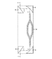
モジュール12、14および16からのネットリスト出力は、また、異なるタイプの要素のそれぞれの物理的レイアウトを実行する構成への別々の入力として提供される。図に示すように、デジタルシミュレーションモジュール12からのネットリスト出力は、「配置配線」レイアウト要素20への入力として与えられ、レイアウト要素20は従来技術においてよく知られている。全カスタムレイアウト要素22を用いて、アナログシミュレーションモジュール14からのネットリスト出力に基づいてアナログ/混合信号構成の物理的レイアウトを取り出す。光学レイアウト要素24は光学レイアウトプロセスを実行し、本発明によれば、次いで3つの「レイアウト」出力が共通検査要素26への入力として提供される。光学レイアウトに関して、従来の設計ルールチェッキング(DRC:Design Rule Checking)を実行して、その設計が所定の工場によって特定されたルールを固守していることを検査する。しかしながら、レイアウト対スケマティックの物理的表示を検査する必要が有る場合(Layout Versus Schematic(LVS)ツールを用いる場合など)に、複雑になる。本発明によれば、検査プロセスに、「確認」層が加えられており、規定された光学要素内の様々なポイントをマークして、構造体内を通過するときの光ビーム路を規定している。図2は、従来のMach-Zehnder干渉計(MZI)構造にこのプロセスを適用した例を示す。図2を参照すると、入力光ビームは、第1の路Aを通って、チューニングミラー30に当たる。次いで、この光ビームは路Bを通り、フォーカッシングミラー32に当たり、このミラーが光ビームを路Cに沿って、MZI34の入力ポートへ再度方向付けをする。MZI34からの出力ビームは、路Dに沿って進み、ここで、出力ミラー36に当たって、光学路E内でフォーカスされる。次いで、この信号がチューニングミラー38によって出力信号路Fへ再度方向付けされる。様々な光学路A−Fの接続性は、従来の集積回路のレイアウトに関連する金属の接続性に例えることができる。従って、この類似性を用いて、上述したように、現存の検査ツールセットによって認識できる光学要素を規定することが可能である。本発明の共通シミュレーションステップを用いたとき、光学的及び電子的要素の双方のレイアウトに関連する様々なパラメータを考慮した共通検査プロセスが用いられる。
The netlist output from
共通の検査プロセスと、共通のシミュレーションプロセスが完了すると、これらのプロセスの結果が比較される。この結果が妥当な合致があれば、完成した設計が所望の通り機能すると推定され、次いで、このプロセスでつくられたデータセットを従来の「テープアウト」に用いて、特定の組立ステップを規定することができる。代替的に、共通検査と共通シミュレーションプロセスの間の結果に違いがある場合は、一又はそれ以上のフィードバック信号を、プロセスを終結させるように変更する必要のある、特定のモジュール/要素に戻す。例えば、特別な光学要素の「レイアウト」は、共通検査プロセスを共通シミュレーションプロセスと合致させるように変更する必要がある場合がある。実際、様々な異なる要素が、ある種の調整を必要とする。更新したネットリスト及び/又はレイアウトが一旦完成すると、共通シミュレーションと、共通検査プロセスが再度実行され、出力が再度比較される。この比較/フィードバックプロセスは、二つの間に予め規定された程度の合致が得られるまで続けられる。 When the common inspection process and the common simulation process are complete, the results of these processes are compared. If this result is a reasonable match, the finished design is presumed to function as desired, and then the data set produced by this process is used for conventional “tape out” to define specific assembly steps. be able to. Alternatively, if there is a difference in the results between the common test and the common simulation process, one or more feedback signals are returned to the specific module / element that needs to be modified to terminate the process. For example, the “layout” of special optical elements may need to be changed to match the common inspection process with the common simulation process. In fact, a variety of different factors require some kind of adjustment. Once the updated netlist and / or layout is completed, the common simulation and common inspection process are performed again and the outputs are compared again. This comparison / feedback process continues until a predefined degree of match is obtained between the two.
図3及び4は、上述したような各タイプの要素を具えるトランスミッタチャネルへ本発明に例示的に適用した共通シミュレーション/共通検査設計プロセスを示す。特に、図3は、例示的なトランスミッタチャネル要素のハイレベルブロック図を示すものであり、図4は、本発明の集積設計法を実行するのに使用することができる例示的プロセスのフローチャートである。図3を参照すると、例示的なトランスミッタチャネル100は、送信が望まれる入力デジタルデータ信号を受信するエンコーダ110を具えるものとして示されている。この分野で知られているように、エンコーダ110は、デジタル入力信号を残りのトランスミッタチャネルに好適に使用した特定のコード化したフォーム(NZRなど)に翻訳する機能がある。エンコーダ110からの出力は、順次、シリアライザ120の入力として与えられ、その後ドライバ130に入れられる。シリアライザ120とドライバ130は、通常、アナログ及びデジタル(混合信号)回路の組み合わせとして用いられる。
3 and 4 illustrate a common simulation / common test design process that is illustratively applied to the present invention to a transmitter channel that includes each type of element as described above. In particular, FIG. 3 shows a high level block diagram of an exemplary transmitter channel element, and FIG. 4 is a flowchart of an exemplary process that can be used to perform the integrated design method of the present invention. . Referring to FIG. 3, an
ドライバ回路120からの出力である、アナログに符号化した情報信号は、次いで、電子−光モジュレータ140への入力として与えられる。別の連続波(CW)光信号が、モジュレータ140への第2の入力として与えられる。この分野でよく知られているように、電気入力信号を用いてCW光信号を変調し、光情報信号を出力として提供する。
The analog encoded information signal that is the output from the
本発明の教示によれば、これらのトランスミッタチャネル要素を全て含む集積構造を展開して、トランスミッタチャネル全体をモノリシック構成として単一のシリコン基板上で実行することが望まれる。図4は、図3に示す集積トランスミッタチャネル100の組立プロセスを生成するのに用いられる方法をハイレベルに示すフローチャートである。図に示すように、このプロセスは、ステップ200で、「デジタル」、「アナログ/混合信号」、「光−電子」として類別することができるハイレベル回路構成における様々な「ブロック」を規定することによって開始する。この特定のケースでは、エンコーダ110が、標準セルを用いて合成することができ、従来の「配置配線」レイアウトプロセスを行う典型的な「デジタル」電子集積回路として規定されている。シリアライザ120とドライバ130は、上述したとおり、A−HDL及び/又はSPICEプロセスを用いて合成することができるデジタル−アナログコンバータ(従って「混合信号」)を含む典型的なアナログ回路として規定される。電子−光モジュレータ140は、電気的入力と光学的入力の両方を用いて光出力信号を形成する、典型的な光−電子要素をとして規定されている。
In accordance with the teachings of the present invention, it is desirable to deploy an integrated structure that includes all of these transmitter channel elements and implement the entire transmitter channel in a monolithic configuration on a single silicon substrate. FIG. 4 is a high-level flowchart illustrating the method used to generate the assembly process for the
様々な要素が規定され、類別されると、各タイプの要素について個別に特定タイプの要素に適したロジック設計プロセスを行う(ステップ210)。すなわち、RTLとシステム設計プロセスをデジタルエンコーダ110に用いて、スタビライザ120とドライバ130のSPICEシミュレーション、および多くの光「標準セル」を規定し、電子「標準セル」とHDLの規定と協働して用いて、電子−光モジュレータ140の変調機能を合成することができる。
Once the various elements are defined and categorized, each type of element is individually subjected to a logic design process appropriate for the particular type of element (step 210). That is, using RTL and system design process for
3つのタイプの要素のロジック設計の完了に続いて、ロジック設計データ(典型的にはネットリストの形、すなわち、コードまたはスケマティックの形のデータ)を共通シミュレーションプロセス220への入力として提供する。本発明によれば、上述したとおり、共通シミュレーションプロセスを用いて、様々なタイプの要素が互いに機能して所望の出力を確実に提供するようにしている。すなわち、各タイプの要素のロジック設計が、単一のシミュレーションプロセス内で互いに融合して、混合信号要素とデジタル要素、さらには、光−電子要素とのデジタル要素の相互作業を査定する。ステップ230に示されるように、別々のロジック設計プロセスからのネットリスト出力は、デジタル要素と、混合信号要素と、光−電子要素の物理的レイアウトを別々に提供するよう機能する物理的レイアウトプロセスへの入力として与えられる。本発明の好ましい実施例では、3つのレイアウトが内部検査プロセスに提供され、共通検査プロセスが開始する前に個別の各レイアウトが正確であることを確認する。
Following completion of the logic design of the three types of elements, logic design data (typically in the form of a netlist, ie code or schematic) is provided as an input to the
この3つの別々の物理的レイアウト構成を規定する(検査済)データは、次いで、ステップ240に示すように共通検査ルーチンへの入力として与えられる。上述したとおり、本発明によって共通検査プロセスが使用され、3つのタイプの要素のレイアウトが正しい態様で互いに動作して、トランスミッタチャネル100の正確な動作を確実にする。共通シミュレーションと共通検査プロセスの双方が完了したら、結果が比較され(ステップ250)、この結果間の合致の度合いに関する決定がなされる(ステップ260)。この結果が十分に合致している場合は、モノリシック構成の完全な設計がなされ、プロセスが「テープアウト」ステージに移る(ステップ270)。
The (inspected) data defining the three separate physical layout configurations is then provided as input to a common inspection routine as shown in
本発明によれば、これらの結果の間に有意な非合致が存在する場合、結果(共通シミュレーション、共通検査のいずれか、あるいは両方)を改善するように変更する特定のプロセス要素に関する決定がなされる(ステップ280)。特定の影響を与える要素が同定されると、訂正/フィードバック信号が入力として与えられ、ロジック設計、物理的レイアウト、あるいはその両方に調整を行うことが可能である。次いで、共通シミュレーションと共通検査プロセスが再び実行され、更新した比較を実行する。このプロセスは、共通のシミュレーションと共通の検査結果の間に十分な合致ができるまで、この方法で続けることができる。 In accordance with the present invention, if there is a significant non-match between these results, a determination is made regarding a particular process element that is modified to improve the results (common simulation, common test, or both). (Step 280). Once a particular influencing element has been identified, a correction / feedback signal is provided as an input and adjustments can be made to the logic design, physical layout, or both. The common simulation and common inspection process is then performed again to perform the updated comparison. This process can continue in this manner until there is a good match between the common simulation and the common test results.
本発明の様々な実行に関する上記記述は、図解と説明の目的でのみ用いられている。これらは、網羅的であり、本発明を開示した形式に限定する意図ではない。従って、当業者には、請求項によって限定される本発明の範囲において、多くの変更と変形が自明である。 The above description of various implementations of the invention is used for illustration and explanation purposes only. These are exhaustive and are not intended to limit the invention to the form disclosed. Accordingly, many modifications and variations will be apparent to practitioners skilled in this art within the scope of this invention as limited by the claims.
図面を参照すると:
Claims (11)
複数の設計モジュールであって、前記複数の設計モジュールの個別モジュールにおいて前記少なくとも一のデジタル要素と、前記少なくとも一のアナログ/混合信号要素と、前記少なくとも一の光−電子要素を、動作/ロジック設計の必要性によって規定し合成する、複数の設計モジュールと;
前記複数の設計モジュールからのロジック設計出力に応じて、各タイプの要素をシミュレートして、同時に前記組み合わせのロジカルな機能を査定する、共通シミュレーションモジュールと;
複数の物理的レイアウトモジュールであって、各々が関連する設計モジュールからのロジック設計出力に応答し、そのロジック設計を物理的レイアウト構成に変換する複数の物理的レイアウトモジュールと;
共通検査モジュールであって、前記複数の物理的レイアウトモジュールからの物理的レイアウト出力に応答し、各タイプの要素の物理的配置と、前記要素の組み合わせの性能の査定を同時に検査する共通検査モジュールと;
共通シミュレーションと共通検査モジュールからの出力に応じて、前記出力間で十分な相関関係に達したかどうかを決定して、最終的なテープアウトを実行するコンパレータと;
を具えることを特徴とする構成。 In a configuration for performing design, layout and inspection of a monolithic integrated circuit structure comprising at least one digital electronic element, at least one analog / mixed signal element, and at least one opto-electronic element:
A plurality of design modules, wherein the at least one digital element, the at least one analog / mixed signal element, and the at least one opto-electronic element in an individual module of the plurality of design modules are operated / logic designed; Multiple design modules, defined and synthesized according to the needs of;
A common simulation module that simulates each type of element according to logic design output from the plurality of design modules and simultaneously assesses the logical function of the combination;
A plurality of physical layout modules, each responding to a logic design output from an associated design module and converting the logic design into a physical layout configuration;
A common inspection module, in response to physical layout output from the plurality of physical layout modules, for simultaneously inspecting the physical placement of each type of element and the assessment of the performance of the combination of elements; ;
A comparator that determines whether a sufficient correlation has been reached between the outputs in response to outputs from the common simulation and common inspection module and performs a final tape-out;
The structure characterized by comprising.
a)統合する設計に含まれるべき要素セットを規定するステップと;
b)デジタル、混合信号、および光−電子の各タイプの要素について別々のロジック設計を作るステップと;
c)前記ロジック設計を全体の設計に組み合わせて、組み合わせたロジック設計の共通シミュレーションを実行するステップと;
d)ステップb)でつくったロジック設計に基づいて、各タイプの要素について別々の物理的レイアウトを生成するステップと;
e)物理的レイアウトを全体の物理的レイアウトと組み合わせて、組み合わせた物理的レイアウトの共通検査を実行するステップと;
f)前記共通シミュレーションの結果を前記共通検査結果と比較するステップと;
g)受け入れ可能である場合は、組立に必要な情報を生成するステップ;さもなければ;
h)変更するべき特定のロジック及び/又は物理的設計を同定するステップと:
i)前記同定した変更を実行するステップと;及び
j)ステップc)と、e)ないしg)を、結果として受け入れ可能な合致が得られるまで繰り返すステップと;
を具えることを特徴とする方法。 In a method for providing integrated design, simulation, and inspection of a monolithic circuit configuration that includes digital electronic elements, mixed signal elements, and opto-electronic elements, the method includes:
a) defining the set of elements to be included in the integrated design;
b) creating separate logic designs for each type of digital, mixed signal, and opto-electronic element;
c) combining the logic design with the overall design and executing a common simulation of the combined logic design;
d) generating a separate physical layout for each type of element based on the logic design created in step b);
e) combining the physical layout with the overall physical layout and performing a common inspection of the combined physical layout;
f) comparing the result of the common simulation with the common test result;
g) if it is acceptable, generating the information necessary for assembly;
h) identifying the specific logic and / or physical design to be changed;
i) performing the identified changes; and j) repeating steps c) and e) to g) until an acceptable match is obtained as a result;
A method characterized by comprising.
Applications Claiming Priority (3)
| Application Number | Priority Date | Filing Date | Title |
|---|---|---|---|
| US58223504P | 2004-06-23 | 2004-06-23 | |
| US11/159,283 US7269809B2 (en) | 2004-06-23 | 2005-06-22 | Integrated approach for design, simulation and verification of monolithic, silicon-based opto-electronic circuits |
| PCT/US2005/022254 WO2006007474A2 (en) | 2004-06-23 | 2005-06-22 | Integrated approach for design, simulation and verification of monolithic, silicon-based opto-electronic circuits |
Publications (2)
| Publication Number | Publication Date |
|---|---|
| JP2008509452A true JP2008509452A (en) | 2008-03-27 |
| JP2008509452A5 JP2008509452A5 (en) | 2008-07-31 |
Family
ID=35507571
Family Applications (1)
| Application Number | Title | Priority Date | Filing Date |
|---|---|---|---|
| JP2007518269A Pending JP2008509452A (en) | 2004-06-23 | 2005-06-22 | An integrated approach for the design, simulation, and inspection of monolithic silicon-based optoelectronic circuits |
Country Status (6)
| Country | Link |
|---|---|
| US (1) | US7269809B2 (en) |
| JP (1) | JP2008509452A (en) |
| KR (1) | KR101145972B1 (en) |
| CN (1) | CN100492372C (en) |
| CA (1) | CA2581451C (en) |
| WO (1) | WO2006007474A2 (en) |
Families Citing this family (30)
| Publication number | Priority date | Publication date | Assignee | Title |
|---|---|---|---|---|
| WO2005054927A2 (en) * | 2003-12-01 | 2005-06-16 | Cdm Optics, Inc. | System and method for optimizing optical and digital system designs |
| US7944467B2 (en) * | 2003-12-01 | 2011-05-17 | Omnivision Technologies, Inc. | Task-based imaging systems |
| US7248757B2 (en) * | 2003-12-15 | 2007-07-24 | Canon Kabushiki Kaisha | Method, device and computer program for designing a circuit having electric wires and optical connections |
| US7672558B2 (en) | 2004-01-12 | 2010-03-02 | Honeywell International, Inc. | Silicon optical device |
| US7149388B2 (en) * | 2004-03-18 | 2006-12-12 | Honeywell International, Inc. | Low loss contact structures for silicon based optical modulators and methods of manufacture |
| US7177489B2 (en) | 2004-03-18 | 2007-02-13 | Honeywell International, Inc. | Silicon-insulator-silicon thin-film structures for optical modulators and methods of manufacture |
| US7217584B2 (en) * | 2004-03-18 | 2007-05-15 | Honeywell International Inc. | Bonded thin-film structures for optical modulators and methods of manufacture |
| US7448012B1 (en) | 2004-04-21 | 2008-11-04 | Qi-De Qian | Methods and system for improving integrated circuit layout |
| US20060063679A1 (en) * | 2004-09-17 | 2006-03-23 | Honeywell International Inc. | Semiconductor-insulator-semiconductor structure for high speed applications |
| CN101288013B (en) * | 2005-09-19 | 2010-12-08 | Cdm光学有限公司 | Task-based imaging system |
| US7362443B2 (en) * | 2005-11-17 | 2008-04-22 | Honeywell International Inc. | Optical gyro with free space resonator and method for sensing inertial rotation rate |
| US7514285B2 (en) * | 2006-01-17 | 2009-04-07 | Honeywell International Inc. | Isolation scheme for reducing film stress in a MEMS device |
| US7442589B2 (en) * | 2006-01-17 | 2008-10-28 | Honeywell International Inc. | System and method for uniform multi-plane silicon oxide layer formation for optical applications |
| US7454102B2 (en) * | 2006-04-26 | 2008-11-18 | Honeywell International Inc. | Optical coupling structure |
| CN100442298C (en) * | 2006-05-15 | 2008-12-10 | 中芯国际集成电路制造(上海)有限公司 | Method for simulating grid root deficiency and MOSFET device performance coherence |
| US8117576B2 (en) * | 2008-03-05 | 2012-02-14 | Rambus Inc. | Method for using an equivalence checker to reduce verification effort in a system having analog blocks |
| US8219947B2 (en) * | 2008-09-15 | 2012-07-10 | Synopsys, Inc. | Method and apparatus for merging EDA coverage logs of coverage data |
| US8316342B1 (en) * | 2010-06-02 | 2012-11-20 | Cadence Design Systems, Inc. | Method and apparatus for concurrent design of modules across different design entry tools targeted to a single layout |
| US8521483B1 (en) | 2010-06-02 | 2013-08-27 | Cadence Design Systems, Inc. | Method and apparatus for concurrent design of modules across different design entry tools targeted to single simulation |
| US8527257B2 (en) | 2011-07-01 | 2013-09-03 | Fujitsu Limited | Transition-based macro-models for analog simulation |
| US8903698B2 (en) | 2012-05-15 | 2014-12-02 | Fujitsu Limited | Generating behavioral models for analog circuits |
| US20150067621A1 (en) * | 2012-09-05 | 2015-03-05 | Mentor Graphics Corporation | Logic-Driven Layout Pattern Analysis |
| CN103164566A (en) * | 2012-12-04 | 2013-06-19 | 天津蓝海微科技有限公司 | Vector testing auxiliary layer generating method of territory validation rule |
| US8856701B1 (en) * | 2013-03-12 | 2014-10-07 | Taiwan Semiconductor Manufacturing Co., Ltd. | Method of radio-frequency and microwave device generation |
| US8726205B1 (en) | 2013-04-15 | 2014-05-13 | Nvidia Corporation | Optimized simulation technique for design verification of an electronic circuit |
| US8813019B1 (en) | 2013-04-30 | 2014-08-19 | Nvidia Corporation | Optimized design verification of an electronic circuit |
| CN105653744A (en) * | 2014-11-13 | 2016-06-08 | 中芯国际集成电路制造(上海)有限公司 | Method and device for designing layout |
| US10650110B2 (en) | 2015-07-08 | 2020-05-12 | Hewlett Packard Enterprise Development Lp | Photonic circuit design systems |
| US11023648B2 (en) | 2017-12-12 | 2021-06-01 | Siemens Industry Software Inc. | Puzzle-based pattern analysis and classification |
| CN117332742B (en) * | 2023-12-01 | 2024-02-23 | 芯动微电子科技(武汉)有限公司 | Simulation verification method and device for chip design stage |
Citations (3)
| Publication number | Priority date | Publication date | Assignee | Title |
|---|---|---|---|---|
| JP2001230638A (en) * | 2000-02-18 | 2001-08-24 | Nec Eng Ltd | Method for designing optical transmitting circuit and optical receiving circuit |
| JP2005174154A (en) * | 2003-12-15 | 2005-06-30 | Canon Inc | Method, device and program for designing circuit having electric wiring and optical connection |
| JP2005174153A (en) * | 2003-12-15 | 2005-06-30 | Canon Inc | Method, device and program for designing circuit having electric wiring and optical connection |
Family Cites Families (28)
| Publication number | Priority date | Publication date | Assignee | Title |
|---|---|---|---|---|
| US5544067A (en) * | 1990-04-06 | 1996-08-06 | Lsi Logic Corporation | Method and system for creating, deriving and validating structural description of electronic system from higher level, behavior-oriented description, including interactive schematic design and simulation |
| US5222030A (en) * | 1990-04-06 | 1993-06-22 | Lsi Logic Corporation | Methodology for deriving executable low-level structural descriptions and valid physical implementations of circuits and systems from high-level semantic specifications and descriptions thereof |
| US5930150A (en) * | 1996-09-06 | 1999-07-27 | Lucent Technologies Inc. | Method and system for designing and analyzing optical application specific integrated circuits |
| US5914889A (en) * | 1996-09-13 | 1999-06-22 | Lucent Technologies Inc. | Method and system for generating a mask layout of an optical integrated circuit |
| US6110217A (en) * | 1997-10-03 | 2000-08-29 | International Business Machines Corporation | System and method for synchronization of multiple analog servers on a simulation backplane |
| US6845184B1 (en) * | 1998-10-09 | 2005-01-18 | Fujitsu Limited | Multi-layer opto-electronic substrates with electrical and optical interconnections and methods for making |
| US7031889B1 (en) * | 1999-03-22 | 2006-04-18 | Hewlett-Packard Development Company, L.P. | Method and apparatus for evaluating the design quality of network nodes |
| US6446243B1 (en) * | 1999-04-23 | 2002-09-03 | Novas Software, Inc. | Method for functional verification of VLSI circuit designs utilizing reusable functional blocks or intellectual property cores |
| US6438735B1 (en) * | 1999-05-17 | 2002-08-20 | Synplicity, Inc. | Methods and apparatuses for designing integrated circuits |
| US6480816B1 (en) * | 1999-06-14 | 2002-11-12 | Sanjay Dhar | Circuit simulation using dynamic partitioning and on-demand evaluation |
| US6816825B1 (en) * | 1999-06-18 | 2004-11-09 | Nec Corporation | Simulation vector generation from HDL descriptions for observability-enhanced statement coverage |
| US7065481B2 (en) * | 1999-11-30 | 2006-06-20 | Synplicity, Inc. | Method and system for debugging an electronic system using instrumentation circuitry and a logic analyzer |
| US6587995B1 (en) * | 2000-04-19 | 2003-07-01 | Koninklijke Philips Electronics N.V. | Enhanced programmable core model with integrated graphical debugging functionality |
| US6718522B1 (en) * | 2000-08-15 | 2004-04-06 | Hewlett-Packard Development Company, L.P. | Electrical rules checker system and method using tri-state logic for electrical rule checks |
| US6502223B1 (en) * | 2001-04-30 | 2002-12-31 | Hewlett-Packard Company | Method for simulating noise on the input of a static gate and determining noise on the output |
| US6912330B2 (en) * | 2001-05-17 | 2005-06-28 | Sioptical Inc. | Integrated optical/electronic circuits and associated methods of simultaneous generation thereof |
| US6980945B2 (en) * | 2001-12-04 | 2005-12-27 | Koninklijke Philips Electronics N.V. | Synchronized simulation of software and hardware in the analog domain |
| US6745372B2 (en) * | 2002-04-05 | 2004-06-01 | Numerical Technologies, Inc. | Method and apparatus for facilitating process-compliant layout optimization |
| US20030195736A1 (en) * | 2002-04-11 | 2003-10-16 | Sun Microsystems, Inc. | Method of storing cross-hierarchy coupling data in a hierarchical circuit model |
| US6898767B2 (en) * | 2002-05-09 | 2005-05-24 | Lsi Logic Corporation | Method and apparatus for custom design in a standard cell design environment |
| US6826739B2 (en) * | 2002-05-13 | 2004-11-30 | Agilent Technologies, Inc. | System and method for placing substrate contacts in a datapath stack in an integrated circuit design |
| US6983443B2 (en) * | 2002-05-22 | 2006-01-03 | Agilent Technologies, Inc. | System and method for placing clock drivers in a standard cell block |
| US6807658B2 (en) * | 2002-06-05 | 2004-10-19 | Agilent Technologies, Inc. | Systems and methods for performing clock gating checks |
| US6815729B1 (en) * | 2002-10-09 | 2004-11-09 | Cypress Semiconductor Corp. | Electro-optical apparatus |
| AU2002952700A0 (en) * | 2002-11-18 | 2002-11-28 | Vpisystems Pty Ltd | Simulation player |
| US7055113B2 (en) * | 2002-12-31 | 2006-05-30 | Lsi Logic Corporation | Simplified process to design integrated circuits |
| US7155689B2 (en) * | 2003-10-07 | 2006-12-26 | Magma Design Automation, Inc. | Design-manufacturing interface via a unified model |
| US6969903B2 (en) * | 2004-01-19 | 2005-11-29 | International Business Machines Corporation | High tolerance TCR balanced high current resistor for RF CMOS and RF SiGe BiCMOS applications and cadenced based hierarchical parameterized cell design kit with tunable TCR and ESD resistor ballasting feature |
-
2005
- 2005-06-22 US US11/159,283 patent/US7269809B2/en active Active
- 2005-06-22 CA CA2581451A patent/CA2581451C/en not_active Expired - Fee Related
- 2005-06-22 CN CNB200580020911XA patent/CN100492372C/en not_active Expired - Fee Related
- 2005-06-22 WO PCT/US2005/022254 patent/WO2006007474A2/en active Application Filing
- 2005-06-22 JP JP2007518269A patent/JP2008509452A/en active Pending
- 2005-06-22 KR KR1020077001314A patent/KR101145972B1/en active IP Right Grant
Patent Citations (3)
| Publication number | Priority date | Publication date | Assignee | Title |
|---|---|---|---|---|
| JP2001230638A (en) * | 2000-02-18 | 2001-08-24 | Nec Eng Ltd | Method for designing optical transmitting circuit and optical receiving circuit |
| JP2005174154A (en) * | 2003-12-15 | 2005-06-30 | Canon Inc | Method, device and program for designing circuit having electric wiring and optical connection |
| JP2005174153A (en) * | 2003-12-15 | 2005-06-30 | Canon Inc | Method, device and program for designing circuit having electric wiring and optical connection |
Also Published As
| Publication number | Publication date |
|---|---|
| US20050289490A1 (en) | 2005-12-29 |
| CA2581451C (en) | 2013-09-24 |
| CN101036145A (en) | 2007-09-12 |
| WO2006007474A2 (en) | 2006-01-19 |
| CN100492372C (en) | 2009-05-27 |
| US7269809B2 (en) | 2007-09-11 |
| KR101145972B1 (en) | 2012-05-22 |
| WO2006007474A3 (en) | 2007-04-19 |
| CA2581451A1 (en) | 2006-01-19 |
| KR20070040792A (en) | 2007-04-17 |
Similar Documents
| Publication | Publication Date | Title |
|---|---|---|
| US7269809B2 (en) | Integrated approach for design, simulation and verification of monolithic, silicon-based opto-electronic circuits | |
| Riesgo et al. | Design methodologies based on hardware description languages | |
| US7937256B2 (en) | Systems and methods of efficient library characterization for integrated circuit cell libraries | |
| JPH10207937A (en) | Method and device for executing verification after layout of micro electronics circuit by filtering timing error limit value for layout critical network and computer program product | |
| US8205177B2 (en) | Non-linear receiver model for gate-level delay calculation | |
| KR20090077692A (en) | Semiconductor-device manufacturing method, semiconductor-device manufacturing program and semiconductor-device manufacturing system | |
| KR100749753B1 (en) | Simulation method and apparatus at gate level, method of desiging ics, method of designing ics including voltage islands, and method of designing chips | |
| US20040025136A1 (en) | Method for designing a custom ASIC library | |
| Sadrossadat et al. | Nonlinear electronic/photonic component modeling using adjoint state-space dynamic neural network technique | |
| López et al. | Reuse-based methodologies and tools in the design of analog and mixed-signal integrated circuits | |
| US6560571B1 (en) | Method and apparatus for prioritizing the order in which checks are performed on a node in an integrated circuit | |
| US6550041B1 (en) | Method and apparatus for evaluating the design quality of network nodes | |
| US6449578B1 (en) | Method and apparatus for determining the RC delays of a network of an integrated circuit | |
| Heins et al. | Design flow automation for silicon photonics: Challenges, collaboration, and standardization | |
| US7086017B1 (en) | Method of post-implementation simulation of a HDL design | |
| US6732343B2 (en) | System and methods for placing clock buffers in a datapath stack | |
| US8316336B1 (en) | Method and mechanism for modeling interconnect structures for integrated circuits | |
| US6718522B1 (en) | Electrical rules checker system and method using tri-state logic for electrical rule checks | |
| Lienig et al. | Methodologies for Physical Design: Models, Styles, Tasks, and Flows | |
| US6484295B1 (en) | Electrical rules checker system and method providing quality assurance of tri-state logic | |
| US11334704B1 (en) | System, method, and computer program product for mixed signal verification | |
| Kundert et al. | Analog verification | |
| Richard | Building a System | |
| Llamas et al. | Development of digital application specific printed electronics circuits: from specification to final prototypes | |
| JP2006031277A (en) | Method for generating verification vector, and method for verifying electronic circuit by using the same |
Legal Events
| Date | Code | Title | Description |
|---|---|---|---|
| A521 | Written amendment |
Free format text: JAPANESE INTERMEDIATE CODE: A523 Effective date: 20080610 |
|
| A621 | Written request for application examination |
Free format text: JAPANESE INTERMEDIATE CODE: A621 Effective date: 20080610 |
|
| A131 | Notification of reasons for refusal |
Free format text: JAPANESE INTERMEDIATE CODE: A131 Effective date: 20100511 |
|
| A02 | Decision of refusal |
Free format text: JAPANESE INTERMEDIATE CODE: A02 Effective date: 20101019 |