JP2008287528A - Request arbitration device and memory controller - Google Patents
Request arbitration device and memory controller Download PDFInfo
- Publication number
- JP2008287528A JP2008287528A JP2007132245A JP2007132245A JP2008287528A JP 2008287528 A JP2008287528 A JP 2008287528A JP 2007132245 A JP2007132245 A JP 2007132245A JP 2007132245 A JP2007132245 A JP 2007132245A JP 2008287528 A JP2008287528 A JP 2008287528A
- Authority
- JP
- Japan
- Prior art keywords
- bank
- request
- access
- requests
- lru
- Prior art date
- Legal status (The legal status is an assumption and is not a legal conclusion. Google has not performed a legal analysis and makes no representation as to the accuracy of the status listed.)
- Pending
Links
Images


Classifications
-
- G—PHYSICS
- G06—COMPUTING; CALCULATING OR COUNTING
- G06F—ELECTRIC DIGITAL DATA PROCESSING
- G06F12/00—Accessing, addressing or allocating within memory systems or architectures
- G06F12/02—Addressing or allocation; Relocation
- G06F12/06—Addressing a physical block of locations, e.g. base addressing, module addressing, memory dedication
-
- G—PHYSICS
- G06—COMPUTING; CALCULATING OR COUNTING
- G06F—ELECTRIC DIGITAL DATA PROCESSING
- G06F13/00—Interconnection of, or transfer of information or other signals between, memories, input/output devices or central processing units
- G06F13/14—Handling requests for interconnection or transfer
- G06F13/16—Handling requests for interconnection or transfer for access to memory bus
- G06F13/1605—Handling requests for interconnection or transfer for access to memory bus based on arbitration
- G06F13/161—Handling requests for interconnection or transfer for access to memory bus based on arbitration with latency improvement
- G06F13/1626—Handling requests for interconnection or transfer for access to memory bus based on arbitration with latency improvement by reordering requests
- G06F13/1631—Handling requests for interconnection or transfer for access to memory bus based on arbitration with latency improvement by reordering requests through address comparison
Landscapes
- Engineering & Computer Science (AREA)
- Theoretical Computer Science (AREA)
- Physics & Mathematics (AREA)
- General Engineering & Computer Science (AREA)
- General Physics & Mathematics (AREA)
- Bus Control (AREA)
- Memory System (AREA)
Abstract
Description
この発明は、複数のイニシエータからの所定のメモリに対するアクセス等のリクエストを調停するバスアービタ等のリクエスト調停装置及びメモリコントローラに関する。 The present invention relates to a request arbitration device such as a bus arbiter that arbitrates requests such as access to a predetermined memory from a plurality of initiators, and a memory controller.
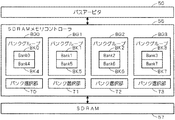
図15は従来のバスアービタとその周辺部とのシステム構成を示すブロック図である。同図に示すように、バスアービタ64はCPU60及びイニシエータ61〜63とSDRAMメモリコントローラ65との間に設けられる。
FIG. 15 is a block diagram showing a system configuration of a conventional bus arbiter and its peripheral part. As shown in the figure, the
バスアービタ64はCPU60及びイニシエータ61〜63からのリクエストを調停し、SDRAMメモリコントローラ65へリクエストを発行する。イニシエータ61〜63それぞれは画像系(2D,3D)や画像圧縮、音声などの多量のデータ転送を必要としている。このため、バスアービタ64ではイニシエータ61〜63それぞれからの要求を満たせるようにアービトレーション(調停)を行う必要がある。
The
イニシエータ61〜63それぞれからバスアービタ64へは、SDRAM(Synchronous Dynamic Random Access Memory)66に関し異なるアドレスに対するリクエストが発行される。そこで、バスアービタ64にてSDRAM66のアクセス時におけるページミス、バンクミスや他のイニシエータによる割り込みによるペナルティが少なくなるようにアービトレーションを行うことにより、SDRAM66に対するコマンド発行効率を向上させることが必要となる。なお、上述したペナルティとして、例えば、バンクミスペナルティ、ページミスペナルティ等が挙げられる。
Requests for different addresses regarding SDRAM (Synchronous Dynamic Random Access Memory) 66 are issued from each of the
SDRAM66に対するコマンド発行の効率を上げるため、バスアービタ64にてSDRAM66のバンクヒット/ミス、SDRAM66への先行PRE,ACTコマンド発行などを考慮に入れたアービトレーションを行う。
In order to increase the efficiency of command issuance to the
なお、SDRAM66に対するコマンド発行の効率を上げたメモリアクセス要求の調停技術として例えば特許文献1に開示された技術がある。特許文献1では最終アクセスページと同一のページにアクセス要求するメモリマスタに優先的にアクセス許可を与えている調停技術が開示されている。
As a memory access request arbitration technique that increases the efficiency of issuing commands to the
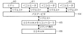
図16はSDRAMメモリコントローラ65及びその周辺を示すブロック図である。一般にSDRAMメモリコントローラ65では8バンクSDRAMのアクセス効率向上方式を採用している。
FIG. 16 is a block diagram showing the
SDRAMメモリコントローラ65はバスアービタ64からのリクエストを受けてSDRAM66に対してコマンドを発行する。
The SDRAM
また、DDR2(Double-Data-Rate2)-SDRAM等を含むSDRAMでは4,8バンク品のSDRAMが存在する。8バンク品を用いた場合にSDRAMメモリコントローラでは、8バンク品の制御方式は4バンクまでをオープンするようにしているが、5個目のバンクをオープンするときにクローズするバンクは、対となる決められたバンクである。 In addition, SDRAMs including DDR2 (Double-Data-Rate2) -SDRAM and the like include SDRAMs of 4 or 8 banks. When an 8-bank product is used, in the SDRAM memory controller, the control system for the 8-bank product is configured to open up to 4 banks, but the bank that is closed when the fifth bank is opened is paired. It is a fixed bank.
バスアービタでは各イニシエータの処理データが破綻しない待ち時間を考慮する必要がある。イニシエータが破綻しない待ち時間を「許容時間」とする。イニシエータのデータ破綻とは、グラフィックス系のイニシエータでは画像が乱れること、音声系のイニシエータでは音声が途切れたりすることを指す。 In the bus arbiter, it is necessary to consider a waiting time during which the processing data of each initiator does not fail. The waiting time at which the initiator does not fail is defined as “allowable time”. The data failure of the initiator means that the image is disturbed in the graphics type initiator, and the sound is interrupted in the audio type initiator.
しかしながら、従来のバスアービタや特許文献1で開示されたメモリアクセス要求の調停技術では、上記許容時間を考慮したリクエスト調停を行っていないという問題点があった。
However, the conventional bus arbiter and the memory access request arbitration technique disclosed in
また、上記した8バンク品の制御方式では、上記許容時間を全く考慮していない点は勿論、5個目のバンクをオープンするときにクローズするバンクは、対となる決められたバンクであるため、アクセスされやすいバンクをクローズしてしまう可能性があった。このため、SDRAMアクセス性能低下が起こるといった問題点があった。 Further, in the control system for the 8-bank product described above, the allowable bank is not taken into account at all, and the bank that is closed when the fifth bank is opened is a bank that is determined as a pair. There was a possibility of closing the bank that was easily accessed. For this reason, there has been a problem that SDRAM access performance is reduced.
この発明は上記問題点を解決するためになされたもので、イニシエータが破綻しない待ち時間である許容時間を考慮し、かつ、効率的なリクエスト調停が行えるリクエスト調停装置及び制御対象のメモリの性能向上を図ったメモリコントローラ得ることを目的とする。 The present invention has been made to solve the above-described problems, and considers an allowable time that is a waiting time for which an initiator does not fail, and improves the performance of a request arbitration device that can efficiently perform request arbitration and a memory to be controlled. An object is to obtain a memory controller that achieves the above.
この発明の一実施の形態によれば、許容時間判定機能付きページヒットミス判定部は、互いに連動して動作するページミスヒット判定部及び許容時間判定部を有している。 According to one embodiment of the present invention, the page hit / miss determination unit with an allowable time determination function includes a page miss / hit determination unit and an allowable time determination unit that operate in conjunction with each other.
ページミスヒット判定部は、複数のリクエストそれぞれのSDRAMへのアクセスアドレスと前回アクセスアドレスとを比較する。そして、互いのアドレスが指定するバンク及びページが一致するページヒットの有無を前記複数のリクエストそれぞれについて判定し、複数のリクエストのうち、ページヒットしたリクエストの中から優先的に優先リクエストとして決定する。 The page miss hit determination unit compares the access address to the SDRAM of each of the plurality of requests with the previous access address. Then, the presence / absence of a page hit corresponding to the bank and page specified by each other's address is determined for each of the plurality of requests, and the priority request is determined preferentially from among the requests having a page hit.
許容時間判定部は、複数のイニシエータに対応して設定された複数の許容時間の残存時間が所定時間以下に達したイニシエータである要メモリアクセスイニシエータが存在した場合、複数のリクエストのうち、要メモリアクセスイニシエータのリクエストを、ページヒットミス判定部の決定より優先させて優先リクエストして決定可能な構成を呈している。 When there is a memory access initiator that is an initiator whose remaining time of a plurality of allowable times set corresponding to the plurality of initiators has reached a predetermined time or less, the allowable time determination unit includes The configuration is such that the request of the access initiator can be determined by giving a priority request over the determination of the page hit / miss determination unit.
この実施の形態によれば、ページヒット判定部及び許容時間判定部の連携により、ページヒットしたリクエストを優先することによりSDRAMに対するリクエストの発行効率が向上する効果を得ながら、許容時間判定部によって各イニシエータの許容時間を優先考慮したリクエスト調整を行うことができる。 According to this embodiment, by the cooperation of the page hit determination unit and the allowable time determination unit, each of the allowable time determination units obtains the effect of improving the request issuing efficiency to the SDRAM by giving priority to the page hit request. It is possible to perform request adjustment in consideration of the allowable time of the initiator.
<前提技術>
(バスアービトレーション方式)
図12はこの発明の前提技術となるバスアービトレーション方式を示すブロック図である。同図に示すように、バスアービタ50は(n+1)個(n≧1)のイニシエータINI0〜INInからのSDRAMに対するリクエストRQ0〜RQnのアービトレーション(調停)を行う。なお、以下ではリクエストRQ0〜RQnのいずれかを指す場合、単にリクエストRQと称する場合がある。
<Prerequisite technology>
(Bus arbitration method)
FIG. 12 is a block diagram showing a bus arbitration system which is a prerequisite technology of the present invention. As shown in the figure, the
まず、リクエストRQ0〜RQnはバンクヒットミス判定部51にてアービトレーションが行われる。バンクヒットミス判定部51では前回にSDRAMメモリコントローラ55に送られたリクエストの前回転送アドレスADpとイニシエータINI0〜INInの現在のアドレス情報AD0〜ADnを保持している。
First, the requests RQ0 to RQn are arbitrated by the bank hit /
そして、バンクヒットミス判定部51は前回転送アドレスADpとアドレス情報AD0〜ADnとを比較して、前回送られたリクエストと異なるバンクアドレス(バンクミス)のアドレスを指定したリクエストを認識し、リクエストRQ0〜RQnのうち、前回転送アドレスADpと異なるバンクアドレス(バンク)のリクエストを優先し、許容時間アービタ52の処理対象とする。一方、リクエストRQ0〜RQnのうち、前回転送アドレスADpと同じバンクアドレス(バンク)のリクエストは優先度が下げられて、許容時間アービタ53の処理対象とする。
Then, the bank hit /
以下、リクエストRQ0〜RQnのうち、バンクヒットミス判定部51でバンクミスと判定されたリクエストをバンクミスリクエストMRQとし、バンクヒットリクエストHRQとして説明する。
Hereinafter, of the requests RQ0 to RQn, a request determined as a bank miss by the bank hit
許容時間アービタ52,53では、イニシエータINI0〜INInそれぞれの処理データが破綻しない待ち時間である許容時間をレジスタ(図示せず)にて設定する。具体的には、各イニシエータがリクエストを発行してからイニシエータにレスポンスが帰って来るまでのサイクル数を満たせることが可能な時間が許容時間となる。
In the
この許容時間を上記レジスタにて設定することによりシステムごとにアービトレーションを変更でき、イニシエータごとの使用可能な時間の割り振りを細かく設定することが可能となる。すなわち、許容時間アービタ52,53では、イニシエータINI0〜INInそれぞれの許容時間を設定してアービトレーションを行う。
By setting this allowable time in the register, arbitration can be changed for each system, and the allocation of usable time for each initiator can be set in detail. That is, the
許容時間アービタ52,53は許容時間を用いたアービトレーションを行うために、イニシエータごと許容時間をカウントするための許容時間カウンタPCA0〜PCAn,許容時間カウンタPCB0〜PCBnをそれぞれ有する。これら許容時間カウンタPCA0〜PCAn及び許容時間カウンタPCB0〜PCBnはイニシエータINI0〜INInに対応して設けられる。なお、許容時間カウンタPCA0〜PCAn及び許容時間カウンタPCB0〜PCBnのいずれかを示す場合、単に許容時間カウンタPCA及び許容時間カウンタPCBと称す場合がある。
The
許容時間カウンタPCA0〜PCAn及び許容時間カウンタPCB0〜PCBnはそれぞれ、対応するイニシエータのリクエストをメモリコントローラ55へ送っていない場合に許容時間カウント値をダウンカウントし、対応するイニシエータのリクエストをメモリコントローラ55に送った場合には対応する上記レジスタに設定した時間だけ許容時間をプラスする。
The permissible time counters PCA0 to PCAn and permissible time counters PCB0 to PCBn down-count the permissible time count value when the corresponding initiator request is not sent to the
許容時間カウンタPCA0〜PCAn及び許容時間カウンタPCB0〜PCBnそれぞれの上記レジスタに設定する値は任意であるため、イニシエータINI0〜INInに対するアービトレーションのチューニングが可能となる。カウント値CTのレベル閾値(カウント閾値LVth)を定め、許容時間カウンタのカウント値CTがカウント閾値LVthより小さくなったイニシエータのリクエストRQを最優先する。この場合、当該リクエストRQがバンクミスリクエストMRQであるかバンクヒットリクエストHRQであるかに関係なく、緊急処理として優先リクエストPRQ10(優先リクエストPRQ11,PRQ12)がSDRAMメモリコントローラ55に送られる。
Since the values set in the registers of the permissible time counters PCA0 to PCAn and permissible time counters PCB0 to PCBn are arbitrary, it is possible to tune arbitration for the initiators INI0 to INIn. A level threshold value (count threshold value LVth) of the count value CT is determined, and the request RQ of the initiator whose count value CT of the allowable time counter is smaller than the count threshold value LVth is given the highest priority. In this case, regardless of whether the request RQ is a bank miss request MRQ or a bank hit request HRQ, a priority request PRQ10 (priority requests PRQ11, PRQ12) is sent to the
例えば、バンクミスリクエストMRQが少なくとも一つが存在する場合、許容時間アービタ52による処理が実行される。しかし、許容時間カウンタPCA0〜PCAnのカウント値CTのうち、一つでもカウント閾値LVthを下回るが存在すれば、カウント値判定部58によって、当該カウント値CTに対応するイニシエータのリクエストRQである許容時間低下リクエストERQが最優先に優先リクエストPRQ10とされる。この場合、許容時間低下リクエストERQがバンクミスリクエストMRQであるか否かは関係なく優先される。
For example, when at least one bank miss request MRQ exists, processing by the
一方、許容時間カウンタPCA0〜PCAn(許容時間カウンタPCB0〜PCBn)のカウント値CTが全てカウント閾値LVthより大きい場合は通常のアービトレーションが許容時間アービタ52,53によって実行される。以下、許容時間アービタ52,53の通常処理について説明する。
On the other hand, when the count values CT of the allowable time counters PCA0 to PCAn (allowable time counters PCB0 to PCBn) are all greater than the count threshold LVth, normal arbitration is executed by the
許容時間アービタ52の対象となるバンクミスリクエストMRQが複数存在する場合、カウント値判定部58は、複数のバンクミスリクエストMRQに対応する複数の許容時間カウンタPCAのカウント値CTのうち、最も小さいカウント値CTに対応するバンクミスリクエストMRQを優先リクエストPRQ11として選択する。
When there are a plurality of bank miss requests MRQ that are targets of the
一方、許容時間アービタ52の対象となるバンクミスリクエストMRQが存在しない場合、バンクヒットリクエストHRQの中から許容時間アービタ53が優先リクエストPRQ12を選択する。許容時間アービタ53内のカウント値判定部59は、対象となるバンクヒットリクエストHRQのうち最も小さいカウント値CTに対応するバンクヒットリクエストHRQを優先リクエストPRQ12として選択する。
On the other hand, when there is no bank miss request MRQ targeted for the
なお、許容時間アービタ53によるアービトレーション実行時に、許容時間カウンタPCB0〜PCBnのカウント値CTのうち、一つでもカウント閾値LVthを下回るがカウント値CTが存在すれば、カウント値判定部59によって、当該カウント値CTに対応するリクエストRQである許容時間低下リクエストERQが最優先に優先リクエストPRQ12とされる。
When arbitration is performed by the
図13はある許容時間カウンタPCA(PCB)のカウント動作例を示す説明図である。同図に示すように、カウント値CTは対応するリクエスト実発行の際、予め設定された許容時間分プラスされる。なお、リクエスト実発行とはカウント値CTに対応するイニシエータから出力されたリクエストがバスアービタ50によって優先リクエストPRQ11(PRQ12)として決定され、SDRAMメモリコントローラ55からSDRAMに実際に出力されたことを意味する。一方、リクエスト無発行時はクロックサイクル(サイクル数CCL)の経過と伴にカウントダウンされる。図13に示すように、タイミングt1,t2時にはカウント閾値LVthを下回ったため、最優先処理され必ずリクエストが発行される。
FIG. 13 is an explanatory diagram showing a count operation example of a certain allowable time counter PCA (PCB). As shown in the figure, the count value CT is incremented by a preset allowable time when the corresponding request is issued. The request actual issue means that the request output from the initiator corresponding to the count value CT is determined as the priority request PRQ11 (PRQ12) by the
(SDRAMメモリコントローラ)
図14はSDRAMメモリコントローラ55の詳細を示す説明図である。SDRAMメモリコントローラ55は対象となるSDRAM57が8バンク品(バンクBK0〜BK7)の場合の構成を示している。
(SDRAM memory controller)
FIG. 14 is an explanatory diagram showing details of the
同図に示すように、SDRAMメモリコントローラ55は4つのバンクグループBG0〜BG3によって、SDRAM57における8バンクのオープン/クローズ制御を行っている。すなわち、バンクグループBG0はバンクBK0及びバンクBK4をペアとし、バンク選択部70によって一方をオープン,他方をクローズしている。同様にして、バンクグループBG1はバンクBK1及びバンクBK5をペアとし、バンク選択部71によって一方をオープン,他方をクローズしている。バンクグループBG2はバンクBK2及びバンクBK6をペアとし、バンク選択部72によって一方をオープン,他方をクローズしている。バンクグループBG3はバンクBK3及びバンクBK7をペアとし、バンク選択部73によって一方をオープン,他方をクローズしている。
As shown in the figure, the
このように、前提技術となるSDRAMメモリコントローラ55は、バンクグループBG0〜BG3で規定されるバンクの組合せを一対としてバンクグループBG0〜BG3それぞれにおいて一方のバンクのみバンクオープンする仕様としていた。したがって、5バンク目のバンクアクセス要求がバスアービタ50により行われた場合は、バンクグループBG0〜BG3のうち、5バンク目にオープンするバンクと対となる他方のバンクが強制的にクローズされていた。
As described above, the
(前提技術の問題点)
図12及び図13で示した前提技術となるバスアービトレーション方式では、通常処理においては、バンクミスしたリクエストを優先してメモリコントローラへ送っていた。アドレスに関するアービトレーションがバンクアドレスのヒットミス判定のみである。
(Problems of the base technology)
In the bus arbitration method as the prerequisite technology shown in FIGS. 12 and 13, in the normal processing, the bank missed request is preferentially sent to the memory controller. Arbitration related to the address is only hit / miss determination of the bank address.
しかしながら、バンクミス及びページミスした場合は、SDRAM57に対するアクセス時に必ず信号PRE,ACTを発行するため、SDRAM57に十分な性能を発揮させることができないという問題点があった。
However, if a bank miss or page miss occurs, the signals PRE and ACT are always issued when the
図14で示したSDRAMメモリコントローラのバンク切替方式の場合、8バンク品の5バンク目をオープンにするときにクローズするバンクアドレスは性能に依存してクローズするわけではない。このため、本来はバンクヒットするため信号PRE,ACTを発行しなくても良い場合にでも、バンクがクローズされてしまっている場合は信号PRE,ACTを発行しなければならないため、SDRAMへのコマンド発行効率が低下する。 In the case of the SDRAM memory controller bank switching method shown in FIG. 14, the bank address that is closed when the fifth bank of the 8-bank product is opened does not depend on the performance. For this reason, even if it is not necessary to issue the signals PRE and ACT because the bank hits originally, the signal PRE and ACT must be issued if the bank is closed. Issuing efficiency decreases.
上述した問題点の解消を図り、本願発明のリクエスト調停装置であるバスアービタは、SDRAMのコマンド発行順を最適にする事で転送効率を向上させ、かつ許容時間を考慮することを可能にしている。また、本願発明のメモリコントローラは、SDRAMの性能向上を図ることができる。 In order to solve the above-described problems, the bus arbiter, which is a request arbitration device according to the present invention, can improve the transfer efficiency by optimizing the SDRAM command issuance order and can consider the allowable time. Further, the memory controller of the present invention can improve the performance of the SDRAM.
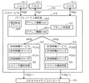
<実施の形態1>
図1はこの発明の実施の形態1であるリクエスト調停装置であるバスアービタの構成を示すブロック図である。同図に示すように、実施の形態1のバスアービタ1は、イニシエータINI0〜INIn(図示せず)のリクエストRQ0〜RQnを受ける。バスアービタ1は、内部に許容時間判定機能付きページヒットミス判定部2、許容時間判定機能付きバンクオープンクローズ判定部3、及び許容時間判定機能付きLRU部4を有している。
<
1 is a block diagram showing a configuration of a bus arbiter which is a request arbitration apparatus according to
同図に示すように、リクエスト調停の優先順位はページヒット、バンクオープン、LRU(Least Recently Used(最も遅く使用されていたバンク))の順で、SDRAMに対するバンク優先順位が決定する。さらに、各判定部2〜4は内部に許容時間判定部22,32,42を有しており、後に詳述するように、判定部2〜4の優先処理においても、許容時間がカウント閾値LVthを下回ったイニシエータのリクエストRQを最優先処理する。
As shown in the figure, the priority order of request arbitration is determined in the order of page hit, bank open, and LRU (Least Recently Used) in the order of bank priority. Further, each of the
なお、実施の形態1のバスアービタ1は、アクセス対象となる所定のメモリであるSDRAMは、複数のバンクが割り当てられており、複数のバンクはそれぞれ複数のページ(通常、行アドレスによって割当)が割り当てられていることを前提としている。
In the
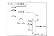
図2はバスアービタ1における許容時間判定機能付きページヒットミス判定部2の内部構成を示すブロック図である。同図に示すように、許容時間判定機能付きページヒットミス判定部2はページミスヒット判定部21及び許容時間判定部22を有している。
FIG. 2 is a block diagram showing an internal configuration of the page hit /
ページミスヒット判定部21は前回転送アドレス情報保持部PAIS、アドレス情報保持部AIS0〜AISnを有している。前回転送アドレス情報保持部PAISは、直前にメモリコントローラ10に与えた優先リクエストPRQにおける前回転送アドレスADp(前回アクセスアドレス)を保持している。アドレス情報保持部AIS0〜AISnはイニシエータINI0〜INInから現在発行されているリクエストRQ0〜RQnにおけるSDRAMへのアクセスアドレスをアドレス情報AD0〜ADnとして保持している。
The page miss hit
図3はページミスヒット判定部21の内部構成の内部構成を示す説明図である。なお、図2と図3とを合わせた構成がページミスヒット判定部21の内部構成となる。
FIG. 3 is an explanatory diagram showing the internal configuration of the internal configuration of the page miss hit
比較回路23は前回転送アドレス情報保持部PAISから得られる前回転送アドレスADpと、アドレス情報保持部AIS0〜AISnから得られるアドレス情報AD0〜ADnと、許容時間判定部22の許容時間カウンタPC0〜PCnから得られるカウント値CT0〜CTnとを受ける。そして、比較回路23は前回転送アドレスADpとアドレス情報AD0〜ADnとのバンクアドレス及びページアドレスを比較して、アドレス情報AD0〜ADnそれぞれのページヒットの有無を判定する。その結果、比較回路23はアドレス情報AD0〜ADnのうちページヒットしたアドレスであるページヒットアドレスHADを認識する。
The comparison circuit 23 uses the previous transfer address ADp obtained from the previous transfer address information holding unit PAIS, the address information AD0 to ADn obtained from the address information holding units AIS0 to AISn, and the allowable time counters PC0 to PCn of the allowable
さらに、比較回路23は、ページヒットアドレスHADが複数存在する場合は、カウント値CT0〜CTnからページヒットアドレスHADそれぞれに対応するカウント値CTを比較し、カウント値CTが最も小さいページヒットアドレスHADを優先ページヒットアドレスPHADとする。そして、比較回路23は、イニシエータINI0〜INInのうち、優先ページヒットアドレスPHADを含むリクエストRQを発行したイニシエータを優先イニシエータとして指示する優先イニシエータ情報PIJ1を出力する。 Further, when there are a plurality of page hit addresses HAD, the comparison circuit 23 compares the count values CT corresponding to the page hit addresses HAD from the count values CT0 to CTn, and selects the page hit address HAD having the smallest count value CT. The priority page hit address PHAD is used. Then, the comparison circuit 23 outputs priority initiator information PIJ1 that instructs the initiator that has issued the request RQ including the priority page hit address PHAD among the initiators INI0 to INIn as the priority initiator.
セレクタ24は、後述する優先イニシエータ情報PIJ2が要メモリアクセスイニシエータ無しを指示する場合、リクエストRQ0〜RQnのうち優先イニシエータ情報PIJ1の指示するイニシエータに対応するリクエストRQを優先リクエストPRQ2として選択する。
When the priority initiator information PIJ2 to be described later indicates no memory access initiator required, the
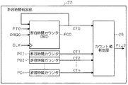
図4は許容時間判定部22の内部構成の詳細を示すブロック図である。同図に示すように、許容時間判定部22は許容時間カウンタPC0〜PCn及びカウント値判定部25から構成される。許容時間カウンタPC0〜PCnはイニシエータINI0〜INInに対応して設けられる。
FIG. 4 is a block diagram showing details of the internal configuration of the allowable
許容時間カウンタPC0はリクエスト実発行情報ORQ0、許容時間情報PT0、及びクロックCLKを受け、カウント値CT0を出力する。なお、リクエスト実発行情報ORQ0とは対応のリクエストRQ0が優先リクエストPRQとして実際にメモリコントローラ10に発行された場合に活性状態となる情報である。許容時間情報PTは図示しないレジスタ等の記憶部にイニシエータINI0〜INInそれぞれに対応して格納されている許容時間を指示する情報である。
The allowable time counter PC0 receives the request actual issue information ORQ0, the allowable time information PT0, and the clock CLK, and outputs a count value CT0. The request actual issue information ORQ0 is information that is activated when the corresponding request RQ0 is actually issued to the
許容時間カウンタPC0はクロックCLKに同期してカウント値CT0をカウントダウンする。この際、リクエスト実発行情報ORQ0が活性状態になると、許容時間情報PT0で指示された許容時間をカウント値CT0にプラスする。 The allowable time counter PC0 counts down the count value CT0 in synchronization with the clock CLK. At this time, when the request actual issue information ORQ0 becomes active, the allowable time indicated by the allowable time information PT0 is added to the count value CT0.
なお、許容時間カウンタPC1〜PCnも許容時間カウンタPC0と同様、対応するリクエスト実発行情報ORQ、許容時間情報PTと共に、クロックCLKを受け、カウント値CT1〜CTnを出力している。 As with the allowable time counter PC0, the allowable time counters PC1 to PCn receive the clock CLK together with the corresponding request actual issue information ORQ and the allowable time information PT, and output the count values CT1 to CTn.
このように、許容時間カウンタPC0〜PCnでカウントされるカウント値CT0〜CTnは、イニシエータINI0〜INInの許容時間の残存時間を意味する。したがって、許容時間を考慮した場合、カウント値CTi(i=1〜nのいずれか)の小さいイニシエータINIiのリクエストRQiを優先的に処理する方が望ましい。 As described above, the count values CT0 to CTn counted by the allowable time counters PC0 to PCn mean the remaining time of the allowable time of the initiators INI0 to INIn. Therefore, when the allowable time is taken into consideration, it is desirable to preferentially process the request RQi of the initiator INIi having a small count value CTi (i = 1 to n).
カウント値判定部25はカウント値CT0〜CTnを受け、カウント値CT0〜CTnとカウント閾値LVthとを比較して、カウント閾値LVthを下回るカウント値CTが存在する場合、当該カウント値CTに対応するイニシエータである要メモリアクセスイニシエータを指示する優先イニシエータ情報PIJ2を出力する。
The count
一方、カウント値判定部25は、カウント閾値LVthを下回るカウント値CTが存在しない場合は、要メモリアクセスイニシエータ無しを指示する優先イニシエータ情報PIJ2を出力する。
On the other hand, when there is no count value CT that is lower than the count threshold LVth, the count
図3に戻って、セレクタ24は優先イニシエータ情報PIJ2をさらに受け、優先イニシエータ情報PIJ2が指示する要メモリアクセスイニシエータが存在する場合は、優先イニシエータ情報PIJ1の指示内容に関係なく、優先イニシエータ情報PIJ2の指示する要メモリアクセスイニシエータのリクエストRQを最優先して優先リクエストPRQ2として選択する。
Returning to FIG. 3, the
このように、実施の形態1のバスアービタ1の許容時間判定機能付きページヒットミス判定部2は、互いに連動して動作するページミスヒット判定部21及び許容時間判定部22を有している。
Thus, the page hit /
ページミスヒット判定部21は、リクエストRQ0〜RQnのうちページヒットしたリクエストの中から優先的に優先リクエストPRQ2を決定する。許容時間判定部22は、イニシエータINI0〜INInの許容時間の残存時間であるカウント値CT0〜CTnがカウント閾値LVth以下に達した要メモリアクセスイニシエータのリクエストを、ページミスヒット判定部21の決定(優先イニシエータ情報PIJ1の指示内容)より優先して優先リクエストPRQ2として決定させることができる。
The page miss hit
したがって、実施の形態1のバスアービタ1は、ページヒットしたリクエストを優先することによりSDRAMに対するコマンド(優先リクエスト)の発行効率が向上する効果を得ながら、イニシエータINI0〜INInそれぞれの許容時間を優先考慮したリクエスト調停を行うことができる。
Therefore, the
また、実施の形態1のバスアービタ1のページミスヒット判定部21における比較回路23は、ページヒットしたリクエストが複数存在した場合、ページヒットしたリクエストに対応するイニシエータのうち、カウント値CT0〜CTnに基づき許容時間の残存時間がより小さいイニシエータを指示する優先イニシエータ情報PIJ1をセレクタ24に出力している。すなわち、ページミスヒット判定部21の比較回路23及びセレクタ24によって、ページヒットしたリクエストが複数存在した場合、許容時間の残存時間がより小さいリクエストを優先的に優先リクエストPRQ2として決定するページヒット優先処理機能を実現している。
The comparison circuit 23 in the page miss hit
したがって、優先イニシエータ情報PIJ2による要メモリアクセスイニシエータの指示がない場合に実行されるページヒット優先処理時においてもイニシエータINI0〜INInの許容時間を考慮したリクエスト調停が行える。 Therefore, even when page hit priority processing is executed when there is no instruction of the memory access initiator required by the priority initiator information PIJ2, request arbitration taking into account the allowable time of the initiators INI0 to INIn can be performed.
図5はバスアービタ1における許容時間判定機能付きバンクオープンクローズ判定部3の内部構成を示すブロック図である。同図に示すように、許容時間判定機能付きバンクオープンクローズ判定部3はバンクオープンクローズ判定部31及び許容時間判定部32を有している。許容時間判定機能付きバンクオープンクローズ判定部3は、許容時間判定機能付きページヒットミス判定部2によってページヒットしたリクエストが存在しなかった場合に起動する。
FIG. 5 is a block diagram showing an internal configuration of the bank open /
バンクオープンクローズ判定部31はイニシエータINI0〜INInに対応してバンクオープンクローズ判定部BOC0〜BOCnを有している。バンクオープンクローズ判定部BOC0〜BOCnはリクエストRQ0〜RQnのアクセス対象のバンクが現在オープンしているか否かのオープン/クローズ判定を行う。
The bank open / close determining
図6はバンクオープンクローズ判定部31の内部構成の詳細を示す説明図である。同図に示すように、バンクオープンクローズ判定部BOC0〜BOCnはリクエストRQ0〜RQnを受け、共通にSDRAMアドレスSDADを受ける。なお、SDRAMアドレスSDADはSDRAMにアクセスした際のアドレスを意味する。なお、バンクオープンクローズ判定部BOC0〜BOCnに取り込まれたSDRAMアドレスSDADはフリップフロップFF0〜FFnを介して過去履歴格納部AS0〜ASn内に過去履歴情報として所定量蓄積される。すなわち、過去履歴格納部AS0〜ASnにはそれぞれ過去のSDRAMアドレスSDADの履歴が過去履歴情報として格納される。
FIG. 6 is an explanatory diagram showing details of the internal configuration of the bank open / close determining
バンクオープンクローズ判定部BOCi(i=0〜nのいずれか)はリクエストRQiと過去履歴格納部ASiの過去履歴情報を参照して、リクエストRQiの指示するSDRAMへのアクセスバンクがオープン状態であるかクローズ状態であるを判定し、オープン・クローズ判定結果ROCiを出力する。 The bank open / close determining unit BOCi (i = 0 to n) refers to the request RQi and the past history information of the past history storage unit ASi, and determines whether the access bank to the SDRAM indicated by the request RQi is open. The closed state is determined, and the open / close determination result ROCi is output.
なお、許容時間判定部32の構成及び動作は許容時間判定機能付きページヒットミス判定部2内の許容時間判定部22と同様であるため説明を省略する。なお、許容時間判定部32の許容時間カウンタPCX0〜PCXnが許容時間カウンタPC0〜PCnに対応すし、許容時間カウンタPCX0〜PCXnのカウント値CT0〜CTn及び優先イニシエータ情報PIJ2をセレクタ33に出力する。なお、カウント値CT0〜CTn及び優先イニシエータ情報PIJ2の内容は許容時間判定部22と同様である。
The configuration and operation of the allowable time determination unit 32 are the same as those of the allowable
セレクタ33はオープン・クローズ判定結果ROC0〜ROCnと共に、許容時間判定部32から得られるカウント値CT0〜CTn及び優先イニシエータ情報PIJ2を受ける。
The
そして、セレクタ33は、優先イニシエータ情報PIJ2が要メモリアクセスイニシエータを指示しない場合、オープン・クローズ判定結果ROC0〜ROCn及びカウント値CT0〜CTnに基づき、バンクオープン状態を指示するリクエストRQのうちカウント値CTが最も小さいものをリクエストRQ0〜RQnから抽出して、優先リクエストPRQ3として選択する。
Then, when the priority initiator information PIJ2 does not indicate a memory access initiator that is required, the
一方、セレクタ33は、優先イニシエータ情報PIJ2が要メモリアクセスイニシエータを指示する場合、リクエストRQ0〜RQnのうち、優先イニシエータ情報PIJ2の指示するリクエストRQを最優先に優先リクエストPRQ3として選択する。
On the other hand, when the priority initiator information PIJ2 indicates a memory access initiator that is required, the
このように、実施の形態1のバスアービタ1における許容時間判定機能付きバンクオープンクローズ判定部3は、互いに連動して動作するバンクオープンクローズ判定部31及び許容時間判定部32を有している。
As described above, the bank open /
バンクオープンクローズ判定部31は、各リクエストについてバンクオープンの有無を判定した情報をオープン・クローズ判定結果ROC0〜ROCnとして出力する。許容時間判定部22は、要メモリアクセスイニシエータを指示する優先イニシエータ情報PIJ2をセレクタ33に与える。
The bank open / close determining
セレクタ33は、優先イニシエータ情報PIJ2が要メモリアクセスイニシエータを指示する場合、バンクオープンクローズ判定部31の決定(オープン・クローズ判定結果ROCi)より優先イニシエータ情報PIJ2の指示する要メモリアクセスイニシエータのリクエストを優先して優先リクエストPRQ3して決定する。
When the priority initiator information PIJ2 indicates a memory access initiator that is required, the
一方、セレクタ33は、優先イニシエータ情報PIJ2が要メモリアクセスイニシエータを指示しない場合、バンクオープンクローズ判定部31の決定(オープン・クローズ判定結果ROCi)に基づき優先リクエストPRQ3を決定する。
On the other hand, when the priority initiator information PIJ2 does not indicate a memory access initiator that is required, the
したがって、SDRAMにおけるバンクのオープンクローズ状態を考慮することによりSDRAMに対するコマンド発行効率の向上を図りながら、イニシエータINI0〜INInそれぞれの許容時間を優先的に考慮したリクエスト調停を行うことができる。 Therefore, it is possible to perform request arbitration in consideration of the allowable time of each of the initiators INI0 to INIn while improving the command issue efficiency to the SDRAM by considering the open / close state of the bank in the SDRAM.
また、実施の形態1のバスアービタ1のセレクタ33は、バンクオープンと判定したリクエストが複数存在した場合、カウント値CT0〜CTnに基づき許容時間の残存時間がより小さいイニシエータのリクエストを優先的に優先リクエストPRQ3として決定する。すなわち、許容時間判定機能付きバンクオープンクローズ判定部3は、バンクオープンクローズ判定部31及びセレクタ33によって、ページヒットしたリクエストが複数存在した場合、許容時間の残存時間がより小さいリクエストを優先的に優先リクエストPRQ3として決定するバンクオープン優先処理機能を有している。
Further, the
このため、優先イニシエータ情報PIJ2が要メモリアクセスイニシエータを指示しない場合に実行されるバンクオープン優先処理時においても複数のイニシエータの許容時間を優先考慮したリクエスト調停が行える。 For this reason, even in the bank open priority process that is executed when the priority initiator information PIJ2 does not indicate a memory access initiator that is required, request arbitration can be performed in consideration of the allowable times of a plurality of initiators.
図7はバスアービタ1における許容時間判定機能付きLRU部4の内部構成を示すブロック図である。同図に示すように、許容時間判定機能付きLRU部4はLRU判定部41及び許容時間判定部42を有している。許容時間判定機能付きLRU部4は許容時間判定機能付きバンクオープンクローズ判定部3によってバンクオープンと判定したリクエストが存在しなかった場合に起動する。
FIG. 7 is a block diagram showing an internal configuration of the
図8はLRU判定部41の内部構成の詳細を示す説明図である。同図において、過去履歴情報格納部45は過去のSDRAMアドレスSDADに基づき、SDRAMに対するバンクアクセス履歴情報を格納している。LRUステートマシン43はリクエストRQ0〜RQn及び過去履歴情報格納部45からのバンクアクセス履歴情報I45を受ける。そして、LRUステートマシン43は、バンクアクセス履歴情報I45によって最新アクセス時間が最も古いLRUバンク、すなわち、最も以前にアクセスされたLRUバンクを認識し、当該LRUバンクにバンクアクセスするリクエストRQを指示する情報をLRUリクエスト情報RQLとしてセレクタ44に出力する。
FIG. 8 is an explanatory diagram showing details of the internal configuration of the
なお、許容時間判定部42の構成及び動作は許容時間判定機能付きページヒットミス判定部2内の許容時間判定部22と同様であるため説明を省略する。また、許容時間判定部42の許容時間カウンタPCY0〜PCYnが許容時間カウンタPC0〜PCnに対応すし、許容時間カウンタPCY0〜PCYnのカウント値CT0〜CTn及び優先イニシエータ情報PIJ2をセレクタ44に出力する。なお、カウント値CT0〜CTn及び優先イニシエータ情報PIJ2の内容は許容時間判定部22の場合と同様である。
The configuration and operation of the allowable
セレクタ44はリクエストRQ0〜RQn及びLRUリクエスト情報RQLと共に、許容時間判定部42から得られるカウント値CT0〜CTn及び優先イニシエータ情報PIJ2を受ける。
The
そして、セレクタ44は、優先イニシエータ情報PIJ2が優先イニシエータを指示しない場合、LRUリクエスト情報RQLに基づき、LRUバンクにアクセスするリクエストのうち、カウント値CTが最も小さいリクエストRQをリクエストRQ0〜RQnから抽出して、優先リクエストPRQ4として選択する。
Then, when the priority initiator information PIJ2 does not indicate a priority initiator, the
一方、セレクタ44は、優先イニシエータ情報PIJ2が優先イニシエータを指示する場合、LRUリクエスト情報RQLの内容に関係なく、リクエストRQ0〜RQnのうち、優先イニシエータ情報PIJ2の指示するリクエストRQを最優先に優先リクエストPRQ4として選択する。
On the other hand, when the priority initiator information PIJ2 indicates the priority initiator, the
また、セレクタ44は、優先イニシエータ情報PIJ2が優先イニシエータを指示せず、LRUバンクにアクセスするリクエストが存在しない場合、単純にカウント値CT0〜CTnの最小のリクエストRQをリクエストRQ0〜RQnから抽出して、優先リクエストPRQ4として選択する(単純許容時間低下優先処理)。
Further, when the priority initiator information PIJ2 does not indicate the priority initiator and there is no request for accessing the LRU bank, the
このように、実施の形態1のバスアービタ1における許容時間判定機能付きLRU部4は、互いに連動するLRU判定部41及び許容時間判定部42を有している。
As described above, the
LRU判定部41は最新アクセス時間が最も古いLRUバンクをアクセスバンクとするリクエストを指示するLRUリクエスト情報RQLを出力する。許容時間判定部42は要メモリアクセスイニシエータを指示する優先イニシエータ情報PIJ2を出力する。LRU判定部41内のセレクタ44は、優先イニシエータ情報PIJ2が要メモリアクセスイニシエータを指示する場合、LRU判定部41の決定(LRUリクエスト情報RQLの指示内容)より優先して要メモリアクセスイニシエータのリクエストを優先リクエストPRQ4として出力する。
The
一方、優先イニシエータ情報PIJ2が要メモリアクセスイニシエータを指示しない場合、LRU判定部41の決定(LRUリクエスト情報RQL)に従い、LRUバンクにアクセスするリクエストを優先的に選択して優先リクエストPRQ4を出力する。 On the other hand, when the priority initiator information PIJ2 does not indicate a memory access initiator that is required, according to the determination of the LRU determination unit 41 (LRU request information RQL), a request to access the LRU bank is preferentially selected and a priority request PRQ4 is output.
したがって、実施の形態1のバスアービタ1の許容時間判定機能付きLRU部4は、SDRAMのLRUバンクをオープンさせてアクセスすることにより、SDRAMに対するコマンド発行効率の向上を図りながら、イニシエータINI0〜INInそれぞれの許容時間を優先的に考慮したリクエスト調停を行うことができる。
Therefore, the
バスアービタ1の許容時間判定機能付きLRU部4のLRU判定部41内のセレクタ44は、LRUリクエスト情報RQLが複数のLRUバンクを指示する場合、カウント値CT0〜CTnに基づき許容時間の残存時間がより小さいリクエストを優先的に優先リクエストPRQ4と決定している。すなわち、LRU判定部41はLRUステートマシン43及びセレクタ44によって、LRUバンクへのバンクアクセスするリクエストが複数存在した場合、許容時間の残存時間がより小さいリクエストを優先的に優先リクエストPRQ4として決定するLRUバンク優先処理機能を有している。
When the LRU request information RQL indicates a plurality of LRU banks, the
したがって、実施の形態1のバスアービタ1は、カウント値CT0〜CTnを考慮したLRUバンク優先処理機能によって、LRUバンク優先処理時においても複数のイニシエータの許容時間を考慮したリクエスト調停が行える。
Therefore, the
図9は図1〜図8で示した実施の形態1のバスアービタ1のバスアービトレーション方式の処理手順を示すフローチャートである。以下、同図を参照して、実施の形態1のバスアービタ1によるバスアービトレーション方式の処理手順を説明する。
FIG. 9 is a flowchart showing a processing procedure of the bus arbitration method of the
まず、ステップS1によって、許容時間判定機能付きページヒットミス判定部2により、全ての許容時間判定用のカウント値CT0〜CTnがカウント閾値LVth以上であるか否かを判定する。
First, in step S1, the page hit
ステップS1において、カウント閾値LVth以上と判定するとステップS2に移行し、カウント値CT0〜CTnのうち少なくとも一つにおいてカウント閾値LVth以下と判定するとステップS15の許容時間低下最優先処理を行う。 If it is determined in step S1 that the count threshold LVth is greater than or equal to step S2, the process proceeds to step S2. If at least one of the count values CT0 to CTn is determined to be less than or equal to the count threshold LVth, the allowable time reduction highest priority process in step S15 is performed.
ステップS1からステップS15に至る処理が、図4で示した許容時間判定部22から優先イニシエータを指示する優先イニシエータ情報PIJ2が出力された場合、ページミスヒット判定部21のセレクタ24によって、優先イニシエータ情報PIJ2の指示するイニシエータのリクエストRQをリクエストRQ0〜RQnから抽出し、優先リクエストPRQ2として選択する処理に相当する。
In the processing from step S1 to step S15, when the priority initiator information PIJ2 instructing the priority initiator is output from the allowable
ステップS2において、リクエストRQ0〜RQnすべてについてページヒットの有無を判定する。すなわち、リクエストRQ0〜RQnのうち少なくとも一つのリクエストRQでページヒットであると判定すると、ステップS11のページヒット優先処理を行い、全リクエストRQ0〜RQnがページミスであると判定するとステップS3に移行する。 In step S2, the presence or absence of a page hit is determined for all requests RQ0 to RQn. That is, when it is determined that at least one request RQ among the requests RQ0 to RQn is a page hit, the page hit priority process of step S11 is performed, and when it is determined that all the requests RQ0 to RQn are a page miss, the process proceeds to step S3. .
ステップS2からステップS11に至る処理が、図3で示したページミスヒット判定部21内のセレクタ24によって、優先イニシエータ情報PIJ1及びカウント値CT0〜CTnに基づき、優先リクエストPRQ2として選択するページヒット優先処理に相当する。
The processing from step S2 to step S11 is the page hit priority processing selected as the priority request PRQ2 based on the priority initiator information PIJ1 and the count values CT0 to CTn by the
ステップS3において、許容時間判定機能付きバンクオープンクローズ判定部3により、全ての許容時間判定用のカウント値CT0〜CTnがカウント閾値LVth以上であるか否かを判定する。
In step S3, the bank open /
ステップS3において、全てのカウント値CT0〜CTnがカウント閾値LVth以上と判定するとステップS4に移行し、少なくとも一つのカウント値CTiがカウント閾値LVth以下であると判定するとステップS15の許容時間低下最優先処理を行う。 If it is determined in step S3 that all the count values CT0 to CTn are equal to or greater than the count threshold LVth, the process proceeds to step S4. If it is determined that at least one count value CTi is equal to or less than the count threshold LVth, the allowable time reduction highest priority process in step S15 is performed. I do.
ステップS3からステップS15に至る処理が、図5で示した許容時間判定部32から優先イニシエータを指示する優先イニシエータ情報PIJ2が出力された場合、セレクタ33によって、優先イニシエータ情報PIJ2の指示するイニシエータのリクエストRQをリクエストRQ0〜RQnから抽出し、優先リクエストPRQ3として選択する処理に相当する。
In the process from step S3 to step S15, when the priority initiator information PIJ2 indicating the priority initiator is output from the allowable time determination unit 32 shown in FIG. 5, the
ステップS4において、全てのリクエストRQ0〜RQnに対しバンクオープンの有無を判定し、リクエストRQ0〜RQnのうち少なくとも一つのリクエストRQでアクセス対象のバンクがオープン状態であると判定すると、ステップS12のバンクオープン優先処理を行い、全リクエストRQ0〜RQnでアクセス対象のバンクがクローズである判定するとステップS5に移行する。 In step S4, it is determined whether or not a bank is open for all requests RQ0 to RQn, and if it is determined that the access target bank is open in at least one request RQ among the requests RQ0 to RQn, the bank open in step S12 is performed. If priority processing is performed and it is determined that the access target bank is closed in all requests RQ0 to RQn, the process proceeds to step S5.
ステップS4からステップS12に至る処理が、図5,図6で示したバンクオープンクローズ判定部31内のセレクタ33によって、オープン・クローズ判定結果ROC0〜ROCn及びカウント値CT0〜CTnに基づき、リクエストRQ0〜RQnから優先リクエストPRQ3を選択するバンクオープン優先処理に相当する。
The processing from step S4 to step S12 is performed by the
ステップS5において、許容時間判定機能付きLRU部4により、全ての許容時間判定用のカウント値CT0〜CTnがカウント閾値LVth以上であるか否かを判定する。
In step S5, the
ステップS5において、カウント値CT0〜CTnが全てカウント閾値LVth以上と判定するとステップS6に移行し、少なくとも一つがカウント閾値LVth以下と判定するとステップS15の許容時間低下最優先処理を行う。 In step S5, if all the count values CT0 to CTn are determined to be equal to or greater than the count threshold LVth, the process proceeds to step S6. If at least one is determined to be equal to or less than the count threshold LVth, the allowable time reduction top priority process in step S15 is performed.
ステップS5からステップS15に至る処理が、図7で示した許容時間判定部42から優先イニシエータを指示する優先イニシエータ情報PIJ2が出力された場合、セレクタ44によって、優先イニシエータ情報PIJ2の指示するイニシエータのリクエストRQをリクエストRQ0〜RQnから抽出し、優先リクエストPRQ4として選択する処理に相当する。
In the processing from step S5 to step S15, when the priority initiator information PIJ2 indicating the priority initiator is output from the allowable
ステップ6において、LRU判定を行う。すなわち、リクエストRQ0〜RQnのうち少なくとも一つのリクエストRQが最も使用されていないバンク(最新アクセス時間が最も古いバンク)にアクセスするリクエストであるか否かを判定する。そして、LRU判定を満足した(LRUバンクである)と判定すると、ステップS13のLRUバンク優先処理を行い、全リクエストRQ0〜RQnでLRU判定を満足しないと判定するとステップS14の単純許容時間低下優先処理を実行する。 In step 6, LRU determination is performed. That is, it is determined whether at least one request RQ among the requests RQ0 to RQn is a request for accessing a bank that is least used (the bank having the oldest latest access time). If it is determined that the LRU determination is satisfied (is an LRU bank), the LRU bank priority process in step S13 is performed. If it is determined that the LRU determination is not satisfied for all requests RQ0 to RQn, the simple allowable time reduction priority process in step S14 is performed. Execute.
ステップS6からステップS13に至る処理が、図8で示したLRU判定部41内のセレクタ44が、優先イニシエータ情報PIJ2が優先イニシエータを指示しない場合、LRUリクエスト情報RQLに基づき、LRUバンクにアクセスするリクエストのうち、カウント値CTが最も小さいリクエストRQをリクエストRQ0〜RQnから抽出して、優先リクエストPRQ4として選択する処理に相当する。
The processing from step S6 to step S13 is a request for accessing the LRU bank based on the LRU request information RQL when the
一方、ステップS6からステップS14に至る処理が、図8で示したLRU判定部41内のセレクタ44によって、優先イニシエータ情報PIJ2が優先イニシエータを指示せず、LRUバンクにアクセスするリクエストが存在しない場合、単純にカウント値CT0〜CTnの最小のリクエストRQをリクエストRQ0〜RQnから抽出して、優先リクエストPRQ4として選択する処理に相当する。
On the other hand, if the processing from step S6 to step S14 is not performed by the
図17は実施の形態1のバスアービタの他の態様のバスアービトレーション方式の処理手順を示すフローチャートである。同図に示すように、ステップS3及びステップS5の処理を省略している。ステップS3およびステップS5は、ステップS1と同内容の処理の繰り返しであるため、図17に示すフローのように、ステップS3及びステップS5の処理を省略することができる。すなわち、ステップS2でミス判定した後にステップS4の判定を実行し、ステップS4でクローズ判定した後にステップS6を判定するフローでも良い。 FIG. 17 is a flowchart showing the processing procedure of the bus arbitration method of another aspect of the bus arbiter of the first embodiment. As shown in the figure, the processing of step S3 and step S5 is omitted. Since step S3 and step S5 are repetitions of the same process as step S1, the process of step S3 and step S5 can be omitted as in the flow shown in FIG. In other words, a flow may be used in which the determination in step S4 is executed after making a mistake determination in step S2, and the determination in step S6 is made after the close determination in step S4.
図18は図17のフローに対応する実施の形態1の他の態様であるバスアービタ1sのハードウェア構成を示すブロック図である。同図に示すように、図1で示したバスアービタ1に対し、図18で示したバスアービタ1sは、許容時間判定機能付きバンクオープンクローズ判定部3を単純バンクオープンクローズ判定部3sに、許容時間判定機能付きLRU部4を単純LRU部4sに置き換えている点が異なる。単純バンクオープンクローズ判定部3sはバンクオープンクローズ判定部31を内部に有し、許容時間判定部32に相当する構成部を省略している。同様にして、単純LRU部4sはLRU判定部41を内部に有し許容時間判定部42に相当する構成部を省略している。
FIG. 18 is a block diagram showing a hardware configuration of a bus arbiter 1s which is another aspect of the first embodiment corresponding to the flow of FIG. As shown in the figure, the bus arbiter 1s shown in FIG. 18 is different from the
さらに、図18に示すバスアービタ1sは、許容時間判定部22の許容時間カウンタPC0〜PCnから出力されるカウント値CT0〜CTnを、単純バンクオープンクローズ判定部3s及び単純LRU部4sに入力する構成を呈している。なお、単純LRU部4sは単純バンクオープンクローズ判定部3s経由でカウント値CT0〜CTnを入力している。
Furthermore, the bus arbiter 1s shown in FIG. 18 is configured to input the count values CT0 to CTn output from the allowable time counters PC0 to PCn of the allowable
すなわち、許容時間判定部22で得られたカウント値CT0〜CTnをバンクオープンクローズ判定部31およびLRU部41においても活用している。その結果、図18で示したバスアービタ1sにおいても、ステップS12のバンクオープン優先処理、ステップS13のLRUバンク優先処理、及びステップS14の許容時間低下優先処理を支障無く行うことができる。
That is, the count values CT0 to CTn obtained by the allowable
<実施の形態2>
図10はこの発明の実施の形態2であるメモリコントローラ10の構成を示す説明図である。実施の形態2のメモリコントローラ10は実施の形態1のバスアービタ1に対応し、バスアービタ1より得られる優先リクエストPRQ(PRQ2〜PRQ4のいずれか)に基づき制御対象となるSDRAMに対しアクセスする。
<
FIG. 10 is an explanatory diagram showing the configuration of the
なお、メモリコントローラ10は制御対象となるSDRAMが8バンク構成の場合を前提としている。すなわち、制御対象なるSDRAMは8バンクを有し、うち4バンク(所定数=4)をオープンできる構成を前提としている。
The
図10に示すように、メモリコントローラ10は内部に8バンク制御部11を有し、8バンク制御部11はLRUモジュール12及びバンク切替部13を備えている。8バンク制御部11は優先リクエストPRQがクローズしているバンクにアクセスするリクエストである場合に、オープン状態の所定数のバンクのいずかをクローズするバンククローズ制御を行う。
As shown in FIG. 10, the
図11は8バンク制御部11の詳細を示す説明図である。同図に示すように、優先リクエストPRQはLRUモジュール12及びバンク切替部13に入力される。
FIG. 11 is an explanatory diagram showing details of the 8-
LRUモジュール12はLRU状態保持部15内に制御対象のSDRAMにおける各バンクの最新アクセス時間を指示するLRUバンク情報I15を格納している。そして、LRUモジュール12は、LRU状態保持部15に格納したLRUバンク情報I15をバンク切替部13に出力する。LRUモジュール12はメモリコントローラ10からSDRAMに発行されるSDRAMアドレスSDAD(図示せず)に基づき、制御対象のSDRAMにおける各バンクの最新アクセス時間を常時更新し、LRUバンク情報I15としてLRU状態保持部15内に保持している。
The
バンク切替部13はLRUバンク情報I15、現在、オープンしているバンクのうち、最新アクセス時間が最も古いLRUオープンバンクを認識し、当該LRUオープンバンクをクローズし、優先リクエストPRQの指示するバンクをオープンするバンク切替制御を制御対象のSDRAMに対して行う。
The
実施の形態2のメモリコントローラ10は、オープン許容数を超える5バンク目のバンクをオープンにするためにはいずれかのバンクをクローズする際、SDRAMへのアクセスを向上させるため、LRUバンク情報I15に基づきLRUオープンバンクをクローズさせている。すなわち、メモリコントローラ10は、アクセス時間の古い順にクローズするというクローズバンクの優先順位を決めてバンク切替制御をSDRAMに対して行っている。
The
このように、実施の形態2のメモリコントローラ10におけるバンク切替部13は、4個のバンクのいずれかをクローズする際、LRU状態保持部15からのLRUバンク情報I15に基づき、4個のバンクのうち最新アクセス時間が最も古いLRUオープンバンクを優先的にクローズするバンク切替を行っている。
As described above, the
LRUオープンバンクは使用頻度が低いと推測されるバンクであるため、実施の形態2のメモリコントローラ10は、LRUオープンバンクを優先的にクローズすることにより、使用頻度が高いバンクがオープン状態となる確率が高くなるため、SDRAMの性能向上を図ることができる効果を奏する。
Since the LRU open bank is a bank that is presumed to be used infrequently, the
また、図14で示したSDRAMメモリコントローラ55と比較した場合、バンクグループBG0〜BG3によるオープンバンクとクローズバンクとが対となる制約がないマルチ制御が行うことができる。その結果、オープンすべきバンクに制約がない分、先行コマンド処理が実行できるため、SDRAMの転送効率を考慮したコマンドをSDRAMに発行することができる。
Further, when compared with the
なお、実施の形態2の第1の変形例として、イニシエータからのアクセスを予め考慮し、常時オープンにするバンクを決める態様も考えられる。この場合、予め決定された常時オープンバンクに対し、バンク切替部13はクローズせず常時オープン状態となるように制御する。
Note that, as a first modification of the second embodiment, a mode in which an access from an initiator is considered in advance and a bank that is always open can be considered. In this case, the
その結果、予め使用頻度が高いことが認識されている常時オープンバンクへのアクセス効率が向上し、全体としてのアクセス効率が向上する効果が得られる。 As a result, it is possible to improve the access efficiency to the always-open bank, which is recognized to be frequently used in advance, and to improve the access efficiency as a whole.
なお、常時オープンバンクをハードウェア固定にする態様も考えられる。例えば、図11に示すように、バンク切替部13はオープン固定バンク設定情報14を有し、オープン固定バンク設定情報14で指定されたバンクは常にオープンするように制御するようにしても良い。この場合、オープン固定バンク設定情報14の指示するバンクを常時オープンにしながら、他のオープンバンク内においてLRUオープンバンクをクローズ制御する常時バンクオープン制御を行うことになる。
A mode in which the open bank is always fixed to hardware is also conceivable. For example, as shown in FIG. 11, the
このように、実施の形態2の第1の変形例では、バンク切替部13は、オープン固定バンク設定情報14に従い4個のバンクのうち一部をオープン固定バンクとして常時オープン状態にする常時オープン制御を実行する。したがって、常時オープンするバンクを使用頻度の高いバンクに設定することにより、バンクミスペナルティを少なくして所定のメモリに対するリクエストの発行効率を向上させることができる効果を奏する。
As described above, in the first modification of the second embodiment, the
さらに、実施の形態2の第2の変形例として、常時オープンバンクを設定するか否かを指示する指示レジスタ16を8バンク制御部11内に設け、指示レジスタ16内の指示内容に基づき、オープンバンク固定の採用の有無を決定しても良い。すなわち、バンク切替部13は、指示レジスタ16の指示内容に基づき、全バンクに対してLRUバンクをクローズ制御する全LRU制御を行うか、上記常時バンクオープン制御を行うかを切り替えることができる。
Further, as a second modification of the second embodiment, an
このように、実施の形態2の第2の変形例では、バンク切替部13は、指示レジスタ16の指示内容に基づき、上記常時オープン制御を行うか否かを切り換える機能を有することにより、状況に応じて常時オープン制御の利用の有無を使い分けることができる。
As described above, in the second modification of the second embodiment, the
<その他>
実施の形態1のバスアービタ1及び実施の形態2のメモリコントローラ10は、SDRAMを使用するシステムすべてについて適用可能であり、特にSDRAMに対して複数のイニシエータからのリクエストが重なる場合に有効である。
<Others>
The
1,1s バスアービタ、2 許容時間判定機能付きページヒットミス判定部、3 許容時間判定機能付きバンクオープンクローズ判定部、3s 単純バンクオープンクローズ判定部、4 許容時間判定機能付きLRU部、4s 単純LRU部、10 メモリコントローラ、11 8バンク制御部、12 LRUモジュール、13 バンク切替部、21 ページミスヒット判定部、22,32,42 許容時間判定部、31 バンクオープンクローズ判定部、41 LRU判定部、IN0〜INn イニシエータ。
1, 1s bus arbiter, 2 page hit miss determination unit with allowable time determination function, 3 bank open / close determination unit with allowable time determination function, 3s simple bank open / close determination unit, 4 LRU unit with allowable time determination function, 4s
Claims (18)
許容時間判定機能付きページヒットミス判定部を備え、
前記許容時間判定機能付きページヒットミス判定部は、
直前に決定した前記優先リクエストにおける前記所定のメモリへのアクセスアドレスである前回アクセスアドレスを保持する前回アクセスアドレス情報保持部を有し、前記複数のリクエストそれぞれの前記所定のメモリへのアクセスアドレスと前記前回アクセスアドレスとを比較して互いのアドレスが指定するバンク及びページが一致するページヒットの有無を前記複数のリクエストそれぞれについて判定し、前記複数のリクエストのうち、ページヒットしたリクエストの中から優先的に前記優先リクエストを決定するページヒットミス判定部と、
前記ページヒットミス判定部と連動して動作し、前記複数のイニシエータに対応して設定され、前記所定のメモリに対するアクセス待ち時間である複数の許容時間の残存時間を計数し、前記複数の許容時間の残存時間が所定時間以下に達したイニシエータである要メモリアクセスイニシエータが存在した場合、前記複数のリクエストのうち、前記要メモリアクセスイニシエータのリクエストを、前記ページヒットミス判定部の決定より優先させて前記優先リクエストとして決定可能なページヒットミス判定用許容時間判定部とを含む、
リクエスト調停装置。 A request arbitration device that determines a priority request to be preferentially processed from a plurality of requests that are access requests to a predetermined memory obtained from a plurality of initiators, wherein the predetermined memory is allocated with a plurality of banks. And each of the plurality of banks is assigned a plurality of pages.
Equipped with page hit / miss judgment part with allowable time judgment function,
The page hit / miss determination unit with the allowable time determination function is
A previous access address information holding unit that holds a previous access address that is an access address to the predetermined memory in the priority request determined immediately before, the access address to the predetermined memory of each of the plurality of requests; Each of the plurality of requests is compared with the previous access address to determine whether there is a page hit in which the bank and page specified by each address match, and among the plurality of requests, priority is given to the page hit requests. A page hit / miss determination unit that determines the priority request to
It operates in conjunction with the page hit / miss determination unit, is set corresponding to the plurality of initiators, counts the remaining time of a plurality of permissible times that are access waiting time for the predetermined memory, and the plurality of permissible times If there is a memory access initiator that is an initiator whose remaining time has reached a predetermined time or less, the request of the memory access initiator among the plurality of requests is given priority over the determination of the page hit miss determination unit. An allowable time determination unit for page hit miss determination that can be determined as the priority request,
Request arbitration device.
許容時間判定機能付きバンクオープンクローズ判定部をさらに備え、
前記許容時間判定機能付きバンクオープンクローズ判定部は、
前記ページヒットミス判定部によってページヒットしたリクエストが存在しなかった場合に起動し、過去の前記所定のメモリに対するアクセスアドレスの履歴に基づき前記複数のリクエストそれぞれの前記所定のメモリへのアクセスバンクのオープンクローズ状態を判定し、前記複数のリクエストのうち、バンクオープンと判定したリクエストの中から優先的に前記優先リクエストを決定するバンクオープンクローズ判定部と、
バンクオープンクローズ判定部と連動して動作し、前記複数のイニシエータに対応する前記複数の許容時間の残存時間を計数し、前記複数のイニシエータ中に前記要メモリアクセスイニシエータが存在した場合、前記複数のリクエストのうち、前記要メモリアクセスイニシエータのリクエストを、前記バンクオープンクローズ判定部の決定より優先して前記優先リクエストとして決定可能なバンクオープンクローズ判定用許容時間判定部とを含む、
リクエスト調停装置。 The request arbitration apparatus according to claim 1,
It further includes a bank open / close determination unit with an allowable time determination function,
The bank open / close determining unit with the allowable time determining function is:
Launched when there is no page hit request by the page hit / miss determination unit, and opens an access bank to the predetermined memory for each of the plurality of requests based on a history of access addresses to the predetermined memory in the past A bank open / close determining unit that determines a closed state and preferentially determines the priority request from among the plurality of requests determined to be bank open,
It operates in conjunction with the bank open / close determining unit, counts the remaining time of the plurality of permissible times corresponding to the plurality of initiators, and when the memory access initiator is present in the plurality of initiators, A bank open / close determination allowable time determination unit capable of determining a request of the memory access initiator among requests as a priority request in preference to the determination of the bank open / close determination unit,
Request arbitration device.
許容時間判定機能付きLRU部をさらに備え、
前記許容時間判定機能付きLRU部は、
前記バンクオープンクローズ判定部によってバンクオープンと判定したリクエストが存在しなかった場合に起動し、過去の前記所定のメモリに対するアクセスアドレスの履歴に基づき、前記複数のリクエストそれぞれの前記所定のメモリへのアクセスバンクが最新アクセス時間が最も古いLRUバンクであるか否かを判定し、前記複数のリクエストのうち、前記LRUバンクをアクセスバンクとするリクエストの中から優先的に前記優先リクエストを決定するLRU判定部と、
前記LRU判定部と連動して動作し、前記複数のイニシエータに対応して前記複数の許容時間の残存時間を計数し、前記複数のイニシエータ中に前記要メモリアクセスイニシエータが存在した場合、前記複数のリクエストのうち、前記要メモリアクセスイニシエータのリクエストを、前記LRU判定部の決定より優先して前記優先リクエストして決定可能なLRU判定用許容時間判定部とを含む、
リクエスト調停装置。 The request arbitration apparatus according to claim 2,
An LRU unit with an allowable time determination function is further provided,
The LRU unit with the allowable time determination function is:
The request is started when there is no request determined to be bank open by the bank open / close determination unit, and the access to the predetermined memory for each of the plurality of requests is based on a history of access addresses to the predetermined memory in the past. An LRU determination unit that determines whether a bank is an LRU bank having the oldest access time, and preferentially determines the priority request from among the plurality of requests using the LRU bank as an access bank. When,
It operates in conjunction with the LRU determination unit, counts the remaining time of the plurality of allowable times corresponding to the plurality of initiators, and when the memory access initiator is present in the plurality of initiators, An LRU determination allowable time determination unit that can determine the request of the memory access initiator among the requests in preference to the determination of the LRU determination unit.
Request arbitration device.
前記許容時間判定機能付きページヒットミス判定部は、
前記ページヒットしたリクエストが複数存在した場合、前記許容時間の残存時間がより小さいリクエストを優先的に前記優先リクエストとして決定するページヒット優先処理機能を有する、
リクエスト調停装置。 The request arbitration device according to any one of claims 1 to 3,
The page hit / miss determination unit with the allowable time determination function is
A page hit priority processing function that preferentially determines a request with a smaller remaining time of the allowable time as the priority request when there are a plurality of page hit requests.
Request arbitration device.
前記許容時間判定機能付きバンクオープンクローズ判定部は、前記バンクオープンと判定したリクエストが複数存在した場合、前記許容時間の残存時間がより小さいリクエストを優先的に前記優先リクエストとして決定するバンクオープン優先処理機能を有する、
リクエスト調停装置。 The request arbitration apparatus according to claim 2 or claim 3, wherein
The bank open / close determination unit with an allowable time determination function, when there are a plurality of requests determined as the bank open, a bank open priority process that preferentially determines a request having a smaller remaining time of the allowable time as the priority request Has function,
Request arbitration device.
前記許容時間判定機能付きLRU部は、前記LRUバンクにアクセスするリクエストが複数存在した場合、前記許容時間の残存時間がより小さいリクエストを優先的に前記優先リクエストとして決定するLRU優先処理機能を有する、
リクエスト調停装置。 The request arbitration apparatus according to claim 3,
The LRU unit with an allowable time determination function has an LRU priority processing function that preferentially determines a request having a smaller remaining time of the allowable time as the priority request when there are a plurality of requests to access the LRU bank.
Request arbitration device.
前記所定のメモリに対する過去のアクセス履歴に基づき、前記複数のバンクそれぞれの最新アクセス時間を示す情報をLRUバンク情報として記憶するLRU状態保持部と、
前記所定数のバンクのいずれかをクローズする際、前記LRUバンク情報に基づき、前記所定数のバンクの最新アクセス時間が最も古いLRUバンクを優先的にクローズするバンク切替を行うバンク切替部と、
を備えるメモリコントローラ。 A memory controller that accesses the predetermined memory based on a request that is an access request to the predetermined memory, wherein the predetermined memory is assigned with a plurality of banks, and a predetermined number of parts that are a part of the plurality of banks. The bank can be opened,
An LRU state holding unit that stores information indicating the latest access time of each of the plurality of banks as LRU bank information based on a past access history to the predetermined memory;
A bank switching unit for performing bank switching for preferentially closing the LRU bank with the oldest access time of the predetermined number of banks based on the LRU bank information when closing any of the predetermined number of banks;
A memory controller.
前記バンク切替部は、前記所定数のバンクのうち一部をオープン固定バンクとして常時オープン状態にする常時オープン制御を実行する、
メモリコントローラ。 The memory controller according to claim 7, wherein
The bank switching unit performs a constantly open control to always open a part of the predetermined number of banks as an open fixed bank,
Memory controller.
前記バンク切替部は、前記常時オープン制御を行うか否かを切り替える機能を有する、
メモリコントローラ。 The memory controller according to claim 8, comprising:
The bank switching unit has a function of switching whether to perform the always open control,
Memory controller.
前記優先リクエストにおける前記メモリへの前回アクセスアドレスを保持する前回アクセスアドレス情報保持部と、
前記複数のリクエストそれぞれの前記メモリへのアクセスアドレスと前記前回アクセスアドレスとを比較して互いのアドレスが指定するバンク及びページが一致するページヒットの有無を前記複数のリクエストそれぞれについて判定し、前記複数のリクエストのうち、ページヒットしたリクエストの中から優先的に前記優先リクエストを決定するページヒットミス判定部と、
前記複数のイニシエータに対応して設定され、前記メモリに対する複数のアクセス許容時間の残存時間を計数し、前記複数のアクセス許容時間の残存時間が所定時間以下に達したイニシエータである要メモリアクセスイニシエータが存在した場合、前記複数のリクエストのうち、前記要メモリアクセスイニシエータのリクエストを、前記ページヒットミス判定部の決定より優先させて前記優先リクエストとして決定するページヒットミス判定用許容時間判定部と、
を備えるリクエスト調停装置。 A request arbitration device that determines a priority request to be preferentially processed from among a plurality of requests for a memory in which a plurality of pages are allocated to a plurality of banks, which are requested from a plurality of initiators,
A previous access address information holding unit for holding a previous access address to the memory in the priority request;
The access address to the memory of each of the plurality of requests is compared with the previous access address to determine whether or not there is a page hit that matches the bank and page specified by each other address, for each of the plurality of requests. A page hit miss determination unit that preferentially determines the priority request from among the requests that hit the page,
A memory access initiator that is set corresponding to the plurality of initiators, counts a remaining time of a plurality of allowable access times for the memory, and is an initiator having a remaining time of the plurality of allowable access times less than a predetermined time. If present, out of the plurality of requests, the page access miss determination allowable time determination unit that determines the request of the memory access initiator as the priority request in preference to the determination of the page hit miss determination unit;
A request arbitration device comprising:
前記ページヒットミス判定部によってページヒットしたリクエストが存在しなかった場合に、前記メモリに対するアクセスアドレスの履歴に基づき前記複数のリクエストそれぞれの前記メモリへのアクセスバンクのオープンクローズ状態を判定し、前記複数のリクエストのうち、バンクオープンと判定したリクエストの中から優先的に前記優先リクエストを決定するバンクオープンクローズ判定部をさらに備える、
リクエスト調停装置。 The request arbitration apparatus according to claim 10,
When there is no page hit request by the page hit / miss determination unit, an open / close state of an access bank to the memory for each of the plurality of requests is determined based on a history of access addresses to the memory, Further comprising a bank open / close determining unit that preferentially determines the priority request from among the requests determined to be bank open.
Request arbitration device.
前記バンクオープンクローズ判定部によってバンクオープンと判定したリクエストが存在しなかった場合に、前記メモリに対するアクセスアドレスの履歴に基づき、前記複数のリクエストそれぞれの前記メモリへのアクセスバンクが最新アクセスが最も古いLRUバンクであるか否かを判定し、前記複数のリクエストのうち、前記LRUバンクをアクセスバンクとするリクエストの中から優先的に前記優先リクエストを決定するLRU判定部をさらに備える、
リクエスト調停装置。 The request arbitration apparatus according to claim 11,
When there is no request that is determined to be bank open by the bank open / close determination unit, based on the access address history for the memory, the access bank to the memory of each of the plurality of requests has the oldest LRU with the oldest access. An LRU determination unit that determines whether or not the request is a bank and preferentially determines the priority request from among the plurality of requests that use the LRU bank as an access bank;
Request arbitration device.
前記ページヒットミス判定部は、前記ページヒットしたリクエストが複数存在した場合、前記許容時間の残存時間がより小さいリクエストを優先的に前記優先リクエストとして決定するページヒット優先処理機能を有する、
リクエスト調停装置。 The request arbitration device according to any one of claims 10 to 12,
The page hit miss determination unit has a page hit priority processing function that preferentially determines a request with a smaller remaining time of the allowable time as the priority request when there are a plurality of requests that have hit the page.
Request arbitration device.
前記バンクオープンクローズ判定部は、前記バンクオープンと判定したリクエストが複数存在した場合、前記許容時間の残存時間がより小さいリクエストを優先的に前記優先リクエストとして決定するバンクオープン優先処理機能を有する、
リクエスト調停装置。 The request arbitration device according to claim 11 or claim 12,
The bank open / close determining unit has a bank open priority processing function that preferentially determines a request having a smaller remaining time of the allowable time as the priority request when there are a plurality of requests determined to be the bank open.
Request arbitration device.
前記LRU判定部は、前記LRUバンクにアクセスするリクエストが複数存在した場合、前記許容時間の残存時間がより小さいリクエストを優先的に前記優先リクエストとして決定するLRU優先処理機能を有する、
リクエスト調停装置。 The request arbitration apparatus according to claim 12, wherein
The LRU determination unit has an LRU priority processing function that preferentially determines a request having a smaller remaining time of the allowable time as the priority request when there are a plurality of requests to access the LRU bank.
Request arbitration device.
前記メモリに対するアクセス履歴に基づき、前記複数のバンクそれぞれのアクセス情報を記憶するLRU状態保持部と、
前記所定数のバンクのいずれかをクローズする際、前記情報に基づき、前記所定数のバンクのうち、アクセスが最も古いLRUバンクを優先的にクローズするバンク切替部と、
を備えるメモリコントローラ。 A memory controller that accesses the memory based on a request for a memory to which a plurality of banks are allocated and a predetermined number of the plurality of banks can be opened;
An LRU state holding unit for storing access information of each of the plurality of banks based on an access history to the memory;
A bank switching unit that preferentially closes the least recently accessed LRU bank out of the predetermined number of banks based on the information when closing any of the predetermined number of banks;
A memory controller.
前記バンク切替部は、前記所定数のバンクのうち一部をオープン固定バンクとして常時オープン状態にする常時オープン制御を実行する、
メモリコントローラ。 The memory controller of claim 16, comprising:
The bank switching unit performs a constantly open control to always open a part of the predetermined number of banks as an open fixed bank,
Memory controller.
前記バンク切替部は、前記常時オープン制御を行うか否かを切り替え機能を有する、
メモリコントローラ。 The memory controller of claim 16, comprising:
The bank switching unit has a switching function as to whether to perform the constantly open control.
Memory controller.
Priority Applications (2)
| Application Number | Priority Date | Filing Date | Title |
|---|---|---|---|
| JP2007132245A JP2008287528A (en) | 2007-05-18 | 2007-05-18 | Request arbitration device and memory controller |
| US12/153,307 US7925849B2 (en) | 2007-05-18 | 2008-05-16 | Request arbitration device and memory controller |
Applications Claiming Priority (1)
| Application Number | Priority Date | Filing Date | Title |
|---|---|---|---|
| JP2007132245A JP2008287528A (en) | 2007-05-18 | 2007-05-18 | Request arbitration device and memory controller |
Publications (2)
| Publication Number | Publication Date |
|---|---|
| JP2008287528A true JP2008287528A (en) | 2008-11-27 |
| JP2008287528A5 JP2008287528A5 (en) | 2010-04-02 |
Family
ID=40028706
Family Applications (1)
| Application Number | Title | Priority Date | Filing Date |
|---|---|---|---|
| JP2007132245A Pending JP2008287528A (en) | 2007-05-18 | 2007-05-18 | Request arbitration device and memory controller |
Country Status (2)
| Country | Link |
|---|---|
| US (1) | US7925849B2 (en) |
| JP (1) | JP2008287528A (en) |
Cited By (8)
| Publication number | Priority date | Publication date | Assignee | Title |
|---|---|---|---|---|
| JP2010003067A (en) * | 2008-06-19 | 2010-01-07 | Sony Corp | Memory system, access control method therefor, and computer program |
| CN102834816A (en) * | 2010-04-14 | 2012-12-19 | 高通股份有限公司 | Bus arbitration techniques to reduce access latency |
| JP2013206474A (en) * | 2012-03-29 | 2013-10-07 | Samsung Electronics Co Ltd | Memory device and method of operating the same |
| KR20130111188A (en) * | 2012-03-29 | 2013-10-10 | 삼성전자주식회사 | Memory device and operating method thereof |
| JP2013539148A (en) * | 2010-10-08 | 2013-10-17 | クアルコム,インコーポレイテッド | Memory controller, system, and method for applying page management policy based on stream transaction information |
| US9842068B2 (en) | 2010-04-14 | 2017-12-12 | Qualcomm Incorporated | Methods of bus arbitration for low power memory access |
| KR20210085083A (en) * | 2019-12-30 | 2021-07-08 | 서울대학교산학협력단 | Locality-preserving memory arbiter |
| JP7521132B2 (en) | 2021-03-31 | 2024-07-23 | アドバンスト・マイクロ・ディバイシズ・インコーポレイテッド | Write bank group mask during arbitration |
Families Citing this family (19)
| Publication number | Priority date | Publication date | Assignee | Title |
|---|---|---|---|---|
| JP2009025866A (en) * | 2007-07-17 | 2009-02-05 | Nec Electronics Corp | Memory controller, bus system, integrated circuit and control method for integrated circuit |
| TW201022935A (en) * | 2008-12-12 | 2010-06-16 | Sunplus Technology Co Ltd | Control system for accessing memory and method of the same |
| US8190804B1 (en) * | 2009-03-12 | 2012-05-29 | Sonics, Inc. | Various methods and apparatus for a memory scheduler with an arbiter |
| US8301733B2 (en) * | 2010-06-30 | 2012-10-30 | Unicorn Media, Inc. | Dynamic chunking for delivery instances |
| US8954540B2 (en) | 2010-06-30 | 2015-02-10 | Albert John McGowan | Dynamic audio track selection for media streaming |
| AU2010202741B1 (en) | 2010-06-30 | 2010-12-23 | Adeia Media Holdings Llc | Dynamic chunking for media streaming |
| US9762639B2 (en) | 2010-06-30 | 2017-09-12 | Brightcove Inc. | Dynamic manifest generation based on client identity |
| US9838450B2 (en) | 2010-06-30 | 2017-12-05 | Brightcove, Inc. | Dynamic chunking for delivery instances |
| AU2011201404B1 (en) | 2011-03-28 | 2012-01-12 | Brightcove Inc. | Transcodeless on-the-fly ad insertion |
| US20130080579A1 (en) * | 2011-09-26 | 2013-03-28 | Unicorn Media, Inc. | Dynamically-executed syndication services |
| US8625789B2 (en) | 2011-09-26 | 2014-01-07 | Unicorn Media, Inc. | Dynamic encryption |
| US8239546B1 (en) | 2011-09-26 | 2012-08-07 | Unicorn Media, Inc. | Global access control for segmented streaming delivery |
| US9294301B2 (en) * | 2012-09-20 | 2016-03-22 | Arm Limited | Selecting between contending data packets to limit latency differences between sources |
| US9112939B2 (en) | 2013-02-12 | 2015-08-18 | Brightcove, Inc. | Cloud-based video delivery |
| JP6039522B2 (en) * | 2013-09-06 | 2016-12-07 | 株式会社東芝 | External input / output device and arbitration setting result storage method |
| GB2533808B (en) * | 2014-12-31 | 2021-08-11 | Advanced Risc Mach Ltd | An apparatus and method for issuing access requests to a memory controller |
| US10402120B2 (en) * | 2016-07-15 | 2019-09-03 | Advanced Micro Devices, Inc. | Memory controller arbiter with streak and read/write transaction management |
| US11995008B2 (en) * | 2021-06-22 | 2024-05-28 | Advanced Micro Devices, Inc. | Memory controller with hybrid DRAM/persistent memory channel arbitration |
| US11947835B2 (en) | 2021-09-21 | 2024-04-02 | Black Sesame Technologies Inc. | High-performance on-chip memory controller |
Citations (3)
| Publication number | Priority date | Publication date | Assignee | Title |
|---|---|---|---|---|
| JPH08137739A (en) * | 1994-11-08 | 1996-05-31 | Matsushita Electric Ind Co Ltd | Memory access controller |
| JP2000172560A (en) * | 1998-12-03 | 2000-06-23 | Matsushita Electric Ind Co Ltd | Memory controller |
| JP2007280253A (en) * | 2006-04-11 | 2007-10-25 | Canon Inc | Information processor and information processing method |
Family Cites Families (2)
| Publication number | Priority date | Publication date | Assignee | Title |
|---|---|---|---|---|
| US7281083B2 (en) * | 2004-06-30 | 2007-10-09 | Intel Corporation | Network processor with content addressable memory (CAM) mask |
| JP2006099199A (en) | 2004-09-28 | 2006-04-13 | Seiko Epson Corp | Arbitration of memory access demand |
-
2007
- 2007-05-18 JP JP2007132245A patent/JP2008287528A/en active Pending
-
2008
- 2008-05-16 US US12/153,307 patent/US7925849B2/en not_active Expired - Fee Related
Patent Citations (3)
| Publication number | Priority date | Publication date | Assignee | Title |
|---|---|---|---|---|
| JPH08137739A (en) * | 1994-11-08 | 1996-05-31 | Matsushita Electric Ind Co Ltd | Memory access controller |
| JP2000172560A (en) * | 1998-12-03 | 2000-06-23 | Matsushita Electric Ind Co Ltd | Memory controller |
| JP2007280253A (en) * | 2006-04-11 | 2007-10-25 | Canon Inc | Information processor and information processing method |
Cited By (12)
| Publication number | Priority date | Publication date | Assignee | Title |
|---|---|---|---|---|
| JP2010003067A (en) * | 2008-06-19 | 2010-01-07 | Sony Corp | Memory system, access control method therefor, and computer program |
| CN102834816A (en) * | 2010-04-14 | 2012-12-19 | 高通股份有限公司 | Bus arbitration techniques to reduce access latency |
| JP2013524388A (en) * | 2010-04-14 | 2013-06-17 | クアルコム,インコーポレイテッド | Bus arbitration technique to reduce access latency |
| US9842068B2 (en) | 2010-04-14 | 2017-12-12 | Qualcomm Incorporated | Methods of bus arbitration for low power memory access |
| JP2013539148A (en) * | 2010-10-08 | 2013-10-17 | クアルコム,インコーポレイテッド | Memory controller, system, and method for applying page management policy based on stream transaction information |
| JP2013206474A (en) * | 2012-03-29 | 2013-10-07 | Samsung Electronics Co Ltd | Memory device and method of operating the same |
| KR20130111188A (en) * | 2012-03-29 | 2013-10-10 | 삼성전자주식회사 | Memory device and operating method thereof |
| JP2018152112A (en) * | 2012-03-29 | 2018-09-27 | 三星電子株式会社Samsung Electronics Co.,Ltd. | Memory device and method of operating the same |
| KR102031952B1 (en) * | 2012-03-29 | 2019-10-14 | 삼성전자주식회사 | Memory device and operating method thereof |
| KR20210085083A (en) * | 2019-12-30 | 2021-07-08 | 서울대학교산학협력단 | Locality-preserving memory arbiter |
| KR102316154B1 (en) * | 2019-12-30 | 2021-10-22 | 서울대학교산학협력단 | Locality-preserving memory arbiter |
| JP7521132B2 (en) | 2021-03-31 | 2024-07-23 | アドバンスト・マイクロ・ディバイシズ・インコーポレイテッド | Write bank group mask during arbitration |
Also Published As
| Publication number | Publication date |
|---|---|
| US20080288731A1 (en) | 2008-11-20 |
| US7925849B2 (en) | 2011-04-12 |
Similar Documents
| Publication | Publication Date | Title |
|---|---|---|
| JP2008287528A (en) | Request arbitration device and memory controller | |
| KR100610730B1 (en) | Method and apparatus for memory access scheduling to reduce memory access latency | |
| JP5305542B2 (en) | Speculative precharge detection | |
| JP3802061B2 (en) | Parallel access micro-TLB to increase address translation speed | |
| JP2008287528A5 (en) | ||
| US9740636B2 (en) | Information processing apparatus | |
| JP2002530731A (en) | Method and apparatus for detecting data collision on a data bus during abnormal memory access or performing memory access at different times | |
| US20080005513A1 (en) | Effective caching mechanism with programmable resource dedication | |
| US8171222B2 (en) | Memory access system, memory control apparatus, memory control method and program | |
| US20080162852A1 (en) | Tier-based memory read/write micro-command scheduler | |
| US20090019239A1 (en) | Memory Controller Granular Read Queue Dynamic Optimization of Command Selection | |
| JP2000029780A (en) | Memory page management | |
| JP2007334564A (en) | Unified memory system | |
| JP2002530743A (en) | Use the page tag register to track the state of a physical page in a memory device | |
| US9235523B2 (en) | Data processing apparatus and control method thereof | |
| JP5340658B2 (en) | Command-optimized memory controller read queue dynamic optimization | |
| EP2590082B1 (en) | Cache memory apparatus, cache control method, and microprocessor system | |
| JP2016085515A (en) | Device, method and computer program for scheduling access request to common memory | |
| US7234041B2 (en) | Embedded system with instruction prefetching device, and method for fetching instructions in embedded systems | |
| US8452920B1 (en) | System and method for controlling a dynamic random access memory | |
| JP4924970B2 (en) | Data processing system | |
| US20090276553A1 (en) | Controller, hard disk drive and control method | |
| JP6180397B2 (en) | Memory access device and memory access control method | |
| JP5393405B2 (en) | Memory control circuit | |
| JP2007304830A (en) | Arbitrating method and device based on information previous acquisition |
Legal Events
| Date | Code | Title | Description |
|---|---|---|---|
| RD04 | Notification of resignation of power of attorney |
Free format text: JAPANESE INTERMEDIATE CODE: A7424 Effective date: 20091028 |
|
| A521 | Request for written amendment filed |
Free format text: JAPANESE INTERMEDIATE CODE: A523 Effective date: 20100212 |
|
| A621 | Written request for application examination |
Free format text: JAPANESE INTERMEDIATE CODE: A621 Effective date: 20100212 |
|
| A711 | Notification of change in applicant |
Free format text: JAPANESE INTERMEDIATE CODE: A712 Effective date: 20100524 |
|
| A977 | Report on retrieval |
Free format text: JAPANESE INTERMEDIATE CODE: A971007 Effective date: 20120626 |
|
| A131 | Notification of reasons for refusal |
Free format text: JAPANESE INTERMEDIATE CODE: A131 Effective date: 20120703 |
|
| A02 | Decision of refusal |
Free format text: JAPANESE INTERMEDIATE CODE: A02 Effective date: 20121106 |