JP2008286830A - Method of manufacturing three-dimensional photonic crystal - Google Patents
Method of manufacturing three-dimensional photonic crystal Download PDFInfo
- Publication number
- JP2008286830A JP2008286830A JP2007128989A JP2007128989A JP2008286830A JP 2008286830 A JP2008286830 A JP 2008286830A JP 2007128989 A JP2007128989 A JP 2007128989A JP 2007128989 A JP2007128989 A JP 2007128989A JP 2008286830 A JP2008286830 A JP 2008286830A
- Authority
- JP
- Japan
- Prior art keywords
- thin film
- photonic crystal
- dimensional
- pattern
- sacrificial layer
- Prior art date
- Legal status (The legal status is an assumption and is not a legal conclusion. Google has not performed a legal analysis and makes no representation as to the accuracy of the status listed.)
- Pending
Links
Images


Abstract
Description
本発明は、3次元フォトニック結晶の製造方法に関し、特に周期的な2次元パターン構造の積層体で構成される3次元構造体の製造方法に関するものである。 The present invention relates to a method for manufacturing a three-dimensional photonic crystal, and more particularly to a method for manufacturing a three-dimensional structure composed of a laminate having a periodic two-dimensional pattern structure.
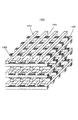
3次元フォトニック結晶において、その代表的な構造の一つとして、特許文献1に開示されているウッドパイル構造(あるいはロッドパイル構造)が知られている。
この3次元フォトニック結晶におけるウッドパイル構造は、図3に示すような3次元周期構造1300を有しており、複数のロッド1301を平行且つ所定の面内周期で周期的に配置したストライプ層を積層して構成されている。1305はロッドの断面である。
各ストライプ層に属する各ロッド1301が最隣接のストライプ層に属する各ロッドと直交し、また、各ストライプ層に属する各ロッド1301が2層離れたストライプ層に属する各ロッド1301と平行且つ面内周期の1/2だけずれるように構成されている。
前記フォトニック結晶の構造の周期は、制御したい電磁波の波長の半分程度である。
As a typical structure of a three-dimensional photonic crystal, a wood pile structure (or a rod pile structure) disclosed in
The woodpile structure in this three-dimensional photonic crystal has a three-dimensional
Each
The period of the structure of the photonic crystal is about half of the wavelength of the electromagnetic wave to be controlled.
また、このような3次元フォトニック結晶の製造方法として、特許文献2では、図4に示すような3次元フォトニック結晶の製造方法を開示している。
この特許文献2においては、3次元フォトニック結晶の製造に際し、薄膜形成及び薄膜加工の後、犠牲層を形成する。
そして、化学機械研磨(CMP:Chemical Mechanical Polishing)で犠牲層を研磨して、加工した薄膜が露出するまで犠牲層を平坦化する。
上記プロセスを繰り返すことによって、犠牲層を用いない製造方法と比べて、高い加工精度で3次元フォトニック結晶を製造可能にしている。
また、特許文献3では、フォトニック結晶の製造方法として、図5に示すような方法を開示している。この特許文献3においては、まず、基板上に設けたストライプ層に平行且つ所定の面内周期で配置したロッドアレイを形成する。
そして、熱接着法で上記ストライプ層同士を層間位置合せしながら接合した後、一方のストライプ層の基板を除去する。
このような工程を繰り返すことによって、接合の回数だけの層数を備えたウッドパイル構造が製造される。
In Patent Document 2, a sacrificial layer is formed after thin film formation and thin film processing in manufacturing a three-dimensional photonic crystal.
Then, the sacrificial layer is polished by chemical mechanical polishing (CMP: Chemical Mechanical Polishing), and the sacrificial layer is planarized until the processed thin film is exposed.
By repeating the above process, a three-dimensional photonic crystal can be manufactured with high processing accuracy compared to a manufacturing method that does not use a sacrificial layer.
Patent Document 3 discloses a method as shown in FIG. 5 as a method for producing a photonic crystal. In Patent Document 3, first, a rod array arranged in parallel with a stripe layer provided on a substrate and arranged at a predetermined in-plane period is formed.
Then, the stripe layers are bonded together by aligning the layers by thermal bonding, and then the substrate of one stripe layer is removed.
By repeating such a process, a woodpile structure having the number of layers equal to the number of times of joining is manufactured.
しかしながら、上記した従来例における3次元フォトニック結晶の製造方法においては、つぎのような課題を有している。
上記従来例の特許文献2のものにおいては、犠牲層の平坦化工程において、下地ロッド構造層が露出するまで平坦化を行うと、ロッド間の犠牲層の表面が凹むことにより、次に積層するロッドの下面が前記凹み形状にならって平坦にならないという問題が生じる。
また、特許文献3のものにおいては、1層形成毎に熱融着による接合と、一方のストライプ層の基板の不要部分の除去を繰り返し行うことから、熱融着によるロッドの変形が発生するという問題が生じる。
However, the above-described conventional method for producing a three-dimensional photonic crystal has the following problems.
In the conventional example of Patent Document 2, in the sacrificial layer flattening step, when the flattening is performed until the underlying rod structure layer is exposed, the surface of the sacrificial layer between the rods is recessed, so that the layers are stacked next. There arises a problem that the lower surface of the rod does not become flat following the concave shape.
Moreover, in the thing of patent document 3, since deformation | transformation of the joining by thermal fusion and removal of the unnecessary part of the board | substrate of one stripe layer are repeatedly performed for every layer formation, the deformation | transformation of the rod by thermal fusion occurs. Problems arise.
本発明は、上記課題に鑑み、犠牲層の平坦化が可能であり、また熱接合によるロッドの変形を低減することが可能となる3次元フォトニック結晶の製造方法を提供することを目的とするものである。 The present invention has been made in view of the above problems, and an object of the present invention is to provide a method for producing a three-dimensional photonic crystal, in which a sacrificial layer can be flattened and deformation of a rod due to thermal bonding can be reduced. Is.
本発明は、つぎのように構成した3次元フォトニック結晶の製造方法を提供するものである。
本発明の3次元フォトニック結晶の製造方法は、周期的な2次元パターン構造を積層した積層構造による3次元フォトニック結晶の製造方法であって、
基板上に、第1の材料からなる薄膜を形成する第1の工程と、
前記薄膜をエッチングして、前記薄膜に周期的な2次元パターン構造を形成する第2の工程と、
前記2次元パターン構造上に、第2の材料からなる薄膜を形成する第3の工程と、
前記2次元パターン構造上に形成された第2の材料からなる薄膜を平坦化する際に、下地の前記2次元パターン構造が露出する前に該平坦化を停止する第4の工程と、
前記第1の工程から前記第4の工程を少なくとも2回以上繰り返し、前記2次元パターン構造を積層して積層構造を形成する第5の工程と、
を含むことを特徴とする。
また、本発明の3次元フォトニック結晶の製造方法は、前記第5の工程において積層構造を形成した後、該積層構造から前記第2の材料からなる薄膜を選択的に除去する第6の工程と、
前記積層構造を形成する前記2次元パターン構造を、一括で接合させる第7の工程と、
を有することを特徴とする。
また、本発明の3次元フォトニック結晶の製造方法は、前記第1の材料からなる薄膜が、誘電体による薄膜で形成されていることを特徴とする。
また、本発明の3次元フォトニック結晶の製造方法は、前記第2の材料からなる薄膜が、犠牲層による薄膜で形成されていることを特徴とする。
また、本発明の3次元フォトニック結晶の製造方法は、前記第4の工程における前記第2の材料からなる薄膜の平坦化に、ドライエッチング法を用いることを特徴とする。
また、本発明の3次元フォトニック結晶の製造方法は、前記第4の工程における前記第2の材料からなる薄膜の平坦化に、化学的機械的研磨法を用いることを特徴とする。
The present invention provides a method for producing a three-dimensional photonic crystal configured as follows.
The method for producing a three-dimensional photonic crystal of the present invention is a method for producing a three-dimensional photonic crystal having a laminated structure in which periodic two-dimensional pattern structures are laminated,
A first step of forming a thin film of a first material on a substrate;
Etching the thin film to form a periodic two-dimensional pattern structure in the thin film;
A third step of forming a thin film of a second material on the two-dimensional pattern structure;
A fourth step of stopping the planarization before the underlying two-dimensional pattern structure is exposed when planarizing the thin film made of the second material formed on the two-dimensional pattern structure;
A fifth step in which the first step to the fourth step are repeated at least twice, and the two-dimensional pattern structure is laminated to form a laminated structure;
It is characterized by including.
Further, in the method for producing a three-dimensional photonic crystal according to the present invention, after forming the laminated structure in the fifth step, the sixth step of selectively removing the thin film made of the second material from the laminated structure. When,
A seventh step of collectively joining the two-dimensional pattern structure forming the stacked structure;
It is characterized by having.
The method for producing a three-dimensional photonic crystal according to the present invention is characterized in that the thin film made of the first material is formed of a thin film made of a dielectric.
The method for producing a three-dimensional photonic crystal according to the present invention is characterized in that the thin film made of the second material is formed by a thin film made of a sacrificial layer.
The method for producing a three-dimensional photonic crystal according to the present invention is characterized in that a dry etching method is used for planarizing the thin film made of the second material in the fourth step.
The method for producing a three-dimensional photonic crystal according to the present invention is characterized in that a chemical mechanical polishing method is used for planarizing the thin film made of the second material in the fourth step.
本発明の3次元フォトニック結晶の製造方法によれば、犠牲層の平坦化が可能であり、また熱接合によるロッドの変形を低減することが可能となる。 According to the method for producing a three-dimensional photonic crystal of the present invention, the sacrificial layer can be flattened, and deformation of the rod due to thermal bonding can be reduced.
つぎに、本発明の実施の形態における3次元フォトニック結晶の製造方法について説明する。
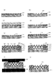
図1に、本実施の形態における3次元フォトニック結晶の製造方法を説明する図を示す。
図1において、110は基板、111、114は誘電体薄膜、112、115、117、119はロッドパターン、113、116、118は犠牲層薄膜、120、121は3次元構造体、122はステージ、123は3次元フォトニック結晶である。
図1(j)に示した3次元フォトニック結晶を形成するために、図1(a)から図1(j)の工程を用いることができる。
本実施の形態では、説明を容易とするため、3次元フォトニック結晶の構造として、ウッドパイル構造の製造工程について説明する。
まず、基板上に、第1の材料からなる薄膜を形成する第1の工程として、図1(a)に示すように、基板110の上にフォトニック結晶を構成する主材料である誘電体薄膜111を形成する(以下において、この工程を誘電体形成工程と記す。)。
必要に応じて、基板110と誘電体薄膜111との界面に、密着性を向上させるための密着層を形成しても良い。
前記基板110としては、例えば、合成石英、サファイア、ガラス、アクリル、Si、GaN、GaAs、InP、InGaAs、TiO2、ZnOの単体、またはこれらの薄膜を有する他の材料を用いることができる。
また、この基板110には、成膜面が平坦性を持つものを用いる。
Next, a method for manufacturing a three-dimensional photonic crystal in the embodiment of the present invention will be described.
FIG. 1 is a diagram illustrating a method for manufacturing a three-dimensional photonic crystal in the present embodiment.
In FIG. 1, 110 is a substrate, 111 and 114 are dielectric thin films, 112, 115, 117 and 119 are rod patterns, 113, 116 and 118 are sacrificial thin films, 120 and 121 are three-dimensional structures, 122 is a stage, 123 is a three-dimensional photonic crystal.
In order to form the three-dimensional photonic crystal shown in FIG. 1 (j), the steps from FIG. 1 (a) to FIG. 1 (j) can be used.
In this embodiment, for ease of explanation, a manufacturing process of a woodpile structure will be described as the structure of a three-dimensional photonic crystal.
First, as a first step of forming a thin film made of a first material on a substrate, as shown in FIG. 1A, a dielectric thin film which is a main material constituting a photonic crystal on a
If necessary, an adhesion layer for improving adhesion may be formed at the interface between the
As the
In addition, a
誘電体薄膜111の材料としては、例えば、酸化チタン、または、窒化ガリウム、または酸化亜鉛、または、酸化インジウムスズ、酸化シリコン、などを用いることができる。
誘電体薄膜111の形成方法として、スパッタ、または真空蒸着、または化学気相堆積、またはエピタキシャル成長、などを用いることができる。
誘電体薄膜111の厚さは、数十nm〜数十μmとすることが望ましい。
次に、前記誘電体薄膜上にエッチング時のマスクを形成する。
エッチング時のマスクをフォトレジストで行う場合は、フォトレジスト膜を形成し、フォトリソグラフィを行うことで、レジストマスクを形成する。
このフォトリソグラフィの露光装置は、EB描画装置、又はスキャニングステッパ−、又はナノインプリント装置、又は露光装置などが適切である。
このレジストマスクの寸法は、例えば、幅は数十nmから数μmであり、面内周期は数百nm〜数μmで、長さは5μm〜1000μm程度である。
また、誘電体薄膜111のエッチングに、マスクとのエッチング選択比が必要な場合には、レジストマスクの代りに、例えば、クロム膜や、タングステンなどの金属マスクを使用するのも良い。
As a material of the dielectric
As a method of forming the dielectric
The thickness of the dielectric
Next, a mask for etching is formed on the dielectric thin film.
In the case where a mask for etching is formed using a photoresist, a photoresist film is formed and photolithography is performed to form a resist mask.
As the photolithography exposure apparatus, an EB drawing apparatus, a scanning stepper, a nanoimprint apparatus, or an exposure apparatus is suitable.
The dimensions of the resist mask are, for example, a width of several tens of nm to several μm, an in-plane period of several hundred nm to several μm, and a length of about 5 μm to 1000 μm.
When the etching selectivity of the dielectric
次に、上記第1の材料からなる薄膜をエッチングして、該薄膜に周期的な2次元パターン構造を形成する第2の工程として、図1(b)に示すように、誘電体薄膜111をエッチングして、マスクを除去することで、ロッドパターン112を形成する。
エッチングは、例えば、フッ化炭素系ガスを主体とした反応性イオンエッチング(RIE)を用いる。
このエッチングによって、基板110上に、フォトニック結晶第1層目のパターンとして、ロッドパターン112を形成する(以下では、この工程をパターン形成工程と記す。)。
Next, as a second step of etching the thin film made of the first material to form a periodic two-dimensional pattern structure on the thin film, a dielectric
For the etching, for example, reactive ion etching (RIE) mainly using a fluorocarbon gas is used.
By this etching, a
次に、前記2次元パターン構造上に、第2の材料からなる薄膜を形成する第3の工程として、図1(c)に示すように、犠牲層薄膜113を形成する(以下では、この工程を犠牲層形成工程と記す。)。
すなわち、前記第1層目のロッドパターン112が形成された構造を含む誘電体薄膜上に、犠牲層薄膜113を形成する。
前記犠牲層薄膜113は、次の図1(d)に示す工程において前記誘電体薄膜111に対して平坦化しやすい材料によって形成されている。
例えば、この犠牲層薄膜113として、銅の薄膜が好適である。この銅薄膜の厚みは、例えば、誘電体薄膜パターンの厚みの1.5〜5倍が好ましい。
この銅薄膜の成膜としては、スパッタ、または真空蒸着、または化学気相堆積、またはエピタキシャル成長などの方法を用いることができる。
また、この犠牲層薄膜113としては、他には、ポリマーを用いても良い。このときの、ポリマーの厚みは、誘電体薄膜のパターンにもよるが、例えば、誘電体薄膜パターンの厚みの1.5〜5倍が好ましい。ポリマーの成膜は、スピンコートやフィルムレジストの貼り付け等がある。
Next, as a third step of forming a thin film made of the second material on the two-dimensional pattern structure, a sacrificial layer
That is, the sacrificial layer
The sacrificial layer
For example, a copper thin film is suitable as the sacrificial layer
For the formation of the copper thin film, a method such as sputtering, vacuum evaporation, chemical vapor deposition, or epitaxial growth can be used.
In addition, as the sacrificial layer
次に、前記2次元パターン構造上に形成された第2の材料からなる薄膜を平坦化する際に、下地の前記2次元パターン構造が露出する前に該平坦化を停止する第4の工程として、前記犠牲層薄膜を平坦化する(以下では、この工程を平坦化工程と記す。)。
図1(d)に示すように、犠牲層薄膜113を平坦化する。
この平坦化工程では、上記犠牲層薄膜113が平坦化され、かつ、下地の誘電体薄膜によるロッドパターン112が露出する前に、平坦化工程を停止する。
上記平坦化加工法は、犠牲層薄膜材料によるが、犠牲層薄膜に銅を用いる場合には、例えば、化学機械研磨(CMP:Chemical Mechanical Polishing。以下これをCMPと記す)を用いることができる。
また、犠牲層薄膜にポリマーを用いる場合には、例えば、ドライエッチング法を用いることができる。
次に、図1(e)に示す工程において、上記した犠牲層薄膜113の素子部の外側部分をエッチングによって除去する。
これは、前に形成した誘電体薄膜111と、次の図1(f)で形成する誘電体薄膜114を接続するために行う工程である。
Next, when flattening the thin film made of the second material formed on the two-dimensional pattern structure, as a fourth step of stopping the flattening before the underlying two-dimensional pattern structure is exposed. The sacrificial layer thin film is flattened (hereinafter, this step is referred to as a flattening step).
As shown in FIG. 1D, the sacrificial layer
In this flattening step, the flattening step is stopped before the sacrificial layer
The planarization method depends on the sacrificial layer thin film material. However, when copper is used for the sacrificial layer thin film, for example, chemical mechanical polishing (CMP: Chemical Mechanical Polishing; hereinafter referred to as CMP) can be used.
Further, when a polymer is used for the sacrificial layer thin film, for example, a dry etching method can be used.
Next, in the step shown in FIG. 1E, the outer portion of the element portion of the sacrificial layer
This is a process performed to connect the dielectric
次に、図1(f)に示す工程において、1層目のロッドパターン112を含む誘電体薄膜111上に、前記誘電体形成工程と同様の工程により、誘電体薄膜114を成膜する。そして、前記パターン形成工程と同様の工程によりフォトニック結晶の第2層目のパターンとして、ロッドパターン115を形成する。
その後、この第2層目の上層にフォトニック結晶の第3層目のロッドパターン117を形成するため、前記犠牲層形成工程及び前記平坦化工程と同様の工程を繰り返す。
Next, in the step shown in FIG. 1F, the dielectric
Thereafter, in order to form the third
そして、第5の工程として、前記第1の工程から前記第4の工程を少なくとも2回以上繰り返し、前記2次元パターン構造を積層して積層構造を形成する。
すなわち、上記した誘電体形成工程、パターン形成工程、犠牲層形成工程、及び平坦化工程を繰り返すことで、積層構造を形成する。
例えば、上記工程を3回繰り返すことで、図1(g)に示すような、ロッドパターン112、115、117、119が合計4層積層され、さらにそのロッドパターンの上下間に前記犠牲層113、116、118が挟まれた3次元構造体120が形成される。
これにより、厚み方向で1周期のウッドパイル構造フォトニック結晶構造が得られる。
但し、最上層の誘電体薄膜パターンを形成する場合、前記犠牲層形成工程と平坦化工程を省いても支障がない。
ここで、層間のパターン位置合せを高い精度で行うために、予め基板や誘電体薄膜上に形成した位置合せマーク(図示なし)を基準にして各層のパターン配置を決めればよい。
As a fifth step, the first step to the fourth step are repeated at least twice, and the two-dimensional pattern structure is stacked to form a stacked structure.
That is, by repeating the above-described dielectric formation process, pattern formation process, sacrificial layer formation process, and planarization process, a laminated structure is formed.
For example, by repeating the above process three times, a total of four layers of
Thereby, a woodpile structure photonic crystal structure having one period in the thickness direction is obtained.
However, when the uppermost dielectric thin film pattern is formed, there is no problem even if the sacrifice layer forming step and the planarization step are omitted.
Here, in order to perform pattern alignment between layers with high accuracy, the pattern arrangement of each layer may be determined with reference to an alignment mark (not shown) formed in advance on a substrate or a dielectric thin film.
ここで、注目すべきことは、2層目以降のパターン形成工程における下地犠牲層パターンの影響についてである。
上記平坦化工程において、下地のパターンが露出するまで平坦化を行うと、例えば、CMPで行った場合、ディッシングとよばれる凹み形状が、犠牲層上部に形成される。
その上層のパターン形成工程において、その凹み形状に倣って形成されるために、ロッドパターンにこの凹み形状が転写されてしまう。
これはフォトニック結晶構造の加工精度を低下させ、素子特性に影響を及ぼすことになる。
これに対して、本実施の形態の上記平坦化工程において、犠牲層薄膜の平坦化が完了し、かつ、下地の誘電体パターンが表出する前に、平坦化工程を停止することで、この犠牲層に凹み形状の発生を防止することが可能となる。
これにより、ロッドパターンに、凹み形状の転写が抑制されるので、フォトニック結晶構造の加工精度の低下を避けることが可能になる。
What should be noted here is about the influence of the base sacrificial layer pattern in the pattern forming process for the second and subsequent layers.
In the planarization step, when planarization is performed until the underlying pattern is exposed, for example, when performing CMP, a concave shape called dishing is formed on the sacrificial layer.
In the upper layer pattern forming step, the concave shape is transferred to the rod pattern because it is formed following the concave shape.
This lowers the processing accuracy of the photonic crystal structure and affects the device characteristics.
On the other hand, in the planarization process of the present embodiment, the planarization process is stopped before the planarization of the sacrificial layer thin film is completed and the underlying dielectric pattern is exposed. It is possible to prevent the formation of a concave shape in the sacrificial layer.
Thereby, since the transfer of the concave shape to the rod pattern is suppressed, it is possible to avoid a reduction in processing accuracy of the photonic crystal structure.
次に、前記第5の工程において積層構造を形成した後、該積層構造から前記第2の材料からなる薄膜を選択的に除去する第6の工程として、ロッドパターン間の犠牲層を除去する(以下では、これを犠牲層除去工程と記す。)。
すなわち、図1(h)に示すように、ロッドパターン間の犠牲層を一括で除去する。
この犠牲層の除去方法としては、犠牲層薄膜材料にもよるが、例えば、ウェットエッチング法や、等方性のドライエッチング、などを用いることができる。
この犠牲層除去工程により、ロッドパターン間に、犠牲層厚さ分の空隙ができる。
犠牲層除去工程で、ウェットエッチング法を用いる場合には、エッチング後の乾燥工程で、ロッドパターン間でのスティッキング防止のために、超臨界乾燥を行ってもよい。
Next, after forming a laminated structure in the fifth step, a sacrificial layer between rod patterns is removed as a sixth step of selectively removing the thin film made of the second material from the laminated structure ( Hereinafter, this is referred to as a sacrificial layer removing step.)
That is, as shown in FIG. 1H, the sacrificial layer between the rod patterns is removed at once.
As a method for removing the sacrificial layer, although depending on the sacrificial layer thin film material, for example, a wet etching method or an isotropic dry etching can be used.
By this sacrificial layer removal step, a gap corresponding to the thickness of the sacrificial layer is formed between the rod patterns.
When a wet etching method is used in the sacrificial layer removing step, supercritical drying may be performed in the drying step after etching to prevent sticking between the rod patterns.
次に、前記積層構造を形成する前記2次元パターン構造を、一括で接合させる第7の工程として、各ロッドパターンを一括で接合させる。
すなわち、図1(i)に示すように、基板を接合装置の真空チャンバーにセットし、チャンバー内を例えば、10−5Pa台に真空引きする。
次に、基板110に、ステージ122の上側を下降させ、各ロッドパターンを一括で接合させる。このとき、誘電体材料に応じて、応力や温度を設定する。
また、材料に応じて、接合前にロッドパターン表面に清浄化処理を施すのも良い。
各ロッドパターン層ごとに接合させる場合と比較して、本実施の形態の方法によれば、ロッドパターン層を一括で接合するために、熱工程を伴う接合の場合には、熱工程が1回で済むことから、熱によるロッドパターンの変形を最小限にすることができる。
以上の積層工程によって、誘電体薄膜からなる3次元フォトニック結晶構造が作製される。
以上では、説明を容易とするために、3次元ウッドパイル構造だけを示したが、本発明はこれに限られるものではない。本発明においては、それ以外の3次元構造でも容易に形成することが可能である。
Next, as a seventh step of collectively bonding the two-dimensional pattern structures forming the stacked structure, the rod patterns are bonded together.
That is, as shown in FIG. 1I, the substrate is set in a vacuum chamber of a bonding apparatus, and the inside of the chamber is evacuated to, for example, 10 −5 Pa.
Next, the upper side of the
Depending on the material, the surface of the rod pattern may be cleaned before joining.
Compared with the case where each rod pattern layer is joined, according to the method of the present embodiment, in order to join the rod pattern layers together, in the case of joining involving a thermal process, the thermal process is performed once. Therefore, deformation of the rod pattern due to heat can be minimized.
A three-dimensional photonic crystal structure made of a dielectric thin film is produced by the above-described lamination process.
In the above, for ease of explanation, only the three-dimensional woodpile structure is shown, but the present invention is not limited to this. In the present invention, other three-dimensional structures can be easily formed.
以下に、本発明の実施例について説明するが、本発明はこれらによって何ら限定されるものではない。
[実施例1]
実施例1においては、ウッドパイル型の3次元フォトニック結晶の製造方法について説明する。
本実施例においては、上記本発明の実施の形態で説明した3次元フォトニック結晶の製造方法と、基本的に同じ工程によるものであるから、ここでも図1を用いて説明する。
まず、図1(a)に示す誘電体形成工程において、例えば、合成石英からなる基板110上に、第1の材料からなる誘電体薄膜111として、例えば、酸化チタン薄膜を、例えばスパッタ法により、80nm厚さに成膜する。
次に、誘電体薄膜111上に、フォトレジスト膜を塗布形成し、フォトリソグラフィを行うことで、所望のレジストパターンを形成する(不図示)。このときに、次の重ね合わせの露光に用いる位置合わせマーク(不図示)のパターンも形成しておく。
次に、このレジストパターンをエッチングマスクとして、誘電体薄膜111の酸化チタン薄膜を、例えば、フッ化炭素ガスを主体とする反応性イオンエッチングを用いてパターニングする。
次に、図1(b)に示すパターン形成工程なおいて、つぎのように1層目のロッドパターン112を形成する。
すなわち、上記レジストパターン(不図示)を、例えば有機溶剤を用いて除去し、前記基板110上に誘電体薄膜111の酸化チタンからなる、幅80nm、ピッチ250nm、高さ80nmの1層目のロッドパターン112を形成する。
次に、図1(c)に示す犠牲層形成工程において、前記基板110上に、スピンコート法で例えばフォトレジスト膜を形成し、ベーク処理を行うことで、第2の材料からなる薄膜として、フォトレジスト膜からなる犠牲層113を形成する。ここで、前記犠牲層113の平坦性を良くするために、少なくとも2回以上、塗布及び、ベークを繰り返すことで、パターン上のレジストを平坦化させる。このとき塗布するフォトレジスト膜厚は、数μm以上が望ましい。
なお、この犠牲層に用いるフォトレジスト膜は、次にロッド構造を形成する際のエッチングマスクとなるフォトレジストを除去する際に、除去されない材料を選択する。なおかつ、この犠牲層を除去する際に、ロッド構造が除去されない材料を選択する。
Examples of the present invention will be described below, but the present invention is not limited to these examples.
[Example 1]
In Example 1, a method for manufacturing a woodpile type three-dimensional photonic crystal will be described.
Since this embodiment is based on basically the same process as the manufacturing method of the three-dimensional photonic crystal described in the embodiment of the present invention, it will be described here with reference to FIG.
First, in the dielectric formation step shown in FIG. 1A, for example, a titanium oxide thin film is formed as a dielectric
Next, a photoresist film is applied and formed on the dielectric
Next, using this resist pattern as an etching mask, the titanium oxide thin film of the dielectric
Next, in the pattern forming step shown in FIG. 1B, the first
That is, the resist pattern (not shown) is removed using, for example, an organic solvent, and a first layer rod having a width of 80 nm, a pitch of 250 nm, and a height of 80 nm made of titanium oxide of the dielectric
Next, in the sacrificial layer forming step shown in FIG. 1C, a thin film made of the second material is formed by, for example, forming a photoresist film on the
For the photoresist film used for the sacrificial layer, a material that is not removed when the photoresist that becomes an etching mask for the next formation of the rod structure is removed is selected. In addition, when removing the sacrificial layer, a material from which the rod structure is not removed is selected.
次に、図1(d)に示す平坦化工程において、前記犠牲層113を、酸素ガスを主体とした反応性イオンエッチングで、誘電体薄膜111の酸化チタン薄膜の表面から、例えば10nm高さになるまでエッチバックする。
この犠牲層の残膜厚の制御には、エッチング時間制御に加え、エリプソメーターによる膜厚測定を組み合わせても良い。
次に、図1(e)に示すように、前記犠牲層113に、レジストパターン(不図示)をフォトリソグラフィで形成する。
そして、素子部の外側の前記犠牲層113を、例えば酸素ガスを主体とした反応性イオンエッチングで除去し、素子部の外側の誘電体薄膜111を露出させる。 次に、図1(f)に示す工程において、1層目のロッドパターン112を含む誘電体薄膜111上に、前記誘電体形成工程と同様の工程により、誘電体薄膜114を成膜する。そして、前記パターン形成工程と同様の工程によりフォトニック結晶の第2層目のパターンとして、ロッドパターン115を形成する。
具体的には、まず、1層目のロッドパターン112を含む誘電体薄膜111上に、誘電体薄膜114として、例えば、酸化チタンをスパッタ法で、例えば80nmの膜厚になるように成膜する。
次に、この誘電体薄膜114上に、フォトレジスト膜を塗布形成し、前記した誘電体薄膜111に形成された位置合わせマーク(不図示)を用いて位置合わせを行いながら、フォトリソグラフィを行うことで、所望のレジストパターンを形成する(不図示)。
次に、このレジストパターンをエッチングマスクとして、上記した誘電体薄膜114の酸化チタン薄膜を、例えば、フッ化炭素ガス系を主体とする反応性イオンエッチングを用いてパターニングする。
次に、このレジストパターン(不図示)を、例えば有機溶剤を用いて除去し、前記基板110上に、幅80nm、ピッチ250nm、高さ80nmの2層目のロッドパターン115が形成される。
このとき、図1(e)の工程で、素子部の外側の前記犠牲層113を除去しているので、第1の材料からなる誘電体薄膜111、113は、素子部の外側部分で繋がっている。
その後、この第2層目の上層にフォトニック結晶の第3層目のロッドパターン115を形成するため、前記犠牲層形成工程及び前記平坦化工程と同様の工程を繰り返す。
このように、誘電体形成工程、パターン形成工程、犠牲層形成工程、及び平坦化工程を3回繰り返すことで、図1(g)に示す3次元構造体120が形成される。
すなわち、ロッドパターン112、115、117、119が合計4層積層され、さらにそのロッドパターンの上下間に前記犠牲層113、116、118が挟まれた3次元構造体120が形成される。
Next, in the planarization step shown in FIG. 1D, the
Control of the remaining film thickness of the sacrificial layer may be combined with film thickness measurement using an ellipsometer in addition to etching time control.
Next, as shown in FIG. 1E, a resist pattern (not shown) is formed on the
Then, the
Specifically, first, for example, titanium oxide is deposited on the dielectric
Next, a photoresist film is applied and formed on the dielectric
Next, using the resist pattern as an etching mask, the titanium oxide thin film of the dielectric
Next, the resist pattern (not shown) is removed using, for example, an organic solvent, and a second-
At this time, since the
Thereafter, in order to form the third
Thus, the three-
That is, a total of four layers of
次に、前記3次元構造体120が形成された基板110を真空チャンバー内にセットし、例えば酸素ガスを用いた等方性のアッシング法で、犠牲層113、116、118を除去する。
これにより、図1(h)に示すようにロッドパターン112、115、117、119間に、犠牲層厚さとほぼ同等の空隙がある3次元構造体121が形成される。
Next, the
Thereby, as shown in FIG. 1 (h), a three-
次に、図1(i)に示すように、基板を接合装置の真空チャンバーのステージ122にセットし、チャンバー内を例えば、10−5Pa台に真空引きする。
次に、前記3次元構造体121の上部に、ステージ122の上側を下降させて接触させ、前記3次元構造体121に荷重を印加し、この工程により、前記3次元構造体120の各ロッドパターン112、115、117、119を一括で接合させる。
このときの荷重範囲は、例えば、10〜500kg/cm2fであり、この接合時の温度範囲は、例えば200〜800℃である。
Next, as shown in FIG. 1I, the substrate is set on the
Next, the upper side of the
The load range at this time is, for example, 10 to 500 kg / cm 2 f, and the temperature range at the time of joining is, for example, 200 to 800 ° C.
以上の工程により、図1(j)に示すように、4層のロッドパターン112、115、117、119が積層されたウッドパイル構造の酸化チタンからなる3次元フォトニック結晶123が形成される。
Through the above steps, as shown in FIG. 1J, a three-
以上の本実施例によるフォトニック結晶の製造方法によれば、犠牲層埋め込み時の平坦化で発生する凹みによるロッドパターンの形状劣化を、下地の構造体層が露出前に平坦化を停止することで低減できる。
また、フォトニック結晶を構成する各ロッド層の接合を一括で行うことで、熱の印加を伴う接合工程が1回で済むことから、フォトニック結晶を構成するロッドの変形が最小限で済むので、高精度にフォトニック結晶を製造することが可能となる。
According to the photonic crystal manufacturing method of the present embodiment described above, the deterioration of the shape of the rod pattern due to the dent generated during the planarization when the sacrificial layer is embedded is stopped before the underlying structure layer is exposed. Can be reduced.
In addition, since the rod layers constituting the photonic crystal are joined together, the joining process involving application of heat can be performed only once, so that the deformation of the rod constituting the photonic crystal can be minimized. It becomes possible to manufacture a photonic crystal with high accuracy.
[実施例2]
実施例2においては、実施例1とは異なる形態のウッドパイル型の3次元フォトニック結晶の製造方法について説明する。
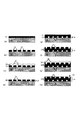
図2に、本実施例の3次元フォトニック結晶の製造方法を説明する図を示す。
図2において、210は基板、211、214は誘電体薄膜、212、215、217、219はロッドパターン、213、216、218は犠牲層薄膜、220、221は3次元構造体、222はステージ、223は3次元フォトニック結晶である。
[Example 2]
In Example 2, a method for manufacturing a woodpile type three-dimensional photonic crystal having a different form from Example 1 will be described.
FIG. 2 is a diagram illustrating a method for manufacturing the three-dimensional photonic crystal of this example.
In FIG. 2, 210 is a substrate, 211 and 214 are dielectric thin films, 212, 215, 217 and 219 are rod patterns, 213, 216 and 218 are sacrificial layer thin films, 220 and 221 are three-dimensional structures, 222 is a stage,
まず、図2(a)に示す誘電体形成工程において、例えば、合成石英からなる基板210上に、第1の材料からなる誘電体薄膜211として、例えば、酸化チタン薄膜を、例えばスパッタ法により、80nm厚さに成膜する。
次に、誘電体薄膜211上に、フォトレジスト膜を塗布形成し、フォトリソグラフィを行うことで、所望のレジストパターンを形成する(不図示)。このときに、次の重ね合わせの露光に用いる位置合わせマーク(不図示)のパターンも形成しておく。
次に、このレジストパターンをエッチングマスクとして、誘電体薄膜211の酸化チタン薄膜を、例えば、フッ化炭素系ガスを主体とする反応性イオンエッチングを用いてパターニングする。
次に、図2(b)に示すパターン形成工程において、つぎのように1層目のロッドパターン212を形成する。
すなわち、上記レジストパターン(不図示)を、例えば有機溶剤を用いて除去して、前記基板210上に誘電体薄膜211の酸化チタンからなる、幅80nm、ピッチ250nm、高さ80nmの1層目のロッドパターン212を形成する。次に、図2(c)に示すパターン形成工程において、前記基板210上に、第2の材料からなる薄膜とし、犠牲層213としての、例えばスパッタリング法で、例えば銅薄膜を形成する。
この銅薄膜の厚さは、例えば、300nmであり、第1の材料からなる薄膜211との密着性向上のため、銅薄膜成膜前にチタン薄膜を例えば5nm厚さに成膜する。
なお、この犠牲層213に用いる材料は、最終的にこの犠牲層を除去するときに、第1の材料がエッチングされにくい材料を選択する必要がある。
次に、図2(d)に示す平坦化工程において、前記犠牲層213を、化学的機械的研磨法により研磨し、この犠牲層213の厚さが、第1の材料からなる薄膜211の酸化チタン薄膜の表面から、例えば10nm高さになるまで研磨する。
この残膜厚の制御は、例えば、研磨時間で制御する。
次に、図2(e)に示すように、前記犠牲層213に、レジストパターン(不図示)をフォトリソグラフィで形成し、素子部の外側の前記犠牲層213を、例えば、塩化鉄を含むエッチング溶液で除去し、素子部の外側の第1の材料からなる薄膜211を露出させる。
First, in the dielectric formation step shown in FIG. 2A, for example, a titanium oxide thin film is formed as a dielectric
Next, a photoresist film is applied and formed on the dielectric
Next, using this resist pattern as an etching mask, the titanium oxide thin film of the dielectric
Next, in the pattern forming step shown in FIG. 2B, a first
That is, the resist pattern (not shown) is removed by using, for example, an organic solvent, and a first layer having a width of 80 nm, a pitch of 250 nm, and a height of 80 nm made of titanium oxide of the dielectric
The thickness of the copper thin film is, for example, 300 nm, and a titanium thin film is formed to a thickness of, for example, 5 nm before forming the copper thin film in order to improve the adhesion with the
Note that, as a material used for the
Next, in the planarization step shown in FIG. 2D, the
The remaining film thickness is controlled by, for example, the polishing time.
Next, as shown in FIG. 2E, a resist pattern (not shown) is formed on the
次に、図2(f)に示す工程において、1層目のロッドパターン212を含む誘電体薄膜211上に、前記誘電体形成工程と同様の工程により、誘電体薄膜214を成膜する。そして、前記パターン形成工程と同様の工程によりフォトニック結晶の第2層目のパターンとして、ロッドパターン215を形成する。
具体的には、まず、1層目のロッドパターン212を含む誘電体薄膜211上に、誘電体薄膜214として、例えば、酸化チタンをスパッタ法で、例えば80nmの膜厚になるように成膜する。
次に、誘電体薄膜214上に、フォトレジスト膜を塗布形成し、上記した誘電体薄膜211に形成された位置合わせマーク(不図示)を用いて位置合わせを行いながら、フォトリソグラフィを行うことで、所望のレジストパターンを形成する(不図示)。
次に、このレジストパターンをエッチングマスクとして、誘電体薄膜214の酸化チタン薄膜を、例えば、フッ化炭素ガス系を主体とする反応性イオンエッチングを用いてパターニングする。
次に、このレジストパターン(不図示)を、例えば有機溶剤を用いて除去して、前記1層目のロッドパターン212を含む誘電体薄膜211上に、幅80nm、ピッチ250nm、高さ80nmの2層目のロッドパターン215を形成する。このとき、図2(e)の工程で、素子部の外側の前記犠牲層213を除去しているので、第1の材料からなる薄膜211、214は、素子部の外側部分で繋がっている。
その後、この第2層目の上層にフォトニック結晶の第3層目のロッドパターン215を形成するため、前記犠牲層形成工程及び前記平坦化工程と同様の工程を繰り返す。
このように、誘電体形成工程、パターン形成工程、犠牲層形成工程、及び平坦化工程を3回繰り返すことで、図2(g)に示す構造220が形成される。
すなわち、ロッドパターン212、215、217、219が合計4層積層され、さらにそのロッドパターンの上下間に前記犠牲層213、216、218が挟まれた構造220が形成される。
Next, in the step shown in FIG. 2F, the dielectric
Specifically, first, for example, titanium oxide is deposited on the dielectric
Next, a photoresist film is applied and formed on the dielectric
Next, using this resist pattern as an etching mask, the titanium oxide thin film of the dielectric
Next, the resist pattern (not shown) is removed by using, for example, an organic solvent, and the dielectric
Thereafter, in order to form the third
Thus, the
That is, a total of four layers of
次に、前記3次元構造体220が形成された基板210の犠牲層213、216、218を例えば、塩化鉄を含むエッチング溶液で除去する。エッチング後の乾燥は、例えば超臨界乾燥で行う。
これにより、図2(h)に示すようにロッドパターン212、215、217、219間に、犠牲層厚さとほぼ同等の空隙がある構造221が形成される。
Next, the
Thereby, as shown in FIG. 2 (h), a
次に、図2(i)に示すように、基板を接合装置の真空チャンバーのステージ222にセットし、チャンバー内を真空引きする。このときの圧力範囲は、例えば、10−2台〜10−6Pa台である。
次に、前記3次元構造体221の上部に、ステージ222の上側を下降させて接触させ、前記3次元構造体221に荷重を印加し、この工程により、前記3次元構造体220の各ロッドパターン212、215、217、219を一括で接合させる。
このときの荷重範囲例えば、10〜500kg/cm2fであり、この接合時の温度範囲は、例えば200〜800℃である。
以上の工程により、図2(j)に示すように、4層のロッドパターン212、215、217、219が積層されたウッドパイル構造の酸化チタンからなる3次元フォトニック結晶223を形成できる。
Next, as shown in FIG. 2I, the substrate is set on the
Next, the upper side of the
The load range at this time is, for example, 10 to 500 kg / cm 2 f, and the temperature range at the time of joining is 200 to 800 ° C., for example.
Through the above steps, as shown in FIG. 2J, a three-
以上の本実施例によるフォトニック結晶の製造方法によれば、犠牲層埋め込み時の平坦化で発生する凹みによるロッドパターンの形状劣化を、下地の構造体層が露出前に平坦化を停止することで低減できる。
また、フォトニック結晶を構成する各ロッド層の接合を一括で行うことで、熱の印加を伴う接合工程が1回で済むことから、フォトニック結晶を構成するロッドの変形が最小限で済むので、高精度にフォトニック結晶を製造することが可能となる。
According to the photonic crystal manufacturing method of the present embodiment described above, the deterioration of the shape of the rod pattern due to the dent generated during the planarization when the sacrificial layer is embedded is stopped before the underlying structure layer is exposed. Can be reduced.
In addition, since the rod layers constituting the photonic crystal are joined together, the joining process involving application of heat can be performed only once, so that the deformation of the rod constituting the photonic crystal can be minimized. It becomes possible to manufacture a photonic crystal with high accuracy.
110、210:基板
111、114、211、214:誘電体薄膜
112、115、117、119:ロッドパターン
211、215、217、219:ロッドパターン
113、116、118、213、216、218:犠牲層薄膜
120、220:3次元構造体
121、221:3次元構造体
122、222:ステージ
123、223:3次元フォトニック結晶
110, 210:
Claims (6)
基板上に、第1の材料からなる薄膜を形成する第1の工程と、
前記薄膜をエッチングして、前記薄膜に周期的な2次元パターン構造を形成する第2の工程と、
前記2次元パターン構造上に、第2の材料からなる薄膜を形成する第3の工程と、
前記2次元パターン構造上に形成された第2の材料からなる薄膜を平坦化する際に、下地の前記2次元パターン構造が露出する前に該平坦化を停止する第4の工程と、
前記第1の工程から前記第4の工程を少なくとも2回以上繰り返し、前記2次元パターン構造を積層して積層構造を形成する第5の工程と、
を含むことを特徴とする3次元フォトニック結晶の製造方法。 A method for producing a three-dimensional photonic crystal having a laminated structure in which periodic two-dimensional pattern structures are laminated,
A first step of forming a thin film of a first material on a substrate;
Etching the thin film to form a periodic two-dimensional pattern structure in the thin film;
A third step of forming a thin film of a second material on the two-dimensional pattern structure;
A fourth step of stopping the planarization before the underlying two-dimensional pattern structure is exposed when planarizing the thin film made of the second material formed on the two-dimensional pattern structure;
A fifth step in which the first step to the fourth step are repeated at least twice, and the two-dimensional pattern structure is laminated to form a laminated structure;
A method for producing a three-dimensional photonic crystal, comprising:
前記積層構造を形成する前記2次元パターン構造を、一括で接合させる第7の工程と、
を有することを特徴とする請求項1に記載の3次元フォトニック結晶の製造方法。 A sixth step of selectively removing the thin film made of the second material from the laminated structure after forming the laminated structure in the fifth step;
A seventh step of collectively joining the two-dimensional pattern structure forming the stacked structure;
The method for producing a three-dimensional photonic crystal according to claim 1, wherein:
Priority Applications (1)
| Application Number | Priority Date | Filing Date | Title |
|---|---|---|---|
| JP2007128989A JP2008286830A (en) | 2007-05-15 | 2007-05-15 | Method of manufacturing three-dimensional photonic crystal |
Applications Claiming Priority (1)
| Application Number | Priority Date | Filing Date | Title |
|---|---|---|---|
| JP2007128989A JP2008286830A (en) | 2007-05-15 | 2007-05-15 | Method of manufacturing three-dimensional photonic crystal |
Publications (1)
| Publication Number | Publication Date |
|---|---|
| JP2008286830A true JP2008286830A (en) | 2008-11-27 |
Family
ID=40146653
Family Applications (1)
| Application Number | Title | Priority Date | Filing Date |
|---|---|---|---|
| JP2007128989A Pending JP2008286830A (en) | 2007-05-15 | 2007-05-15 | Method of manufacturing three-dimensional photonic crystal |
Country Status (1)
| Country | Link |
|---|---|
| JP (1) | JP2008286830A (en) |
-
2007
- 2007-05-15 JP JP2007128989A patent/JP2008286830A/en active Pending
Similar Documents
| Publication | Publication Date | Title |
|---|---|---|
| JP5100146B2 (en) | Optical element and optical element manufacturing method | |
| TW200908093A (en) | Method for fabricating semiconductor device | |
| CN112020770A (en) | Multilayer stacked optical element using temporary and permanent bonding | |
| JP5078058B2 (en) | Mold and mold manufacturing method | |
| US7700390B2 (en) | Method for fabricating three-dimensional photonic crystal | |
| US11417526B2 (en) | Multiple patterning processes | |
| US20180114699A1 (en) | Method for Self-Aligned Cutting of Single Fins | |
| US20090170310A1 (en) | Method of forming a metal line of a semiconductor device | |
| JP2001074954A (en) | Production of three dimensional photonic crystal structure | |
| US20090227110A1 (en) | Method of Forming Mask Pattern | |
| US8698284B2 (en) | Nitride-based semiconductor substrates having hollow member pattern and methods of fabricating the same | |
| TW200847235A (en) | Method for forming fine patterns in semiconductor device | |
| JP2008286830A (en) | Method of manufacturing three-dimensional photonic crystal | |
| JP6123242B2 (en) | Pattern formation method | |
| JP5038218B2 (en) | Manufacturing method of three-dimensional photonic crystal | |
| US20080124823A1 (en) | Method of fabricating patterned layer using lift-off process | |
| KR20190136249A (en) | Ultrafine pattern and fabricating method of the same | |
| US8941920B2 (en) | Method of producing optical element and optical element | |
| JP2005005547A (en) | Manufacturing method of thin film member | |
| JP2007273665A (en) | Mold and method of manufacturing same | |
| US20200343100A1 (en) | Semiconductor device and fabrication method thereof | |
| US9348230B2 (en) | Method of manufacturing semiconductor device | |
| JP4494497B2 (en) | Manufacturing method of three-dimensional structure | |
| JP5983322B2 (en) | Method for forming pattern structure | |
| KR20100076763A (en) | Method for fabricating fine pattern in semiconductor device |