JP2008277748A - Method for forming resist pattern, and semiconductor device manufactured by the method - Google Patents
Method for forming resist pattern, and semiconductor device manufactured by the method Download PDFInfo
- Publication number
- JP2008277748A JP2008277748A JP2008021604A JP2008021604A JP2008277748A JP 2008277748 A JP2008277748 A JP 2008277748A JP 2008021604 A JP2008021604 A JP 2008021604A JP 2008021604 A JP2008021604 A JP 2008021604A JP 2008277748 A JP2008277748 A JP 2008277748A
- Authority
- JP
- Japan
- Prior art keywords
- water repellent
- substrate
- water
- film
- layer
- Prior art date
- Legal status (The legal status is an assumption and is not a legal conclusion. Google has not performed a legal analysis and makes no representation as to the accuracy of the status listed.)
- Pending
Links
Images


Classifications
-
- G—PHYSICS
- G03—PHOTOGRAPHY; CINEMATOGRAPHY; ANALOGOUS TECHNIQUES USING WAVES OTHER THAN OPTICAL WAVES; ELECTROGRAPHY; HOLOGRAPHY
- G03F—PHOTOMECHANICAL PRODUCTION OF TEXTURED OR PATTERNED SURFACES, e.g. FOR PRINTING, FOR PROCESSING OF SEMICONDUCTOR DEVICES; MATERIALS THEREFOR; ORIGINALS THEREFOR; APPARATUS SPECIALLY ADAPTED THEREFOR
- G03F7/00—Photomechanical, e.g. photolithographic, production of textured or patterned surfaces, e.g. printing surfaces; Materials therefor, e.g. comprising photoresists; Apparatus specially adapted therefor
- G03F7/20—Exposure; Apparatus therefor
- G03F7/2041—Exposure; Apparatus therefor in the presence of a fluid, e.g. immersion; using fluid cooling means
-
- G—PHYSICS
- G03—PHOTOGRAPHY; CINEMATOGRAPHY; ANALOGOUS TECHNIQUES USING WAVES OTHER THAN OPTICAL WAVES; ELECTROGRAPHY; HOLOGRAPHY
- G03F—PHOTOMECHANICAL PRODUCTION OF TEXTURED OR PATTERNED SURFACES, e.g. FOR PRINTING, FOR PROCESSING OF SEMICONDUCTOR DEVICES; MATERIALS THEREFOR; ORIGINALS THEREFOR; APPARATUS SPECIALLY ADAPTED THEREFOR
- G03F7/00—Photomechanical, e.g. photolithographic, production of textured or patterned surfaces, e.g. printing surfaces; Materials therefor, e.g. comprising photoresists; Apparatus specially adapted therefor
- G03F7/70—Microphotolithographic exposure; Apparatus therefor
- G03F7/70216—Mask projection systems
- G03F7/70341—Details of immersion lithography aspects, e.g. exposure media or control of immersion liquid supply
-
- H—ELECTRICITY
- H01—ELECTRIC ELEMENTS
- H01L—SEMICONDUCTOR DEVICES NOT COVERED BY CLASS H10
- H01L21/00—Processes or apparatus adapted for the manufacture or treatment of semiconductor or solid state devices or of parts thereof
- H01L21/02—Manufacture or treatment of semiconductor devices or of parts thereof
- H01L21/027—Making masks on semiconductor bodies for further photolithographic processing not provided for in group H01L21/18 or H01L21/34
- H01L21/0271—Making masks on semiconductor bodies for further photolithographic processing not provided for in group H01L21/18 or H01L21/34 comprising organic layers
- H01L21/0273—Making masks on semiconductor bodies for further photolithographic processing not provided for in group H01L21/18 or H01L21/34 comprising organic layers characterised by the treatment of photoresist layers
- H01L21/0274—Photolithographic processes
Abstract
Description
本発明は、液浸露光において要求される、撥水性が高く、かつ膜剥がれ抑制効果の大きいレジストパターンの形成方法と、その方法により製造した半導体デバイスに関する。 The present invention relates to a method for forming a resist pattern, which is required in immersion exposure, has a high water repellency and has a large effect of suppressing film peeling, and a semiconductor device manufactured by the method.
レジストパターンを液浸型露光により形成する場合には、図2に示すような構造の装置が使用される(非特許文献1参照)。この液浸型露光装置は、レンズ21の下方に、ウェハ22が配置され、レンズ21とウェハ22の被照射面の間には、純水23が満たされるように、純水がノズル24の流入口24aから入り、吸入口24bより排出される。被照射面には、微細加工用レジスト膜が、単層レジスト膜または多層レジスト膜として形成される。後者の多層レジスト膜の場合は、微細加工用レジスト膜の構成は複雑化し、下層有機膜層、シリコン含有中間層、感光性レジスト層の最低3種の層からなる。また、液浸型露光(液浸リソグラフィー)では、微細加工用レジスト膜の最上層である感光性レジスト層の上に、液浸のための液と感光性レジスト層との直接接触による液浸のための液の有機汚染を避けるため、トップコート層が形成されることがある。
When the resist pattern is formed by immersion exposure, an apparatus having a structure as shown in FIG. 2 is used (see Non-Patent Document 1). In this immersion type exposure apparatus, a wafer 22 is disposed below a
液浸型露光では、レンズとウェハの微小隙間に水の表面張力を利用して水膜(メニスカス)を形成することにより、レンズと被照射面であるウェハの間を高屈折率化する方式が取られている。このメニスカスを形成する型の液浸装置を用いてウェハ周縁部を露光する場合には、メニスカスの一部がウェハの外にはみ出してしまう欠けショットが存在する。図8(a)に液浸型露光装置の平面図を示す。ステージ80に設置したウェハ81上を液浸シャワーヘッド82が矢印の方向にスキャンする。シャワーヘッド82には、レンズ85が装填され、純水が水流入口84から入り、水吸入口83から排出される。図8(b)は、ウェハ81の周縁部を露光しているときの液浸シャワーヘッド82の部分の拡大図であり、○印を付けた2個のチップは動作チップとして使用できるが、メニスカスがウェハの外にはみ出しているため、×印を付けた4個のチップは捨てられる。このようにウェハ周縁部を露光する場合に、メニスカスの一部がウェハの外にはみ出してしまう欠けショットが生じる。
In immersion type exposure, there is a method to increase the refractive index between the lens and the wafer to be irradiated by forming a water film (meniscus) using the surface tension of water in the minute gap between the lens and the wafer. Has been taken. When the peripheral edge of the wafer is exposed using this type of liquid immersion apparatus for forming a meniscus, there are chipped shots in which a part of the meniscus protrudes from the wafer. FIG. 8A shows a plan view of the immersion type exposure apparatus. A liquid
図8(b)に示すような欠けショットの場合、ウェハ81とレンズ85との間を満たしている水の一部が、ウェハ81とステージ80の外周枠の隙間86からこぼれ落ちることがある。液浸液が多量にこぼれ落ちた場合、メニスカスが崩壊し、液浸露光自体が不可能になる。また、こぼれ落ちる量が少量であっても露光装置や基板裏面を汚染し、後で露光されるウェハにおいて基板裏面の異物に起因したデフォーカスを引き起こす2次被害が起こる。また、欠けショットを液浸露光する際に、ウェハエッジの塗布膜の基板への密着力が弱い場合は膜剥がれが起こり、流速を持つ液浸液の中に、エッジから膜剥がれした異物が混入し、ウェハ液浸液を汚染し、ウェハ中央部にパターン欠陥が発生するという問題がある。
In the case of the chip shot as shown in FIG. 8B, a part of the water filling the space between the
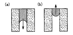
図3に、毛細管内の水の挙動を示す。図3(a)は、毛細管の内面が親水性の場合であり、毛細管力により水は毛細管内を矢印の方向に前進する。一方、図3(b)は、毛細管の内面が撥水性の場合であり、毛細管力により水は後退する。このため、従来は、ウェハとステージの外周枠の間隔を極力狭い構造に装置を設計し、ステージの外周枠に撥水性の部材を使用し、かつウェハ外周部分もウェハ全面に撥水性の塗布膜で被覆することにより、毛細管力を利用して、液浸液のこぼれ落ちを抑制していた。 FIG. 3 shows the behavior of water in the capillary tube. FIG. 3A shows a case where the inner surface of the capillary is hydrophilic, and water advances in the direction of the arrow in the capillary by the capillary force. On the other hand, FIG. 3B shows a case where the inner surface of the capillary is water-repellent, and water is retracted by the capillary force. For this reason, conventionally, the apparatus is designed to have a structure in which the distance between the wafer and the outer peripheral frame of the stage is as narrow as possible, a water-repellent member is used for the outer peripheral frame of the stage, and the water-repellent coating film is also formed on the entire surface of the wafer. By coating with, spillage of the immersion liquid was suppressed using capillary force.
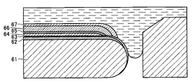
このように、毛細管力により液を上方向に持ち上げるためには、毛細管の水接触表面を撥水性にして、接触角を大きくする必要がある。図6に、撥水化処理を施した従来の多層レジスト膜を例示する。図6に示すように、基板61上に形成した被加工膜62自身をヘキサメチルジシラザン(hexamethyldisilazane)(以下、「HMDS」ともいう。)で気相シリル化し、HMDS処理領域63を形成することにより基板を撥水化し、ウェハの側面部(ベベル部)と天面の周縁部がHMDSにより撥水化されている。その後、下層有機膜層64、シリコン含有中間層65、感光性レジスト層66を形成する。つづいて、液浸の保護膜となる撥水性で現像液に可溶なトップコート層67を形成する。また、ウェハ外周近傍も撥水性で現像液に可溶なトップコート層67が最表面に露出して、毛細管力を高めている。図7に、撥水化処理を施した従来の単層レジスト膜を例示する。図7に示すように、基板71に形成した被加工膜72上に、HMDS処理領域73を形成することにより基板を撥水化する。その後、塗布型有機反射防止膜74、感光性レジスト層76を形成し、液浸の保護膜となる撥水性で現像液に可溶なトップコート層77を形成している。
しかし、このような従来の方法では、ベベル部の撥水性はHMDS処理レベルに止まり、水の接触角が60°程度であるため、撥水性が不足する場合がある。また、HMDSは、各種塗布膜を形成する前の被加工膜に対してのみ処理することができ、その処理はウェハ全面への処理が前提となるため、パターン形成に影響しない程度の撥水性しか付与できないという問題が有った。また、ウェハ外周部の撥水性を維持するために、ウェハ外周のレジストなどのエッジ除去に制限が入り、発塵対策に制約がかかるという問題があった。さらに、剥がれを抑制するために密着力を高められるのは、被加工膜とその直上の塗布膜のみであり、膜剥がれによるパターン欠陥抑制効果としては充分ではなく、液浸露光時に液浸液の対流でウェハエッジからの剥がれによる異物が浮遊しパターン欠陥を誘発するという問題があった。また、従来の撥水化処理においては、ウェハ全面における撥水性の処理は、露光工程において悪影響があるとの懸念があり、表面全体に好ましい撥水性を付与する方法は検討されていなかった。本発明の課題は、液浸露光において要求される撥水性が十分に高く、膜剥がれ抑制効果の大きいレジストパターンの形成方法と、その方法により製造した半導体デバイスを提供することにある。 However, in such a conventional method, the water repellency of the bevel portion remains at the HMDS treatment level, and the water contact angle is about 60 °, so that the water repellency may be insufficient. In addition, HMDS can process only the film to be processed before forming various coating films, and the process is premised on the entire surface of the wafer. There was a problem that it could not be granted. In addition, in order to maintain the water repellency of the outer peripheral portion of the wafer, there is a problem that the removal of the edge of the resist on the outer periphery of the wafer is restricted and the countermeasure against dust generation is restricted. Furthermore, in order to suppress peeling, only the film to be processed and the coating film immediately above the film can be improved.This is not sufficient as a pattern defect suppression effect due to film peeling, and the immersion liquid is not effective during immersion exposure. There has been a problem that foreign matter floats due to peeling from the wafer edge due to convection and induces pattern defects. Further, in the conventional water repellency treatment, there is a concern that the water repellency treatment on the entire surface of the wafer has an adverse effect in the exposure process, and a method for imparting preferable water repellency to the entire surface has not been studied. An object of the present invention is to provide a method for forming a resist pattern having a sufficiently high water repellency required in immersion exposure and having a large effect of suppressing film peeling, and a semiconductor device manufactured by the method.
本発明のある実施形態によれば、被加工膜が形成された半導体デバイスの基板上に対物レンズを配置し、対物レンズと基板の間に液膜を形成して露光する液浸露光によるレジストパターンの形成方法であって、少なくとも撥水化剤と溶剤とからなる撥水化剤薬液で処理した基板を露光することを特徴とするレジストパターンの形成方法を提供する。また、本発明の別の実施形態によれば、かかるレジストパターンの形成方法により製造した半導体デバイスが提供される。 According to an embodiment of the present invention, a resist pattern by immersion exposure in which an objective lens is disposed on a substrate of a semiconductor device on which a film to be processed is formed, and a liquid film is formed between the objective lens and the substrate for exposure. The method of forming a resist pattern is characterized in that a substrate treated with a water repellent chemical solution comprising at least a water repellent and a solvent is exposed. Moreover, according to another embodiment of the present invention, a semiconductor device manufactured by such a resist pattern forming method is provided.
本発明の実施形態によれば、基板を強力に撥水化するため、強い毛細管力により液浸液のこぼれを抑制する効果を高めることができる。 According to the embodiment of the present invention, since the substrate is strongly water-repellent, it is possible to enhance the effect of suppressing immersion liquid spillage by a strong capillary force.
本発明のレジストパターンの形成方法は、液浸露光によるレジストパターンの形成方法において少なくとも撥水化剤と溶剤とからなる撥水化剤薬液で処理した基板を露光することを特徴とする。ウェハを液状の上記撥水化剤薬液で処理することにより、強力に撥水化することができるため、強い毛細管力により液浸液のこぼれを抑制する効果を高めることができる。従来のHMDS処理では、水の接触角は60°程度に止まり、パターン形成に影響を与えない程度の撥水性しか得られなかったが、本発明によれば、水の接触角が80°程度またはそれ以上に及ぶ強力な撥水化処理が可能である。したがって、本発明のレジストパターンの形成方法により、メニスカスの崩壊と基板裏面の汚染が防止されるため、ウェハ裏面の異物によるデフォーカスに起因するパターン欠陥のない高品質の半導体デバイスを提供することができる。液浸リソグラフィーにおいて、感光性レジスト層上に液浸液からの有機汚染を防止するために現像液に可溶なトップコート層を形成する場合がある。現像液に可溶なトップコート層は、一般に撥水性であるため、トップコート層が最表面を覆う構造になっているときは、比較的ウェハ周縁部における液浸露光時の液こぼれに対しては有利であるが、コストなどの観点から現像液に可溶なトップコート層を使用しない場合は、本発明の撥水化処理方法が特に有効である。 The resist pattern forming method of the present invention is characterized by exposing a substrate treated with a water repellent chemical solution comprising at least a water repellent agent and a solvent in a resist pattern forming method by immersion exposure. By treating the wafer with the liquid water repellent chemical, the water can be made strongly water repellent, so that the effect of suppressing spillage of the immersion liquid can be enhanced by a strong capillary force. In the conventional HMDS treatment, the water contact angle is only about 60 °, and only water repellency that does not affect pattern formation can be obtained, but according to the present invention, the water contact angle is about 80 ° or More powerful water repellent treatment is possible. Therefore, the resist pattern forming method of the present invention prevents the meniscus from collapsing and the contamination of the backside of the substrate, so that it is possible to provide a high-quality semiconductor device free from pattern defects caused by defocusing due to foreign matter on the backside of the wafer. it can. In immersion lithography, a top coat layer that is soluble in a developer may be formed on the photosensitive resist layer in order to prevent organic contamination from the immersion liquid. Since the top coat layer soluble in the developer is generally water-repellent, when the top coat layer is structured to cover the outermost surface, it is relatively free from liquid spills during immersion exposure at the wafer periphery. Is advantageous, but the water repellent treatment method of the present invention is particularly effective when a topcoat layer soluble in a developer is not used from the viewpoint of cost and the like.
また、撥水化処理がレジストの塗布性能などに影響を与え、パターン形成に悪影響を及ぼす場合には、半導体チップが得られない欠けショットが生じるウェハの外周部のみを選択的に撥水化処理する必要がある。本発明の方法は、撥水化処理に用いる薬品が液状であるため、ウェハの外周部にのみ撥水化処理剤を吹き付けるなどして、ウェハの外周部のみを選択的に撥水化処理することが可能である。また、パターニングに影響しないウェハの外周部への処理であるため、水の接触角を80°程度またはそれ以上の強力な撥水化処理が可能である。ウェハの外周部は、発塵対策としてエッジ除去が施されることが多く、多層レジストプロセスでは様々なエッジ除去形状がプロセスの都合により必要となる場合がある。従来の方法では、任意にエッジ除去をすると最表面に親水性表面が露出する場合があるため、エッジ除去の自由度が低かった。しかし、本発明では、半導体製品を製造できないウェハの外周部のみに選択的に撥水化処理剤を吹き付けて接触させることにより、あらゆるエッジ除去形状に対し、最表面を撥水性にすることができる。 In addition, when the water repellency treatment affects the resist coating performance, etc., and adversely affects pattern formation, the water repellency treatment is selectively performed only on the outer periphery of the wafer where a chip shot is generated where a semiconductor chip cannot be obtained. There is a need to. In the method of the present invention, since the chemical used for the water repellent treatment is liquid, only the outer peripheral portion of the wafer is selectively water repellent treated by spraying a water repellent treatment agent only on the outer peripheral portion of the wafer. It is possible. Further, since the process is performed on the outer peripheral portion of the wafer that does not affect the patterning, a strong water repellent process with a water contact angle of about 80 ° or more is possible. Edge removal is often performed on the outer peripheral portion of the wafer as a measure against dust generation, and various edge removal shapes may be required for the convenience of the multi-layer resist process. In the conventional method, since the hydrophilic surface may be exposed on the outermost surface when the edge is arbitrarily removed, the degree of freedom of edge removal is low. However, in the present invention, the outermost surface can be made water-repellent with respect to all edge removal shapes by selectively spraying and contacting the water-repellent treatment agent only to the outer peripheral portion of the wafer where the semiconductor product cannot be manufactured. .
上記基板上に、下層有機膜層と、シリコン含有中間層と、感光性レジスト層とを形成する場合は、上記基板上にこれらの層をスピンコートする工程を含む多層レジスト法により形成することが好ましく、少なくとも各スピンコートの間、最初のスピンコートの前、および最後のスピンコートの後のいずれかにに、撥水化剤薬液で処理する態様が好ましい。かかる態様によれば、従来のように、被加工膜とその直上の下層有機膜層との間のみの密着力を高める態様と異なり、多層レジスト構造の各膜間の密着力を向上させることができる。また、パターン形成領域に影響を与えず、液浸露光時に剥がれやすく、密着力が要求されるウェハ外周部のみに選択的にシランカップリング剤などの撥水化剤薬液による処理を施すことにより、剥がれを抑制することが可能である。撥水化剤としてシランカップリング剤を用いる場合は、密着強化の効果が得られる。同様に、基板と基板上に形成する感光性レジスト層との密着力を高める点と、感光性レジスト層と感光性レジスト層上に形成するトップコート層との密着力を高める点と、液浸露光時の剥がれを抑える点で、感光性レジスト層を基板上にスピンコートする工程を含むフォトリソグラフィ工程により好ましく、このフォトリソグラフィ工程において、少なくとも前記各スピンコートの間、最初のスピンコートの前、および最後のスピンコートの後のいずれかに、シランカップリング剤などを含む撥水化剤薬液で処理する態様が好ましい。 When forming a lower organic film layer, a silicon-containing intermediate layer, and a photosensitive resist layer on the substrate, it may be formed by a multilayer resist method including a step of spin-coating these layers on the substrate. Preferably, a mode in which the treatment with the water repellent chemical is performed at least between each spin coat, before the first spin coat, and after the last spin coat is preferable. According to such an aspect, unlike the conventional aspect in which the adhesion between the film to be processed and the lower organic film layer immediately above it is increased, the adhesion between each film of the multilayer resist structure can be improved. it can. In addition, it does not affect the pattern formation area, is easily peeled off during immersion exposure, and is selectively treated only with a water repellent chemical such as a silane coupling agent only on the wafer outer periphery where adhesion is required. It is possible to suppress peeling. When a silane coupling agent is used as the water repellent agent, an effect of enhancing adhesion can be obtained. Similarly, increasing the adhesion between the substrate and the photosensitive resist layer formed on the substrate, increasing the adhesion between the photosensitive resist layer and the topcoat layer formed on the photosensitive resist layer, It is preferable to use a photolithography process including a step of spin-coating a photosensitive resist layer on a substrate in terms of suppressing peeling at the time of exposure. In this photolithography step, at least during each of the spin coatings, before the first spin coating, And after either the last spin coating, an embodiment in which treatment with a water repellent chemical containing a silane coupling agent or the like is preferred.
レジストパターンを形成するための微細加工用レジスト膜の下に形成する被加工膜は特に限定されるものではなく、通常、ポリシリコン、シリコン酸化膜、シリコン窒化膜、CVD形成アモルファスカーボン膜などの無機膜、ないしその上に下層無機の反射防止膜が形成された膜である。撥水化処理は、上記微細加工用レジスト膜の下地層である被加工膜表面、基板上に形成される下層有機膜層、シリコン含有中間層、および感光性レジスト層の積層により構成される膜のうち、液浸露光時に水と接触する最表面に対して実施する。また、撥水化処理は、気相処理ではなく、撥水化剤薬液による液体の吹き付け、または浸漬することにより処理し、処理表面に撥水性を付与するものである。また、撥水化剤薬液としてシランカップリング剤を含む薬液による処理(密着強化処理)は、撥水化処理と同様に行なうことができ、密着性を付与することができる。 The film to be formed under the fine processing resist film for forming the resist pattern is not particularly limited and is usually inorganic such as polysilicon, silicon oxide film, silicon nitride film, CVD-formed amorphous carbon film, etc. It is a film or a film on which a lower layer inorganic antireflection film is formed. Water repellent treatment is a film composed of a laminate of a processed film surface, which is an underlayer of the above-described fine processing resist film, a lower organic film layer formed on the substrate, a silicon-containing intermediate layer, and a photosensitive resist layer. Of these, it is performed on the outermost surface that comes into contact with water during immersion exposure. Further, the water repellent treatment is not a vapor phase treatment, but is performed by spraying or immersing a liquid with a water repellent chemical, thereby imparting water repellency to the treated surface. Moreover, the process (adhesion reinforcement | strengthening process) by the chemical | medical solution containing a silane coupling agent as a water repellent chemical | medical solution can be performed similarly to a water repellent process, and can provide adhesiveness.
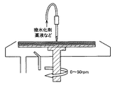
撥水化処理は、たとえば図4に示す装置により、1種以上の撥水化剤を含む撥水化剤薬液からなる処理薬液をパドルし、液膜を形成することでウェハ全面に施すことも可能である。この際は、ウェハの回転数は静止(0rpm)を基本とし、数秒間隔で50rpmの揺動を与え、液を攪拌することも可能である。しかしながら、ウェハ全面への処理を施す場合、後の工程で塗布される微細加工用レジスト膜の被パターニング部分を撥水化することになるため、塗布性能、現像性能、多層プロセスドライ現像性能への悪影響の懸念などから撥水化処理方法に制約がかかる。そのため、目的とする撥水性の付与が不充分になることが考えられる。そのような場合には、後述の撥水化剤として非フッ素系の撥水化剤であって、アルキル基およびエポキシ基の少なくともいずれかを構造中に含む撥水化剤を用いることが好ましく、また、撥水化剤薬液に、水、酸およびアルカリの少なくともいずれかを追加することにより撥水性の付与を十分なものとすることができる。ウェハ全面に対して撥水化処理を施した場合は、レジストのパターン倒れを抑制する効果をより改善することができる。図17にレジストパターンの概略図を示す。図17(a)は、膜厚(レジストのパターン高さ)H、線幅dのパターンの一例を示し、図17(b)は、パターン倒れを示す概略図であり、図17(c)は正常なパターンを示す概略図である。液浸露光にかかわらず、レジストパターンが微細化されるにつれて、アスペクト比、膜厚H/線幅dが高くなり、基板とレジストパターンの接触面積が小さくなるため、レジストのパターン倒れが起こりやすくなるという問題がある。本発明においては、上記のように撥水化剤を含む撥水化剤薬液を用いてウェハの全面を処理した場合に、基板とレジストとの密着性を向上させることが可能となり、その結果パターン倒れを抑制できることを見出した。したがってウェハ全面への撥水化処理に制約がかかる場合は、後述のようにウェハ外周部を局所的に処理することができるが、パターン倒れなどの問題を抑制するためには、ウェハの全面に撥水処理を施すことが望ましい。 The water repellent treatment may be performed on the entire surface of the wafer by padding a treatment chemical solution including a water repellent chemical solution containing one or more water repellent agents and forming a liquid film, for example, using the apparatus shown in FIG. Is possible. In this case, the rotation speed of the wafer is basically static (0 rpm), and the liquid can be agitated by giving a swing of 50 rpm at intervals of several seconds. However, when processing the entire surface of the wafer, the patterning portion of the resist film for microfabrication to be applied in a later step will be water repellent, so that the coating performance, development performance, and multilayer process dry development performance will be improved. The water repellent treatment method is restricted due to concerns about adverse effects. For this reason, it may be considered that the desired water repellency is insufficiently provided. In such a case, it is preferable to use a non-fluorine-based water repellent as the water repellent described later, and a water repellent containing at least one of an alkyl group and an epoxy group in the structure, Further, water repellency can be sufficiently imparted by adding at least one of water, acid and alkali to the water repellent chemical. When the water repellent treatment is performed on the entire wafer surface, the effect of suppressing the resist pattern collapse can be further improved. FIG. 17 shows a schematic diagram of a resist pattern. FIG. 17A shows an example of a pattern having a film thickness (resist pattern height) H and a line width d, FIG. 17B is a schematic diagram showing pattern collapse, and FIG. It is the schematic which shows a normal pattern. Regardless of immersion exposure, as the resist pattern is miniaturized, the aspect ratio and the film thickness H / line width d increase, and the contact area between the substrate and the resist pattern decreases, so that the resist pattern collapse easily occurs. There is a problem. In the present invention, when the entire surface of the wafer is treated with a water repellent chemical solution containing a water repellent as described above, it becomes possible to improve the adhesion between the substrate and the resist, resulting in a pattern. It was found that the collapse can be suppressed. Therefore, when the water repellency treatment on the entire surface of the wafer is restricted, the outer periphery of the wafer can be locally processed as described later. However, in order to suppress problems such as pattern collapse, the entire surface of the wafer is It is desirable to perform a water repellent treatment.
また、ウェハ全面への撥水化処理に制約がかかる場合には、被パターニング部分を除くウェハの側面と、天面の周縁部および底面の周縁部(これらをまとめて、以下、「外周部」ともいう。)のみに限定し、局所的に撥水化処理などをする方法がある。この方法は、図5に示すように、撥水化剤薬液などを、エッジリンス機構を用い、ウェハ外周部に局所的に処理する方法である。具体的には、ウェハを100rpm〜2000rpm程度で回転させながら、撥水化剤薬液などでウェハの天面の周縁部のみを選択的に処理し、液浸液の接触角を高めるものである。このとき周縁部の撥水化処理などの領域幅はノズル位置をステップモーターで高精度に位置制御することで、ウェハエッジから0.3mm〜3.0mm程度に調整することが可能である。このノズルは、既存技術でウェハエッジの塗布膜除去を行なうエッジリンスノズルをそのまま用いてもよく、エッジリンスと使い分けをする場合は、エッジリンスノズルを増設することで容易に行なうことができる。なお、塗布膜とは、下層有機膜、シリコン含有中間層、レジスト及び反射防止膜、トップコート等、所望のパターンを得るために一時的に基板上に形成する膜であり、最終的に半導体デバイスに膜として残らない膜をいう。また、被加工膜とは、上記塗布膜も含み、下層有機膜の下地となる基板部分(シリコン基板、酸化膜、窒化膜、Low−K膜等)を含めた膜のうち、最終的に半導体デバイスの形成膜として残る部材を包含するものである。 In addition, when the water repellency treatment on the entire wafer surface is restricted, the side surface of the wafer excluding the portion to be patterned, the peripheral edge portion of the top surface, and the peripheral edge portion of the bottom surface (collectively, hereinafter referred to as “peripheral portion”) There is also a method of locally performing a water repellent treatment. As shown in FIG. 5, this method is a method in which a water repellent chemical or the like is locally processed on the wafer outer peripheral portion using an edge rinse mechanism. Specifically, only the peripheral edge of the top surface of the wafer is selectively treated with a water repellent chemical solution while rotating the wafer at about 100 rpm to 2000 rpm to increase the contact angle of the immersion liquid. At this time, the area width of the water repellent treatment or the like at the peripheral edge can be adjusted to about 0.3 mm to 3.0 mm from the wafer edge by controlling the position of the nozzle with high accuracy by a step motor. As this nozzle, an edge rinse nozzle that removes the coating film on the wafer edge by an existing technique may be used as it is. When the nozzle is used separately from the edge rinse, it can be easily performed by adding an edge rinse nozzle. The coating film is a film temporarily formed on a substrate to obtain a desired pattern, such as a lower organic film, a silicon-containing intermediate layer, a resist and an antireflection film, and a top coat. A film that does not remain as a film. In addition, the film to be processed includes the above-described coating film, and finally the semiconductor among the films including the substrate portion (silicon substrate, oxide film, nitride film, Low-K film, etc.) that is the base of the lower organic film. It includes members that remain as device forming films.
ウェハの底面の周縁部に関しても、裏面側から撥水化剤薬液などを吹き付けることにより、底面の周縁部に撥水化処理などをすることができる。底面を撥水性にすることで、液浸露光時などに液浸液が底面に廻り込んで、露光機ステージ上の異物による影響を排除することができる。この裏面撥水化用のノズルも、既存技術の塗布膜除去を行なうバックリンスノズルをそのまま用いてもよく、バックリンスと使い分けをする場合はバックリンスノズルを増設することで容易に行なうことができる。撥水化処理などが必要なエリアは、毛細管力により水を持ち上げる力を生む部分であり、ウェハエッジの表面が水平でない部分の最表面である。最も毛細管力への影響が大きいのは、ステージの外周枠との距離が近いウェハ基材自体のベベル部分であるが、その内側の塗布膜の非水平部分も撥水化されることが望ましい。したがって、ウェハ中央部は撥水化する必要はなく、ウェハ外周部の所定の領域を撥水化すればよい。 With respect to the peripheral portion of the bottom surface of the wafer, water repellent treatment or the like can be performed on the peripheral portion of the bottom surface by spraying a water repellent chemical or the like from the back surface side. By making the bottom surface water-repellent, the immersion liquid can reach the bottom surface during immersion exposure and the influence of foreign matter on the exposure machine stage can be eliminated. As the nozzle for water repellency on the back surface, the back rinse nozzle for removing the coating film of the existing technology may be used as it is, and when using separately from the back rinse, it can be easily performed by adding a back rinse nozzle. . The area where water repellent treatment or the like is necessary is a portion that generates a force to lift water by capillary force, and is the outermost surface of the portion where the surface of the wafer edge is not horizontal. The influence on the capillary force is the greatest in the bevel portion of the wafer substrate itself, which is close to the outer peripheral frame of the stage, but it is desirable that the non-horizontal portion of the coating film on the inside is also water repellent. Therefore, it is not necessary to make the wafer central portion water repellent, and it is only necessary to make a predetermined region of the wafer outer peripheral portion water repellent.
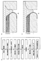
撥水化処理は、塗布機のエッジリンス機構を利用して行なうため、撥水化領域はエッジリンスの位置決め精度(0.2mm〜0.3mm程度)で最小値が決定される。また、最大値は図8(b)のウェハエッジの拡大図に見られるように、エッジ露光ショットの中の有効なチップ(○印)が減らない程度の値とする。通常の場合、以下に記載の様々なプロセスの事情により、レジストのエッジリンス除去幅が約3.0mm程度にまで及ぶことがあり、その場合は、3.0mmまで撥水化処理しても製品歩留まりに影響は出ないため、有効なチップが減らない程度の値とはエッジリンスの最大除去幅である。この時、撥水化処理は、微細加工用レジスト膜を形成する前または後の基板表面に実施する。また、微細加工用レジスト膜が多層構造を持つ場合は、多層膜スタックの各層塗布形成前後の任意の表面に処理することが可能である。撥水化処理に用いられる撥水化剤と基板との反応は、常温時に反応するものを選択することが好ましいが、反応性が悪い撥水化剤の場合、撥水化剤薬液を表面に接触させた後に、ホットプレート(熱板)などにより、60℃〜120℃の温度で1分程度の熱処理を施すこともでき、110℃〜150℃程度の熱処理を施すことが好ましい。熱処理の温度が低すぎると撥水化剤と基板との反応性を補助できない場合がある。また、熱処理の温度が高すぎると基板上に存在する積層膜の性質を変化させてしまう場合があるので、好ましくない。 Since the water repellent treatment is performed using the edge rinse mechanism of the coating machine, the minimum value of the water repellent area is determined by the edge rinse positioning accuracy (about 0.2 mm to 0.3 mm). Further, as shown in the enlarged view of the wafer edge in FIG. 8B, the maximum value is set to such a value that the effective chips (◯ marks) in the edge exposure shot are not reduced. Normally, due to various processes described below, the edge rinse removal width of the resist may reach up to about 3.0 mm. In that case, even if water repellent treatment is performed up to 3.0 mm, the product Since the yield is not affected, the value that does not reduce the number of effective chips is the maximum edge rinse removal width. At this time, the water repellent treatment is performed on the substrate surface before or after the formation of the fine processing resist film. When the resist film for microfabrication has a multilayer structure, it can be processed on an arbitrary surface before and after application of each layer of the multilayer film stack. For the reaction between the water repellent used in the water repellent treatment and the substrate, it is preferable to select one that reacts at room temperature, but in the case of a water repellant with poor reactivity, a water repellent chemical solution is applied to the surface. After the contact, heat treatment can be performed at a temperature of 60 ° C. to 120 ° C. for about 1 minute using a hot plate (hot plate) or the like, and it is preferable to perform a heat treatment of about 110 ° C. to 150 ° C. If the temperature of the heat treatment is too low, the reactivity between the water repellent and the substrate may not be assisted. In addition, if the temperature of the heat treatment is too high, the properties of the laminated film existing on the substrate may be changed, which is not preferable.
撥水化剤としては、フッ素系撥水化剤、シリコーン系撥水化剤、フッ素・シリコーン系撥水化剤、シランカップリング剤、シリル化剤、アルキル化剤またはアシル化剤を用いることができる。これらは1種または2種以上を混合して用いてもよい。いずれの場合も、各撥水化剤に適した溶剤に、0.5質量%〜5.0質量%に希釈したものを用いる。撥水化剤としては、下記の式(1)と式(2)で示されるものが例として挙げられる。なお、撥水化剤の加水分解を避けるため、使用する溶剤は、蒸留処理、吸収剤の利用または水分除去フィルタの利用により脱水し、水分を好ましくは50ppm以下、より好ましくは30ppm以下とする。なお、水分量は、カールフィッシャー法によって確認することができる。 As the water repellent, a fluorine water repellent, a silicone water repellent, a fluorine / silicone water repellent, a silane coupling agent, a silylating agent, an alkylating agent or an acylating agent may be used. it can. You may use these 1 type or in mixture of 2 or more types. In either case, a solvent suitable for each water repellent agent is diluted to 0.5% by mass to 5.0% by mass. Examples of the water repellent agent include those represented by the following formulas (1) and (2). In order to avoid hydrolysis of the water repellent, the solvent to be used is dehydrated by distillation treatment, use of an absorbent, or use of a water removal filter, and the water content is preferably 50 ppm or less, more preferably 30 ppm or less. The water content can be confirmed by the Karl Fischer method.
フッ素系撥水化剤、シリコーン系撥水化剤、フッ素・シリコーン系撥水化剤としては、以下のものを例示することができる。 Examples of the fluorine water repellent, the silicone water repellent, and the fluorine / silicone water repellent include the following.

(式(1)中、R1,R2,R3は、H,CH3,C2H5またはC3H7
nは、0〜5の整数
Rは、CmF2m+1 または、CmH2m+1 であり、mは、1〜10の整数である。)
(In the formula (1), R 1 , R 2 and R 3 are H, CH 3 , C 2 H 5 or C 3 H 7.
n is an integer R of 0~5, C m F 2m + 1 or a C m H 2m + 1, m is an integer from 1 to 10. )
(式(2)中、R1,R2,R3は、(CH2)n−CmF2m+1 であり、nは、0〜5の整数であり、mは、1〜10の整数
R0は、H,CkH2k+1,Si(OCH3)3,Si(OC2H5)3,Si(OC3H7)3、又は、NH結合の右側の構造(SiR1R2R3)と同一構造であり、kは、1〜3の整数である。)
ウェハ全面の撥水化処理を行なう場合は、フッ素系撥水剤の場合は、ウェハとの相互作用が十分ではなく、パターン倒れの抑制が不足することがあるが、アルキル基やエポキシ基を含有する上記式(2)で示される化合物を撥水剤として用いた場合には、密着力が向上し、HMDSなどを用いた従来の処理に比べて密着力を向上させることができ、その結果パターン倒れを抑制する効果が著しく改善される。上記式(2)のなかでも、末端がアミノ基であるこが好ましい。
(In the
When water repellent treatment is performed on the entire surface of the wafer, the fluorine-based water repellent does not have sufficient interaction with the wafer and may not be sufficient to suppress pattern collapse, but contains alkyl groups or epoxy groups. When the compound represented by the above formula (2) is used as a water repellent, the adhesion is improved and the adhesion can be improved as compared with the conventional treatment using HMDS. As a result, the pattern The effect of suppressing the collapse is remarkably improved. Among the above formulas (2), the terminal is preferably an amino group.
撥水化剤として、シリル化剤を用いることもできる。シリル化剤としては、たとえば、BSA(N,O-bis(trimethylsilyl)acetamide),BSTFA(N,O-bis(trimethylsilyl)trifluoroacetamide),HMDS(hexamethyldisilazane),MSTFA(N-methyl-N-trimethylsilyl-trifluoroacetamide),TMCS(trimethylchlorosilane),TMSI(N-trimethylsilylimidazole),DMSDMA(dimethylsilyldimethylamine)などが用いられる。 A silylating agent can also be used as the water repellent. Examples of the silylating agent include BSA (N, O-bis (trimethylsilyl) acetamide), BSTFA (N, O-bis (trimethylsilyl) trifluoroacetamide), HMDS (hexamethyldisilazane), MSTFA (N-methyl-N-trimethylsilyl-trifluoroacetamide). ), TMCS (trimethylchlorosilane), TMSI (N-trimethylsilylimidazole), DMSDMA (dimethylsilyldimethylamine), and the like.
密着強化効果のある撥水化剤としては、主にシランカップリング剤を用いることができる。また、シランカップリング剤の中には、撥水化処理性能を示すものもある。撥水化処理性能の高いものとしては、プロポキシシラン誘導体が水中での加水分解が遅く有効である。シランカップリング剤には、ビニルトリクロルシラン,ビニルトリメトキシシラン,ビニルトリエトキシシラン,2-(3、4-エポキシシクロヘキシル)エチルトリメトキシシラン,3-グリシドキシプロピルトリメトキシシラン,3-グリシドキシプロピルメチルジエトキシシラン,3-グリシドキシプロピルトリエトキシシラン,p-スチリルトリメトキシシラン,3-メタクリロキシプロピルメチルジメトキシシラン,3-メタクリロキシプロピルトリメトキシシラン,3-メタクリロキシプロピルメチルジエトキシシラン,3-メタクリロキシプロピルトリエトキシシラン,3-アクリロキシプロピルトリメトキシシラン,(アミノエチル)3-アミノプロピルメチルジメトキシシラン,N-2(アミノエチル)3-アミノプロピルトリメトキシシラン,N-2(アミノエチル)3-アミノプロピルトリエトキシシラン,3-アミノプロピルトリメトキシシラン,3-アミノプロピルトリエトキシシラン,3-トリエトキシシリル-N-(1、3-ジメチル-ブチリデン)プロピルアミン,N-フェニル-3-アミノプロピルトリメトキシシラン,N-(ビニルベンジル)-2-アミノエチル-3-アミノプロピルトリメトキシシラン3-ウレイドプロピルトリエトキシシラン,3-クロロプロピルトリメトキシシラン,3-メルカプトプロピルメチルジメトキシシラン,3-メルカプトプロピルトリメトキシシラン,ビス(トリエトキシシリルプロピル)テトラスルフィド,3-イソシアネートプロピルトリエトキシシランなどがあり、これらの中でもメトキシシラン、エトキシシランをプロピオキシシランに置き換えたものが撥水化剤としては有効である。密着強化処理では、反応性が高いメトキシシラン誘導体が好ましい。なお、シランカップリング剤を含む撥水化剤薬液の加水分解を避けるため、使用する溶剤は、蒸留処理、吸収剤の利用または水分除去フィルタの利用により脱水し、水分を好ましくは50ppm以下、より好ましくは30ppm以下とする。 A silane coupling agent can be mainly used as a water repellent agent having an adhesion strengthening effect. Some silane coupling agents exhibit water repellency treatment performance. As a high water repellency treatment performance, a propoxysilane derivative is effective because of its slow hydrolysis in water. Silane coupling agents include vinyltrichlorosilane, vinyltrimethoxysilane, vinyltriethoxysilane, 2- (3,4-epoxycyclohexyl) ethyltrimethoxysilane, 3-glycidoxypropyltrimethoxysilane, 3-glycid. Xylpropylmethyldiethoxysilane, 3-glycidoxypropyltriethoxysilane, p-styryltrimethoxysilane, 3-methacryloxypropylmethyldimethoxysilane, 3-methacryloxypropyltrimethoxysilane, 3-methacryloxypropylmethyldiethoxy Silane, 3-methacryloxypropyltriethoxysilane, 3-acryloxypropyltrimethoxysilane, (aminoethyl) 3-aminopropylmethyldimethoxysilane, N-2 (aminoethyl) 3-aminopropyltrimethoxysilane, N-2 (aminoethyl) 3-aminopropyltriethoxysilane, 3-aminopropyltrimethoxysilane, 3-aminopropyltriethoxysilane, 3-triethoxysilyl-N- (1,3-dimethyl-butylidene) propylamine , N-phenyl-3-aminopropyltrimethoxysilane, N- (vinylbenzyl) -2-aminoethyl-3-aminopropyltrimethoxysilane 3-ureidopropyltriethoxysilane, 3-chloropropyltrimethoxysilane, 3- Mercaptopropylmethyldimethoxysilane, 3-mercaptopropyltrimethoxysilane, bis (triethoxysilylpropyl) tetrasulfide, 3-isocyanatopropyltriethoxysilane, etc. Among them, methoxysilane and ethoxysilane were replaced with propoxyoxysilane thing Is effective as a water repellent. In the adhesion strengthening treatment, a highly reactive methoxysilane derivative is preferable. In order to avoid hydrolysis of the water repellent chemical solution containing the silane coupling agent, the solvent used is dehydrated by distillation treatment, use of an absorbent or use of a water removal filter, and moisture is preferably 50 ppm or less. Preferably it is 30 ppm or less.
アルキル化剤としては、ペンタフルオロベンジルブロマイド、1,4,7,10,13,16-ヘキサオキサシクロオクタデカンなどが用いられる。また、アシル化剤としては、PFPA(ペンタフルオロプロピオン酸無水物)、HFBA(無水ヘプタフルオロ酪酸)、無水酢酸などが用いられる。被撥水化処理面が、多層レジストに用いる下層有機膜層、感光性レジスト層などの有機膜の場合は、下記の式(3)または式(4)ような構造の化合物を、有機膜を溶解しない溶剤に0.5質量%〜5.0質量%の割合で溶解した撥水化剤薬液を用いることが望ましい。 As the alkylating agent, pentafluorobenzyl bromide, 1,4,7,10,13,16-hexaoxacyclooctadecane or the like is used. As the acylating agent, PFPA (pentafluoropropionic anhydride), HFBA (anhydrous heptafluorobutyric acid), acetic anhydride, or the like is used. When the water-repellent treatment surface is an organic film such as a lower organic film layer or a photosensitive resist layer used for a multilayer resist, a compound having a structure as shown in the following formula (3) or formula (4) is used: It is desirable to use a water repellent chemical solution dissolved in a ratio of 0.5 mass% to 5.0 mass% in a solvent that does not dissolve.
(式(3)中、R1,R2,R3は、メトキシ基、エトキシ基、プロピオキシ基またはアセトキシ基
nは、0〜5の整数
官能基Yは、ビニル基、エポキシ基、メタクリル基、アミノ基、メルカプト基、スチリル基、アクリロキシ基、ウレイド基、クロロプロピル基、スルフィド基、イソシアネート基またはアルコキシ基である。)
(In the formula (3), R 1 , R 2 and R 3 are a methoxy group, an ethoxy group, a propoxy group or an acetoxy group n, an integer functional group Y of 0 to 5, a vinyl group, an epoxy group, a methacryl group, (Amino group, mercapto group, styryl group, acryloxy group, ureido group, chloropropyl group, sulfide group, isocyanate group or alkoxy group)
![]()
![]()
(式(4)中、Rは、CmF2m+1 またはCmH2m+1であり、mは、1〜10の整数
nは、0〜5の整数
官能基Yは、ビニル基、エポキシ基、メタクリル基、アミノ基、メルカプト基、スチリル基、アクリロキシ基、ウレイド基、クロロプロピル基、スルフィド基、イソシアネート基またはアルコキシ基である。)
以上の内容に基づき、被処理素材である無機膜と有機膜に分けて、撥水化剤の好ましい組合わせを例示すると表1のようになる。一方、多層レジスト層を溶解する溶剤、多層レジスト層を溶解しない溶剤と現像液に可溶なトップコート層も溶解しない溶剤に分類して、使用が好ましい溶剤を例示すると、表2のようになる。また、エッジリンスと同時に処理し、露出基板に対して処理する場合には、熱硬化前の塗布膜を溶解する溶剤を選択するのが好ましい。さらに、塗布膜を被処理膜とし、エッジリンスしない場合には、塗布膜を溶解しない溶剤を選択する態様が好ましい。一方、処理直後に、塗布後の熱処理が入る場合には、シランカップリング剤としては、加水分解性を落とし、疎水性を向上する点で、エトキシシラノール誘導体またはプロピオキシシラノール誘導体が好ましい。しかし、処理直後に熱処理ではなく、塗布処理が入る場合には、常温で反応するメトキシシラノール誘導体が好ましい。撥水化剤の撥水性と密着強化と両方の効果を1種類の薬液で得る場合は、式(1)に示す構造の撥水化剤と、中庸な反応性のエトキシシラノール系のシランカップリング剤の混合液を使用するのが好適である。また、式(2)に示す構造の撥水化剤と、シリル化剤として使用するシラザン系の化合物は、副生成物としてアンモニアを発生するため、パターンニングに留意する必要がある。さらに、上記のように2種以上の撥水化剤を混合して用いる態様は、種々の基板への反応性を確保することで汎用性の高い撥水・密着強化材料とできる点で好ましい。
(In the formula (4), R is C m F 2m + 1 or C m H 2m + 1, m is an integer n of 1 to 10, an integer functional group Y of 0 to 5, a vinyl group, (Epoxy group, methacryl group, amino group, mercapto group, styryl group, acryloxy group, ureido group, chloropropyl group, sulfide group, isocyanate group or alkoxy group)
Based on the above contents, a preferable combination of water repellent agents is illustrated in Table 1 by dividing into an inorganic film and an organic film which are materials to be processed. On the other hand, a solvent that dissolves the multilayer resist layer, a solvent that does not dissolve the multilayer resist layer, and a solvent that does not dissolve the top coat layer that is soluble in the developer, and examples of solvents that are preferably used are shown in Table 2. . Moreover, when processing with edge rinse and processing with respect to an exposed substrate, it is preferable to select the solvent which melt | dissolves the coating film before thermosetting. Furthermore, when the coating film is a film to be processed and edge rinsing is not performed, a mode in which a solvent that does not dissolve the coating film is selected is preferable. On the other hand, when a heat treatment after coating is performed immediately after the treatment, the silane coupling agent is preferably an ethoxysilanol derivative or a propoxysilanol derivative in terms of reducing hydrolyzability and improving hydrophobicity. However, a methoxysilanol derivative that reacts at room temperature is preferred when a coating treatment is performed immediately after the treatment, rather than a heat treatment. When both water repellency and adhesion strengthening effects of a water repellent are obtained with a single chemical, the water repellent with the structure shown in formula (1) and a moderately reactive ethoxysilanol-based silane coupling It is preferred to use a mixture of agents. In addition, since the water repellent having the structure shown in Formula (2) and the silazane compound used as the silylating agent generate ammonia as a by-product, it is necessary to pay attention to patterning. Furthermore, the mode of using a mixture of two or more water repellents as described above is preferable in that a highly versatile water repellent / adhesion reinforcing material can be obtained by ensuring reactivity to various substrates.
本発明の撥水化処理の典型例を図1と図9〜図13に示す。基本的には、シランカップリング剤を含む密着性を強化する効果のある撥水化剤薬液による処理は、上層と下層の密着性が低い膜の間で行ない、シランカップリング剤を含まない撥水化剤薬液による撥水化処理は、全ての層の形成後に行なうのが好ましい。しかしながら、後続の露光プロセス、エッチング、拡散または注入などにおける剥がれ、クランピングなどによる物理的接触による発塵、膜特性自体による剥がれなどにより発塵が生じる可能性がある。そして、これらの様々なプロセスの事情により、レジストのエッジ部分における下層有機膜層、シリコン含有中間層、感光性レジスト層、現像液に可溶なトップコート層の除去の必要性が決まる。したがって、プロセスフローにはバリエーションが必要であり、下記実施例は処理フローの一例であり、事情により多数のバリエーションが考えられる。 A typical example of the water repellent treatment of the present invention is shown in FIGS. 1 and 9 to 13. Basically, the treatment with a water repellent chemical solution that has an effect of strengthening the adhesion including the silane coupling agent is performed between the films having low adhesion between the upper layer and the lower layer, and does not contain the silane coupling agent. The water repellency treatment with the hydrating agent chemical is preferably performed after the formation of all layers. However, there is a possibility of dust generation due to peeling in subsequent exposure processes, etching, diffusion or implantation, dust generation due to physical contact by clamping, etc., peeling due to film characteristics itself, and the like. The circumstances of these various processes determine the necessity of removing the lower organic film layer, the silicon-containing intermediate layer, the photosensitive resist layer, and the top coat layer soluble in the developer at the edge portion of the resist. Therefore, variations are necessary for the process flow, and the following embodiment is an example of the processing flow, and many variations are conceivable depending on circumstances.
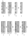
図1は、トップコート層が最表面を覆う場合の例であり、図1(a)にプロセスフローを示し、図1(b)に処理後のウェハ外周部の断面構造を示す。図1(b)に示すように、基板1上に、被加工膜2を形成した後、本発明における撥水化剤薬液からなる撥水化処理層3を形成し、その後、塗布型有機反射防止膜4、感光性レジスト層6、トップコート層7を形成する。被撥水化処理表面は、一般に無機膜であり、撥水化処理剤は、式(1)、式(2)またはシリル化剤、シランカップリング剤を用いることが望ましい。また、いずれの化合物も溶剤に0.5質量%〜5.0質量%に希釈して用いるが、使用する溶剤は、アルコール系、アセテート系、ケトン系、水系、芳香族系など特に制約なく、化合物の溶解安定性の高いものを使用することができる。被撥水化処理表面が有機膜の場合は、式(3)またはプロピオキシシラノールまたはエトキシシラノールを含むシランカップリング剤を用いることが望ましい。基板上に撥水化剤薬液を供給すると、基板表面に撥水化剤が吸着し、化学反応により撥水化剤の単分子層が形成されるため、基板とステージ外周部9との間における液浸液のこぼれを回避することができる。液浸露光が完了した後、感光性レジスト現像工程、エッチング工程の後、レジストを除去するために酸素プラズマによるアッシングおよび硫酸と過酸化水素水混合液を用いたウェット処理を実施する。このウェット処理を実施した際に、表面および裏面に形成された撥水化処理層3は剥離される。
FIG. 1 shows an example in which a top coat layer covers the outermost surface. FIG. 1 (a) shows a process flow, and FIG. 1 (b) shows a cross-sectional structure of a wafer outer peripheral portion after processing. As shown in FIG.1 (b), after forming the to-be-processed film |
図9は、トップコート層を形成しない場合の例であり、図9(a)にプロセスフローを示し、図9(b)と図9(c)に処理後のウェハ外周部の断面構造を示す。まず、基板1上に、被加工膜2、塗布型有機反射防止膜4、感光性レジスト層6を形成した後、撥水化処理層3を形成する。被撥水化処理表面は、無機膜と有機膜が混在しているため、撥水化剤は、式(1)、式(2)と式(3)の混合溶液またはプロピオキシシラノールまたはエトキシシラノールを含むシランカップリング剤を用いることが望ましい。また、いずれの化合物も溶剤に0.5質量%〜5.0質量%に希釈して用いるが、使用する溶剤はブチルアルコール以上の高級アルコール、ブチルエーテル以上の高級アルキルエーテル、水系などの中から感光性レジストを溶解しない溶剤を選択する。撥水化処理層3はレジスト除去工程で剥離される。また、図9(b)の例では、撥水化処理層3が、基板の側面と、基板の天面の周縁部と、基板の底面の周縁部に形成されている。また、図9(c)に示す例では、撥水化処理層3が、基板の側面と、基板の天面と、基板の底面の周縁部に形成されている。
FIG. 9 shows an example in which the top coat layer is not formed. FIG. 9A shows a process flow, and FIGS. 9B and 9C show a cross-sectional structure of the wafer outer peripheral portion after processing. . First, the
図10は、トップコート層を形成し、エッジリンスと撥水化処理を同時に施す場合の例であり、図10(a)にプロセスフローを示し、図10(b)に処理後のウェハ外周部の断面構造を示す。図10(b)に示すように、基板1上に、被加工膜2、塗布型有機反射防止膜4、感光性レジスト層6、トップコート層7を形成した後、トップコートエッジリンスを行ない、撥水化処理層3を形成する。被撥水化処理表面は、無機膜と有機膜が混在しているため、撥水化剤は、式(1)、式(2)と式(3)の混合溶液またはプロピオキシシラノールまたはエトキシシラノールを含むシランカップリング剤を用いることが望ましい。また、いずれの化合物も、溶剤に0.5質量%〜5.0質量%に希釈して用いる。使用する溶剤は、現像液に可溶なトップコートの溶剤に用いられるブチルアルコール以上の高級アルコール、ブチルエーテル以上の高級アルキルエーテルなどの中から選択し、現像液に可溶なトップコート層を溶解し、感光性レジストを溶解しない溶剤を選択する。撥水化処理層3は、レジスト除去工程で剥離される。
FIG. 10 shows an example in which a top coat layer is formed and edge rinse and water repellency treatment are simultaneously performed. FIG. 10A shows a process flow, and FIG. The cross-sectional structure of is shown. As shown in FIG. 10 (b), after forming the
図11は、トップコート層を形成することなく、エッジリンスと撥水化処理を同時に施す場合の例であり、図11(a)にプロセスフローを示し、図11(b)に処理後のウェハ外周部の断面構造を示す。図11(b)に示すように、基板1上に、被加工膜2、塗布型有機反射防止膜4、感光性レジスト層6を形成した後、エッジリンスを行ない、撥水化処理層3を形成する。被撥水化処理表面は、無機膜と有機膜が混在しているため、撥水化剤は、式(1)、式(2)と式(3)の混合溶液またはプロピオキシシラノールまたはエトキシシラノールを含むシランカップリング剤を用いることが望ましい。また、いずれの化合物も溶剤に0.5質量%〜5.0質量%に希釈して用いるが、使用する溶剤は、PGMEA(propyleneglycolmonomethylether acetate)などのアセテート系溶剤、PGME(propyleneglycolmonomethylether)などのグリコールエーテル系溶剤、シクロヘキサノン、γ−ブチルラクトンなどのケトン系溶剤などであり、感光性レジストを溶解する溶剤を選択する。撥水化処理層3は、レジスト除去工程で剥離される。
FIG. 11 shows an example in which edge rinse and water repellent treatment are simultaneously performed without forming a top coat layer. FIG. 11 (a) shows a process flow, and FIG. 11 (b) shows a wafer after treatment. The cross-sectional structure of the outer periphery is shown. As shown in FIG. 11 (b), after forming the
つぎに、多層レジスト法における積層膜の液浸露光時における剥がれにより誘発されるパターン欠陥を抑制するため、各多層膜相互の密着性の向上方法について述べる。図12は、トップコート層を形成することなく、感光性レジスト層のエッジリンスを行なう態様であり、シリコン含有中間層と感光性レジスト層との密着性を高める場合の例であり、図12(a)は、プロセスフローを示し、図12(b)は、処理後のウェハ外周部の断面構造を示す。図12(b)に示すように、基板1上に、被加工膜2、下層有機膜層8、シリコン含有中間層5を形成した後、シリコン含有中間層5の表面に密着強化処理を行なう。つぎに、感光性レジスト層6を形成した直後に、エッジリンスにより感光性レジスト層6以下の膜を撥水化し、撥水化剤薬液にシランカップリング剤を含む処理薬液により撥水密着強化処理層3aを形成する。シリコン含有中間層5の密着強化処理は、感光性レジストの回転塗布直前に施されるため、処理直後に熱処理されず、感光性レジストを溶解する溶剤によって未反応の撥水化剤は洗い流されるため、常温で反応性の高いメトキシシラノール誘導体を用いるのが好ましい。
Next, a method for improving the adhesion between the multilayer films will be described in order to suppress pattern defects induced by peeling during immersion exposure of the multilayer film in the multilayer resist method. FIG. 12 shows an embodiment in which edge rinsing of the photosensitive resist layer is performed without forming a topcoat layer, and is an example in the case of improving the adhesion between the silicon-containing intermediate layer and the photosensitive resist layer. FIG. 12A shows a process flow, and FIG. 12B shows a cross-sectional structure of the wafer outer periphery after processing. As shown in FIG. 12 (b), after the film to be processed 2, the lower
撥水化処理は、塗布カップから搬出し、熱処理することなく連続して行なう。シリコン含有中間層は、この時点では熱硬化されており、本溶剤で溶解することはない。つぎの撥水化処理は、感光性レジスト層をエッジリンスすると同時に、感光性レジスト以下の露出表面を全て撥水化しなければならない。この被撥水化処理表面は無機膜と有機膜が混在しているため、撥水化剤は、式(1)、式(2)と式(3)の混合溶液またはプロピオキシシラノールまたはエトキシシラノールを含むシランカップリング剤を用いることが望ましい。また、いずれの化合物も、溶剤に0.5質量%〜5.0質量%に希釈して用いるが、使用する溶剤はアルコール系、アセテート系、ケトン系などの中から、エッジリンス特性のよいものを用いればよい。撥水化処理した表面に撥水化剤が吸着し、化学反応して撥水化剤の単分子層が形成され、液浸液のこぼれを回避することができる。液浸露光が完了し、感光性レジスト現像工程、エッチング工程の後、レジスト除去のため、酸素プラズマによりアッシングおよび硫酸と過酸化水素水混合液を用いたウェット処理を実施し、その際に、撥水化処理層(撥水密着強化処理層3a)は剥離される。
The water repellent treatment is carried out continuously without carrying out heat treatment from the coating cup. The silicon-containing intermediate layer is thermoset at this point and is not dissolved by the solvent. In the next water repellency treatment, the photosensitive resist layer must be edge-rinsed and at the same time, all exposed surfaces below the photosensitive resist must be water repellant. Since this water repellent treated surface is a mixture of an inorganic film and an organic film, the water repellent agent is a mixed solution of formula (1), formula (2) and formula (3), propoxysilanol or ethoxysilanol. It is desirable to use a silane coupling agent containing In addition, any compound is used by diluting it in a solvent to 0.5 mass% to 5.0 mass%, and the solvent used has a good edge rinse characteristic among alcoholic, acetate and ketone types. May be used. The water repellent agent is adsorbed on the water repellent treated surface and chemically reacted to form a monomolecular layer of the water repellent agent, so that spillage of the immersion liquid can be avoided. After immersion exposure is completed, after the photosensitive resist development process and etching process, ashing with oxygen plasma and wet treatment using a mixed solution of sulfuric acid and hydrogen peroxide are performed for resist removal. The hydration treatment layer (water repellent adhesion strengthening
図13は、感光性レジストとトップコート層との密着性を高める場合の例である。図13(a)は、プロセスフローを示し、図13(b)と図13(c)は、処理後のウェハ外周部の断面図である。まず、基板1上に、被加工膜2、下層有機膜層8とシリコン含有中間層5を形成し、レジスト塗布後、約100℃で1分間ベークし、感光性レジスト層6を形成する。つぎに、感光性レジスト層6の表面をシランカップリング剤を含む撥水化剤薬液で処理し、かつ感光性レジスト層以下の無機膜と有機膜が混在している被処理表面を撥水化処理した後、トップコート層7を形成する。トップコート層7を形成する前に、シランカップリング剤を含む撥水化剤薬液で処理することにより、感光性レジスト層6と液浸用の現像液に可溶なトップコート層7の界面の密着力を向上させることができる。密着強化処理と撥水化処理に使用する溶剤は、ブチルアルコール以上の高級アルコール、ブチルエーテル以上の高級アルキルエーテル、水などの中から、感光性レジスト層を溶解しない溶剤を選択する。密着強化処理と撥水化処理を、別々の溶液で行なうことも可能であるが、処理剤の選択により1液処理も可能である。シランカップリング剤を含む撥水化剤薬液は、処理直後に熱処理が入らないことと、アルコキシシラノールの加水分解性を極力抑制することを考慮して、反応性の中庸なエトキシシラノールを含むシランカップリング剤を用いるのが好ましい。撥水化剤は、式(1)、式(2)と式(3)の混合溶液、プロピオキシシラノールまたはエトキシシラノールを含むシランカップリング剤を用いることが望ましい。撥水化処理層は、レジスト除去工程で剥離される。
FIG. 13 shows an example in which the adhesion between the photosensitive resist and the topcoat layer is increased. FIG. 13A shows a process flow, and FIGS. 13B and 13C are cross-sectional views of a wafer outer peripheral portion after processing. First, the processed
図13(b)は、撥水化剤薬液などにより基板の側面を処理するとともに、基板の天面の周縁部と基板の底面の周縁部を処理する態様を例示する。基板の側面と、基板の天面の周縁部と、基板の底面の周縁部は、パターン形成領域に影響を与えず、液浸露光時に剥がれが生じやすい密着力が不安定な領域であり、また液浸液の漏洩が生じやすい領域である。したがって、このような基板の外周部を撥水化し、密着強化する態様が好ましい。また、ウェハプロセスの多様性に応じて、基板の側面のほか、基板の天面の周縁部、または、基板の底面の周縁部を撥水化し、密着強化する態様も有効である。同様に、図13(c)に示すように、基板の側面と、基板の天面と、基板の底面の周縁部とを、撥水化剤薬液などで処理することにより撥水化し、密着強化する態様も有効である。また、基板上に塗布膜を形成した後、基板の側面と、基板の天面の周縁部と、基板の底面の周縁部とにおいて、塗布膜を溶解する溶剤により塗布膜を除去し、塗布膜を溶解除去した領域を、撥水化剤薬液などにより処理する方法は、パターニングに影響を与えることなく、撥水性と密着性が最も要求される外周部を選択的に撥水化し、密着度を強化することにより、発塵防止効果と撥水化効果が高まる点で好ましい。 FIG. 13B illustrates a mode in which the side surface of the substrate is processed with a water repellent chemical solution, and the peripheral portion of the top surface of the substrate and the peripheral portion of the bottom surface of the substrate are processed. The side surface of the substrate, the peripheral portion of the top surface of the substrate, and the peripheral portion of the bottom surface of the substrate are regions that do not affect the pattern formation region and have an unstable adhesive force that is liable to peel off during immersion exposure. This is an area where immersion liquid is likely to leak. Therefore, an embodiment in which the outer peripheral portion of such a substrate is made water-repellent to enhance adhesion is preferable. In addition to the side surface of the substrate, it is also effective to make the peripheral edge portion of the top surface of the substrate or the peripheral edge portion of the bottom surface of the substrate water-repellent and strengthen the adhesion depending on the variety of wafer processes. Similarly, as shown in FIG. 13C, the side surface of the substrate, the top surface of the substrate, and the peripheral portion of the bottom surface of the substrate are made water repellent by treating with a water repellent chemical solution to enhance adhesion. This aspect is also effective. In addition, after forming the coating film on the substrate, the coating film is removed with a solvent that dissolves the coating film on the side surface of the substrate, the peripheral portion of the top surface of the substrate, and the peripheral portion of the bottom surface of the substrate. The method in which the area where the water is dissolved and removed is treated with a water repellent chemical solution, etc., without affecting the patterning. By strengthening, it is preferable in terms of enhancing the dust generation prevention effect and the water repellency effect.
また、上記いずれの態様においても、撥水化剤薬液などには、本発明の効果を損なわない範囲で、その他の添加剤等を添加してもよい。撥水化剤の撥水性能、密着性能を制御するためには、使用する各薬液中に、水、酸およびアルカリの少なくとも1種以上を含有させておくことが好ましい。酸としては、特に限定されないが、たとえば酢酸などのアルキルカルボン酸、芳香族カルボン酸などが挙げられる。また、アルカリとしては、特に限定されないが、水酸化テトラメチルアンモニウム(TMAH)などの有機アミンなどを用いることができる。酸およびアルカリとしては、調製した薬剤の化学的安定性の点から、適度な揮発性とすることが好ましく、たとえば沸点が100℃以上のものを用いることが好ましい。加水分解反応の進行とそれに伴う撥水化剤のオリゴマー化などによる化学構造変化が起こり、所望の撥水性および密着性が得られない場合は、これら酸やアルカリの非希釈原液(原料)または純水などの水分を好ましくは50ppm以下に制御したエーテル溶媒に、撥水化剤を溶解保存し、使用直前に溶解保存した薬液と、上記所望の水分を含むアルコール系溶剤またはPGMEAなどのレジストを溶解する溶剤とを混合調製し使用する。添加する水等の含有量は、撥水化剤または密着化剤の種類や濃度などを考慮して決定すればよいが、処理薬液全体に対して0.01〜5質量%の範囲とすることが好ましい。所望の撥水性および密着性を、1〜2ヵ月以上など長期間保存において維持させる必要がある場合には、上記処理薬液における水、アルカリおよび酸の少なくとも1種以上の含有量をより高精度に制御する必要がある。この場合の含有量は、薬液全体に対して00.4〜2.7質量%とすることが好ましく、保存において該範囲の各値の±0.2質量%の範囲に変動幅を抑制するために、外気との接触遮断、容器の窒素パージを行なっておくことが好ましい。酸またはアルカリを添加する場合は、これらの添加量はpH4〜10の範囲となるよう調整することが好ましく、pH6〜8の範囲となるよう添加量を調整することがより好ましい。
In any of the above embodiments, other additives and the like may be added to the water repellent chemical solution and the like as long as the effects of the present invention are not impaired. In order to control the water repellent performance and adhesion performance of the water repellent, it is preferable to contain at least one of water, acid and alkali in each chemical solution to be used. The acid is not particularly limited, and examples thereof include alkyl carboxylic acids such as acetic acid and aromatic carboxylic acids. The alkali is not particularly limited, and organic amines such as tetramethylammonium hydroxide (TMAH) can be used. As the acid and alkali, from the viewpoint of the chemical stability of the prepared drug, it is preferable that the acid and alkali be appropriately volatile. For example, it is preferable to use one having a boiling point of 100 ° C. or higher. If the desired water repellency and adhesion cannot be obtained due to the progress of the hydrolysis reaction and accompanying oligomerization of the water repellent, etc., undiluted stock solutions (raw materials) or pure of these acids and alkalis A water repellent is dissolved and stored in an ether solvent whose water content is preferably controlled to 50 ppm or less, and a chemical solution dissolved and stored immediately before use and an alcohol solvent containing the desired water content or a resist such as PGMEA are dissolved. The solvent to be mixed is prepared and used. The content of water or the like to be added may be determined in consideration of the type and concentration of the water repellent or adhesion agent, but should be in the range of 0.01 to 5% by mass with respect to the entire treatment chemical. Is preferred. When it is necessary to maintain the desired water repellency and adhesiveness during long-term storage such as 1 to 2 months or more, the content of at least one of water, alkali and acid in the treatment chemical solution is more accurately determined. Need to control. In this case, the content is preferably 00.4 to 2.7% by mass with respect to the whole chemical solution, and in order to suppress the fluctuation range in a range of ± 0.2% by mass of each value of the range during storage. In addition, it is preferable to perform contact blocking with outside air and purging the container with nitrogen. When adding an acid or an alkali, it is preferable to adjust these addition amounts to be in the range of
上記撥水化剤薬液に水、アルカリおよび酸の少なくとも1種以上を含有させる場合、これらを使用直前に混合する場合も、上記のように混合後保存して使用する場合も、水などの含有量が少なすぎる場合は、必要な撥水性能が得られない場合があり、また含有量が多すぎる場合には、加水分解が進行しすぎて薬液が白濁し、所望の撥水性や密着性能を得られない場合がある。したがって、特に長期間保存においてこれらの品質を維持する必要がある場合には、上記のような水等の含有量と変動幅を制御することが好ましい。 In the case where at least one of water, alkali and acid is contained in the water repellent chemical solution, even when these are mixed immediately before use, or when stored and used after mixing as described above, including water or the like If the amount is too small, the required water repellency may not be obtained, and if the amount is too large, hydrolysis proceeds too much and the chemical solution becomes cloudy, and the desired water repellency and adhesion performance are achieved. It may not be obtained. Therefore, especially when it is necessary to maintain these qualities during long-term storage, it is preferable to control the content and fluctuation range of water and the like as described above.
また、レジストを溶解しない撥水化剤薬液の場合、ジイソアミルエーテルまたはn‐ブチルエーテルなどのエーテル系溶剤とイソアミルアルコールまたはイソプロパノールなどのアルコール系溶剤またはこれらの混合溶液を用いることができる。混合溶液とする場合、これらの混合比率は含有させる水、酸およびアルカリの少なくともいずれかとの相溶性を考慮して調整すればよいが、たとえばエーテル系溶剤:アルコール系溶剤=5:5〜7:3程度とすることが望ましい。なお、上記のような長期保存を要する場合には、水等の含有量と変動幅を上記範囲内において抑制することが望ましい。レジストを溶解する撥水化剤薬液において、溶剤を混合して使用する場合は、上記「アルコール系溶剤」を「感光性レジストを溶解する溶剤」に読み替えて、上記同様の範囲で処理薬液を調整すればよい。 In the case of a water repellent chemical solution that does not dissolve the resist, an ether solvent such as diisoamyl ether or n-butyl ether, an alcohol solvent such as isoamyl alcohol or isopropanol, or a mixed solution thereof can be used. In the case of a mixed solution, these mixing ratios may be adjusted in consideration of compatibility with at least one of water, acid and alkali to be contained. For example, ether solvent: alcohol solvent = 5: 5 to 7: It is desirable to set it to about 3. In addition, when long-term storage as described above is required, it is desirable to suppress the content of water and the fluctuation range within the above range. In the case of using a water-repellent agent solution that dissolves the resist in a mixed solvent, replace the “alcohol solvent” with the “solvent that dissolves the photosensitive resist” and adjust the treatment solution within the same range as above. do it.
なお、水等の添加による撥水化剤薬液の品質が変化しない場合は、上記のように含有量および変動幅を制御することなく、使用前に予め、水、酸およびアルカリの少なくともいずれかを撥水化剤薬液に含有させておくことができる。このときの含有量は、たとえば処理薬液全体に対して0.01〜5質量%であることが好ましい。 In addition, if the quality of the water repellent chemical solution due to the addition of water or the like does not change, before use, at least one of water, acid, and alkali is used without controlling the content and fluctuation range as described above. It can be contained in a water repellent chemical. It is preferable that content at this time is 0.01-5 mass% with respect to the whole process chemical | medical solution, for example.
以下、実施例を挙げて本発明をより詳細に説明するが、本発明はこれらに限定されるものではない。 EXAMPLES Hereinafter, although an Example is given and this invention is demonstrated in detail, this invention is not limited to these.
(実施例1)
Siウェハの撥水性向上を主目的として、レジストを溶解しない溶剤を用いた撥水化剤薬液Aを調製した。また、Siウェハの撥水性向上を主目的として、レジストを溶解する溶剤を用いた撥水化剤薬液Dを調製した。撥水化剤薬液Aとして、3,3,3−トリフルオロプロピルトリメトキシシラン(信越化学(株)製KBM7103)、トリデカフルオロヘキシルトリメトキシシラン(GELEST(株)製SIT8176−0)、2−(3,4−エポキシシクロヘキシル)エチルトリメトキシシラン(信越化学(株)製KBM303)、KBM7103とKBM303の混合物(混合比3:1)、またはSIT8176−0とKBM303の混合物(混合比3:1)を用意した。各撥水化剤をジイソアミルエーテルまたはn-ブチルエーテルに溶解させて、約3.0質量%の希釈溶液を調製した。一方、撥水化剤薬液Dとして、KBM7103、KBM303、KBM7103とKBM303の混合物(混合比3:1)、またはSIT8176−0とKBM303の混合物(混合比3:1)を用意した。各撥水化剤をプロピレングリコールモノメチルエーテルアセテート(PGMEA)に溶解させて、約3.0質量%の希釈溶液を調製した。なお、撥水化剤の加水分解を避けるため、使用する溶剤は、蒸留処理、吸収剤の利用または水分除去フィルタの利用により脱水し、水分を50ppm以下とした。
Example 1
A water repellent chemical solution A using a solvent that does not dissolve the resist was prepared mainly for the purpose of improving the water repellency of the Si wafer. In addition, a water repellent chemical solution D using a solvent for dissolving a resist was prepared mainly for the purpose of improving the water repellency of the Si wafer. As the water repellent chemical solution A, 3,3,3-trifluoropropyltrimethoxysilane (KBM7103 manufactured by Shin-Etsu Chemical Co., Ltd.), tridecafluorohexyltrimethoxysilane (SIT8176-0 manufactured by GELEST Co., Ltd.), 2- (3,4-epoxycyclohexyl) ethyltrimethoxysilane (KBM303 manufactured by Shin-Etsu Chemical Co., Ltd.), a mixture of KBM7103 and KBM303 (mixing ratio 3: 1), or a mixture of SIT8176-0 and KBM303 (mixing ratio 3: 1) Prepared. Each water repellent was dissolved in diisoamyl ether or n-butyl ether to prepare a diluted solution of about 3.0% by mass. On the other hand, as a water repellent chemical solution D, KBM7103, KBM303, a mixture of KBM7103 and KBM303 (mixing ratio 3: 1), or a mixture of SIT8176-0 and KBM303 (mixing ratio 3: 1) was prepared. Each water repellent was dissolved in propylene glycol monomethyl ether acetate (PGMEA) to prepare a diluted solution of about 3.0% by mass. In order to avoid hydrolysis of the water repellent agent, the solvent used was dehydrated by distillation treatment, use of an absorbent, or use of a water removal filter to make the
本実施例では、撥水化剤薬液として、撥水化剤薬液A単独の場合、撥水化剤薬液D単独の場合とについて実施した。また、図1(a)のプロセスフローに従い、図1(b)に示す構造のウェハを製造した。まず、Si基板1上の被照射面に被加工膜2を形成した後、図5に見られる塗布カップを使用して、撥水化剤薬液を噴射し、撥水化処理層3を形成した。撥水化処理層3の形成は、ウェハを1000rpmで回転中に、ウェハエッジから0.5mmの位置にノズルを静止させ、ウェハの天面方向はエッジリンスノズルにより、また底面方向はバックリンスノズルにより薬液を噴射し、撥水・密着強化反応を進行させた。撥水化剤薬液のノズルからの噴射時間とウェハの回転数を最適化することにより、撥水化剤の吸着量を制御し、撥水性を調整することができた。
In this example, the water repellent chemical liquid A was used alone and the water repellent chemical liquid D alone was used as the water repellent chemical liquid A. Also, a wafer having the structure shown in FIG. 1B was manufactured according to the process flow of FIG. First, the
その後、塗布型有機反射防止膜4を約40nm〜80nmの膜厚で形成し、200℃〜250℃で約1分間〜1.5分間加熱硬化した。つぎに、メタクリレート系のArF化学増幅型ポジレジスト(膜厚100nm〜200nm)をスピン塗布し、120℃で60秒間ベーク処理を行ない、感光性レジスト層6を形成した。つづいて、現像液に可溶なトップコート層7を約35nm〜90nmの膜厚でレジスト上に塗布し、110℃で60秒間ベーク処理を行ない、レジスト膜を形成した。以上のように、撥水化・密着強化処理は、パターニングに影響するウェハの中心部を除くウェハ周縁部のみに行なうことが可能であった。
Then, the coating type
このレジストが塗布された基板を液浸露光機で露光処理を施した後、テトラメチルアンモニウムハイドロオキサイドの2.38質量%水溶液で現像処理を行ない、パターン形成を完了し、レジスト膜をマスクにして被加工膜をプラズマドライエッチングした。被加工膜は、トランジスタ形成工程のポリシリコンに関して実施した。エッチング完了後に、O2プラズマアッシングと、硫酸および過酸化水素水を用いたウェット処理により感光性レジスト層と塗布型有機反射防止膜を除去した。その際に、先に形成された撥水化処理層は剥離されることも確認された。つぎに、コンタクトホール形成工程(コンタクト工程)のシリコン酸化膜を成膜し、その表面を被照射面として、本実施例を繰り返し、コンタクト工程のパターン形成を完了した。同様に配線形成工程(メタル工程)、ビア工程も繰り返し進め、半導体デバイスを寒静した。撥水化剤薬液として、撥水化剤薬液A単独の場合、撥水化剤薬液D単独の場合、撥水化剤薬液AとDを混合した場合のいずれにおいても、液浸露光時に液浸液のこぼれ落ちは認められなかった。 The substrate coated with this resist is exposed with an immersion exposure machine, and then developed with a 2.38 mass% aqueous solution of tetramethylammonium hydroxide to complete pattern formation, using the resist film as a mask. The film to be processed was plasma dry etched. The film to be processed was performed on polysilicon in the transistor formation process. After the etching was completed, the photosensitive resist layer and the coating type organic antireflection film were removed by O 2 plasma ashing and wet treatment using sulfuric acid and hydrogen peroxide. At that time, it was also confirmed that the previously formed water repellent layer was peeled off. Next, a silicon oxide film in a contact hole forming process (contact process) was formed, and this example was repeated using the surface as an irradiated surface to complete pattern formation in the contact process. Similarly, the wiring formation process (metal process) and the via process were repeatedly carried out to cool the semiconductor device. In the case of the water repellent chemical liquid A alone, the water repellent chemical liquid D alone, or the case where the water repellent chemical liquids A and D are mixed as the water repellent chemical liquid A, liquid immersion is performed during immersion exposure. No liquid spillage was observed.
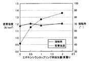
また、トリデカフルオロヘキシルトリメトキシシラン(SIT8176−0)のジイソアミルエーテルに対する濃度を3.0質量%に固定し、エポキシシランカップリング剤である2−(3,4−エポキシシクロヘキシル)エチルトリメトキシシラン(KBM303)の濃度を、0質量%〜2.0質量%でシフトしたときの密着強度と接触角を表3と図14に示す。図14の結果から明らかなとおり、エポキシシランカップリング剤を増量することにより、接触角を70°程度の高い水準に保ちながら、密着強度を13.5N/cm2以上に高めることができた。 In addition, the concentration of tridecafluorohexyltrimethoxysilane (SIT8176-0) with respect to diisoamyl ether was fixed at 3.0% by mass, and 2- (3,4-epoxycyclohexyl) ethyltrimethoxy, which is an epoxysilane coupling agent. Table 3 and FIG. 14 show the adhesion strength and the contact angle when the concentration of silane (KBM303) is shifted from 0% by mass to 2.0% by mass. As is apparent from the results of FIG. 14, by increasing the amount of the epoxysilane coupling agent, the adhesion strength could be increased to 13.5 N / cm 2 or more while maintaining the contact angle at a high level of about 70 °.
(実施例2)
本実施例では、撥水化剤薬液として、撥水化剤薬液Aまたは撥水化剤薬液Bを各々使用した。撥水化剤薬液Aは、実施例1で使用したものを用いた。撥水化剤薬液Bは、有機膜の撥水性向上を主目的として、レジストを溶解しない溶剤を用いて調製した。撥水化剤として、デシルトリメトキシシラン(信越化学(株)製KBM3103C)、KBM7103、または、KBM3103CとKBM7103の混合物(混合比1:1)を使用し、密着強化効果のある撥水化剤としてKBM303を上記の撥水化剤の総質量に対し、混合比3:1に調整し、使用した。各撥水化剤を、ジイソアミルエーテルまたはn-ブチルエーテルに溶解させて、3.0質量%の希釈溶液を調製した。なお、撥水化剤の加水分解を避けるため、使用する溶剤は、蒸留処理、吸収剤の利用または水分除去フィルタの利用により脱水し、水分を50ppm以下とした。
(Example 2)
In this example, the water repellent chemical liquid A or the water repellent chemical liquid B was used as the water repellent chemical liquid, respectively. As the water repellent chemical solution A, the one used in Example 1 was used. The water repellent chemical solution B was prepared using a solvent that does not dissolve the resist, mainly for the purpose of improving the water repellency of the organic film. As a water repellent, decyltrimethoxysilane (KBM3103C manufactured by Shin-Etsu Chemical Co., Ltd.), KBM7103, or a mixture of KBM3103C and KBM7103 (mixing ratio 1: 1) is used as a water repellent with an effect of enhancing adhesion. KBM303 was used by adjusting the mixing ratio to 3: 1 with respect to the total mass of the water repellent agent. Each water repellent was dissolved in diisoamyl ether or n-butyl ether to prepare a 3.0% by weight diluted solution. In order to avoid hydrolysis of the water repellent agent, the solvent used was dehydrated by distillation treatment, use of an absorbent, or use of a water removal filter to make the
本実施例では、図9(a)のプロセスフローに従い、図9(b)と図9(c)に示す構造のウェハを製造した。まず、Si基板1上の被照射面に被加工膜2を形成した後、塗布型有機反射防止膜4を約40nm〜80nmの膜厚で形成し、200℃〜250℃で約1分間〜1.5分間の加熱硬化処理により溶剤を充分に揮発させるとともに、熱反応活性部位の反応でポリマーを架橋させた。その後、メタクリレート系のArF化学増幅型ポジレジスト(膜厚100nm〜200nm)をスピン塗布し、120℃で60秒間ベーク処理を行ない、感光性レジスト層6を形成した。つぎに、図4または図5に示す塗布カップを使用して、図4の場合は、撥水化剤薬液を1000rpmで回転中にストレートノズルで塗布し、図9(c)に示すように、ウェハの天面と、ウェハの側面と、ウェハの底面の周縁部に撥水化処理層3を形成した。また、図5の場合は、撥水化剤薬液を1000rpmで回転中にウェハエッジから0.5mmの位置にノズルを静止させ、ウェハの天面はエッジリンスノズルにより、また底面はバックリンスノズルから撥水化剤薬液を噴射し、塗布した。その結果、パターニングに影響するウェハの天面の中心領域を除き、ウェハの天面の周縁部と、ウェハの側面と、ウェハの底面の周縁部とを撥水化処理することが可能であった。また、撥水化剤薬液のノズルからの噴射時間とウェハの回転数を最適化することにより、撥水化剤の吸着量を制御し、撥水性を調整することができた。
In this example, a wafer having the structure shown in FIGS. 9B and 9C was manufactured according to the process flow of FIG. 9A. First, the
撥水化処理層3を形成した後、液浸露光機で露光処理を施したが、液浸露光時に液浸液のこぼれ落ちは認められなかった。つぎに、テトラメチルアンモニウムハイドロオキサイドの2.38質量%の水溶液で現像処理を行ない、パターン形成を完了し、レジスト膜をマスクにして被加工膜をプラズマドライエッチングした。被加工膜は、トランジスタ形成工程のポリシリコンに関して実施した。いずれの場合もエッチング完了後に、O2プラズマアッシングと、硫酸と過酸化水素水を用いたウェット処理により、レジストと有機反射防止膜を除去した。この際に、先に形成された撥水化処理層は剥離されることも確認された。つづいて、コンタクト工程のシリコン酸化膜を成膜し、その表面を被照射面として、本実施例を繰り返し、コンタクト工程のパターン形成を完了した。同様にメタル工程、ビア工程も繰り返し進めて半導体デバイスを完成した。
After forming the water
(実施例3)
本実施例では、図10(a)のプロセスフローに従い、図10(b)に示す構造のウェハを製造した。撥水化剤薬液は、撥水化剤薬液A単独の場合、撥水化材薬液B単独の場合と、撥水化剤薬液Aと撥水化剤薬液Bの混合品(混合比5:5)の場合について実施した。また、撥水化剤薬液Aは、実施例1で用いたものを使用し、撥水化剤薬液Bは、実施例2で用いたものを使用した。まず、基板1に被加工膜2を形成した後、塗布型有機反射防止膜4を約40nm〜80nmの膜厚で形成し、200℃〜250℃で約1分間〜1.5分間の加熱硬化処理により溶剤を充分に揮発させるとともに熱反応活性部位の反応でポリマーを架橋させた。その後、メタクリレート系のArF化学増幅型ポジレジスト(膜厚100nm〜200nm)をスピン塗布し、120℃で60秒間ベーク処理を行なうことにより感光性レジスト層6を形成した。つぎに、現像液に可溶なトップコート層7を約35nm〜90nmの膜厚で塗布した直後、図5に示す塗布カップを使用して、ウェハの外周部にのみ撥水化処理層3を形成した。撥水化処理層3の形成は、1000rpmの回転中にウェハエッジから0.5mmの位置にノズルを静止させ、ウェハの天面はエッジリンスノズルにより、底面はバックリンスノズルから撥水化剤薬液を噴射し、トップコート層のエッジカットと撥水化反応を同時に進行させて行なった。その後、110℃で60秒間ベーク処理を行ない、レジスト膜を形成した。
(Example 3)
In this example, a wafer having the structure shown in FIG. 10B was manufactured according to the process flow of FIG. The water repellent chemical liquid is the water repellent chemical liquid A alone, the water repellent chemical liquid B alone, or a mixture of the water repellent chemical liquid A and the water repellent chemical liquid B (mixing ratio 5: 5). ). The water repellent chemical solution A used was the one used in Example 1, and the water repellent chemical solution B was the same as that used in Example 2. First, after forming the
撥水化処理層の形成後、基板を液浸露光機で露光した。液浸露光時に、液浸液のこぼれ落ちは認められなかった。つぎに、テトラメチルアンモニウムハイドロオキサイドの2.38質量%水溶液で現像処理を行ない、パターン形成を完了し、このレジスト膜をマスクにして被加工膜をプラズマドライエッチングした。被加工膜は、トランジスタ形成工程のポリシリコンに関して実施した。いずれの場合もエッチング完了後に、O2プラズマアッシングと、硫酸と過酸化水素水を用いたウェット処理によりレジストと有機反射防止膜を除去した。この際に、先に形成された撥水化処理層は剥離されることも確認された。つぎに、コンタクト工程のシリコン酸化膜を成膜し、その表面を被照射面として、本実施例を繰り返し、コンタクト工程のパターン形成を完了した。同様にメタル工程、ビア工程も繰り返し進め半導体デバイスを完成した。 After forming the water repellent treatment layer, the substrate was exposed with an immersion exposure machine. During immersion exposure, no spillage of immersion liquid was observed. Next, development processing was performed with a 2.38 mass% aqueous solution of tetramethylammonium hydroxide to complete pattern formation, and the film to be processed was plasma dry etched using this resist film as a mask. The film to be processed was performed on polysilicon in the transistor formation process. In either case, after the etching was completed, the resist and the organic antireflection film were removed by O 2 plasma ashing and wet treatment using sulfuric acid and hydrogen peroxide. At this time, it was also confirmed that the previously formed water-repellent layer was peeled off. Next, a silicon oxide film in the contact process was formed, and this example was repeated using the surface as an irradiated surface to complete pattern formation in the contact process. Similarly, the metal process and via process were repeated to complete the semiconductor device.
また、トリデカフルオロヘキシルトリメトキシシラン(SIT8176−0)の濃度を3.0質量%に固定し、エポキシシランカップリング剤である2−(3,4−エポキシシクロヘキシル)エチルトリメトキシシラン(KBM303)の濃度を、0質量%〜2.0質量%でシフトした結果、エポキシシランカップリング剤を増量することにより、接触角を高い水準に保ちながら、密着強度を高めることができた。 In addition, the concentration of tridecafluorohexyltrimethoxysilane (SIT8176-0) is fixed to 3.0% by mass, and 2- (3,4-epoxycyclohexyl) ethyltrimethoxysilane (KBM303) which is an epoxysilane coupling agent As a result, the adhesion strength could be increased while maintaining the contact angle at a high level by increasing the amount of the epoxysilane coupling agent.
(実施例4)
本実施例では、撥水化剤薬液として、撥水化剤薬液Dまたは撥水化剤薬液Eを各々使用した。撥水化剤薬液Dは、実施例1で使用したものを用いた。撥水化剤薬液Eは、有機膜の撥水性向上を主目的として、レジストを溶解する溶剤を用いて調製した。撥水化剤としては、デシルトリメトキシシラン(信越化学(株)製KBM3103C)、KBM7103、または、KBM3103CとKBM7103の混合物(混合比1:1)を使用し、密着強化効果のある撥水化剤としてKBM303を上記撥水化剤の総質量に対し混合比3:1に調整し、用意した。各撥水化剤をPGMEAに溶解させて、3.0質量%希釈溶液を調製した。なお、撥水化剤の加水分解を避けるため、使用する溶剤は、蒸留処理、吸収剤の利用または水分除去フィルタの利用により脱水し、水分を50ppm以下とした。
Example 4
In this example, the water repellent chemical liquid D or the water repellent chemical liquid E was used as the water repellent chemical liquid, respectively. As the water repellent chemical solution D, the one used in Example 1 was used. The water repellent chemical solution E was prepared by using a solvent for dissolving a resist mainly for the purpose of improving the water repellency of an organic film. As the water repellent, decyltrimethoxysilane (KBM3103C manufactured by Shin-Etsu Chemical Co., Ltd.), KBM7103, or a mixture of KBM3103C and KBM7103 (mixing ratio 1: 1) is used, and a water repellent having an effect of enhancing adhesion. KBM303 was prepared by adjusting the mixing ratio to 3: 1 with respect to the total mass of the water repellent agent. Each water repellent was dissolved in PGMEA to prepare a 3.0% by weight diluted solution. In order to avoid hydrolysis of the water repellent agent, the solvent used was dehydrated by distillation treatment, use of an absorbent, or use of a water removal filter to make the
本実施例では、図11(a)のプロセスフローに従い、図11(b)に示す構造のウェハを製造した。まず、基板1に被加工膜2を形成した後、塗布型有機反射防止膜4を40nm〜80nmの膜厚で形成し、200℃〜250℃で約1分間〜1.5分間の加熱硬化処理により溶剤を充分に揮発させるとともに熱反応活性部位の反応でポリマーを架橋させた。その後、メタクリレート系のArF化学増幅型ポジレジスト(膜厚100nm〜200nm)をスピン塗布し、感光性レジスト層6を形成した。感光性レジスト層の形成は、図5に示す塗布カップを使用して、撥水化剤薬液を1000rpmの回転中にウェハエッジから0.5mmの位置にノズルを静止させ、ウェハの天面はエッジリンスノズルにより、また底面はバックリンスノズルから撥水化剤薬液を噴射することにより塗布した。また、トップコートのエッジカットと撥水化反応を同時に進行させ、その後、120℃で60秒間ベーク処理を行ない、レジスト膜を形成した。
In this example, a wafer having a structure shown in FIG. 11B was manufactured according to the process flow of FIG. First, after forming the
つぎに、液浸露光機で露光処理を施したが、とくに液浸液のこぼれ落ちは認められなかった。その後、テトラメチルアンモニウムハイドロオキサイドの2.38質量%水溶液で現像処理を行ない、パターン形成を完了した。つぎに、レジスト膜をマスクにして被加工膜をプラズマドライエッチングした。被加工膜は、トランジスタ形成工程のポリシリコンに関して実施した。いずれの場合もエッチング完了後に、O2プラズマアッシングと、硫酸と過酸化水素水を用いたウェット処理によりレジストと有機反射防止膜を除去した。この際に、先に形成された撥水化処理層も剥離されることも確認された。つぎに、コンタクト工程のシリコン酸化膜を成膜し、その表面を被照射面として、本実施例を繰り返し、コンタクト工程のパターン形成を完了した。同様にメタル工程、ビア工程も繰り返し進め半導体デバイスを完成した。 Next, exposure processing was performed with an immersion exposure machine, but no spillage of the immersion liquid was observed. Thereafter, development processing was performed with a 2.38 mass% aqueous solution of tetramethylammonium hydroxide to complete pattern formation. Next, the film to be processed was plasma dry etched using the resist film as a mask. The film to be processed was performed on polysilicon in the transistor formation process. In either case, after the etching was completed, the resist and the organic antireflection film were removed by O 2 plasma ashing and wet treatment using sulfuric acid and hydrogen peroxide. At this time, it was also confirmed that the previously formed water repellent layer was also peeled off. Next, a silicon oxide film in the contact process was formed, and this example was repeated using the surface as an irradiated surface to complete pattern formation in the contact process. Similarly, the metal process and via process were repeated to complete the semiconductor device.
また、トリデカフルオロヘキシルトリメトキシシラン(SIT8176−0)の濃度を3.0質量%に固定し、エポキシシランカップリング剤である2−(3,4−エポキシシクロヘキシル)エチルトリメトキシシラン(KBM303)の濃度を、0質量%〜2.0質量%でシフトした結果、エポキシシランカップリング剤を増量することにより、接触角を高い水準に保ちながら、密着強度を高めることができた。 In addition, the concentration of tridecafluorohexyltrimethoxysilane (SIT8176-0) is fixed to 3.0% by mass, and 2- (3,4-epoxycyclohexyl) ethyltrimethoxysilane (KBM303) which is an epoxysilane coupling agent As a result, the adhesion strength could be increased while maintaining the contact angle at a high level by increasing the amount of the epoxysilane coupling agent.
(実施例5)
本実施例では、図12(a)のプロセスフローに従い、図12(b)に示す構造のウェハを製造した。撥水化剤薬液は、撥水化剤薬液D単独の場合、撥水化剤薬液E単独の場合と、撥水化剤薬液Dと撥水化剤薬液Eの混合品(混合比5:5)の場合について実施した。また、撥水化剤薬液Dは、実施例1で用いたものを使用し、撥水化剤薬液Eは、実施例4で用いたものを使用した。一方、本実施例では、撥水化剤薬液Cまたは撥水化剤薬液Fを使用した。撥水化剤薬液Cは、無機膜と有機膜との密着性の向上を目的とし、レジストを溶解しない溶剤を用いて調製し、3-グリシドキシプロピルメチルトリメトキシシラン(信越化学(株)製KBE403)を、ジイソアミルエーテルまたはn-ブチルエーテルに溶解させて、3.0質量%の希釈溶液としたものを用いた。また、密着向上剤Fは、無機膜と有機膜の密着性の向上を主目的とし、レジストを溶解する溶剤を用いて調製し、3-グリシドキシプロピルメチルトリメトキシシラン(信越化学(株)製KBE403)をPGMEAに溶解させて、3.0質量%の希釈溶液にしたものを用いた。なお、シランカップリング剤を含む撥水化剤薬液の加水分解を避けるため、使用する溶剤は、蒸留処理、吸収剤の利用または水分除去フィルタの利用により脱水し、水分を50ppm以下とした。
(Example 5)
In this example, a wafer having a structure shown in FIG. 12B was manufactured according to the process flow of FIG. The water repellent chemical liquid is the water repellent chemical liquid D alone, the water repellent chemical liquid E alone, or a mixture of the water repellent chemical liquid D and the water repellent chemical liquid E (mixing ratio 5: 5). ). The water repellent chemical solution D used was that used in Example 1, and the water repellent chemical solution E used was that used in Example 4. On the other hand, in this example, the water repellent chemical solution C or the water repellent chemical solution F was used. The water repellent chemical solution C was prepared using a solvent that does not dissolve the resist for the purpose of improving the adhesion between the inorganic film and the organic film, and was prepared using 3-glycidoxypropylmethyltrimethoxysilane (Shin-Etsu Chemical Co., Ltd.). KBE403) manufactured by diisoamyl ether or n-butyl ether was used to prepare a 3.0% by weight diluted solution. Further, the adhesion improver F is mainly prepared to improve the adhesion between the inorganic film and the organic film, and is prepared using a solvent that dissolves the resist, and 3-glycidoxypropylmethyltrimethoxysilane (Shin-Etsu Chemical Co., Ltd.). KBE403) manufactured by dissolving in PGMEA to obtain a 3.0% by mass diluted solution was used. In addition, in order to avoid hydrolysis of the water repellent chemical solution containing the silane coupling agent, the solvent used was dehydrated by distillation treatment, use of an absorbent, or use of a water removal filter, and the water content was adjusted to 50 ppm or less.
まず、基板1に被加工膜2を形成した後、下層有機膜層8を約150nm〜300nmの膜厚で塗布し、200℃〜250℃で約1分間〜1.5分間の加熱硬化処理により溶剤を充分に揮発させるとともに熱反応活性部位の反応でポリマーを架橋形成させた。その後、シリコン含有中間層5として、無機SOG,有機SOGなどのシリセスキオキサン系のポリマー誘導体を約80nm程度の膜厚でスピン塗布し、200℃〜250℃で約1分間〜1.5分間の熱処理により脱水縮合反応、またはエポキシ官能基などの反応活性部位を反応させることにより架橋させた。
First, after forming the
つぎに、図5に示す塗布カップを使用して、1000rpmの回転中にウェハエッジから0.5mmの位置にノズルを静止させ、ウェハの天面はエッジリンスノズルにより、また底面はバックリンスノズルから撥水化剤薬液Cまたは撥水化剤薬液Fを噴射し、密着強化処理層を形成した。常温で反応の完了が困難な場合は、スピナーカップからウェハを搬送し、熱板上、120℃で60秒間加熱した。なお、撥水化剤薬液のノズルからの噴射時間とウェハの回転数を最適化することにより、シランカップリング剤を含む撥水化剤薬液の吸着量を制御し、密着強度を調整することができた。 Next, using the coating cup shown in FIG. 5, the nozzle is stopped at a position 0.5 mm from the wafer edge during rotation at 1000 rpm, the top surface of the wafer is repelled by the edge rinse nozzle, and the bottom surface is repelled from the back rinse nozzle. The hydrating agent chemical solution C or the water repellent agent chemical solution F was sprayed to form an adhesion strengthening treatment layer. When it was difficult to complete the reaction at room temperature, the wafer was transferred from the spinner cup and heated on a hot plate at 120 ° C. for 60 seconds. In addition, by optimizing the spraying time of the water repellent chemical solution from the nozzle and the number of rotations of the wafer, the adsorption amount of the water repellent chemical solution containing the silane coupling agent can be controlled and the adhesion strength can be adjusted. did it.
その後、感光性レジスト層6として、メタクリレート系のArF化学増幅型ポジレジスト(膜厚100nm〜200nm)をスピン塗布した後、図5に示す塗布カップを使用して、1000rpmの回転中にウェハエッジから0.5mmの位置にノズルを静止させ、ウェハの天面はエッジリンスノズルにより、また底面はバックリンスノズルから撥水化剤薬液を噴射し、レジストのエッジカットと撥水化反応を進行させた。その後、120℃で60秒間ベーク処理を行ない、撥水密着強化処理層3aを形成した。
Thereafter, a methacrylate-based ArF chemically amplified positive resist (thickness: 100 nm to 200 nm) is spin-coated as the photosensitive resist
この撥水密着強化処理後の基板を液浸露光機で露光処理を施した結果、液浸液のこぼれ落ちはなく、撥水化剤薬液C単独の場合または撥水化剤薬液F単独の何れの場合においても、液浸液の対流などによるウェハエッジからの剥がれは認められなかった。その後、テトラメチルアンモニウムハイドロオキサイドの2.38質量%の水溶液で現像処理を行ない、パターン形成を完了した。このレジスト膜をマスクにして被加工膜をプラズマドライエッチングした。被加工膜は、トランジスタ形成工程のポリシリコンに関して実施した。いずれの場合もエッチング完了後に、O2プラズマアッシングと、硫酸と過酸化水素水を用いたウェット処理によりレジストと下層有機膜層を除去した。この際、先に形成された撥水密着強化処理層が剥離されることも確認された。 As a result of exposing the substrate after this water repellent adhesion strengthening treatment using an immersion exposure machine, there was no spillage of the immersion liquid, and either the water repellent chemical solution C alone or the water repellent chemical solution F alone was used. Even in this case, peeling from the wafer edge due to convection of the immersion liquid was not recognized. Thereafter, development processing was performed with a 2.38 mass% aqueous solution of tetramethylammonium hydroxide to complete pattern formation. Using this resist film as a mask, the film to be processed was plasma dry etched. The film to be processed was performed on polysilicon in the transistor formation process. In any case, after the etching was completed, the resist and the lower organic film layer were removed by O 2 plasma ashing and wet treatment using sulfuric acid and hydrogen peroxide solution. At this time, it was also confirmed that the previously formed water-repellent adhesion reinforcing treatment layer was peeled off.
本実施例は、トップコート層によりウェハの最表面が覆われていない場合の実施例であり、感光性レジスト層形成後のパターニング工程を図15に示す。まず、図15(a)に示すような、基板1上に、被加工膜2、下層有機膜層8、シリコン含有中間層5と感光性レジスト層6を備えるウェハを露光現像し、図15(b)に示すように、レジストパターン6aを形成した。つぎに、図15(c)に示すように、レジストパターン6aをマスクにして、シリコーン含有中間層5をエッチングした。その後、図15(d)に示すように、中間層パターン5aをマスクにして下層有機膜層8をエッチングし、有機膜層パターン8aを形成した。つづいて、図15(e)に示すように、有機膜層パターン8aをマスクにして被加工膜2をエッチングし、被加工膜パターン2aを形成した。最後に、図15(f)に示すように、有機膜層パターン8aを除去して、パターン形成を完了した。その後、コンタクト工程のシリコン酸化膜を成膜し、その表面を被照射面として、本実施例を繰り返し、コンタクト工程のパターン形成を完了した。同様にメタル工程、ビア工程も繰り返し進め、半導体デバイスを完成した。
In this example, the top surface of the wafer is not covered with the top coat layer, and the patterning process after the formation of the photosensitive resist layer is shown in FIG. First, as shown in FIG. 15A, a wafer provided with a film to be processed 2, a lower
(実施例6)
本実施例では、図13(a)のプロセスフローに従い、図13(b)(c)に示す構造のウェハを製造した。撥水化剤薬液は、つぎのものを各々使用した。
撥水化剤薬液A
撥水化剤薬液G;撥水化剤薬液Aと撥水化剤薬液Cの混合品(混合比5:1)
撥水化剤薬液B
撥水化剤薬液H;撥水化剤薬液Bと撥水化剤薬液Cの混合品(混合比5:1)
撥水化剤薬液I;撥水化剤薬液Aと撥水化剤薬液Bの混合品(混合比5:5)
撥水化剤薬液J;撥水化剤薬液Gと撥水化剤薬液Hの混合品(混合比5:5)
また、撥水化剤薬液Aは実施例1で使用したもの、撥水化剤薬液Bは実施例2で使用したもの、撥水化剤薬液Cは実施例5で使用したものを各々使用した。
(Example 6)
In this example, a wafer having a structure shown in FIGS. 13B and 13C was manufactured according to the process flow of FIG. The following water repellent chemicals were used.
Water repellent chemical A
Water repellent chemical liquid G; mixture of water repellent chemical liquid A and water repellent chemical liquid C (mixing ratio 5: 1)
Water repellent chemical B
Water repellent chemical liquid H; mixture of water repellent chemical liquid B and water repellent chemical liquid C (mixing ratio 5: 1)
Water repellent chemical liquid I; mixture of water repellent chemical liquid A and water repellent chemical liquid B (mixing ratio 5: 5)
Water repellent chemical solution J; mixture of water repellent chemical solution G and water repellent chemical solution H (mixing ratio 5: 5)
Further, the water repellent chemical solution A was used in Example 1, the water repellent chemical solution B was used in Example 2, and the water repellent chemical solution C was used in Example 5. .
まず、基板1上に被加工膜2を形成した後、下層有機膜層8を約150nm〜300nmの膜厚で塗布し、200℃〜250℃で約1分間〜1.5分間の加熱硬化処理により溶剤を充分に揮発させるとともに熱反応活性部位の反応でポリマーを架橋形成させた。その後、シリコン含有中間層5として、無機SOG,有機SOGなどのシリセスキオキサン系のポリマー誘導体を約80nm程度の膜厚でスピン塗布し、200℃〜250℃で約1分間〜1.5分間の熱処理により脱水縮合反応、またはエポキシ官能基などの反応活性部位を反応させることにより架橋させた。
First, after forming the
その後、感光性レジスト層6として、メタクリレート系のArF化学増幅型ポジレジスト(膜厚100nm〜200nm)をスピン塗布し、図4または図5に示す塗布カップを使用して、撥水密着強化処理層3aを形成した。図4の場合は、上記の各撥水化剤薬液を1000rpmの回転中にストレートノズルで塗布し、図13(c)に示すように、撥水密着強化処理層3aを、ウェハの天面と、ウェハの側面と、ウェハの底面の周縁部に形成した。一方、図5の場合は、1000rpmで回転中に、ウェハエッジから0.5mmの位置にノズルを静止させ、ウェハの天面はエッジリンスノズルにより、また底面はバックリンスノズルにより各撥水剤薬液を噴射した。その結果、図13(b)に示すように、撥水密着強化処理層3aは、ウェハの天面の周縁部と、ウェハの側面と、ウェハの底面の周縁部とに形成された。その後、120℃で60秒間ベーク処理を行ない、現像液に可溶なトップコート膜7を約35nm〜90nmの膜厚でレジスト上に塗布し、110℃で60秒間ベーク処理を行なった。
Thereafter, a methacrylate-based ArF chemically amplified positive resist (film thickness: 100 nm to 200 nm) is spin-coated as the photosensitive resist
その後、液浸露光機で露光処理を施した結果、いずれの撥水化剤薬液についても、液浸液のこぼれ落ちはなく、また液浸液の対流などによるウェハエッジからの剥がれは認められなかった。その後、テトラメチルアンモニウムハイドロオキサイドの2.38質量%水溶液で現像処理を行ない、パターン形成を完了し、レジスト膜をマスクにして被加工膜をプラズマドライエッチングした。被加工膜は、トランジスタ形成工程のポリシリコンに関して実施した。いずれの場合もエッチング完了後に、O2プラズマアッシングと、硫酸と過酸化水素水を用いたウェット処理によりレジストと下層有機膜層を除去した。その際、先に形成された撥水密着強化処理層が剥離されることも確認された。 Thereafter, as a result of exposure processing with an immersion exposure machine, no immersion liquid spilled off and no peeling from the wafer edge due to convection of the immersion liquid was observed for any of the water repellent chemicals. Thereafter, development was performed with a 2.38 mass% aqueous solution of tetramethylammonium hydroxide to complete pattern formation, and the film to be processed was plasma dry etched using the resist film as a mask. The film to be processed was performed on polysilicon in the transistor formation process. In any case, after the etching was completed, the resist and the lower organic film layer were removed by O 2 plasma ashing and wet treatment using sulfuric acid and hydrogen peroxide solution. At that time, it was also confirmed that the previously formed water-repellent adhesion reinforcing treatment layer was peeled off.
本実施例のうち、現像液に可溶なトップコート層によりウェハの最表面が覆われ、撥水密着強化処理層をウェハの外周部にのみ形成した態様における、感光性レジスト層形成後のパターニング工程を図16に示す。まず、図16(a)に示すような、基板1上に、被加工膜2、下層有機膜層8、シリコン含有中間層5と感光性レジスト層6を備えるウェハに対して、図16(b)に示すように、現像液に可溶なトップコート層7を形成した。つづいて、図16(c)に示すように露光し、図16(d)に示すように現像し、現像液に可溶なトップコート層7とレジストの露光部6bを除去し、レジストパターン6aを形成した。つぎに、図16(e)に示すように、レジストパターン6aをマスクにして、シリコン含有中間層5をエッチングした。その後、図16(f)に示すように、中間層パターン5aをマスクにして下層有機膜層8をエッチングし、有機膜層パターン8aを形成した。つづいて、図16(g)に示すように、有機膜層パターン8aをマスクにして被加工膜2をエッチングし、被加工膜パターン2aを形成した。最後に、図16(h)に示すように、有機膜層パターン8aを除去して、パターン形成を完了した。その後、コンタクト工程のシリコン酸化膜を成膜し、その表面を被照射面として、本実施例を繰り返し、コンタクト工程のパターン形成を完了した。同様にメタル工程、ビア工程も繰り返し、半導体デバイスを完成した。
In this embodiment, patterning after formation of the photosensitive resist layer in an embodiment in which the outermost surface of the wafer is covered with a developer-soluble topcoat layer and the water-repellent adhesion enhancing treatment layer is formed only on the outer periphery of the wafer. The process is shown in FIG. First, as shown in FIG. 16A, for a wafer provided with a film to be processed 2, a lower
(実施例7)
撥水化剤薬液を変更し、ウェハ全面に撥水化処理を施した以外は、実施例1と同様の手順により、撥水化処理を行ない、その後半導体デバイスを製造した。本実施例では、撥水化剤として、トリデカフルオロヘキシルトリメトキシシラン(GELEST(株)製SIT8176−0)3質量%と、密着強化効果のある撥水化剤として2−(3,4−エポキシシクロヘキシル)エチルトリメトキシシラン(信越化学(株)製KBM303)1質量%とを、イソアミルエーテルに溶解させた薬液3g中に、超純水0.005mlを添加して処理薬液Aを調整した。当該超純水の含有量によって溶剤であるイソアミルエーテルの層分離は起こらなかった。また、対照として超純水を加えない処理薬液Bを調製した。
(Example 7)
A water repellency treatment was performed in the same manner as in Example 1 except that the water repellency chemical was changed and the entire surface of the wafer was subjected to a water repellency treatment, and then a semiconductor device was manufactured. In this example, 3% by mass of tridecafluorohexyltrimethoxysilane (SEL 8176-0 manufactured by GELEST Co., Ltd.) as a water repellent, and 2- (3,4-) as a water repellent having an adhesion enhancing effect. A treatment chemical solution A was prepared by adding 0.005 ml of ultrapure water to 3 g of a chemical solution in which 1% by mass of epoxycyclohexyl) ethyltrimethoxysilane (KBM303 manufactured by Shin-Etsu Chemical Co., Ltd.) was dissolved in isoamyl ether. Layer separation of isoamyl ether as a solvent did not occur depending on the content of the ultrapure water. Moreover, the processing chemical | medical solution B which does not add ultrapure water as a control was prepared.
撥水化処理を施した基板表面の撥水性を評価するため、基板表面における接触角を接触角計(協和界面科学社製)により測定した。処理薬液Bを用いた場合の接触角は、41.4°であり、超純水を添加した処理薬液Aを用いた場合の接触角は54.1°であった。 In order to evaluate the water repellency of the substrate surface subjected to the water repellency treatment, the contact angle on the substrate surface was measured with a contact angle meter (manufactured by Kyowa Interface Science Co., Ltd.). The contact angle when the treatment chemical solution B was used was 41.4 °, and the contact angle when the treatment chemical solution A to which ultrapure water was added was 54.1 °.
(実施例8)
処理薬液Aに添加した超純水の代わりに、アルカリとして2.38%水酸化テトラメチルアンモニウム(TMAH)水溶液を0.001mlと、TMAHの溶解性向上のためにイソプロピルアルコール(IPA)0.04mlを添加した処理薬液Cを用いた以外は、実施例7と同様の手順により、ウェハ全面に撥水化処理を施し、その後半導体デバイスを製造した。なお、対照としては、上記処理薬液Bを用いた。
(Example 8)
Instead of ultrapure water added to treatment chemical A, 0.001 ml of 2.38% tetramethylammonium hydroxide (TMAH) aqueous solution as alkali and 0.04 ml of isopropyl alcohol (IPA) to improve the solubility of TMAH Except for using the treatment chemical solution C to which was added, the entire surface of the wafer was subjected to a water repellency treatment by the same procedure as in Example 7, and then a semiconductor device was manufactured. In addition, the said processing chemical | medical solution B was used as a control.
処理薬液Bを用いた場合の接触角は、41.4°であるが、超純水を添加した処理薬液Aを用いた場合の接触角は58.1°であった。 The contact angle when the treatment chemical solution B was used was 41.4 °, but the contact angle when the treatment chemical solution A to which ultrapure water was added was 58.1 °.
(実施例9)
撥水化剤として、トリデカフルオロヘキシルトリメトキシシラン(GELEST(株)製SIT8176−0)3質量%と、密着強化効果のある撥水化剤として2−(3,4−エポキシシクロヘキシル)エチルトリメトキシシラン(信越化学(株)製KBM303)1質量%とを、イソプロピルアルコール(IPA)に溶解させた薬液3gに、2.38%TMAH水溶液を0.002ml添加した処理薬液D、0.01ml添加した処理薬液E、0.13ml添加した処理薬液Fの3種を調製した。処理薬液Aをこれらの処理薬液D〜Fのそれぞれに変更した以外は、実施例7と同様の手順によりウェハ全面に撥水化処理を施し、その後半導体デバイスを製造した。各処理薬液のpHをpHメータで測定した結果は、処理薬液DはpH7〜8であり、処理薬液EはpH7〜8であり、処理薬液FはpH9〜10であった。
Example 9
As a water repellent, 3% by mass of tridecafluorohexyltrimethoxysilane (SIT8176-0 manufactured by GELEST Co., Ltd.) and 2- (3,4-epoxycyclohexyl) ethyltri as a water repellent with an effect of enhancing adhesion Treatment chemical solution D in which 0.002 ml of 2.38% TMAH aqueous solution is added to 3 g of chemical solution in which 1% by mass of methoxysilane (KBM303 manufactured by Shin-Etsu Chemical Co., Ltd.) is dissolved in isopropyl alcohol (IPA), 0.01 ml is added. Three types of treatment chemical E and 0.13 ml of treatment chemical F added were prepared. Except that the processing chemical solution A was changed to each of these processing chemical solutions D to F, a water repellent treatment was performed on the entire wafer surface by the same procedure as in Example 7, and then a semiconductor device was manufactured. As a result of measuring the pH of each processing chemical solution with a pH meter, the processing chemical solution D was pH 7-8, the processing chemical solution E was pH 7-8, and the processing chemical solution F was pH 9-10.
上記各処理薬液D〜Fを用いた場合の接触角は、105.1°(処理薬液D)、103.7°(処理薬液E)、104.5°(処理薬液F)であり、各薬液間で大差は無かった。また、撥水化処理後のウェハ表面の状態を観測したところ、処理薬液Dの場合は処理ムラがなく、処理薬液Eの場合は、処理ムラが若干観測され、また、処理薬液Fの場合は、処理ムラが観測された。なお、処理ムラの有無は、目視で確認し、処理後のウェハ上に色ムラが見られる場合を処理ムラ有、と判定した。 The contact angles when using each of the treatment chemicals D to F are 105.1 ° (treatment chemical D), 103.7 ° (treatment chemical E), and 104.5 ° (treatment chemical F). There was no big difference between them. Further, when the state of the wafer surface after the water repellent treatment was observed, there was no processing unevenness in the case of the processing chemical solution D, a slight processing unevenness was observed in the case of the processing chemical solution E, and in the case of the processing chemical solution F. Uneven treatment was observed. The presence or absence of processing unevenness was confirmed by visual observation, and it was determined that there was processing unevenness when color unevenness was observed on the processed wafer.
(実施例10)
本実施例では、撥水化処理または密着強化処理の後に、被加工膜の形成や、熱処理がウェハに加えられた場合において、上記処理において高められた撥水性が維持されることを確認するために行なう。
(Example 10)
In this embodiment, in order to confirm that the enhanced water repellency is maintained in the above-described processing when a film to be processed or heat treatment is applied to the wafer after the water repellency treatment or the adhesion strengthening treatment. To do.
撥水化剤として、Rf(フッ素構造物含有)トリメトキシシラン(Rf(フッ素構造物含有)トリメトキシシラン(70409:旭硝子(株)製))1.94質量%と、密着強化効果のある撥水化剤として2−(3,4−エポキシシクロヘキシル)エチルトリメトキシシラン(信越化学(株)製KBM303)0.97質量%とを、アミルアルコールとイソアミルエーテルを体積比3:7で混合した混合溶剤に溶解させて、超純水を1.9質量%となるよう添加した処理薬液Gを調整した。ウェハ上に、ウェハ中央部に処理薬液を滴下するように設定したエッジリンスノズルから、1mlの処理薬液Gを滴下し、実施例7と同様の手順によりウェハ全面の撥水化処理を行なった。このように撥水化処理を行なったウェハを3つ作製し、それぞれ異なる温度で1分間の初期ベーク処理を行なった。その後各ウェハ表面について撥水性を示す接触角を測定した。初期ベーク処理の温度は、それぞれ110℃、130℃、150℃であった。ついで、全てのウェハに対して205℃で1分間のベーク処理を行ない、再度接触角を測定した。初期ベーク温度を110℃とした場合には、接触角は9.7°減少したが、初期ベーク温度が130℃の場合は、減少幅は8.4°であり、150℃の場合は2.6℃の減少にとどまった。また、初期ベーク温度を高く設定した場合は、より低温の処理に比べて減少後のウェハ表面における接触角は増大することがわかった。 As a water repellent, Rf (fluorine structure-containing) trimethoxysilane (Rf (fluorine structure-containing) trimethoxysilane (70409: manufactured by Asahi Glass Co., Ltd.)) 1.94% by mass, and a water-repellent effect having an adhesion strengthening effect 2- (3,4-epoxycyclohexyl) ethyltrimethoxysilane (KBM303 manufactured by Shin-Etsu Chemical Co., Ltd.) 0.97% by mass as a hydrating agent, and amyl alcohol and isoamyl ether mixed at a volume ratio of 3: 7 A treatment chemical solution G was prepared by dissolving in a solvent and adding ultrapure water to 1.9% by mass. On the wafer, 1 ml of the processing chemical solution G was dropped from an edge rinse nozzle set so as to drop the processing chemical solution at the center of the wafer, and water repellent treatment was performed on the entire wafer surface in the same manner as in Example 7. Three wafers subjected to the water repellency treatment as described above were manufactured, and an initial baking treatment was performed for 1 minute at different temperatures. Thereafter, the contact angle showing water repellency was measured for each wafer surface. The temperatures of the initial baking treatment were 110 ° C., 130 ° C., and 150 ° C., respectively. Subsequently, all wafers were baked at 205 ° C. for 1 minute, and the contact angles were measured again. When the initial baking temperature was 110 ° C., the contact angle was decreased by 9.7 °. However, when the initial baking temperature was 130 ° C., the reduction range was 8.4 °, and when the initial baking temperature was 150 ° C., the contact angle decreased by 2. The decrease was only 6 ° C. Further, it was found that when the initial baking temperature is set high, the contact angle on the wafer surface after the decrease is increased as compared with the processing at a lower temperature.
今回開示された実施の形態および実施例はすべての点で例示であって制限的なものではないと考えられるべきである。本発明の範囲は上記した説明ではなくて特許請求の範囲によって示され、特許請求の範囲と均等の意味および範囲内でのすべての変更が含まれることが意図される。 It should be understood that the embodiments and examples disclosed herein are illustrative and non-restrictive in every respect. The scope of the present invention is defined by the terms of the claims, rather than the description above, and is intended to include any modifications within the scope and meaning equivalent to the terms of the claims.
パターン欠陥のない高品質の半導体デバイスを提供することができる。 A high-quality semiconductor device free from pattern defects can be provided.
1 基板、2 被加工膜、3 撥水化処理層、3a 撥水密着強化処理層、4 塗布型有機反射防止膜、5 シリコン含有中間層、6 感光性レジスト層、7 トップコート層、8 下層有機膜層、9 ステージ外周部。
DESCRIPTION OF
Claims (13)
少なくとも撥水化剤と溶剤とからなる撥水化剤薬液で処理した基板を露光するレジストパターンの形成方法。 A method for forming a resist pattern by immersion exposure, in which an objective lens is disposed on a substrate of a semiconductor device on which a film to be processed is formed, and a liquid film is formed between the objective lens and the substrate for exposure.
A resist pattern forming method of exposing a substrate treated with a water repellent chemical solution comprising at least a water repellent agent and a solvent.
前記被加工膜は、前記基板上にスピンコートする工程を含む多層レジスト法により形成され、
少なくとも前記各スピンコートの間、最初のスピンコートの前、および最後のスピンコートの後のいずれかに、前記撥水化剤薬液で処理する工程を含む請求項1〜3のいずれかに記載のレジストパターンの形成方法。 The film to be processed includes a lower organic film layer formed on the substrate, a silicon-containing intermediate layer, and a photosensitive resist layer,
The film to be processed is formed by a multilayer resist method including a step of spin coating on the substrate,
The treatment according to any one of claims 1 to 3, further comprising a step of treating with the water repellent chemical solution at least between each spin coat, before the first spin coat, and after the last spin coat. A method for forming a resist pattern.
前記感光性レジスト層は、前記基板上にスピンコートする工程を含むフォトリソグラフィ工程により形成され、
少なくとも前記各スピンコートの間、最初のスピンコートの前、および最後のスピンコートの後のいずれかに、前記撥水化剤薬液で処理する工程を含む請求項1〜3のいずれかに記載のレジストパターンの形成方法。 The substrate comprises a photosensitive resist layer on the substrate,
The photosensitive resist layer is formed by a photolithography process including a process of spin coating on the substrate,
The process according to any one of claims 1 to 3, further comprising a step of treating with the water repellent chemical solution at least between each of the spin coats, before the first spin coat, and after the last spin coat. A method for forming a resist pattern.
前記トップコート層を形成する前に、前記撥水化剤薬液で処理する工程を含む請求項4または5に記載のレジストパターンの形成方法。 The substrate comprises a topcoat layer,
The method for forming a resist pattern according to claim 4, comprising a step of treating with the water repellent chemical solution before forming the top coat layer.
前記基板の側面、および、前記基板の天面の周縁部、または、前記基板の底面の周縁部、または、基板の天面の周縁部と基板の底面の周縁部とを処理する工程である請求項4〜8のいずれかに記載のレジストパターンの形成方法。 The step of treating with the water repellent chemical is as follows:
A step of processing a side surface of the substrate and a peripheral portion of the top surface of the substrate, a peripheral portion of the bottom surface of the substrate, or a peripheral portion of the top surface of the substrate and a peripheral portion of the bottom surface of the substrate; Item 9. A method for forming a resist pattern according to any one of Items 4 to 8.
前記基板の側面と、前記基板の天面と、前記基板の底面の周縁部とを処理する工程である請求項4〜9のいずれかに記載のレジストパターンの形成方法。 The step of treating with the water repellent chemical is as follows:
The method for forming a resist pattern according to any one of claims 4 to 9, which is a step of processing a side surface of the substrate, a top surface of the substrate, and a peripheral edge portion of a bottom surface of the substrate.
前記基板上に塗布膜を形成する工程と、
前記基板の側面と、前記基板の天面の周縁部と、前記基板の底面の周縁部とにおいて、前記塗布膜を溶解する溶剤により前記塗布膜を除去する工程との後に行ない、
前記塗布膜を溶解除去した領域を、前記撥水化剤薬液により処理する請求項4〜11のいずれかに記載のレジストパターンの形成方法。 The step of treating with the water repellent chemical is as follows:
Forming a coating film on the substrate;
After the step of removing the coating film with a solvent that dissolves the coating film at the side surface of the substrate, the peripheral edge portion of the top surface of the substrate, and the peripheral edge portion of the bottom surface of the substrate,
The method for forming a resist pattern according to any one of claims 4 to 11, wherein a region where the coating film is dissolved and removed is treated with the water repellent chemical solution.
Priority Applications (5)
| Application Number | Priority Date | Filing Date | Title |
|---|---|---|---|
| JP2008021604A JP2008277748A (en) | 2007-03-30 | 2008-01-31 | Method for forming resist pattern, and semiconductor device manufactured by the method |
| TW097110930A TW200845128A (en) | 2007-03-30 | 2008-03-27 | Method of forming resist pattern and semiconductor device manufactured with the same |
| US12/078,098 US20080241489A1 (en) | 2007-03-30 | 2008-03-27 | Method of forming resist pattern and semiconductor device manufactured with the same |
| KR1020080029334A KR20080089296A (en) | 2007-03-30 | 2008-03-28 | Method of forming resist pattern and semiconductor device manufactured with the same |
| EP08005983A EP1975719A3 (en) | 2007-03-30 | 2008-03-28 | Method of forming resist pattern and semiconductor device manufactured with the same |
Applications Claiming Priority (2)
| Application Number | Priority Date | Filing Date | Title |
|---|---|---|---|
| JP2007094042 | 2007-03-30 | ||
| JP2008021604A JP2008277748A (en) | 2007-03-30 | 2008-01-31 | Method for forming resist pattern, and semiconductor device manufactured by the method |
Publications (2)
| Publication Number | Publication Date |
|---|---|
| JP2008277748A true JP2008277748A (en) | 2008-11-13 |
| JP2008277748A5 JP2008277748A5 (en) | 2011-02-03 |
Family
ID=39995700
Family Applications (1)
| Application Number | Title | Priority Date | Filing Date |
|---|---|---|---|
| JP2008021604A Pending JP2008277748A (en) | 2007-03-30 | 2008-01-31 | Method for forming resist pattern, and semiconductor device manufactured by the method |
Country Status (4)
| Country | Link |
|---|---|
| JP (1) | JP2008277748A (en) |
| KR (1) | KR20080089296A (en) |
| CN (1) | CN101276158A (en) |
| TW (1) | TW200845128A (en) |
Cited By (28)
| Publication number | Priority date | Publication date | Assignee | Title |
|---|---|---|---|---|
| JP2009117832A (en) * | 2007-11-06 | 2009-05-28 | Asml Netherlands Bv | Method of preparing substrate for lithography, substrate, device manufacturing method, sealing coating applicator, and sealing coating measuring device |
| JP2010135428A (en) * | 2008-12-02 | 2010-06-17 | Toshiba Corp | Substrate holding member and method of manufacturing semiconductor device |
| WO2010123001A1 (en) * | 2009-04-24 | 2010-10-28 | セントラル硝子株式会社 | Cleaning agent for silicon wafer |
| JP2011009537A (en) * | 2009-06-26 | 2011-01-13 | Tokyo Electron Ltd | Liquid processing apparatus, liquid processing method, and storage medium |
| JP2011129585A (en) * | 2009-12-15 | 2011-06-30 | Toshiba Corp | Apparatus and method of treating surface of semiconductor substrate |
| JP2011233758A (en) * | 2010-04-28 | 2011-11-17 | Tokyo Electron Ltd | Method of processing substrate |
| WO2011145500A1 (en) * | 2010-05-19 | 2011-11-24 | セントラル硝子株式会社 | Chemical for forming protective film |
| WO2011155407A1 (en) * | 2010-06-07 | 2011-12-15 | セントラル硝子株式会社 | Chemical solution for formation of protective film |
| WO2012002145A1 (en) * | 2010-06-30 | 2012-01-05 | セントラル硝子株式会社 | Chemical solution for forming water-repellent protective film |
| WO2012002243A1 (en) * | 2010-06-28 | 2012-01-05 | セントラル硝子株式会社 | Water-repellent protective film formation agent, chemical solution for forming water-repellent protective film, and wafer cleaning method using chemical solution |
| WO2012002200A1 (en) * | 2010-06-30 | 2012-01-05 | セントラル硝子株式会社 | Wafer cleaning method |
| JP2012033881A (en) * | 2010-06-28 | 2012-02-16 | Central Glass Co Ltd | Chemical liquid for forming water-shedding protective film, and method of cleaning wafer using chemical liquid |
| JP2012044065A (en) * | 2010-08-20 | 2012-03-01 | Dainippon Screen Mfg Co Ltd | Method for processing substrate and apparatus for processing substrate |
| KR20120074197A (en) * | 2010-12-27 | 2012-07-05 | 도쿄엘렉트론가부시키가이샤 | Substrate liquid processing apparatus, substrate liquid processing method and computer readable recording medium having substrate liquid processing program |
| JP2012178432A (en) * | 2011-02-25 | 2012-09-13 | Central Glass Co Ltd | Water-repellent protective film forming solution |
| JP2012178431A (en) * | 2011-02-25 | 2012-09-13 | Central Glass Co Ltd | Wafer cleaning method |
| WO2013080832A1 (en) * | 2011-11-29 | 2013-06-06 | セントラル硝子株式会社 | Method for preparing chemical for forming protective membrane |
| WO2013115021A1 (en) * | 2012-02-01 | 2013-08-08 | セントラル硝子株式会社 | Chemical solution for forming water-repellent protective film, chemical solution kit for forming water-repellent protective film, and method for washing wafer |
| KR101396271B1 (en) * | 2010-06-30 | 2014-05-16 | 샌트랄 글래스 컴퍼니 리미티드 | Wafer cleaning method |
| US8821974B2 (en) | 2010-08-20 | 2014-09-02 | Dainippon Screen Mfg. Co., Ltd. | Substrate processing method |
| JP2015079992A (en) * | 2014-12-22 | 2015-04-23 | 株式会社Screenホールディングス | Substrate processing method and substrate processing apparatus |
| US9053924B2 (en) | 2008-12-26 | 2015-06-09 | Central Glass Company, Limited | Cleaning agent for silicon wafer |
| KR101572583B1 (en) * | 2010-06-28 | 2015-11-30 | 샌트랄 글래스 컴퍼니 리미티드 | Water-repellent protective film formation agent, chemical solution for forming water-repellent protective film, and wafer cleaning method using chemical solution |
| US9228120B2 (en) | 2010-06-07 | 2016-01-05 | Central Glass Company, Limited | Liquid chemical for forming protecting film |
| JP2016187037A (en) * | 2011-10-28 | 2016-10-27 | セントラル硝子株式会社 | Method of preparing liquid chemical for forming protective film |
| US9711344B2 (en) | 2015-02-24 | 2017-07-18 | Renesas Electronics Corporation | Semiconductor device manufacturing method using a multilayer resist |
| WO2020105340A1 (en) * | 2018-11-22 | 2020-05-28 | セントラル硝子株式会社 | Beveled part treatment agent composition and method for manufacturing wafer |
| CN113823549A (en) * | 2020-06-19 | 2021-12-21 | 中国科学院微电子研究所 | Method for manufacturing semiconductor structure |
Families Citing this family (12)
| Publication number | Priority date | Publication date | Assignee | Title |
|---|---|---|---|---|
| KR20110018030A (en) * | 2009-08-17 | 2011-02-23 | 주식회사 동진쎄미켐 | A ink composition |
| JP2013118347A (en) * | 2010-12-28 | 2013-06-13 | Central Glass Co Ltd | Cleaning method of wafer |
| JP5611884B2 (en) * | 2011-04-14 | 2014-10-22 | 東京エレクトロン株式会社 | Etching method, etching apparatus and storage medium |
| JP5816488B2 (en) * | 2011-08-26 | 2015-11-18 | ルネサスエレクトロニクス株式会社 | Manufacturing method of semiconductor device |
| CN104145216A (en) * | 2012-04-19 | 2014-11-12 | 木本股份有限公司 | Heat-curable protective liquid for glass mask and glass mask |
| JP5728517B2 (en) * | 2013-04-02 | 2015-06-03 | 富士フイルム株式会社 | Method for producing organic processing liquid for patterning chemically amplified resist film, pattern forming method, and method for producing electronic device |
| CN103293859A (en) * | 2013-05-27 | 2013-09-11 | 苏州扬清芯片科技有限公司 | Method for manufacturing photoresist film |
| SG11201703607RA (en) * | 2014-11-19 | 2017-06-29 | Nissan Chemical Ind Ltd | Composition for forming silicon-containing resist underlayer film removable by wet process |
| JP6730417B2 (en) * | 2017-12-31 | 2020-07-29 | ローム アンド ハース エレクトロニック マテリアルズ エルエルシーRohm and Haas Electronic Materials LLC | Photoresist composition and method |
| WO2019159749A1 (en) * | 2018-02-13 | 2019-08-22 | セントラル硝子株式会社 | Water-repellent protective film-forming agent, water-repellent protective film-forming chemical solution, and wafer surface treatment method |
| JP7297878B2 (en) * | 2018-10-01 | 2023-06-26 | エーエスエムエル ネザーランズ ビー.ブイ. | object in a lithographic apparatus |
| JP7162541B2 (en) * | 2019-01-22 | 2022-10-28 | 東京エレクトロン株式会社 | SUBSTRATE PROCESSING APPARATUS, SUBSTRATE PROCESSING METHOD, AND STORAGE MEDIUM |
Citations (4)
| Publication number | Priority date | Publication date | Assignee | Title |
|---|---|---|---|---|
| JP2005118660A (en) * | 2003-10-16 | 2005-05-12 | Seiko Epson Corp | Liquid repellent region forming method, pattern forming method and electronic device |
| JP2005197469A (en) * | 2004-01-07 | 2005-07-21 | Tokyo Electron Ltd | Coater/developer and coating/developing method |
| JP2007258217A (en) * | 2006-03-20 | 2007-10-04 | Toppan Printing Co Ltd | Printing method |
| JP2008235542A (en) * | 2007-03-20 | 2008-10-02 | Dainippon Printing Co Ltd | Wafer for oil immersion lithography and its manufacturing method |
-
2008
- 2008-01-31 JP JP2008021604A patent/JP2008277748A/en active Pending
- 2008-03-27 TW TW097110930A patent/TW200845128A/en unknown
- 2008-03-28 KR KR1020080029334A patent/KR20080089296A/en not_active Application Discontinuation
- 2008-03-28 CN CNA2008100885739A patent/CN101276158A/en active Pending
Patent Citations (4)
| Publication number | Priority date | Publication date | Assignee | Title |
|---|---|---|---|---|
| JP2005118660A (en) * | 2003-10-16 | 2005-05-12 | Seiko Epson Corp | Liquid repellent region forming method, pattern forming method and electronic device |
| JP2005197469A (en) * | 2004-01-07 | 2005-07-21 | Tokyo Electron Ltd | Coater/developer and coating/developing method |
| JP2007258217A (en) * | 2006-03-20 | 2007-10-04 | Toppan Printing Co Ltd | Printing method |
| JP2008235542A (en) * | 2007-03-20 | 2008-10-02 | Dainippon Printing Co Ltd | Wafer for oil immersion lithography and its manufacturing method |
Cited By (52)
| Publication number | Priority date | Publication date | Assignee | Title |
|---|---|---|---|---|
| US8394572B2 (en) | 2007-11-06 | 2013-03-12 | Asml Netherlands B.V. | Method of preparing a substrate for lithography, a substrate, a device manufacturing method, a sealing coating applicator and a sealing coating measurement apparatus |
| JP2009117832A (en) * | 2007-11-06 | 2009-05-28 | Asml Netherlands Bv | Method of preparing substrate for lithography, substrate, device manufacturing method, sealing coating applicator, and sealing coating measuring device |
| US8114568B2 (en) | 2007-11-06 | 2012-02-14 | Amsl Netherlands B.V. | Method of preparing a substrate for lithography, a substrate, a device manufacturing method, a sealing coating applicator and a sealing coating measurement apparatus |
| JP2010135428A (en) * | 2008-12-02 | 2010-06-17 | Toshiba Corp | Substrate holding member and method of manufacturing semiconductor device |
| US9281178B2 (en) | 2008-12-26 | 2016-03-08 | Central Glass Company, Limited | Cleaning agent for silicon wafer |
| US9053924B2 (en) | 2008-12-26 | 2015-06-09 | Central Glass Company, Limited | Cleaning agent for silicon wafer |
| WO2010123001A1 (en) * | 2009-04-24 | 2010-10-28 | セントラル硝子株式会社 | Cleaning agent for silicon wafer |
| JP2010272852A (en) * | 2009-04-24 | 2010-12-02 | Central Glass Co Ltd | Cleaning agent for silicon wafer |
| JP2011009537A (en) * | 2009-06-26 | 2011-01-13 | Tokyo Electron Ltd | Liquid processing apparatus, liquid processing method, and storage medium |
| KR101421494B1 (en) | 2009-06-26 | 2014-07-22 | 도쿄엘렉트론가부시키가이샤 | Liquid processing apparatus, liquid processing method and storage medium |
| US8617656B2 (en) | 2009-06-26 | 2013-12-31 | Tokyo Electron Limited | Liquid processing apparatus, liquid processing method, and storage medium |
| JP2011129585A (en) * | 2009-12-15 | 2011-06-30 | Toshiba Corp | Apparatus and method of treating surface of semiconductor substrate |
| JP2011233758A (en) * | 2010-04-28 | 2011-11-17 | Tokyo Electron Ltd | Method of processing substrate |
| US9691603B2 (en) | 2010-05-19 | 2017-06-27 | Central Glass Company, Limited | Chemical for forming protective film |
| WO2011145500A1 (en) * | 2010-05-19 | 2011-11-24 | セントラル硝子株式会社 | Chemical for forming protective film |
| KR101483484B1 (en) | 2010-05-19 | 2015-01-16 | 샌트랄 글래스 컴퍼니 리미티드 | Chemical for forming protective film |
| JP2012033873A (en) * | 2010-05-19 | 2012-02-16 | Central Glass Co Ltd | Chemical for formation of protective film |
| KR101363441B1 (en) | 2010-06-07 | 2014-02-21 | 샌트랄 글래스 컴퍼니 리미티드 | Chemical solution for formation of protective film, process for preparing thereof and process for cleaning using the same |
| JPWO2011155407A1 (en) * | 2010-06-07 | 2013-08-01 | セントラル硝子株式会社 | Chemical solution for protective film formation |
| US9748092B2 (en) | 2010-06-07 | 2017-08-29 | Central Glass Company, Limited | Liquid chemical for forming protecting film |
| WO2011155407A1 (en) * | 2010-06-07 | 2011-12-15 | セントラル硝子株式会社 | Chemical solution for formation of protective film |
| JP2016036038A (en) * | 2010-06-07 | 2016-03-17 | セントラル硝子株式会社 | Chemical solution for formation of protective film |
| JP5821844B2 (en) * | 2010-06-07 | 2015-11-24 | セントラル硝子株式会社 | Chemical solution for protective film formation |
| US9228120B2 (en) | 2010-06-07 | 2016-01-05 | Central Glass Company, Limited | Liquid chemical for forming protecting film |
| WO2012002243A1 (en) * | 2010-06-28 | 2012-01-05 | セントラル硝子株式会社 | Water-repellent protective film formation agent, chemical solution for forming water-repellent protective film, and wafer cleaning method using chemical solution |
| KR101572583B1 (en) * | 2010-06-28 | 2015-11-30 | 샌트랄 글래스 컴퍼니 리미티드 | Water-repellent protective film formation agent, chemical solution for forming water-repellent protective film, and wafer cleaning method using chemical solution |
| JP2012033881A (en) * | 2010-06-28 | 2012-02-16 | Central Glass Co Ltd | Chemical liquid for forming water-shedding protective film, and method of cleaning wafer using chemical liquid |
| WO2012002145A1 (en) * | 2010-06-30 | 2012-01-05 | セントラル硝子株式会社 | Chemical solution for forming water-repellent protective film |
| JP2012033880A (en) * | 2010-06-30 | 2012-02-16 | Central Glass Co Ltd | Chemical for forming water repellency protection film |
| KR101396271B1 (en) * | 2010-06-30 | 2014-05-16 | 샌트랄 글래스 컴퍼니 리미티드 | Wafer cleaning method |
| US9090782B2 (en) | 2010-06-30 | 2015-07-28 | Central Glass Company, Limited | Liquid chemical for forming water repellent protective film |
| WO2012002200A1 (en) * | 2010-06-30 | 2012-01-05 | セントラル硝子株式会社 | Wafer cleaning method |
| JP2012044065A (en) * | 2010-08-20 | 2012-03-01 | Dainippon Screen Mfg Co Ltd | Method for processing substrate and apparatus for processing substrate |
| US9005703B2 (en) | 2010-08-20 | 2015-04-14 | SCREEN Holdings Co., Ltd. | Substrate processing method |
| US8821974B2 (en) | 2010-08-20 | 2014-09-02 | Dainippon Screen Mfg. Co., Ltd. | Substrate processing method |
| US9455134B2 (en) | 2010-08-20 | 2016-09-27 | SCREEN Holdings Co., Ltd. | Substrate processing method |
| JP2012138482A (en) * | 2010-12-27 | 2012-07-19 | Tokyo Electron Ltd | Substrate liquid processing apparatus, substrate liquid processing method, and computer readable recording medium in which substrate liquid processing program is recorded |
| KR101583103B1 (en) | 2010-12-27 | 2016-01-07 | 도쿄엘렉트론가부시키가이샤 | Substrate liquid processing apparatus, substrate liquid processing method and computer readable recording medium having substrate liquid processing program |
| KR20120074197A (en) * | 2010-12-27 | 2012-07-05 | 도쿄엘렉트론가부시키가이샤 | Substrate liquid processing apparatus, substrate liquid processing method and computer readable recording medium having substrate liquid processing program |
| JP2012178431A (en) * | 2011-02-25 | 2012-09-13 | Central Glass Co Ltd | Wafer cleaning method |
| JP2012178432A (en) * | 2011-02-25 | 2012-09-13 | Central Glass Co Ltd | Water-repellent protective film forming solution |
| JP2013108044A (en) * | 2011-10-28 | 2013-06-06 | Central Glass Co Ltd | Method for preparing chemical for forming protective film |
| JP2016187037A (en) * | 2011-10-28 | 2016-10-27 | セントラル硝子株式会社 | Method of preparing liquid chemical for forming protective film |
| WO2013080832A1 (en) * | 2011-11-29 | 2013-06-06 | セントラル硝子株式会社 | Method for preparing chemical for forming protective membrane |
| WO2013115021A1 (en) * | 2012-02-01 | 2013-08-08 | セントラル硝子株式会社 | Chemical solution for forming water-repellent protective film, chemical solution kit for forming water-repellent protective film, and method for washing wafer |
| JP2015079992A (en) * | 2014-12-22 | 2015-04-23 | 株式会社Screenホールディングス | Substrate processing method and substrate processing apparatus |
| US9711344B2 (en) | 2015-02-24 | 2017-07-18 | Renesas Electronics Corporation | Semiconductor device manufacturing method using a multilayer resist |
| WO2020105340A1 (en) * | 2018-11-22 | 2020-05-28 | セントラル硝子株式会社 | Beveled part treatment agent composition and method for manufacturing wafer |
| JPWO2020105340A1 (en) * | 2018-11-22 | 2021-10-07 | セントラル硝子株式会社 | Method for manufacturing bevel treatment agent composition and wafer |
| JP7328564B2 (en) | 2018-11-22 | 2023-08-17 | セントラル硝子株式会社 | Bevel treatment agent composition and wafer manufacturing method |
| US11817310B2 (en) | 2018-11-22 | 2023-11-14 | Central Glass Company, Limited | Bevel portion treatment agent composition and method of manufacturing wafer |
| CN113823549A (en) * | 2020-06-19 | 2021-12-21 | 中国科学院微电子研究所 | Method for manufacturing semiconductor structure |
Also Published As
| Publication number | Publication date |
|---|---|
| CN101276158A (en) | 2008-10-01 |
| TW200845128A (en) | 2008-11-16 |
| KR20080089296A (en) | 2008-10-06 |
Similar Documents
| Publication | Publication Date | Title |
|---|---|---|
| JP2008277748A (en) | Method for forming resist pattern, and semiconductor device manufactured by the method | |
| US20080241489A1 (en) | Method of forming resist pattern and semiconductor device manufactured with the same | |
| US8178983B2 (en) | Water repellant composition for substrate to be exposed, method for forming resist pattern, electronic device produced by the formation method, treatment method for imparting water repellency to substrate to be exposed, water repellant set for substrate to be exposed, and treatment method for imparting water repellency to substrate to be exposed using the same | |
| US10474032B2 (en) | Coating compositions | |
| TWI290339B (en) | Liquid immersion exposure method, liquid immersion type exposure device, and manufacturing method of semiconductor | |
| KR102189379B1 (en) | Surface treatment liquid, surface treatment method, hydrophobilization method, and hydrophobilized substrate | |
| US7314691B2 (en) | Mask pattern for semiconductor device fabrication, method of forming the same, method for preparing coating composition for fine pattern formation, and method of fabricating semiconductor device | |
| US20100075504A1 (en) | Method of treating a semiconductor substrate | |
| JP5816488B2 (en) | Manufacturing method of semiconductor device | |
| KR20100015311A (en) | Antireflective coating composition based on a silicon polymer | |
| JP5311331B2 (en) | Development processing method for immersion lithography and electronic device using the development processing method | |
| TW583517B (en) | Surface treatment process for chemically amplified resist and the material thereof | |
| EP3093712A1 (en) | Photolithographic process for manufacturing a semiconductor device | |
| KR20070122250A (en) | Hardmask composition coated under photoresist and process of producing integrated circuit devices using thereof | |
| KR20130101063A (en) | Composition for forming monolayer or multilayer | |
| JP6916731B2 (en) | A method for making a substrate water repellent, a surface treatment agent, and a method for suppressing the collapse of an organic pattern or an inorganic pattern when cleaning the substrate surface with a cleaning liquid. | |
| US20220057715A1 (en) | Substrate treating composition and method for fabricating a semiconductor device using the same | |
| CN101630630B (en) | Method for preventing lateral erosion in wet etching | |
| US7816070B2 (en) | Substrate used for immersion lithography process, method of manufacturing substrate used for immersion lithography process, and immersion lithography |
Legal Events
| Date | Code | Title | Description |
|---|---|---|---|
| A711 | Notification of change in applicant |
Free format text: JAPANESE INTERMEDIATE CODE: A712 Effective date: 20100602 |
|
| A521 | Written amendment |
Free format text: JAPANESE INTERMEDIATE CODE: A523 Effective date: 20101214 |
|
| A621 | Written request for application examination |
Free format text: JAPANESE INTERMEDIATE CODE: A621 Effective date: 20101214 |
|
| A977 | Report on retrieval |
Free format text: JAPANESE INTERMEDIATE CODE: A971007 Effective date: 20121207 |
|
| A131 | Notification of reasons for refusal |
Free format text: JAPANESE INTERMEDIATE CODE: A131 Effective date: 20121218 |
|
| A02 | Decision of refusal |
Free format text: JAPANESE INTERMEDIATE CODE: A02 Effective date: 20130416 |