JP2008269751A - Semiconductor memory device and electronic equipment having semiconductor memory device - Google Patents
Semiconductor memory device and electronic equipment having semiconductor memory device Download PDFInfo
- Publication number
- JP2008269751A JP2008269751A JP2007115087A JP2007115087A JP2008269751A JP 2008269751 A JP2008269751 A JP 2008269751A JP 2007115087 A JP2007115087 A JP 2007115087A JP 2007115087 A JP2007115087 A JP 2007115087A JP 2008269751 A JP2008269751 A JP 2008269751A
- Authority
- JP
- Japan
- Prior art keywords
- transistor
- read
- power supply
- memory cell
- line
- Prior art date
- Legal status (The legal status is an assumption and is not a legal conclusion. Google has not performed a legal analysis and makes no representation as to the accuracy of the status listed.)
- Withdrawn
Links
- 239000004065 semiconductor Substances 0.000 title claims abstract description 228
- 230000015654 memory Effects 0.000 claims abstract description 237
- 238000003860 storage Methods 0.000 claims abstract description 12
- 239000010409 thin film Substances 0.000 claims description 11
- 239000010408 film Substances 0.000 description 275
- 239000000758 substrate Substances 0.000 description 115
- 239000010410 layer Substances 0.000 description 89
- 238000010586 diagram Methods 0.000 description 54
- 238000000034 method Methods 0.000 description 48
- 230000006870 function Effects 0.000 description 35
- XUIMIQQOPSSXEZ-UHFFFAOYSA-N Silicon Chemical compound [Si] XUIMIQQOPSSXEZ-UHFFFAOYSA-N 0.000 description 32
- 239000003990 capacitor Substances 0.000 description 32
- 229910052710 silicon Inorganic materials 0.000 description 32
- 239000010703 silicon Substances 0.000 description 32
- 229910052751 metal Inorganic materials 0.000 description 29
- 239000002184 metal Substances 0.000 description 29
- 239000000463 material Substances 0.000 description 28
- 239000002585 base Substances 0.000 description 25
- 150000002500 ions Chemical class 0.000 description 24
- 239000012535 impurity Substances 0.000 description 22
- PXHVJJICTQNCMI-UHFFFAOYSA-N Nickel Chemical compound [Ni] PXHVJJICTQNCMI-UHFFFAOYSA-N 0.000 description 21
- 230000015572 biosynthetic process Effects 0.000 description 21
- 229910052581 Si3N4 Inorganic materials 0.000 description 20
- HQVNEWCFYHHQES-UHFFFAOYSA-N silicon nitride Chemical compound N12[Si]34N5[Si]62N3[Si]51N64 HQVNEWCFYHHQES-UHFFFAOYSA-N 0.000 description 20
- VYPSYNLAJGMNEJ-UHFFFAOYSA-N silicon dioxide Inorganic materials O=[Si]=O VYPSYNLAJGMNEJ-UHFFFAOYSA-N 0.000 description 19
- 239000010936 titanium Substances 0.000 description 18
- 229910052814 silicon oxide Inorganic materials 0.000 description 17
- 230000005540 biological transmission Effects 0.000 description 14
- 238000005229 chemical vapour deposition Methods 0.000 description 13
- 239000010949 copper Substances 0.000 description 13
- 239000013078 crystal Substances 0.000 description 13
- 238000010438 heat treatment Methods 0.000 description 13
- KDLHZDBZIXYQEI-UHFFFAOYSA-N Palladium Chemical compound [Pd] KDLHZDBZIXYQEI-UHFFFAOYSA-N 0.000 description 12
- 238000004891 communication Methods 0.000 description 12
- 239000011229 interlayer Substances 0.000 description 12
- BASFCYQUMIYNBI-UHFFFAOYSA-N platinum Chemical compound [Pt] BASFCYQUMIYNBI-UHFFFAOYSA-N 0.000 description 12
- 229910052782 aluminium Inorganic materials 0.000 description 11
- XAGFODPZIPBFFR-UHFFFAOYSA-N aluminium Chemical compound [Al] XAGFODPZIPBFFR-UHFFFAOYSA-N 0.000 description 11
- 238000004519 manufacturing process Methods 0.000 description 11
- 239000002356 single layer Substances 0.000 description 11
- 238000004544 sputter deposition Methods 0.000 description 11
- 229910052750 molybdenum Inorganic materials 0.000 description 10
- 239000011733 molybdenum Substances 0.000 description 10
- 239000011347 resin Substances 0.000 description 10
- 229920005989 resin Polymers 0.000 description 10
- ZOKXTWBITQBERF-UHFFFAOYSA-N Molybdenum Chemical compound [Mo] ZOKXTWBITQBERF-UHFFFAOYSA-N 0.000 description 9
- RTAQQCXQSZGOHL-UHFFFAOYSA-N Titanium Chemical compound [Ti] RTAQQCXQSZGOHL-UHFFFAOYSA-N 0.000 description 9
- 238000002425 crystallisation Methods 0.000 description 9
- 239000011521 glass Substances 0.000 description 9
- 239000010931 gold Substances 0.000 description 9
- 230000000717 retained effect Effects 0.000 description 9
- 229910052715 tantalum Inorganic materials 0.000 description 9
- 229910052719 titanium Inorganic materials 0.000 description 9
- RYGMFSIKBFXOCR-UHFFFAOYSA-N Copper Chemical compound [Cu] RYGMFSIKBFXOCR-UHFFFAOYSA-N 0.000 description 8
- 230000008859 change Effects 0.000 description 8
- 229910052802 copper Inorganic materials 0.000 description 8
- 229910052759 nickel Inorganic materials 0.000 description 8
- 238000000206 photolithography Methods 0.000 description 8
- 229910052721 tungsten Inorganic materials 0.000 description 8
- 239000010937 tungsten Substances 0.000 description 8
- 239000000956 alloy Substances 0.000 description 7
- 230000004888 barrier function Effects 0.000 description 7
- 230000008025 crystallization Effects 0.000 description 7
- 238000005530 etching Methods 0.000 description 7
- 239000001301 oxygen Substances 0.000 description 7
- 229910052760 oxygen Inorganic materials 0.000 description 7
- 238000005268 plasma chemical vapour deposition Methods 0.000 description 7
- 238000007650 screen-printing Methods 0.000 description 7
- 229910052709 silver Inorganic materials 0.000 description 7
- 239000004332 silver Substances 0.000 description 7
- GUVRBAGPIYLISA-UHFFFAOYSA-N tantalum atom Chemical compound [Ta] GUVRBAGPIYLISA-UHFFFAOYSA-N 0.000 description 7
- WFKWXMTUELFFGS-UHFFFAOYSA-N tungsten Chemical compound [W] WFKWXMTUELFFGS-UHFFFAOYSA-N 0.000 description 7
- 102100036285 25-hydroxyvitamin D-1 alpha hydroxylase, mitochondrial Human genes 0.000 description 6
- 101000875403 Homo sapiens 25-hydroxyvitamin D-1 alpha hydroxylase, mitochondrial Proteins 0.000 description 6
- BQCADISMDOOEFD-UHFFFAOYSA-N Silver Chemical compound [Ag] BQCADISMDOOEFD-UHFFFAOYSA-N 0.000 description 6
- CSDREXVUYHZDNP-UHFFFAOYSA-N alumanylidynesilicon Chemical compound [Al].[Si] CSDREXVUYHZDNP-UHFFFAOYSA-N 0.000 description 6
- 239000012298 atmosphere Substances 0.000 description 6
- QVGXLLKOCUKJST-UHFFFAOYSA-N atomic oxygen Chemical compound [O] QVGXLLKOCUKJST-UHFFFAOYSA-N 0.000 description 6
- 239000011651 chromium Substances 0.000 description 6
- 150000001875 compounds Chemical class 0.000 description 6
- 239000007789 gas Substances 0.000 description 6
- -1 oxygen radicals Chemical class 0.000 description 6
- 238000009832 plasma treatment Methods 0.000 description 6
- 229910021420 polycrystalline silicon Inorganic materials 0.000 description 6
- 230000008569 process Effects 0.000 description 6
- 230000001681 protective effect Effects 0.000 description 6
- 238000000926 separation method Methods 0.000 description 6
- OAICVXFJPJFONN-UHFFFAOYSA-N Phosphorus Chemical compound [P] OAICVXFJPJFONN-UHFFFAOYSA-N 0.000 description 5
- 238000010894 electron beam technology Methods 0.000 description 5
- PCHJSUWPFVWCPO-UHFFFAOYSA-N gold Chemical compound [Au] PCHJSUWPFVWCPO-UHFFFAOYSA-N 0.000 description 5
- 229910052737 gold Inorganic materials 0.000 description 5
- 239000001257 hydrogen Substances 0.000 description 5
- 229910052739 hydrogen Inorganic materials 0.000 description 5
- 238000005468 ion implantation Methods 0.000 description 5
- 230000001678 irradiating effect Effects 0.000 description 5
- 229910052698 phosphorus Inorganic materials 0.000 description 5
- 239000011574 phosphorus Substances 0.000 description 5
- 238000012545 processing Methods 0.000 description 5
- 229910021332 silicide Inorganic materials 0.000 description 5
- FVBUAEGBCNSCDD-UHFFFAOYSA-N silicide(4-) Chemical compound [Si-4] FVBUAEGBCNSCDD-UHFFFAOYSA-N 0.000 description 5
- OKTJSMMVPCPJKN-UHFFFAOYSA-N Carbon Chemical compound [C] OKTJSMMVPCPJKN-UHFFFAOYSA-N 0.000 description 4
- 230000008901 benefit Effects 0.000 description 4
- UMIVXZPTRXBADB-UHFFFAOYSA-N benzocyclobutene Chemical compound C1=CC=C2CCC2=C1 UMIVXZPTRXBADB-UHFFFAOYSA-N 0.000 description 4
- 229910052799 carbon Inorganic materials 0.000 description 4
- 229910052804 chromium Inorganic materials 0.000 description 4
- 238000005520 cutting process Methods 0.000 description 4
- 229910010272 inorganic material Inorganic materials 0.000 description 4
- 239000011147 inorganic material Substances 0.000 description 4
- 238000002955 isolation Methods 0.000 description 4
- 239000010955 niobium Substances 0.000 description 4
- 239000011368 organic material Substances 0.000 description 4
- 230000010355 oscillation Effects 0.000 description 4
- 229910052763 palladium Inorganic materials 0.000 description 4
- 229910052697 platinum Inorganic materials 0.000 description 4
- 229920005591 polysilicon Polymers 0.000 description 4
- 229910052779 Neodymium Inorganic materials 0.000 description 3
- MWUXSHHQAYIFBG-UHFFFAOYSA-N Nitric oxide Chemical compound O=[N] MWUXSHHQAYIFBG-UHFFFAOYSA-N 0.000 description 3
- 239000004952 Polyamide Substances 0.000 description 3
- 239000004642 Polyimide Substances 0.000 description 3
- NIXOWILDQLNWCW-UHFFFAOYSA-N acrylic acid group Chemical group C(C=C)(=O)O NIXOWILDQLNWCW-UHFFFAOYSA-N 0.000 description 3
- 239000000853 adhesive Substances 0.000 description 3
- 230000001070 adhesive effect Effects 0.000 description 3
- 229910021417 amorphous silicon Inorganic materials 0.000 description 3
- 125000004429 atom Chemical group 0.000 description 3
- 239000000919 ceramic Substances 0.000 description 3
- 238000000151 deposition Methods 0.000 description 3
- 230000008021 deposition Effects 0.000 description 3
- 230000000694 effects Effects 0.000 description 3
- 229910052734 helium Inorganic materials 0.000 description 3
- 238000010884 ion-beam technique Methods 0.000 description 3
- 230000001590 oxidative effect Effects 0.000 description 3
- 239000002245 particle Substances 0.000 description 3
- 238000005498 polishing Methods 0.000 description 3
- 229920002647 polyamide Polymers 0.000 description 3
- 229920001721 polyimide Polymers 0.000 description 3
- 238000007639 printing Methods 0.000 description 3
- 150000003254 radicals Chemical class 0.000 description 3
- 230000003068 static effect Effects 0.000 description 3
- XLYOFNOQVPJJNP-UHFFFAOYSA-N water Substances O XLYOFNOQVPJJNP-UHFFFAOYSA-N 0.000 description 3
- QGZKDVFQNNGYKY-UHFFFAOYSA-N Ammonia Chemical compound N QGZKDVFQNNGYKY-UHFFFAOYSA-N 0.000 description 2
- XKRFYHLGVUSROY-UHFFFAOYSA-N Argon Chemical compound [Ar] XKRFYHLGVUSROY-UHFFFAOYSA-N 0.000 description 2
- IJGRMHOSHXDMSA-UHFFFAOYSA-N Atomic nitrogen Chemical compound N#N IJGRMHOSHXDMSA-UHFFFAOYSA-N 0.000 description 2
- ZOXJGFHDIHLPTG-UHFFFAOYSA-N Boron Chemical compound [B] ZOXJGFHDIHLPTG-UHFFFAOYSA-N 0.000 description 2
- VYZAMTAEIAYCRO-UHFFFAOYSA-N Chromium Chemical compound [Cr] VYZAMTAEIAYCRO-UHFFFAOYSA-N 0.000 description 2
- 239000004593 Epoxy Substances 0.000 description 2
- 229910052691 Erbium Inorganic materials 0.000 description 2
- CBENFWSGALASAD-UHFFFAOYSA-N Ozone Chemical compound [O-][O+]=O CBENFWSGALASAD-UHFFFAOYSA-N 0.000 description 2
- 229910004283 SiO 4 Inorganic materials 0.000 description 2
- 229910052775 Thulium Inorganic materials 0.000 description 2
- NRTOMJZYCJJWKI-UHFFFAOYSA-N Titanium nitride Chemical compound [Ti]#N NRTOMJZYCJJWKI-UHFFFAOYSA-N 0.000 description 2
- 229910052769 Ytterbium Inorganic materials 0.000 description 2
- 238000001994 activation Methods 0.000 description 2
- 229910045601 alloy Inorganic materials 0.000 description 2
- 238000000137 annealing Methods 0.000 description 2
- 229910052786 argon Inorganic materials 0.000 description 2
- 229910052785 arsenic Inorganic materials 0.000 description 2
- RQNWIZPPADIBDY-UHFFFAOYSA-N arsenic atom Chemical compound [As] RQNWIZPPADIBDY-UHFFFAOYSA-N 0.000 description 2
- GPBUGPUPKAGMDK-UHFFFAOYSA-N azanylidynemolybdenum Chemical compound [Mo]#N GPBUGPUPKAGMDK-UHFFFAOYSA-N 0.000 description 2
- 229910052796 boron Inorganic materials 0.000 description 2
- 230000001413 cellular effect Effects 0.000 description 2
- 238000006243 chemical reaction Methods 0.000 description 2
- 229910017052 cobalt Inorganic materials 0.000 description 2
- 239000010941 cobalt Substances 0.000 description 2
- GUTLYIVDDKVIGB-UHFFFAOYSA-N cobalt atom Chemical compound [Co] GUTLYIVDDKVIGB-UHFFFAOYSA-N 0.000 description 2
- 239000004020 conductor Substances 0.000 description 2
- 238000002788 crimping Methods 0.000 description 2
- 229910021419 crystalline silicon Inorganic materials 0.000 description 2
- KPUWHANPEXNPJT-UHFFFAOYSA-N disiloxane Chemical class [SiH3]O[SiH3] KPUWHANPEXNPJT-UHFFFAOYSA-N 0.000 description 2
- 239000002019 doping agent Substances 0.000 description 2
- 238000001312 dry etching Methods 0.000 description 2
- 230000005284 excitation Effects 0.000 description 2
- 230000002349 favourable effect Effects 0.000 description 2
- 229910052839 forsterite Inorganic materials 0.000 description 2
- 238000007646 gravure printing Methods 0.000 description 2
- 229910052736 halogen Inorganic materials 0.000 description 2
- 239000001307 helium Substances 0.000 description 2
- SWQJXJOGLNCZEY-UHFFFAOYSA-N helium atom Chemical compound [He] SWQJXJOGLNCZEY-UHFFFAOYSA-N 0.000 description 2
- 239000012943 hotmelt Substances 0.000 description 2
- 150000002431 hydrogen Chemical class 0.000 description 2
- 239000007943 implant Substances 0.000 description 2
- 239000011261 inert gas Substances 0.000 description 2
- 239000011810 insulating material Substances 0.000 description 2
- 238000003698 laser cutting Methods 0.000 description 2
- 238000004518 low pressure chemical vapour deposition Methods 0.000 description 2
- HCWCAKKEBCNQJP-UHFFFAOYSA-N magnesium orthosilicate Chemical compound [Mg+2].[Mg+2].[O-][Si]([O-])([O-])[O-] HCWCAKKEBCNQJP-UHFFFAOYSA-N 0.000 description 2
- 239000011572 manganese Substances 0.000 description 2
- 229910044991 metal oxide Inorganic materials 0.000 description 2
- 150000004706 metal oxides Chemical class 0.000 description 2
- 229910021421 monocrystalline silicon Inorganic materials 0.000 description 2
- 229910052758 niobium Inorganic materials 0.000 description 2
- GUCVJGMIXFAOAE-UHFFFAOYSA-N niobium atom Chemical compound [Nb] GUCVJGMIXFAOAE-UHFFFAOYSA-N 0.000 description 2
- 150000004767 nitrides Chemical class 0.000 description 2
- 238000005121 nitriding Methods 0.000 description 2
- 238000007254 oxidation reaction Methods 0.000 description 2
- 239000004033 plastic Substances 0.000 description 2
- 238000007747 plating Methods 0.000 description 2
- 239000010453 quartz Substances 0.000 description 2
- 230000009467 reduction Effects 0.000 description 2
- 239000010948 rhodium Substances 0.000 description 2
- 229910000679 solder Inorganic materials 0.000 description 2
- 239000000243 solution Substances 0.000 description 2
- MZLGASXMSKOWSE-UHFFFAOYSA-N tantalum nitride Chemical compound [Ta]#N MZLGASXMSKOWSE-UHFFFAOYSA-N 0.000 description 2
- JBQYATWDVHIOAR-UHFFFAOYSA-N tellanylidenegermanium Chemical compound [Te]=[Ge] JBQYATWDVHIOAR-UHFFFAOYSA-N 0.000 description 2
- JBRZTFJDHDCESZ-UHFFFAOYSA-N AsGa Chemical compound [As]#[Ga] JBRZTFJDHDCESZ-UHFFFAOYSA-N 0.000 description 1
- PXGOKWXKJXAPGV-UHFFFAOYSA-N Fluorine Chemical compound FF PXGOKWXKJXAPGV-UHFFFAOYSA-N 0.000 description 1
- 229910001218 Gallium arsenide Inorganic materials 0.000 description 1
- UFHFLCQGNIYNRP-UHFFFAOYSA-N Hydrogen Chemical compound [H][H] UFHFLCQGNIYNRP-UHFFFAOYSA-N 0.000 description 1
- GPXJNWSHGFTCBW-UHFFFAOYSA-N Indium phosphide Chemical compound [In]#P GPXJNWSHGFTCBW-UHFFFAOYSA-N 0.000 description 1
- XEEYBQQBJWHFJM-UHFFFAOYSA-N Iron Chemical compound [Fe] XEEYBQQBJWHFJM-UHFFFAOYSA-N 0.000 description 1
- PWHULOQIROXLJO-UHFFFAOYSA-N Manganese Chemical compound [Mn] PWHULOQIROXLJO-UHFFFAOYSA-N 0.000 description 1
- KJTLSVCANCCWHF-UHFFFAOYSA-N Ruthenium Chemical compound [Ru] KJTLSVCANCCWHF-UHFFFAOYSA-N 0.000 description 1
- 229910004205 SiNX Inorganic materials 0.000 description 1
- 229910004286 SiNxOy Inorganic materials 0.000 description 1
- BLRPTPMANUNPDV-UHFFFAOYSA-N Silane Chemical compound [SiH4] BLRPTPMANUNPDV-UHFFFAOYSA-N 0.000 description 1
- ATJFFYVFTNAWJD-UHFFFAOYSA-N Tin Chemical compound [Sn] ATJFFYVFTNAWJD-UHFFFAOYSA-N 0.000 description 1
- 238000005411 Van der Waals force Methods 0.000 description 1
- GDFCWFBWQUEQIJ-UHFFFAOYSA-N [B].[P] Chemical compound [B].[P] GDFCWFBWQUEQIJ-UHFFFAOYSA-N 0.000 description 1
- 230000002159 abnormal effect Effects 0.000 description 1
- 230000004913 activation Effects 0.000 description 1
- 239000003513 alkali Substances 0.000 description 1
- 239000005407 aluminoborosilicate glass Substances 0.000 description 1
- 239000005354 aluminosilicate glass Substances 0.000 description 1
- 229910021529 ammonia Inorganic materials 0.000 description 1
- 239000007864 aqueous solution Substances 0.000 description 1
- 229910052788 barium Inorganic materials 0.000 description 1
- DSAJWYNOEDNPEQ-UHFFFAOYSA-N barium atom Chemical compound [Ba] DSAJWYNOEDNPEQ-UHFFFAOYSA-N 0.000 description 1
- YXTPWUNVHCYOSP-UHFFFAOYSA-N bis($l^{2}-silanylidene)molybdenum Chemical compound [Si]=[Mo]=[Si] YXTPWUNVHCYOSP-UHFFFAOYSA-N 0.000 description 1
- 230000000903 blocking effect Effects 0.000 description 1
- 239000005388 borosilicate glass Substances 0.000 description 1
- 239000000969 carrier Substances 0.000 description 1
- 238000003776 cleavage reaction Methods 0.000 description 1
- 238000010168 coupling process Methods 0.000 description 1
- 238000013500 data storage Methods 0.000 description 1
- 230000007547 defect Effects 0.000 description 1
- 238000007872 degassing Methods 0.000 description 1
- 238000006356 dehydrogenation reaction Methods 0.000 description 1
- 230000005684 electric field Effects 0.000 description 1
- 230000005611 electricity Effects 0.000 description 1
- 230000005674 electromagnetic induction Effects 0.000 description 1
- 238000001704 evaporation Methods 0.000 description 1
- 239000000284 extract Substances 0.000 description 1
- 230000005669 field effect Effects 0.000 description 1
- 239000010419 fine particle Substances 0.000 description 1
- 239000011737 fluorine Substances 0.000 description 1
- 229910052731 fluorine Inorganic materials 0.000 description 1
- 229910052732 germanium Inorganic materials 0.000 description 1
- GNPVGFCGXDBREM-UHFFFAOYSA-N germanium atom Chemical compound [Ge] GNPVGFCGXDBREM-UHFFFAOYSA-N 0.000 description 1
- 238000009499 grossing Methods 0.000 description 1
- 150000002367 halogens Chemical class 0.000 description 1
- 238000005984 hydrogenation reaction Methods 0.000 description 1
- 238000002513 implantation Methods 0.000 description 1
- 239000012212 insulator Substances 0.000 description 1
- 229910052741 iridium Inorganic materials 0.000 description 1
- GKOZUEZYRPOHIO-UHFFFAOYSA-N iridium atom Chemical compound [Ir] GKOZUEZYRPOHIO-UHFFFAOYSA-N 0.000 description 1
- 229910052743 krypton Inorganic materials 0.000 description 1
- 238000005224 laser annealing Methods 0.000 description 1
- 238000005499 laser crystallization Methods 0.000 description 1
- 239000007788 liquid Substances 0.000 description 1
- 238000001459 lithography Methods 0.000 description 1
- 229910052748 manganese Inorganic materials 0.000 description 1
- 239000002923 metal particle Substances 0.000 description 1
- 150000002751 molybdenum Chemical class 0.000 description 1
- 229910021344 molybdenum silicide Inorganic materials 0.000 description 1
- 239000002105 nanoparticle Substances 0.000 description 1
- QEFYFXOXNSNQGX-UHFFFAOYSA-N neodymium atom Chemical compound [Nd] QEFYFXOXNSNQGX-UHFFFAOYSA-N 0.000 description 1
- 230000007935 neutral effect Effects 0.000 description 1
- 229910052757 nitrogen Inorganic materials 0.000 description 1
- 239000012299 nitrogen atmosphere Substances 0.000 description 1
- 150000002831 nitrogen free-radicals Chemical class 0.000 description 1
- 150000001282 organosilanes Chemical class 0.000 description 1
- 229910052762 osmium Inorganic materials 0.000 description 1
- SYQBFIAQOQZEGI-UHFFFAOYSA-N osmium atom Chemical compound [Os] SYQBFIAQOQZEGI-UHFFFAOYSA-N 0.000 description 1
- 230000003647 oxidation Effects 0.000 description 1
- 230000003071 parasitic effect Effects 0.000 description 1
- 239000012071 phase Substances 0.000 description 1
- 238000002294 plasma sputter deposition Methods 0.000 description 1
- 238000003825 pressing Methods 0.000 description 1
- 239000011241 protective layer Substances 0.000 description 1
- 230000003252 repetitive effect Effects 0.000 description 1
- 238000012827 research and development Methods 0.000 description 1
- 229910052703 rhodium Inorganic materials 0.000 description 1
- MHOVAHRLVXNVSD-UHFFFAOYSA-N rhodium atom Chemical compound [Rh] MHOVAHRLVXNVSD-UHFFFAOYSA-N 0.000 description 1
- 239000010979 ruby Substances 0.000 description 1
- 229910001750 ruby Inorganic materials 0.000 description 1
- 229910052707 ruthenium Inorganic materials 0.000 description 1
- 229910052594 sapphire Inorganic materials 0.000 description 1
- 239000010980 sapphire Substances 0.000 description 1
- 230000007017 scission Effects 0.000 description 1
- VSZWPYCFIRKVQL-UHFFFAOYSA-N selanylidenegallium;selenium Chemical compound [Se].[Se]=[Ga].[Se]=[Ga] VSZWPYCFIRKVQL-UHFFFAOYSA-N 0.000 description 1
- 230000008054 signal transmission Effects 0.000 description 1
- 229910000077 silane Inorganic materials 0.000 description 1
- 239000007790 solid phase Substances 0.000 description 1
- 238000003746 solid phase reaction Methods 0.000 description 1
- 238000007711 solidification Methods 0.000 description 1
- 230000008023 solidification Effects 0.000 description 1
- 238000000638 solvent extraction Methods 0.000 description 1
- 239000010935 stainless steel Substances 0.000 description 1
- 229910001220 stainless steel Inorganic materials 0.000 description 1
- 239000000126 substance Substances 0.000 description 1
- 238000004381 surface treatment Methods 0.000 description 1
- 238000007725 thermal activation Methods 0.000 description 1
- 229910021341 titanium silicide Inorganic materials 0.000 description 1
- WQJQOUPTWCFRMM-UHFFFAOYSA-N tungsten disilicide Chemical compound [Si]#[W]#[Si] WQJQOUPTWCFRMM-UHFFFAOYSA-N 0.000 description 1
- 229910021342 tungsten silicide Inorganic materials 0.000 description 1
Images


Landscapes
- Static Random-Access Memory (AREA)
- Semiconductor Memories (AREA)
Abstract
Description
本発明は半導体記憶装置に関する。特に不揮発性を有する半導体記憶装置に関する。 The present invention relates to a semiconductor memory device. In particular, the present invention relates to a nonvolatile semiconductor memory device.
半導体特性を利用した記憶装置(以下、半導体記憶装置という)は、複数の電子機器に組み込まれ、多くの製品化がなされている。半導体記憶装置としては、揮発性メモリと不揮発性メモリに大別することができる。揮発性メモリとしては、レジスタ、SRAM(Static Random Access Memory)、DRAM(Dynamic Random Access Memory)が挙げられ、不揮発性メモリとしては、FlashEEPROM(フラッシュメモリ)が挙げられる。 Memory devices using semiconductor characteristics (hereinafter referred to as semiconductor memory devices) are incorporated into a plurality of electronic devices and have been commercialized in many ways. Semiconductor memory devices can be broadly classified into volatile memories and nonvolatile memories. Examples of the volatile memory include a register, an SRAM (Static Random Access Memory), and a DRAM (Dynamic Random Access Memory), and the nonvolatile memory includes a Flash EEPROM (flash memory).
揮発性メモリはデータの読み出しや書き込みの点で、不揮発性メモリより優れた点を有しているものの、電源を切るとデータが消えてしまうといった欠点があった。一方、不揮発性メモリは、電源を切ってもデータが消えないといった利点があるものの、揮発性メモリの読み出しや書き込みの速度に比べて大きく劣る。その為、揮発性メモリであるSRAMの電源を切ってもデータが保持されるSRAMの不揮発化(不揮発性SRAM(Nonvolatile Static Random Access Memory)ともいう)の研究開発が盛んに進められている(特許文献1、特許文献2を参照)。
揮発性メモリを不揮発化するためには、電源が切られた状態で記憶状態を保持できるようにする必要がある。揮発性メモリであるSRAMを構成するメモリセルは、選択トランジスタと、2つのインバーター回路(単にインバータともいう)で構成されるラッチ回路(単にラッチともいう)と、を有している。電源が入力される間にSRAM内のラッチは電源電位(H電位または高電位電源ともいう)またはグラウンド電位(L電位または低電位電源ともいう)を保持している。しかし、電源が切れるとラッチを構成するインバーターの出力がH電位またはL電位の出力を維持できなくなり、その結果揮発性メモリであるSRAM内は記憶状態を保持できない。そのため、SRAM等のラッチを有する揮発性メモリを不揮発性メモリとして用いるには、メモリセル内に強誘電体キャパシタ等の不揮発性のメモリ素子を設ける構成が取られている。強誘電体キャパシタ等の不揮発性のメモリ素子をメモリセル内に有する揮発性メモリは、製造コストが高い、書き込み速度が遅いなどのデメリットがあるといった課題がある。 In order to make the volatile memory non-volatile, it is necessary to be able to maintain the storage state with the power turned off. A memory cell included in an SRAM which is a volatile memory includes a selection transistor and a latch circuit (also simply referred to as a latch) including two inverter circuits (also simply referred to as an inverter). While power is input, the latch in the SRAM holds a power supply potential (also referred to as H potential or high potential power supply) or a ground potential (also referred to as L potential or low potential power supply). However, when the power is turned off, the output of the inverter constituting the latch cannot maintain the output of the H potential or the L potential, and as a result, the storage state cannot be maintained in the SRAM which is a volatile memory. Therefore, in order to use a volatile memory having a latch such as an SRAM as a nonvolatile memory, a configuration in which a nonvolatile memory element such as a ferroelectric capacitor is provided in the memory cell is employed. A volatile memory having a nonvolatile memory element such as a ferroelectric capacitor in a memory cell has disadvantages such as high manufacturing cost and low writing speed.
そこで、本発明は上記問題を鑑み、電源が切れても記憶状態を保持することができ、且つ揮発性メモリと同程度のコストで製造でき、且つ読み出しまたは書き込みの速度が揮発性メモリと同程度の半導体記憶装置を提供することを課題とする。 Therefore, in view of the above problems, the present invention can maintain a memory state even when the power is turned off, can be manufactured at a cost similar to that of a volatile memory, and has a reading or writing speed comparable to that of a volatile memory. It is an object of the present invention to provide a semiconductor memory device.
本発明の一は、メモリセルを選択するためのトランジスタと、メモリセルの記憶状態を保持するためのラッチ回路を有し、ラッチ回路を構成するインバーター回路の高電位電源側にはダイオードが接続され、ラッチ回路に容量素子が接続される構成とする。ラッチ回路を具備する半導体記憶装置において、電源が切られた状態でもラッチ回路に接続された容量素子が電位を保持し、そしてラッチ回路を構成するインバーター回路の高電位電源側に接続されたダイオードが容量素子に保持された電荷のリークを防ぐことができる。その結果、不揮発性を有する半導体記憶装置を安価に提供することができる。 One embodiment of the present invention includes a transistor for selecting a memory cell and a latch circuit for holding the memory state of the memory cell, and a diode is connected to the high potential power supply side of the inverter circuit constituting the latch circuit. The capacitor element is connected to the latch circuit. In a semiconductor memory device having a latch circuit, a capacitor connected to the latch circuit holds a potential even when the power is turned off, and a diode connected to the high potential power supply side of the inverter circuit constituting the latch circuit includes Leakage of charges held in the capacitor can be prevented. As a result, a nonvolatile semiconductor memory device can be provided at low cost.
また本発明の半導体記憶装置の一は、ゲート端子が、リードライトワード線に接続された第1のトランジスタ及び第2のトランジスタと、前記第1のトランジスタに接続されたリードライトビット信号線及び第2のトランジスタに接続されたリードライトビット反転信号線より書き込まれたデータの記憶状態を保持するためのラッチ回路と、を含むメモリセルを有し、前記ラッチ回路を構成する第1のインバーター回路及び第2のインバーター回路は、電源線に接続されたダイオードより電源電位が供給されるように接続されており、前記第1のインバーター回路または前記第2のインバーター回路のいずれかの出力端子には、容量素子が接続されていることを特徴とする。 According to another aspect of the semiconductor memory device of the present invention, the gate terminal has a first transistor and a second transistor connected to the read / write word line, a read / write bit signal line connected to the first transistor, and a second transistor. And a latch circuit for holding a storage state of data written from a read / write bit inversion signal line connected to the two transistors, a first inverter circuit constituting the latch circuit, The second inverter circuit is connected so that a power supply potential is supplied from a diode connected to a power supply line, and the output terminal of either the first inverter circuit or the second inverter circuit has A capacitor element is connected.
また本発明の半導体記憶装置の一は、ゲート端子が、ライトワード線に接続された第1のトランジスタ及び第2のトランジスタと、前記第1のトランジスタに接続されたリードライトビット信号線及び第2のトランジスタに接続されたリードライトビット反転信号線より書き込まれたデータの記憶状態を保持するためのラッチ回路と、ゲート端子が、前記ラッチ回路を構成する第1のインバーター回路または第2のインバーター回路のいずれかの出力端子に接続された第3のトランジスタと、ゲート端子が、リードワード線に接続された第4のトランジスタと、を含むメモリセルを有し、前記第1のインバーター回路及び前記第2のインバーター回路は、電源線に接続されたダイオードより電源電位が供給されるように接続されており、前記第3のトランジスタまたは前記第4のトランジスタのいずれか一方の第1端子は、グラウンド線に接続され、前記第3のトランジスタまたは前記第4のトランジスタのいずれか他方の第1端子は、リードビット線に接続され、前記第3のトランジスタの第2端子と前記第4のトランジスタの第2端子が接続されていることを特徴とする。 According to another aspect of the semiconductor memory device of the present invention, the gate terminal has a first transistor and a second transistor connected to the write word line, a read / write bit signal line connected to the first transistor, and a second transistor. A latch circuit for holding a storage state of data written from a read / write bit inversion signal line connected to the transistor of the first and second gates, wherein the gate terminal constitutes the latch circuit A memory cell including a third transistor connected to any one of the output terminals and a fourth transistor having a gate terminal connected to a read word line, and the first inverter circuit and the first transistor The inverter circuit 2 is connected so that a power supply potential is supplied from a diode connected to the power supply line. The first terminal of either the third transistor or the fourth transistor is connected to the ground line, and the other first terminal of the third transistor or the fourth transistor is connected to the read bit line. The second terminal of the third transistor is connected to the second terminal of the fourth transistor.
また本発明の半導体記憶装置の一は、ゲート端子が、ライトワード線に接続された第1のトランジスタ及び第2のトランジスタと、前記第1のトランジスタに接続されたリードライトビット信号線及び第2のトランジスタに接続されたリードライトビット反転信号線より書き込まれたデータの記憶状態を保持するためのラッチ回路と、ゲート端子が、前記ラッチ回路を構成する第1のインバーター回路の出力端子に接続された第3のトランジスタと、ゲート端子が、前記ラッチ回路を構成する第2のインバーター回路の出力端子に接続された第5のトランジスタと、ゲート端子が、第1のリードワード線に接続された第4のトランジスタと、ゲート端子が、第2のリードワード線に接続された第6のトランジスタと、を含むメモリセルを有し、前記第1のインバーター回路及び前記第2のインバーター回路は、電源線に接続されたダイオードより電源電位が供給されるように接続されており、前記第3のトランジスタまたは前記第4のトランジスタのいずれか一方の第1端子は、グラウンド線に接続され、前記第3のトランジスタまたは前記第4のトランジスタのいずれか他方の第1端子は、第1のリードビット線に接続され、前記第3のトランジスタの第2端子と前記第4のトランジスタの第2端子が接続されており、前記第5のトランジスタまたは前記第6のトランジスタのいずれか一方の第1端子は、前記グラウンド線に接続され、前記第5のトランジスタまたは前記第6のトランジスタのいずれか他方の第1端子は、第2のリードビット線に接続され、前記第5のトランジスタの第2端子と前記第5のトランジスタの第2端子が接続されていることを特徴とする。 According to another aspect of the semiconductor memory device of the present invention, the gate terminal has a first transistor and a second transistor connected to the write word line, a read / write bit signal line connected to the first transistor, and a second transistor. The latch circuit for holding the storage state of the data written from the read / write bit inversion signal line connected to the transistor and the gate terminal are connected to the output terminal of the first inverter circuit constituting the latch circuit. The third transistor, the fifth transistor whose gate terminal is connected to the output terminal of the second inverter circuit constituting the latch circuit, and the first transistor whose gate terminal is connected to the first read word line. 4 and a sixth transistor having a gate terminal connected to the second read word line. The first inverter circuit and the second inverter circuit are connected so that a power supply potential is supplied from a diode connected to a power supply line, and either the third transistor or the fourth transistor is connected. One first terminal is connected to a ground line, and the other first terminal of the third transistor or the fourth transistor is connected to a first read bit line, and A second terminal and a second terminal of the fourth transistor are connected, and a first terminal of one of the fifth transistor and the sixth transistor is connected to the ground line, and the fifth terminal The other first terminal of the sixth transistor or the sixth transistor is connected to the second read bit line, and the fifth transistor Wherein the second terminal of the second terminal fifth transistor of motor is connected.
本発明により、書き込み速度が向上し、且つ製造コストが安価な、不揮発性を有する半導体記憶装置を提供することができる。また本発明の半導体記憶装置は、不揮発性を有するため、データの書き込みまたはデータの読み出しを行わない状態のときに、電源を切った状態で記憶状態を保持することができ、低消費電力化を図ることができる。 According to the present invention, a nonvolatile semiconductor memory device with improved writing speed and low manufacturing cost can be provided. In addition, since the semiconductor memory device of the present invention is non-volatile, the memory state can be maintained with the power turned off when data is not written or read, and power consumption is reduced. Can be planned.
以下に、本発明の実施の形態を図面に基づいて説明する。但し、本発明は多くの異なる態様で実施することが可能であり、本発明の趣旨及びその範囲から逸脱することなくその形態及び詳細を様々に変更し得ることは当業者であれば容易に理解される。従って、本実施の形態の記載内容に限定して解釈されるものではない。なお、実施の形態を説明するための全図において、同一部分又は同様な機能を有する部分には同一の符号を付し、その繰り返しの説明は省略する。
(実施の形態1)
Embodiments of the present invention will be described below with reference to the drawings. However, the present invention can be implemented in many different modes, and those skilled in the art can easily understand that the modes and details can be variously changed without departing from the spirit and scope of the present invention. Is done. Therefore, the present invention is not construed as being limited to the description of this embodiment mode. Note that in all the drawings for describing the embodiments, the same portions or portions having similar functions are denoted by the same reference numerals, and repetitive description thereof is omitted.
(Embodiment 1)
本実施の形態では、不揮発性を有する半導体記憶装置の構成について、ブロック図及び回路図等を用いて説明する。なお、本明細書における半導体記憶装置とは、半導体特性を利用してデータの記憶状態を保持する記憶装置のことをいう。 In this embodiment, a structure of a nonvolatile semiconductor memory device is described with reference to a block diagram, a circuit diagram, and the like. Note that a semiconductor memory device in this specification refers to a memory device that retains a data storage state using semiconductor characteristics.
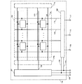
図1に本実施の形態で説明する不揮発性を有する半導体記憶装置のブロック図を示す。図1に示す半導体記憶装置100は、デコーダ101と、書き込み読み出し回路102と、メモリセルアレイ103と、から構成される。デコーダ101は、第1のアドレス信号線104と、ライトイネーブル信号線105と、リードイネーブル信号線106が接続される。またデコーダ101は、複数のメモリセル107と、リードライトワード線108を介して、接続される。書き込み読み出し回路102は、ライトイネーブル信号線105と、リードイネーブル信号線106と、第2のアドレス信号線109と、入力データ信号線110と、出力データ信号線111が接続される。また書き込み読み出し回路102は、複数のメモリセル107と、リードライトビット信号線112と、リードライトビット反転信号線113とに接続される。また半導体記憶装置100には、複数のメモリセルに、電源電位(H電位または高電位電源ともいう。また図中で”1”と表記)する。)及びグラウンド電位(L電位または低電位電源ともいう。また図中”0”と表記する。)を供給するための第1の電源制御回路114a、第2の電源制御回路114bを有している。第1の電源制御回路114a及び第2の電源制御回路114bと、複数のメモリセル107は、メモリセル107に電源電位を入力するための電源線115と、グラウンド電位を入力するためのグラウンド線116を介して、接続される。
FIG. 1 is a block diagram of a nonvolatile semiconductor memory device described in this embodiment. A
なお、本実施の形態において、リードライトワード線とは、メモリセルのデータの読み出し及び書き込みを行うためのワード線のことをいう。また、リードライトビット線及びリードライトビット反転信号線とは、メモリセルのデータの読み出し及び書き込みを行うためのビット線及びビット反転信号線のことをいう。 Note that in this embodiment mode, a read / write word line refers to a word line for reading and writing data in a memory cell. The read / write bit line and the read / write bit inversion signal line refer to a bit line and a bit inversion signal line for reading and writing data in the memory cell.
なお本明細書では、ビット線の本数をビット数、ワード線の本数をライン数ともいう。 In this specification, the number of bit lines is also referred to as the number of bits, and the number of word lines is also referred to as the number of lines.
なお、本実施の形態では、半導体記憶装置100に、第1の電源制御回路114a、第2の電源制御回路114bを2つ配置する構成としたが、いずれか一方であればよい。図1に示すように、メモリセルアレイ103の両側より、電源電位及びグラウンド電位を供給する構成とすることによって、より確実に複数のメモリセルに、所望の電位を供給することができる。
In this embodiment, the first power
図1において、メモリセル107は、1ビットの値を保持することができる。そして、メモリセルアレイ103はメモリセル107を(ビット数)×(ライン数)の個数分、有する。
In FIG. 1, the
書き込み読み出し回路102は半導体記憶装置100の外部から入力データ信号線110から入力されるデータをメモリセルアレイ103の各メモリセル107に書き込む処理と、メモリセルアレイ103の各メモリセル107からデータを読み出して出力データ信号線111によってメモリの外部にデータを送信する処理を行う。
The write /
デコーダ101は半導体記憶装置100の外部から、第1のアドレス信号線より入力されるアドレスに応じて、リードライトワード線108に信号を出力する。
The
デコーダ101はリードライトワード線108へ信号を出力し、各メモリセル107でのデータの読み出しと書き込みを制御する。例えば、書き込み時には、リードライトワード線108の一つが高電位の状態(以下、「H電位」と記す。また図中”1”と表記する。)となり、読み出し時には、リードライトワード線108の一つがH電位となる。なお、リードライトワード線108が選択されない状態ではグラウンド電位の状態(以下、「L電位」と記す。また図中”0”と表記する。)となる。
The
リードライトビット信号線112及びリードライトビット反転信号線113は、それぞれ読み出し用及び書き込み用のビット線である。読み出し時にはアドレスによって選択されたメモリセルの値がリードライトビット信号線112及びリードライトビット反転信号線113に入力され、書き込み時には外部からのデータがリードライトビット信号線112及びリードライトビット反転信号線113に入力される。
The read / write
このような半導体記憶装置100によって、ビット数及びライン数に応じた情報を記憶することができる。
With such a
次に図2(a)で、図1のメモリセル107の回路図について説明する。図2(a)に示すメモリセル107は、図1でも示したように、リードライトワード線108、リードライトビット信号線112、リードライトビット反転信号線113、電源線115、及びグラウンド線116に接続される。メモリセル107は、第1のNチャネル型トランジスタ201a(第1のトランジスタともいう)、第2のNチャネル型トランジスタ201b(第2のトランジスタともいう)、ラッチ回路202、ダイオード203、第1の容量素子204a、及び第2の容量素子204bを有する。
Next, a circuit diagram of the
図2(a)において、第1のNチャネル型トランジスタ201aは、リードライトワード線108の電位に基づいて、リードライトビット信号線112の電位をラッチ回路202に入力するかを切り替えるスイッチとしての機能を有する。また第2のNチャネル型トランジスタ201bは、リードライトワード線108の電位に基づいて、リードライトビット反転信号線113の電位をラッチ回路202に入力するかを切り替えるスイッチとしての機能を有する。また、ダイオード203は、電源線115からの電源電位をラッチ回路202に供給し、且つラッチ回路から電荷のリークのないようにする機能を有する。また第1の容量素子204aは、ラッチ回路の一方のノード(一方のインバーター回路の出力端子)とグラウンド線116に接続され、ラッチ回路202の一方のノードの電位を保持する機能を有する。また第2の容量素子204bは、ラッチ回路の他方のノード(他方のインバーター回路の出力端子)とグラウンド線116に接続され、ラッチ回路202の他方のノードの電位を保持する機能を有する。
In FIG. 2A, the first N-
図2(b)は、図2(a)の動作を説明するために、図2(a)と等価の回路図について示している。ラッチ回路202は、第1のインバーター回路202a、第2のインバーター回路202bを有し、互いに入力端子と出力端子がそれぞれ接続される。第1のインバーター回路202aは、Nチャネル型トランジスタ251及びPチャネル型トランジスタ252を有する。Pチャネル型トランジスタ252の第1端子にはダイオードが電源線115から電源電位を供給するように接続されている。Pチャネル型トランジスタ252の第2端子は、Nチャネル型トランジスタ251の第1端子に接続されている。Nチャネル型トランジスタ251の第2端子は、グラウンド線116に接続される。また、Pチャネル型トランジスタ254の第1端子にはダイオードが電源線115から電源電位を供給するように接続されている。Pチャネル型トランジスタ254の第2端子は、Nチャネル型トランジスタ253の第1端子に接続されている。Nチャネル型トランジスタ253の第2端子は、グラウンド線116に接続される。
FIG. 2B shows a circuit diagram equivalent to FIG. 2A in order to explain the operation of FIG. The
なお、トランジスタとは、ゲートと、ドレインと、ソースとを含む少なくとも三つの端子を有する素子であり、ドレイン領域とソース領域の間にチャネル領域を有しており、ドレイン領域とチャネル領域とソース領域とを介して電流を流すことができるものである。ここで、ソースとドレインとは、トランジスタの構造や動作条件等によって変わるため、いずれがソースまたはドレインであるかを限定することが困難である。そこで、本書類(明細書、特許請求の範囲又は図面など)においては、ソース及びドレインとして機能する領域を、ソースもしくはドレインと呼ばない場合がある。その場合、一例としては、それぞれを第1端子、第2端子と表記する。またゲートについては、ゲート端子と表記する。なお、本書類(明細書、特許請求の範囲又は図面など)においては、メモリセルを構成するトランジスタについて、説明のため、Nチャネル型のトランジスタまたはPチャネル型のトランジスタを使い分けて説明する。しかし、トランジスタを単にスイッチとして用いる際には、Nチャネル型のトランジスタまたはPチャネル型のトランジスタのいずれでもよい。この場合、単にトランジスタと表記する場合もある。 Note that a transistor is an element having at least three terminals including a gate, a drain, and a source. The transistor has a channel region between the drain region and the source region, and the drain region, the channel region, and the source region. A current can be passed through the. Here, since the source and the drain vary depending on the structure and operating conditions of the transistor, it is difficult to limit which is the source or the drain. Therefore, in this document (the specification, the claims, the drawings, and the like), a region functioning as a source and a drain may not be referred to as a source or a drain. In that case, as an example, they are referred to as a first terminal and a second terminal, respectively. The gate is expressed as a gate terminal. Note that in this document (the specification, the claims, the drawings, and the like), an N-channel transistor or a P-channel transistor will be described separately for the transistors included in the memory cell for description. However, when a transistor is simply used as a switch, either an N-channel transistor or a P-channel transistor may be used. In this case, it may be simply expressed as a transistor.
なお本実施の形態において、図1のメモリセル107にデータ「1」が書き込まれているとは、第1のインバーター回路202aの入力端子であるノード281の電位がH電位、かつ第2のインバーター回路202bの入力端子であるノード282の電位がL電位であることをいう。また、データ「0」が書き込まれているとは、第1のインバーター回路202aの入力端子であるノード281の電位がL電位、かつ第2のインバーター回路202bの入力端子であるノード282の電位がH電位であることをいう。
Note that in this embodiment, data “1” is written in the
図3(a)、図3(b)は、図2(b)に示したメモリセルの回路図において、データ「1」を保持している場合に、電源が切られた際の各配線及びノードの状態、並びに各トランジスタのオン又はオフの状態について示し、動作を説明する図である。 3A and 3B are circuit diagrams of the memory cell shown in FIG. 2B. In the case where data “1” is held, each wiring when the power is turned off and It is a figure which shows the state of a node and the on or off state of each transistor, and demonstrates operation | movement.
まず図3(a)で、データ「1」を保持したメモリセルに接続された各配線及びノードの電位の状態、並びに各トランジスタのオン又はオフについて説明する。図3(a)で、ノード281にデータ「1」が入力またはノード282にデータ「0」が入力されると、インバーター回路を構成するトランジスタのオンまたはオフが決まることにより、電源線115の電源電位(図中”1”と表記)またはグラウンド線116のグラウンド電位(図中”0”と表記)より、インバーター回路の出力端子の電位が決定される。
First, referring to FIG. 3A, the state of the potential of each wiring and node connected to the memory cell holding data “1” and the on / off state of each transistor will be described. In FIG. 3A, when data “1” is input to the
図3(a)のようにして、メモリセルは電源線115からの電源電位が供給されている間、データ「1」を保持する。
As shown in FIG. 3A, the memory cell holds data “1” while the power supply potential from the
次に図3(b)で電源が切られた状態、すなわち電源線115の電源電位がグラウンド電位になった際の、データ「1」を保持したメモリセルに接続された各配線及びノードの電位の状態、並びに各トランジスタのオン又はオフについて説明する。図3(b)で、ノード281のデータ「1」は、電源線115の電源電位がグラウンド電位になることによって、第1のインバーター回路202aの出力端子の電位が第1のインバーター回路202aを構成するトランジスタのオン又はオフが変化しないため、ノード282のデータは「0」のままである。一方、図3(b)で、ノード282のデータ「0」は、第1のインバーター回路202aを構成するトランジスタのオン又はオフが変化しないものの、電源線115の電源電位がグラウンド電位になることによって、第2のインバーター回路202bの出力端子に電源線からの電源電位が供給されなくなる。
Next, when the power is turned off in FIG. 3B, that is, when the power supply potential of the
図3(b)で説明したように、電源線115より電源電位が供給されなくなる場合に、ノード281の電位が保持されることを図5(a)を用いて説明する。図5(a)に示すように、ノード281の電位は、第1の容量素子204aに保持され、且つ第1のインバーター回路202aを構成するトランジスタのゲート端子及び第2のインバーター回路202bのPチャネルトランジスタに接続されたダイオード203によって電荷のリークを防ぐことができる。そのため電源が切られた状態でもデータの保持ができるため、不揮発性を有する半導体記憶装置が得られる。
As described with reference to FIG. 3B, the case where the potential of the
また、図4(a)で、データ「0」を保持したメモリセルに接続された各配線及びノードの電位の状態、並びに各トランジスタのオン又はオフについて説明する。図4(a)で、ノード281にデータ「0」が入力またはノード282にデータ「1」が入力されると、インバーター回路を構成するトランジスタのオンまたはオフが決まることにより、電源線115の電源電位またはグラウンド線116のグラウンド電位より、インバーター回路の出力端子の電位が決定される。
In addition, with reference to FIG. 4A, the state of the potential of each wiring and node connected to the memory cell holding data “0” and the on / off state of each transistor will be described. In FIG. 4A, when data “0” is input to the
図4(a)のようにして、メモリセルは電源線115からの電源電位が供給されている間、データ「0」を保持する。
As shown in FIG. 4A, the memory cell holds data “0” while the power supply potential from the
次に図4(b)で電源が切られた状態、すなわち電源線115の電源電位がグラウンド電位になった際の、データ「0」を保持したメモリセルに接続された各配線及びノードの電位の状態、並びに各トランジスタのオン又はオフについて説明する。図4(b)で、ノード282のデータ「1」は、電源線115の電源電位がグラウンド電位になることによって、第2のインバーター回路202bの出力端子の電位が第2のインバーター回路202bを構成するトランジスタのオン又はオフが変化しないため、ノード281のデータは「0」のままである。一方、図4(b)で、ノード281のデータ「0」は、第1のインバーター回路202aを構成するトランジスタのオン又はオフが変化しないものの、電源線115の電源電位がグラウンド電位になることによって、第1のインバーター回路202aの出力端子に電源線からの電源電位が供給されなくなる。
Next, when the power is turned off in FIG. 4B, that is, when the power supply potential of the
図4(b)で説明したように、電源線115より電源電位が供給されなくなる場合に、ノード282の電位が保持されることを図5(b)を用いて説明する。図5(b)に示すように、ノード282の電位は、第2の容量素子204bに保持され、且つ第2のインバーター回路202bを構成するトランジスタのゲート端子及び第1のインバーター回路202aのPチャネルトランジスタに接続されたダイオード203によって電荷のリークを防ぐことができる。そのため電源が切られた状態でもデータの保持ができるため、不揮発性を有する半導体記憶装置が得られる。
As described with reference to FIG. 4B, the fact that the potential of the
なお本実施の形態では、ダイオード203をメモリセル毎に設ける構成について示したが、これに限定されない。ダイオードは、電源線毎に設ける構成であってもよい。電源線毎にダイオードを設ける構成とすることにより、メモリセルの小型化を図りつつ、且つ各メモリセルの不揮発性化を図ることができる。
Note that although a structure in which the
本実施の形態で説明した半導体記憶装置のメモリセルが有するダイオード及び容量素子によって、上述したように電源が切られた状態でもデータの保持ができる。メモリセルはデータ「1」またはデータ「0」のいずれかを保持すれば、再度電源線より電源電位が供給された場合に、第1の容量素子204a、第2の容量素子204bのいずれかに保持された電荷に基づいて、メモリセルはデータを再度保持し続けることができる。そのため、容量素子は第1の容量素子204a及び第2の容量素子204bの両方を具備する構成に限らずに、図6(a)に示すように、図2(a)に示したメモリセルにおいて、第1の容量素子204aのみを配し、データの保持を行っても良い。また図6(b)に示すように、図2(a)に示したメモリセルにおいて、第2の容量素子204bのみを配し、データの保持を行ってもよい。メモリセルの設けられる容量素子を、ラッチ回路の一方のノードにのみ接続する構成とすることによって、メモリセルの小型化に寄与することができる。
With the diode and the capacitor included in the memory cell of the semiconductor memory device described in this embodiment, data can be held even when the power is turned off as described above. If the memory cell holds either data “1” or data “0”, when the power supply potential is supplied again from the power supply line, either the
また、本実施形態で説明した半導体記憶装置のメモリセルでは、ラッチ回路に供給する電源線からの電源電位を常時供給することなく、データの保持をおこなうことが可能となる。そのため、本実施形態で説明した半導体記憶装置のメモリセルでは、データの保持を行う上で、一定期間毎に電源電位の供給を行う構成とすればよいため、消費電力を低減することができる。 In the memory cell of the semiconductor memory device described in this embodiment, data can be retained without always supplying the power supply potential from the power supply line supplied to the latch circuit. Therefore, in the memory cell of the semiconductor memory device described in this embodiment, power supply can be reduced because data power can be supplied every certain period in order to hold data.
なお、本実施の形態は、本明細書の実施の形態の技術的要素と組み合わせて行うことができる。
(実施の形態2)
Note that this embodiment mode can be implemented in combination with the technical elements of the embodiment modes in this specification.
(Embodiment 2)
本実施の形態では、不揮発性を有する半導体記憶装置の構成で、上記実施の形態とは異なる構成について、ブロック図及び回路図等を用いて説明する。本実施の形態で説明する半導体記憶装置では、上記実施の形態1で述べた効果に加えて、メモリセルからのデータの読み出しと書き込みを別の配線を用いて行うことにより、データの読み出しと書き込みをより確実に、且つ高速に行うことのできる半導体記憶装置の構成について詳述する。
In this embodiment, a structure of a nonvolatile semiconductor memory device which is different from the above embodiment will be described with reference to a block diagram, a circuit diagram, and the like. In the semiconductor memory device described in this embodiment, in addition to the effects described in
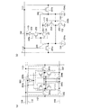
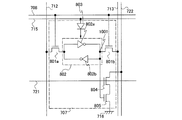
図7に本実施の形態で説明する不揮発性を有する半導体記憶装置のブロック図を示す。図7に示す半導体記憶装置700は、デコーダ701と、書き込み読み出し回路702と、メモリセルアレイ703と、から構成される。デコーダ701は、第1のアドレス信号線704と、ライトイネーブル信号線705と、リードイネーブル信号線706が接続される。またデコーダ101は、複数のメモリセル707と、ライトワード線708、リードワード線721を介して、接続される。書き込み読み出し回路702は、ライトイネーブル信号線705と、リードイネーブル信号線706と、第2のアドレス信号線709と、入力データ信号線710と、出力データ信号線711が接続される。また書き込み読み出し回路702は、複数のメモリセル707と、ライトビット信号線712と、ライトビット反転信号線713と、リードビット線722に接続される。また半導体記憶装置100には、複数のメモリセルに、電源電位(H電位または高電位電源ともいう。また図中”1”と表記する。)及びグラウンド電位(L電位または低電位電源ともいう。また図中”0”と表記する。)を供給するための第1の電源制御回路714a、第2の電源制御回路714bを有している。第1の電源制御回路714a及び第2の電源制御回路714bと、複数のメモリセル707は、メモリセル707に電源電位を入力するための電源線715と、グラウンド電位を入力するためのグラウンド線716を介して、接続される。
FIG. 7 is a block diagram of a nonvolatile semiconductor memory device described in this embodiment. A
なお、本実施の形態において、ライトワード線とは、メモリセルのデータの書き込みを行うためのワード線のことをいう。またリードワード線とは、メモリセルのデータの読み出しを行うためのワード線のことをいう。また、ライトビット線及びライトビット反転信号線とは、メモリセルのデータの書き込みを行うためのビット線及びビット反転信号線のことをいう。また、リードビット線とは、メモリセルのデータの読み出しを行うためのビット線のことをいう。 Note that in this embodiment mode, a write word line refers to a word line for writing data in a memory cell. The read word line refers to a word line for reading data from a memory cell. The write bit line and the write bit inversion signal line are a bit line and a bit inversion signal line for writing data in the memory cell. The read bit line refers to a bit line for reading data from a memory cell.
なお、本実施の形態では、半導体記憶装置700に、第1の電源制御回路714a、第2の電源制御回路714bを2つ配置する構成としたが、いずれか一方であればよい。図7に示すように、メモリセルアレイ703の両側より、電源電位及びグラウンド電位を供給する構成とすることによって、より確実に複数のメモリセルに、所望の電位を供給することができる。
Note that in this embodiment mode, the first power
なお、図7に示した半導体記憶装置が、上記実施の形態の図1で示した半導体記憶装置と異なる点は、メモリセルからのデータの読み出しと書き込みを行うための配線として、ライトワード線708及びリードワード線721、並びにライトビット信号線712と、ライトビット反転信号線713と、リードビット線722を用いる点である。データの読み出しと書き込みを行う配線を別に設けることによって、メモリセルからのデータの読み出しを、より確実に、且つ高速に行うことのできる半導体記憶装置とすることができる。
Note that the semiconductor memory device shown in FIG. 7 is different from the semiconductor memory device shown in FIG. 1 in the above embodiment in that a
図7において、メモリセル707は、1ビットの値を保持することができる。そして、メモリセルアレイ703はメモリセル707を(ビット数)×(ライン数)の個数分、有する。
In FIG. 7, the
書き込み読み出し回路702は半導体記憶装置700の外部から入力データ信号線710から入力されるデータをメモリセルアレイ703の各メモリセル707に書き込む処理と、メモリセルアレイ703の各メモリセル707からデータを読み出して出力データ信号線711によってメモリの外部にデータを送信する処理を行う。
The writing /
デコーダ701は半導体記憶装置700の外部から、第1のアドレス信号線より入力されるアドレスに応じて、ライトワード線708またはリードワード線721に信号を出力する。
The
デコーダ701はライトワード線708またはリードワード線721へ信号を出力し、各メモリセル707でのデータの読み出しまたは書き込みを制御する。例えば、書き込み時には、ライトワード線708の一つが高電位の状態(以下、「H電位」と記す。また図中”1”と表記する。)となり、読み出し時にはリードワード線721の一つがH電位となる。なお、ライトワード線708及びリードワード線721が選択されない状態ではグラウンド電位の状態(以下、「L電位」と記す。また図中”0”と表記する。)となる。
The
ライトビット信号線712及びライトビット反転信号線713は、それぞれ書き込み用のビット線である。書き込み時には外部からのデータがライトビット信号線712及びライトビット反転信号線713に入力される。またリードビット線722は、読み出し用のビット線である。読み出し時には、書き込み読み出し回路702によりプリチャージした上で、アドレスによって選択されたモリセルのデータに基づいて変化するリードビット線の電位を読み取る。
The write
このような半導体記憶装置700によって、ビット数及びライン数に応じた情報を記憶することができる。
With such a
また、上記実施の形態1で説明した図6(b)のメモリセルの構成を図8(a)のように示したが、本実施の形態で示すメモリセルでは、インバーター回路を略記した図8(b)に示すような回路図で表記することとする。なお、図8(a)、図8(b)で示した回路図は、同じ回路図について示したものである。 Further, the configuration of the memory cell of FIG. 6B described in the first embodiment is shown in FIG. 8A, but in the memory cell shown in this embodiment, the inverter circuit is abbreviated as FIG. It will be represented by a circuit diagram as shown in FIG. The circuit diagrams shown in FIGS. 8A and 8B are the same circuit diagrams.
次に図9で、図7のメモリセル707の回路図について説明する。図9に示す本実施の形態のメモリセル707は、図7でも示したように、ライトワード線708、リードワード線721、ライトビット信号線712、ライトビット反転信号線713、リードビット線722、電源線715、及びグラウンド線716に接続される。メモリセル707は、第1のNチャネル型トランジスタ801a(第1のトランジスタともいう)、第2のNチャネル型トランジスタ801b(第2のトランジスタともいう)、ラッチ回路802、ダイオード803、第3のNチャネル型トランジスタ804(第3のトランジスタともいう)、及び第4のNチャネル型トランジスタ805(第4のトランジスタともいう)を有する。ラッチ回路802は、第1のインバーター回路802a、第2のインバーター回路802bを有する。
Next, a circuit diagram of the
図9において、第1のNチャネル型トランジスタ801aは、ライトワード線708の電位に基づいて、ライトビット信号線712の電位をラッチ回路802に入力するかを切り替えるスイッチとしての機能を有する。また第2のNチャネル型トランジスタ801bは、ライトワード線708の電位に基づいて、ライトビット反転信号線713の電位をラッチ回路802に入力するかを切り替えるスイッチとしての機能を有する。また、ダイオード803は、電源線715からの電源電位をラッチ回路802に供給し、且つラッチ回路から電荷のリークのないようにする機能を有する。
In FIG. 9, the first N-
また第3のNチャネル型トランジスタ804は、ゲート端子に接続されたラッチ回路802の一方のノード(第1のインバーター回路802aの出力端子)の電位をゲート容量で保持し、且つゲート端子に印加される電位に応じてリードビット線722と第4のNチャネル型トランジスタ805との電気的な接続を切り替える機能を有する。一例として図9においては、第3のNチャネル型トランジスタ804は、第1端子がリードビット線722に接続され、第2端子が第4のNチャネル型トランジスタ805の第2端子に接続されている。
The third N-
また第4のNチャネル型トランジスタ805は、ゲート端子に接続されたリードワード線721の電位に応じて、第3のNチャネル型トランジスタ804とグラウンド線716との電気的な接続を切り替える機能を有する。一例として図9においては、第4のNチャネル型トランジスタ805は、第1端子がグラウンド線716に接続され、第2端子が第3のNチャネル型トランジスタ804の第2端子に接続されている。
The fourth N-
図10(a)、図10(b)は、図9の動作を説明するための回路図について示している。 FIGS. 10A and 10B are circuit diagrams for explaining the operation of FIG.
なお本実施の形態において、図7のメモリセル707にデータ「1」が書き込まれていること、またデータ「0」が書き込まれていることとは、上記実施の形態1でのメモリセル107へのデータの書き込みの説明と同様である。
Note that in this embodiment mode, data “1” is written in the
なお、図10(a)、図10(b)で、メモリセル707が不揮発性を有することで不揮発性の半導体記憶装置が得られる原理は、上記実施の形態1の図3乃至図5での説明と同様である。すなわち、図3乃至図5で説明した第2の容量素子204bが、図10(a)、図10(b)の第3のNチャネル型トランジスタ804のゲート容量に相当する。そして、図3乃至図5で説明した第2の容量素子204bと同様に、電源が切られることで電源線715の電源電位がグラウンド電位に変わった場合にも、ダイオード803によって電荷のリークを防いで電荷の保持をおこなうことができる。
10A and 10B, the principle of obtaining a nonvolatile semiconductor memory device when the
そこで、図10(a)、図10(b)では、メモリセル707のデータの保持、及びメモリセルからのデータの書き込みと読み出しを別に行う動作について説明する。
Thus, FIGS. 10A and 10B illustrate operations of separately holding data in the
まず図10(a)で、ライトビット信号線712、ライトビット反転信号線713、およびライトワード線708の動作とは別に、メモリセル707に保持されたデータ「0」を読み出す際の、メモリセル707に接続された各配線及びノードの電位の状態、並びに各トランジスタのオン又はオフについて説明する。まず、リードビット線図10(a)で、メモリセル707よりデータ「0」を読み出すために、リードワード線721にH電位(図中”1”と表記)が入力されると、第4のNチャネル型トランジスタ805がオンとなり、第3のNチャネル型トランジスタ804とグラウンド線716が電気的に接続される。なお、リードワード線721が選択されない状態ではグラウンド電位の状態(以下、「L電位」と記す。また図中”0”と表記する。)となる。
First, in FIG. 10A, in addition to the operations of the write
メモリセル707にデータ「0」は保持されている場合には、第3のNチャネル型トランジスタ804のゲート端子に接続されたラッチ回路802のノード1001の電位は、H電位となる。そのため、メモリセル707にデータ「0」は保持されている場合には、第3のNチャネル型トランジスタ804がオンになり、第4のNチャネル型トランジスタ805とリードワード線721が電気的に接続される。
When data “0” is held in the
リードビット線722は、データの読み出しを行うためにプリチャージされており、リードビット線722の電位は高電位になっている。なおここでいうプリチャージとは、データの読み出しを行うために、配線をH電位に予めしておくことをいう。メモリセル707にデータ「0」は保持されている場合には、上記説明したように、第3のNチャネル型トランジスタ804及び第4のNチャネル型トランジスタ805がオンの状態であるため、リードビット線722よりグラウンド線716へ電荷が移動し、リードビット線722はL電位になる。リードビット線722に接続された書き込み読み出し回路702は、リードビット線722の電位がL電位になることで、選択したメモリセルに保持されたデータが「0」であると読み出すことができる。
The read
次に、図10(b)で、ライトビット信号線712、ライトビット反転信号線713、およびライトワード線708の動作とは別に、メモリセル707に保持されたデータ「1」を読み出す際の、メモリセル707に接続された各配線及びノードの電位の状態、並びに各トランジスタのオン又はオフについて説明する。まず、リードビット線図10(b)で、メモリセル707よりデータ「1」を読み出すために、リードワード線721にH電位が入力されると、第4のNチャネル型トランジスタ805がオンとなり、第3のNチャネル型トランジスタ804とグラウンド線716が電気的に接続される。なお、リードワード線721が選択されない状態ではグラウンド電位の状態となる。
Next, in FIG. 10B, in addition to the operations of the write
メモリセル707にデータ「1」は保持されている場合には、第3のNチャネル型トランジスタ804のゲート端子に接続されたラッチ回路802のノード1001の電位は、L電位となる。そのため、メモリセル707にデータ「1」は保持されている場合には、第3のNチャネル型トランジスタ804がオフになり、第4のNチャネル型トランジスタ805とリードビット線722が電気的に接続されない。
When data “1” is held in the
リードビット線722は、データの読み出しを行うためにプリチャージされており、リードビット線722の電位は高電位になっている。メモリセル707にデータ「1」は保持されている場合には、上記説明したように、第4のNチャネル型トランジスタ805がオンの状態であるものの、第3のNチャネル型トランジスタ804がオフの状態であるため、リードビット線722よりグラウンド線716へ電荷が移動せず、リードビット線722はプリチャージ時と同様にH電位のままとなる。リードビット線722に接続された書き込み読み出し回路702は、リードビット線722の電位がH電位になることで、選択したメモリセルに保持されたデータが「1」であると読み出すことができる。
The read
なお、図9、図10で説明した第3のNチャネル型トランジスタ804及び第4のNチャネル型トランジスタ805は、メモリセルに保持されたデータが「1」または「0」であることをリードビット線で読み取ることができるように接続されていればよい。図11に図9で説明したメモリセルの回路図とは別の構成について示す。図11に示すメモリセルの回路図において、図9と異なる点は、第3のNチャネル型トランジスタ804のゲート端子にリードワード線721が接続され、第4のNチャネル型トランジスタ805のゲート端子にラッチ回路802のノード1001が接続された点にある。図11に示すメモリセルにおいても、図10で説明した図9のメモリセルの回路図と同様に、第3のNチャネル型トランジスタ804及び第4のNチャネル型トランジスタ805が共にオンになる場合のリードビット線722の電位の変化を読み取ることで、メモリセル内のデータを読み出すことができる。
Note that the third N-
なお本実施の形態では、ダイオード803をメモリセル毎に設ける構成について示したが、これに限定されない。ダイオードは、電源線毎に設ける構成であってもよい。電源線毎にダイオードを設ける構成とすることにより、メモリセルの小型化を図りつつ、且つ各メモリセルの不揮発性化を図ることができる。
Note that although a structure in which the
なお、本実施の形態で説明した半導体記憶装置のメモリセルは、メモリセルが有するダイオード及び第3のNチャネル型トランジスタ804のゲート容量によって、実施の形態1で説明したように電源が切られた状態でもデータの保持ができる。メモリセルはデータ「1」またはデータ「0」のいずれかを保持すれば、再度電源線より電源電位が供給された場合に、第3のNチャネル型トランジスタ804のゲート容量のいずれかに保持された電荷に基づいて、メモリセルはデータを再度保持し続けることができる。
Note that the memory cell of the semiconductor memory device described in this embodiment is powered off as described in
また、本実施形態で説明した半導体記憶装置のメモリセルでは、上記実施の形態1で説明したメモリセルの構成と同様に、ラッチ回路に供給する電源線からの電源電位を常時供給することなく、データの保持をおこなうことが可能となる。そのため、本実施形態で説明した半導体記憶装置のメモリセルでは、データの保持を行う上で、一定期間毎に電源電位の供給を行う構成とすればよいため、消費電力を低減することができる。加えて、メモリセルからのデータの読み出しと、メモリセルへのデータの書き込みを行う配線を別に設けることができるため、データの読み出しと書き込みをより確実に、且つ高速に行うことのできる半導体記憶装置を得ることができる。
Further, in the memory cell of the semiconductor memory device described in this embodiment, as in the configuration of the memory cell described in
なお、本実施の形態は、本明細書の実施の形態の技術的要素と組み合わせて行うことができる。
(実施の形態3)
Note that this embodiment mode can be implemented in combination with the technical elements of the embodiment modes in this specification.
(Embodiment 3)
本実施の形態では、不揮発性を有する半導体記憶装置の構成で、上記実施の形態とは異なる構成について、ブロック図及び回路図等を用いて説明する。本実施の形態で説明する半導体記憶装置では、上記実施の形態1及び実施の形態2で述べた効果に加えて、メモリセルからのデータの読み出しを複数の配線を用いて行うことにより、データの読み出しを高速に行うことのできる半導体記憶装置の構成について詳述する。
In this embodiment, a structure of a nonvolatile semiconductor memory device which is different from the above embodiment will be described with reference to a block diagram, a circuit diagram, and the like. In the semiconductor memory device described in this embodiment, in addition to the effects described in
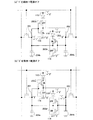
図12に本実施の形態で説明する不揮発性を有する半導体記憶装置のブロック図を示す。図12に示す半導体記憶装置1200は、デコーダ1201と、書き込み読み出し回路1202と、メモリセルアレイ1203と、から構成される。デコーダ1201は、第1の書き込みアドレス信号線1204と、第1の読み出しアドレス信号線1205と、第2の読み出しアドレス信号線1206と、ライトイネーブル信号線1207と、リードイネーブル信号線1225が接続される。またデコーダ1201は、複数のメモリセル1208と、ライトワード線1209、第1のリードワード線1210、及び第2のリードワード線1211を介して、接続される。書き込み読み出し回路1202は、ライトイネーブル信号線1207と、リードイネーブル信号線1225と、第2の書き込みアドレス信号線1212と、第3の読み出しアドレス信号線1213と、第4の読み出しアドレス信号線1214と、入力データ信号線1215と、第1の出力データ信号線1216と、第2の出力データ信号線1217が接続される。また書き込み読み出し回路1202は、複数のメモリセル1208と、ライトビット信号線1218と、ライトビット反転信号線1219と、第1のリードビット線1220、及び第2のリードビット線1221に接続される。また半導体記憶装置1200には、複数のメモリセルに、電源電位(H電位または高電位電源ともいう。また図中”1”と表記する。)及びグラウンド電位(L電位または低電位電源ともいう。また図中”0”と表記する。)を供給するための第1の電源制御回路1222a、第2の電源制御回路1222bを有している。第1の電源制御回路1222a及び第2の電源制御回路1222bと、複数のメモリセル1208は、メモリセル1208に電源電位を入力するための電源線1223と、グラウンド電位を入力するためのグラウンド線1224を介して、接続される。
FIG. 12 is a block diagram of a nonvolatile semiconductor memory device described in this embodiment. A
なお、本実施の形態において、ライトワード線とは、メモリセルのデータの書き込みを行うためのワード線のことをいう。またリードワード線とは、メモリセルのデータの読み出しを行うためのワード線のことをいう。また、ライトビット線及びライトビット反転信号線とは、メモリセルのデータの書き込みを行うためのビット線及びビット反転信号線のことをいう。また、リードビット線とは、メモリセルのデータの読み出しを行うためのビット線のことをいう。 Note that in this embodiment mode, a write word line refers to a word line for writing data in a memory cell. The read word line refers to a word line for reading data from a memory cell. The write bit line and the write bit inversion signal line are a bit line and a bit inversion signal line for writing data in the memory cell. The read bit line refers to a bit line for reading data from a memory cell.
なお、本実施の形態では、半導体記憶装置1200に、第1の電源制御回路1222a、第2の電源制御回路1222bを2つ配置する構成としたが、いずれか一方であればよい。図12に示すように、メモリセルアレイ1203の両側より、電源電位及びグラウンド電位を供給する構成とすることによって、より確実に複数のメモリセルに、所望の電位を供給することができる。
Note that in this embodiment mode, the first power
なお、図12に示した半導体記憶装置が、上記実施の形態2の図7で示した半導体記憶装置と異なる点は、メモリセルからのデータの読み出しを行うための配線として、第1のリードワード線1210及び第2のリードワード線1211、並びに第1のリードビット線1220と、第2のリードビット線1221を用いる点である。データの読み出しを行う配線を複数設けることによって、メモリセルからのデータの読み出しを、高速に行うことのできる半導体記憶装置とすることができる。
Note that the semiconductor memory device shown in FIG. 12 is different from the semiconductor memory device shown in FIG. 7 of Embodiment 2 in that the first read word is used as a wiring for reading data from the memory cell. The
図12において、メモリセル1208は、1ビットの値を保持することができる。そして、メモリセルアレイ1203はメモリセル1208を(ビット数)×(ライン数)の個数分有する。
In FIG. 12, a
書き込み読み出し回路1202は半導体記憶装置1200の外部から入力データ信号線1215から入力されるデータをメモリセルアレイ1203の各メモリセル1208に書き込む処理と、メモリセルアレイ1203の各メモリセル1208からデータを読み出して第1の出力データ信号線1216と、第2の出力データ信号線1217によってメモリの外部にデータを送信する処理を行う。
The write /
デコーダ1201は半導体記憶装置1200の外部から、第1の書き込みアドレス信号線1204、第1の読み出しアドレス信号線1205、第2の読み出しアドレス信号線1206より入力されるアドレスに応じて、ライトワード線1209、第1のリードワード線1210、または第2のリードワード線1211に信号を出力する。
The
デコーダ1201はライトワード線1209、第1のリードワード線1210、または第2のリードワード線1211へ信号を出力し、各メモリセル1208でのデータの読み出しまたは書き込みを制御する。例えば、書き込み時には、ライトワード線1209の一つが高電位の状態(以下、「H電位」と記す。また図中”1”と表記する。)となり、読み出し時には第1のリードワード線1210及び第2のリードワード線1211の一つがH電位となる。なお、ライトワード線1209、第1のリードワード線1210、及び第2のリードワード線1211が選択されない状態ではグラウンド電位の状態(以下、「L電位」と記す。また図中”0”と表記する。)となる。
The
ライトビット信号線1218及びライトビット反転信号線1219は、それぞれ書き込み用のビット線である。書き込み時には外部からのデータがライトビット信号線1218及びライトビット反転信号線1219に入力される。また第1のリードビット線1220及び第2のリードビット線1221は、読み出し用のビット線である。読み出し時には、書き込み読み出し回路1202によりプリチャージした上で、アドレスによって選択されたメモリセルのデータに基づいて変化する第1のリードビット線1220及び第2のリードビット線1221の電位を読み取る。
The write
このような半導体記憶装置1200によって、ビット数及びライン数に応じた情報を記憶することができる。
Such a
また本実施形態にで示すメモリセルおいては、上記実施の形態2と同様に、インバーター回路を略記した図8(b)に示すような回路図で表記することとする。 Further, in the memory cell shown in this embodiment, as in the second embodiment, a circuit diagram as shown in FIG. 8B in which the inverter circuit is abbreviated is shown.
次に図13で、図12のメモリセル1208の回路図について説明する。図13に示す本実施の形態のメモリセル1208は、図12でも示したように、ライトワード線1209、第1のリードワード線1210、または第2のリードワード線1211、ライトビット信号線1218、ライトビット反転信号線1219、第1のリードビット線1220、第2のリードビット線1221、電源線1223、及びグラウンド線1224に接続される。メモリセル1208は、第1のNチャネル型トランジスタ1301a(第1のトランジスタともいう)、第2のNチャネル型トランジスタ1301b(第2のトランジスタともいう)、ラッチ回路1302、ダイオード1303、第3のNチャネル型トランジスタ1304(第3のトランジスタともいう)、第4のNチャネル型トランジスタ1305(第4のトランジスタともいう)、第5のNチャネル型トランジスタ1306(第5のトランジスタともいう)、第6のNチャネル型トランジスタ1307(第6のトランジスタともいう)、を有する。ラッチ回路1302は、第1のインバーター回路1302a、第2のインバーター回路1302bを有する。
Next, a circuit diagram of the
図13において、第1のNチャネル型トランジスタ1301aは、ライトワード線1209の電位に基づいて、ライトビット信号線1218の電位をラッチ回路1302に入力するかを切り替えるスイッチとしての機能を有する。また第2のNチャネル型トランジスタ1301bは、ライトワード線1209の電位に基づいて、ライトビット反転信号線1219の電位をラッチ回路1302に入力するかを切り替えるスイッチとしての機能を有する。また、ダイオード1303は、電源線1223からの電源電位をラッチ回路1302に供給し、且つラッチ回路1302から電荷のリークのないようにする機能を有する。
In FIG. 13, the first N-
また第3のNチャネル型トランジスタ1304は、ゲート端子に接続されたラッチ回路1302の一方のノード(第1のインバーター回路1302aの出力端子)の電位をゲート容量で保持し、且つゲート端子に印加される電位に応じて第1のリードビット線1220と第4のNチャネル型トランジスタ1305との電気的な接続を切り替える機能を有する。一例として図13においては、第3のNチャネル型トランジスタ1304は、第1端子が第1のリードビット線1220に接続され、第2端子が第4のNチャネル型トランジスタ1305の第2端子に接続されている。
The third N-
また第4のNチャネル型トランジスタ1305は、ゲート端子に接続された第1のリードワード線1210の電位に応じて、第3のNチャネル型トランジスタ1304とグラウンド線1224との電気的な接続を切り替える機能を有する。一例として図13においては、第4のNチャネル型トランジスタ1305は、第1端子がグラウンド線1224に接続され、第2端子が第3のNチャネル型トランジスタ1304の第2端子に接続されている。
The fourth N-
また第5のNチャネル型トランジスタ1306は、ゲート端子に接続されたラッチ回路1302の他方のノード(第1のインバーター回路1302bの出力端子)の電位をゲート容量で保持し、且つゲート端子に印加される電位に応じて第2のリードビット線1221と第6のNチャネル型トランジスタ1307との電気的な接続を切り替える機能を有する。一例として図13においては、第5のNチャネル型トランジスタ1306は、第1端子が第2のリードビット線1221に接続され、第2端子が第6のNチャネル型トランジスタ1307の第2端子に接続されている。
The fifth N-
また第6のNチャネル型トランジスタ1307は、ゲート端子に接続された第2のリードワード線1211の電位に応じて、第5のNチャネル型トランジスタ1306とグラウンド線1224との電気的な接続を切り替える機能を有する。一例として図13においては、第6のNチャネル型トランジスタ1307は、第1端子がグラウンド線1224に接続され、第2端子が第5のNチャネル型トランジスタ1306の第2端子に接続されている。
The sixth N-
なお本実施の形態において、図12のメモリセル1208に、データ「1」が書き込まれていること、またデータ「0」が書き込まれていることとは、上記実施の形態1でのメモリセル107へのデータの書き込みの説明と同様である。
Note that in this embodiment mode, data “1” is written in the
なお、図13で、メモリセル1308が不揮発性を有することで不揮発性の半導体記憶装置が得られる原理は、上記実施の形態1の図3乃至図5での説明と同様である。すなわち、図3乃至図5で説明した第2の容量素子204bが、図13の第3のNチャネル型トランジスタ1304のゲート容量に相当し、図3乃至図5で説明した第1の容量素子204aが、図13の第5のNチャネル型トランジスタ1306に相当する。そして、図3乃至図5で説明した第1の容量素子204a及び第2の容量素子204bと同様に、電源が切られることで電源線1223の電源電位がグラウンド電位に変わった場合にも、ダイオード1303によって電荷のリークを防いで電荷の保持をおこなうことができる。
Note that in FIG. 13, the principle that a nonvolatile semiconductor memory device is obtained when the
そこで本実施の形態では、異なるリードビット線である第1のリードビット線1220及び第2のリードビット線1221によって、メモリセル1308のデータの読み出しを複数同時に別に行う動作について図14(A)、(B)を用いて説明する。
Therefore, in this embodiment, an operation of simultaneously reading a plurality of data from the
図14(A)には、図13で説明したメモリセル1308について、同じライトワード線、第1のリードワード線、及び第2のリードワード線に接続された第1のメモリセル1308a及び第2のメモリセル1308bを示している。図14(A)において、第1のメモリセル1308a及び第2のメモリセル1308bのデータの読み出しについては、上記実施の形態2の図10で説明したメモリセルからのデータの読み出しと同様であるため説明を省略する。
14A shows the
本実施の形態に説明するメモリセルは、第1のリードワード線及び第2のリードワード線に接続され、そして第1のリードビット線及び第2のリードビット線にからデータを読み出すものである。そこで図14(B)で、第1のメモリセル1308a及び第2のメモリセル1308bのデータの読み出しについて例を示し、説明する。図14(B)に示す第1のメモリセル1308a及び第2のメモリセル1308bは、共に第1のリードビット線1220及び第2のリードビット線1221に接続されている。図14(B)において、第1のメモリセル1308a及び第2のメモリセル1308bに保持されているデータは、第1のリードビット線1220及び第2のリードビット線1221より、アナログスイッチ1401を介して読み出される。そのため、第1のメモリセル1308aのデータは、アナログスイッチ1401を制御して、第1のリードビット線1220より読み出し、同時に第2のメモリセル1308bのデータは、アナログスイッチ1401を制御して、第2のリードビット線1221より読み出すことができる。そのため、2つのメモリセルからのデータの読み出しを同時におこなうことができるため、データの読み出しの高速化を図ることができる。
The memory cell described in this embodiment is connected to the first read word line and the second read word line, and reads data from the first read bit line and the second read bit line. . Thus, an example of reading data from the
なお、図13及び図14で説明した第3のNチャネル型トランジスタ1304及び第4のNチャネル型トランジスタ1305、並びに第5のNチャネル型トランジスタ1305及び第6のNチャネル型トランジスタ1306は、メモリセルに保持されたデータが「1」または「0」であることを第1のリードビット線1220及び第2のリードビット線1221で読み取ることができるように接続されていればよい。図15に図13で説明したメモリセルの回路図とは別の構成について示す。図15に示すメモリセルの回路図において、図13と異なる点は、第3のNチャネル型トランジスタ1304のゲート端子に第1のリードワード線1210が接続され、第4のNチャネル型トランジスタ1305のゲート端子に第1のインバーター回路1302aの出力端子が接続され、第5のNチャネル型トランジスタ1306のゲート端子に第2のリードワード線1211が接続され、第6のNチャネル型トランジスタ1307のゲート端子に第2のインバーター回路1302bの出力端子が接続され、点にある。図15に示すメモリセルにおいても、図13で説明した図14のメモリセルの回路図と同様に、第3のNチャネル型トランジスタ1304及び第4のNチャネル型トランジスタ1305が共にオンになる場合の第1のリードビット線1220の電位の変化を読み取ること、並びに第5のNチャネル型トランジスタ1306及び第6のNチャネル型トランジスタ1307が共にオンになる場合の第2のリードビット線1221の電位の変化を読み取ることで、メモリセル内のデータを読み出すことができる。
Note that the third N-
なお本実施の形態では、ダイオード1303をメモリセル毎に設ける構成について示したが、これに限定されない。ダイオードは、電源線毎に設ける構成であってもよい。電源線毎にダイオードを設ける構成とすることにより、メモリセルの小型化を図りつつ、且つ各メモリセルの不揮発性化を図ることができる。
Note that although a structure in which the
なお、本実施の形態で説明した半導体記憶装置のメモリセルは、メモリセルが有するダイオード及び第3のNチャネル型トランジスタ1304のゲート容量及び第5のNチャネル型トランジスタのゲート容量によって、実施の形態1で説明したように電源が切られた状態でもデータの保持ができる。メモリセルはデータ「1」またはデータ「0」のいずれかを保持すれば、再度電源線より電源電位が供給された場合に、第3のNチャネル型トランジスタ804のゲート容量のいずれかに保持された電荷に基づいて、メモリセルはデータを再度保持し続けることができる。
Note that the memory cell of the semiconductor memory device described in this embodiment mode includes the diodes included in the memory cell, the gate capacitance of the third N-
また、本実施形態で説明した半導体記憶装置のメモリセルでは、上記実施の形態1で説明したメモリセルの構成と同様に、ラッチ回路に供給する電源線からの電源電位を常時供給することなく、データの保持をおこなうことが可能となる。そのため、本実施形態で説明した半導体記憶装置のメモリセルでは、データの保持を行う上で、一定期間毎に電源電位の供給を行う構成とすればよいため、消費電力を低減することができる。加えて、メモリセルからのデータの読み出しと、メモリセルへのデータの書き込みを行う配線を別に設けることができるため、データの読み出しと書き込みをより確実に、且つ高速に行うことのできる半導体記憶装置を得ることができる。またさらに、メモリセルからのデータの読み出しを複数の配線を用いて行うことにより、データの読み出しを高速に行うことのできる半導体記憶装置を得ることができる。
Further, in the memory cell of the semiconductor memory device described in this embodiment, as in the configuration of the memory cell described in
なお、本実施の形態は、本明細書の実施の形態の技術的要素と組み合わせて行うことができる。
(実施の形態4)
Note that this embodiment mode can be implemented in combination with the technical elements of the embodiment modes in this specification.
(Embodiment 4)
本発明の半導体記憶装置は、中央演算装置(CPU)に適用することができる。本実施の形態では、本発明の半導体記憶装置を搭載したCPUの構成について説明する。CPUの簡単な構成を図16に示す。 The semiconductor memory device of the present invention can be applied to a central processing unit (CPU). In this embodiment mode, a structure of a CPU on which the semiconductor memory device of the present invention is mounted will be described. A simple configuration of the CPU is shown in FIG.
CPUは、D$ブロック(データキャッシュ:以下D$1601)、I$ブロック(インストラクションキャッシュ:以下I$1602)、DUブロック(データユニット:以下DU1603)、ALUブロック(Arithmetic Logic Unit,算術論理演算回路:以下ALU1604)、PCブロック(プログラムカウンター:PC1605)、IOブロック(InOut:以下IO1606)を有する。 The CPU includes a D $ block (data cache: hereinafter D $ 1601), an I $ block (instruction cache: hereinafter I $ 1602), a DU block (data unit: hereinafter DU1603), an ALU block (Arithmatic Logic Unit, an arithmetic logic circuit) : ALU 1604), PC block (program counter: PC 1605), and IO block (InOut: IO 1606).
D$1601は最近アクセスされたアドレスのデータを一時的に保持しそのアドレスのデータに高速でアクセスできるようにする機能を有するものである。I$1602は最近アクセスされたアドレスの命令を一時的に保持しそのアドレスの命令に高速でアクセスできるようにする機能を有するものである。DU1603はストア又はロード命令が実行された時、D$1601にアクセスするか、IOにアクセスするかを決定する機能を有するものである。ALU1604は算術論理演算回路であり、四則演算、比較演算、論理演算などを行う機能を有するものである。PC1605は、現在実行中の命令のアドレスを保持し、その実行終了後、次の命令をフェッチする機能を有する。又、次の命令をフェッチする時にI$1602にアクセスするか、IO1606にアクセスするかを決定する機能を有するものである。IO1606はDU1603、PC1605からのアクセスを受け外部とデータの送受信を行う機能を有するものである。以下にそれぞれの関係を説明する。
The D $ 1601 has a function of temporarily holding data at the recently accessed address so that the address data can be accessed at high speed. The I $ 1602 has a function of temporarily holding an instruction at a recently accessed address so that the instruction at the address can be accessed at high speed. The
PC1605が命令をフェッチする時に、はじめにI$1602にアクセスし、I$1602に該当するアドレスの命令がない場合にIO1606にアクセスする。これによって得られた命令はI$1602に格納すると共に実行を行う。実行すべき命令が算術論理演算の場合はALU1604が演算を行う。実行すべき命令がストア又はロード命令の場合は、DU1603が演算を行う。この際、DU1603はまずD$1601にアクセスし、該当するアドレスのデータがD$1601にない場合にIO1606にアクセスする。
When the
このようなCPUにおいて、本発明の半導体記憶装置は、D$1601とI$1602、ALU1604の内部に存在するレジスタに適用することができる。その結果、不揮発性を達成した半導体記憶回路を有するCPUを提供することができ、電源が切れた状態でもデータの保持ができるため、低消費電力化を図ることができる。また、実施の形態3で示した半導体記憶装置を用いることで高速にデータの読み出しが可能な不揮発性を有する半導体記憶装置を具備するCPUとすることもできる。 In such a CPU, the semiconductor memory device of the present invention can be applied to registers existing in D $ 1601, I $ 1602, and ALU1604. As a result, a CPU having a nonvolatile semiconductor memory circuit can be provided, and data can be retained even when the power is turned off, so that power consumption can be reduced. Further, by using the semiconductor memory device described in Embodiment 3, a CPU including a nonvolatile semiconductor memory device that can read data at high speed can be used.
なお、本実施の形態は、本明細書の実施の形態の技術的要素と組み合わせて行うことができる。
(実施の形態5)
Note that this embodiment mode can be implemented in combination with the technical elements of the embodiment modes in this specification.
(Embodiment 5)
本実施の形態では、上記実施の形態で説明した半導体記憶装置を具備するRFIDタグ(以下、半導体装置という。IDチップ、ICタグ、IDタグ、RFタグ、無線タグ、電子タグ、トランスポンダともいわれる)の構成について説明する。 In this embodiment, an RFID tag including the semiconductor memory device described in the above embodiment (hereinafter referred to as a semiconductor device; also referred to as an ID chip, an IC tag, an ID tag, an RF tag, a wireless tag, an electronic tag, or a transponder) The configuration of will be described.
半導体装置の構成について、図17を用いて説明する。図17は半導体装置内のブロック図である。半導体装置1700は、アンテナ1702及び半導体集積回路1701を有する。そして、半導体集積回路1701は、送受信回路1703、電源回路1704、制御回路1705、記憶素子1706を有する。
A structure of the semiconductor device is described with reference to FIGS. FIG. 17 is a block diagram in the semiconductor device. A semiconductor device 1700 includes an
次に、半導体装置の動作について、図17及び図18を用いて説明する。図18に示すように、制御用端末1722に無線通信装置(以下、通信装置1720という。またリーダライタ、リーダ/ライタ、コントローラ、インテロゲータ、質問器ともいわれる)を介して接続されたアンテナユニット1721から搬送波を変調した無線信号が送信される。ここで、無線信号には通信装置1720から半導体装置1700への命令が含まれている。 Next, operation of the semiconductor device will be described with reference to FIGS. As shown in FIG. 18, from an antenna unit 1721 connected to a control terminal 1722 via a wireless communication device (hereinafter referred to as a communication device 1720. Also referred to as a reader / writer, a reader / writer, a controller, an interrogator, or an interrogator). A radio signal with a modulated carrier wave is transmitted. Here, the radio signal includes a command from the communication device 1720 to the semiconductor device 1700.
図17において、半導体装置1700が有するアンテナ1702は当該無線信号を受信する。そして、受信された当該無線信号はアンテナ1702に接続された送受信回路1703を介して各回路ブロックに送られる。送受信回路1703には電源回路1704、制御回路1705、及び記憶素子1706が接続されている。
In FIG. 17, an
送受信回路1703の整流機能により第1の高電源電位(VDD1)、電源回路1704より第2の高電源電位(VDD2)が生成される。本実施の形態においては、生成された2つの高電源電位のうち、第2の高電源電位VDD2が半導体集積回路1701の各回路ブロックに供給されるものとする。なお、本実施の形態において、低電源電位(VSS)は共通である。図17において、電源回路1704は、定電圧回路で構成される。
A first high power supply potential (VDD1) is generated by the rectifying function of the transmission /
送受信回路1703の整流機能と電源回路1704の動作について簡単に説明する。例えば、送受信回路1703の整流機能として、一つの整流回路で構成し、電源回路1704として、定電圧回路で構成した場合を考える。ここで、整流機能をはたす整流回路として、ダイオード及び容量素子を用いることができる。アンテナ1702を介して送受信回路1703に送られた当該無線信号は、整流回路に入力され、整流される。そして、整流回路の容量素子により平滑化され、第1の高電源電位(VDD1)が生成される。生成されたVDD1は、定電圧回路を通ることで、入力以下の安定した電圧(第2の高電源電位、VDD2)になる。定電圧回路の出力電圧であるVDD2が電源として各回路ブロックに供給される。なお、生成されたVDD1を電源として各回路ブロックに供給してもよい。さらに、VDD1及びVDD2の両方を各回路ブロックに供給してもよい。各回路ブロックの動作条件及び用途によりVDD1またはVDD2の供給を使い分けることが望ましい。
The rectification function of the transmission /
図17に示す半導体装置で、定電圧回路は直流電圧をほぼ一定に保つ機能を有しており、電圧や電流または両方により直流電圧をほぼ一定に保つことができる回路であればどのような回路でもよい。 In the semiconductor device shown in FIG. 17, the constant voltage circuit has a function of keeping the DC voltage substantially constant, and any circuit can be used as long as the circuit can keep the DC voltage substantially constant by voltage, current, or both. But you can.
また、送受信回路1703の復調機能より復調信号1709が生成される。生成された復調信号1709が各回路ブロックに供給される。送受信回路1703と制御回路1705は接続されており、送受信回路1703で生成された復調信号1709が制御回路1705に供給される。
Further, a demodulated signal 1709 is generated by the demodulating function of the transmission /
制御回路1705は、リセット回路を有する。リセット回路ではリセット信号が生成される。リセット信号は、半導体装置1700の初期化を行う信号である。 The control circuit 1705 has a reset circuit. A reset signal is generated in the reset circuit. The reset signal is a signal for initializing the semiconductor device 1700.
また、制御回路1705は、クロック生成回路を有する。クロック生成回路では送受信回路1703を介して送られてきた復調信号1709を元に、基本クロック信号を生成している。クロック生成回路にて生成された基本クロック信号は、制御回路内の回路で用いられる。
The control circuit 1705 includes a clock generation circuit. The clock generation circuit generates a basic clock signal based on the demodulated signal 1709 sent via the transmission /
さらに、制御回路1705は、送受信回路1703を介して送られてきた復調信号1709から、前記通信装置1720から半導体装置1700へ送られた命令を抽出し、どのような命令が送られてきたのかを判別する。また制御回路1705は、記憶素子1706を制御する役割も有している。
Further, the control circuit 1705 extracts a command sent from the communication device 1720 to the semiconductor device 1700 from the demodulated signal 1709 sent via the transmission /
こうして、通信装置1720からどのような命令が送られてきたのかを判別し、判別された命令により、記憶素子1706を動作させる。そして、記憶素子1706に記憶されたデータを含んだ信号、または、書き込まれた識別番号等の記憶データを含んだ信号を出力する。または、記憶素子1706に通信装置1720から送られてきた情報を記憶する。 In this manner, what command is sent from the communication device 1720 is determined, and the memory element 1706 is operated according to the determined command. Then, a signal including data stored in the memory element 1706 or a signal including stored data such as a written identification number is output. Alternatively, information transmitted from the communication device 1720 is stored in the storage element 1706.
ここで記憶素子1706は、上記実施の形態で説明した不揮発性を有する記憶素子1706を用いることができ、電源が切れた状態でもデータの保持ができるため、低消費電力化を図ることができる。また、実施の形態3で示した半導体記憶装置を用いることで高速にデータの読み出しが可能な不揮発性を有する半導体記憶装置を具備するCPUとすることもできる。 Here, the memory element 1706 can use the nonvolatile memory element 1706 described in the above embodiment and can hold data even when the power is turned off, so that power consumption can be reduced. Further, by using the semiconductor memory device described in Embodiment 3, a CPU including a nonvolatile semiconductor memory device that can read data at high speed can be used.
制御回路1705は記憶素子1706に記憶または書き込まれた識別番号等の固有データを含んだ信号を、ISO等の規格に則った符号化方式で符号化した信号に変える役割も有する。そして、符号化された信号1710にしたがって、送受信回路1703により、アンテナ1702に送られてきている信号に変調をかける。
The control circuit 1705 also has a role of changing a signal including unique data such as an identification number stored or written in the storage element 1706 into a signal encoded by an encoding method compliant with a standard such as ISO. Then, according to the encoded
変調をかけられた信号は、通信装置1720に接続されたアンテナユニット1721で受信される。そして、受信された信号は通信装置1720で解析され、半導体装置1700の識別番号等の固有データを認識することができる。 The modulated signal is received by the antenna unit 1721 connected to the communication device 1720. The received signal is analyzed by the communication device 1720 and unique data such as an identification number of the semiconductor device 1700 can be recognized.
本実施の形態で、半導体装置1700と通信装置1720との通信は、搬送波を変調することで行われる例について示した。なお搬送波は、125KHz、13.56MHz、950MHzなど規格により様々である。また変調の方式も規格により振幅変調、周波数変調、位相変調など様々な方式があるが、規格に即した変調方式であればどの変調方式を用いても良い。 In this embodiment, an example in which communication between the semiconductor device 1700 and the communication device 1720 is performed by modulating a carrier wave is described. The carrier wave varies depending on the standard such as 125 KHz, 13.56 MHz, and 950 MHz. There are various modulation methods such as amplitude modulation, frequency modulation, and phase modulation depending on the standard. Any modulation method may be used as long as the modulation method conforms to the standard.
信号の伝送方式は、搬送波の波長によって電磁結合方式、電磁誘導方式、マイクロ波方式など様々な種類に分類することができる。なお、半導体装置と通信装置との無線信号の送受信を長距離間で行う場合には、マイクロ波方式を選択することが望ましい。 The signal transmission method can be classified into various types such as an electromagnetic coupling method, an electromagnetic induction method, and a microwave method depending on the wavelength of the carrier wave. Note that when a radio signal is transmitted and received between a semiconductor device and a communication device over a long distance, it is desirable to select a microwave method.
なお、本実施の形態は、本明細書の実施の形態の技術的要素と組み合わせて行うことができる。
(実施の形態6)
Note that this embodiment mode can be implemented in combination with the technical elements of the embodiment modes in this specification.
(Embodiment 6)
本実施の形態では、上記実施の形態で述べた半導体記憶装置を構成するトランジスタの作製例について説明する。本実施の形態では特に、絶縁基板上に形成された半導体膜によりトランジスタを作製し、半導体記憶装置を具備する半導体装置とする形態について説明する。 In this embodiment, an example of manufacturing a transistor included in the semiconductor memory device described in the above embodiment will be described. In this embodiment mode, a mode in which a transistor is manufactured using a semiconductor film formed over an insulating substrate and a semiconductor memory device is provided will be described.
基板1901の一表面に剥離層1902を形成し、続けて下地となる絶縁膜1903および非晶質半導体膜1904(例えば非晶質珪素を含む膜)を形成する(図19(A))。剥離層1902、絶縁膜1903および非晶質半導体膜1904は、連続して形成することができる。連続して形成することにより、大気に曝されないため不純物の混入を防ぐことができる。
A
基板1901は、ガラス基板、石英基板、金属基板やステンレス基板、本工程の処理温度に耐えうる耐熱性があるプラスチック基板等を用いるとよい。このような基板であれば、その面積や形状に大きな制限はないため、例えば、1辺が1メートル以上であって、矩形状のものを用いれば、生産性を格段に向上させることができる。このような利点は、円形のシリコン基板を用いる場合と比較すると、大きな優位点である。従って、シリコン基板と比較して集積回路部やアンテナを大きく形成した場合であっても、低コスト化を実現することができる。
As the
なお、本工程では、剥離層1902を基板1901の全面に設けているが、必要に応じて、基板1901の全面に剥離層を設けた後に、フォトリソグラフィ法により剥離層1902を選択的に設けてもよい。また、基板1901に接するように剥離層1902を形成しているが、必要に応じて、基板1901に接するように酸化珪素(SiOx)膜、酸化窒化珪素(SiOxNy)(x>y)膜、窒化珪素(SiNx)膜、窒化酸化珪素(SiNxOy)(x>y)膜等の絶縁膜を形成し、当該絶縁膜に接するように剥離層1902を形成してもよい。
Note that although the
剥離層1902は、金属膜や金属膜と金属酸化膜の積層構造等を用いることができる。金属膜としては、タングステン(W)、モリブデン(Mo)、チタン(Ti)、タンタル(Ta)、ニオブ(Nb)、ニッケル(Ni)、コバルト(Co)、ジルコニウム(Zr)、亜鉛(Zn)、ルテニウム(Ru)、ロジウム(Rh)、パラジウム(Pd)、オスミウム(Os)、イリジウム(Ir)から選択された元素または前記元素を主成分とする合金材料若しくは化合物材料からなる膜を単層又は積層して形成する。また、これらの材料は、スパッタリング法やプラズマCVD法等の各種CVD法等を用いて形成することができる。金属膜と金属酸化膜の積層構造としては、上述した金属膜を形成した後に、酸素雰囲気化またはN2O雰囲気下におけるプラズマ処理、酸素雰囲気化またはN2O雰囲気下における加熱処理を行うことによって、金属膜表面に当該金属膜の酸化物または酸化窒化物を設けることができる。また、金属膜を形成した後に、オゾン水等の酸化力の強い溶液で表面を処理することにより、金属膜表面に当該金属膜の酸化物又は酸化窒化物を設けることができる。
For the
絶縁膜1903は、スパッタリング法やプラズマCVD法等により、珪素の酸化物または珪素の窒化物を含む膜を、単層又は積層で形成する。下地となる絶縁膜が2層構造の場合、例えば、1層目として窒化酸化珪素膜を形成し、2層目として酸化窒化珪素膜を形成するとよい。下地となる絶縁膜が3層構造の場合、1層目の絶縁膜として酸化珪素膜を形成し、2層目の絶縁膜として窒化酸化珪素膜を形成し、3層目の絶縁膜として酸化窒化珪素膜を形成するとよい。または、1層目の絶縁膜として酸化窒化珪素膜を形成し、2層目の絶縁膜として窒化酸化珪素膜を形成し、3層目の絶縁膜として酸化窒化珪素膜を形成するとよい。下地となる絶縁膜は、基板1901からの不純物の侵入を防止するブロッキング膜として機能する。
The insulating
半導体膜1904は、スパッタリング法、LPCVD法、プラズマCVD法等により、25〜200nm(好ましくは30〜150nm)の厚さで形成する。半導体膜1904としては、例えば、非晶質珪素膜を形成すればよい。
The
次に、非晶質の半導体膜1904にレーザー光を照射して結晶化を行う。なお、レーザー光の照射と、RTA又はファーネスアニール炉を用いる熱結晶化法、結晶化を助長する金属元素を用いる熱結晶化法とを組み合わせた方法等により非晶質の半導体膜1904の結晶化を行ってもよい。その後、得られた結晶質半導体膜を所望の形状にエッチングして、半導体膜1904a〜1904dを形成し、当該半導体膜1904a〜1904dを覆うようにゲート絶縁膜1905を形成する(図19(B))。
Next, crystallization is performed by irradiating the
半導体膜1904a〜1904dの作製工程の一例を以下に簡単に説明すると、まず、プラズマCVD法を用いて、膜厚50〜60nmの非晶質半導体膜(例えば、非晶質珪素膜)を形成する。次に、結晶化を助長する金属元素であるニッケルを含む溶液を非晶質半導体膜上に保持させた後、非晶質半導体膜に脱水素化の処理(500℃、1時間)と、熱結晶化の処理(550℃、4時間)を行って結晶質半導体膜を形成する。その後、レーザー発振器からレーザー光を照射し、フォトリソグラフィ法を用いることよって半導体膜1904a〜1904dを形成する。なお、結晶化を助長する金属元素を用いる熱結晶化を行わずに、レーザー光の照射だけで非晶質半導体膜の結晶化を行ってもよい。
An example of a manufacturing process of the
レーザー発振器としては、連続発振型のレーザービーム(CWレーザービーム)やパルス発振型のレーザービーム(パルスレーザービーム)を用いることができる。ここで用いることができるレーザービームは、Arレーザー、Krレーザー、エキシマレーザーなどの気体レーザー、単結晶のYAG、YVO4、フォルステライト(Mg2SiO4)、YAlO3、GdVO4、若しくは多結晶(セラミック)のYAG、Y2O3、YVO4、YAlO3、GdVO4に、ドーパントとしてNd、Yb、Cr、Ti、Ho、Er、Tm、Taのうち1種または複数種添加されているものを媒質とするレーザー、ガラスレーザー、ルビーレーザー、アレキサンドライトレーザー、Ti:サファイアレーザー、銅蒸気レーザーまたは金蒸気レーザーのうち一種または複数種から発振されるものを用いることができる。このようなレーザービームの基本波、及びこれらの基本波の第2高調波から第4高調波のレーザービームを照射することで、大粒径の結晶を得ることができる。例えば、Nd:YVO4レーザー(基本波1064nm)の第2高調波(532nm)や第3高調波(355nm)を用いることができる。このときレーザーのパワー密度は0.01〜100MW/cm2程度(好ましくは0.1〜10MW/cm2)が必要である。そして、走査速度を10〜2000cm/sec程度として照射する。なお、単結晶のYAG、YVO4、フォルステライト(Mg2SiO4)、YAlO3、GdVO4、若しくは多結晶(セラミック)のYAG、Y2O3、YVO4、YAlO3、GdVO4に、ドーパントとしてNd、Yb、Cr、Ti、Ho、Er、Tm、Taのうち1種または複数種添加されているものを媒質とするレーザー、Arイオンレーザー、またはTi:サファイアレーザーは、連続発振をさせることが可能であり、Qスイッチ動作やモード同期などを行うことによって10MHz以上の発振周波数でパルス発振をさせることも可能である。10MHz以上の発振周波数でレーザービームを発振させると、半導体膜がレーザーによって溶融してから固化するまでの間に、次のパルスが半導体膜に照射される。従って、発振周波数が低いパルスレーザーを用いる場合と異なり、半導体膜中において固液界面を連続的に移動させることができるため、走査方向に向かって連続的に成長した結晶粒を得ることができる。 As the laser oscillator, a continuous wave laser beam (CW laser beam) or a pulsed laser beam (pulse laser beam) can be used. The laser beam that can be used here is a gas laser such as Ar laser, Kr laser, or excimer laser, single crystal YAG, YVO 4 , forsterite (Mg 2 SiO 4 ), YAlO 3 , GdVO 4 , or polycrystalline ( Ceramic) YAG, Y 2 O 3 , YVO 4 , YAlO 3 , GdVO 4 with one or more of Nd, Yb, Cr, Ti, Ho, Er, Tm, Ta added as dopants Lasers oscillated from one or more of laser, glass laser, ruby laser, alexandrite laser, Ti: sapphire laser, copper vapor laser, or gold vapor laser as a medium can be used. By irradiating the fundamental wave of such a laser beam and the second to fourth harmonics of these fundamental waves, a crystal having a large grain size can be obtained. For example, the second harmonic (532 nm) or the third harmonic (355 nm) of an Nd: YVO 4 laser (fundamental wave 1064 nm) can be used. In this case, a laser power density is about 0.01 to 100 MW / cm 2 (preferably 0.1 to 10 MW / cm 2) is required. Then, irradiation is performed at a scanning speed of about 10 to 2000 cm / sec. Note that single crystal YAG, YVO 4 , forsterite (Mg 2 SiO 4 ), YAlO 3 , GdVO 4 , or polycrystalline (ceramic) YAG, Y 2 O 3 , YVO 4 , YAlO 3 , GdVO 4 , dopants Nd, Yb, Cr, Ti, Ho, Er, Tm, Ta as a medium, a laser, Ar ion laser, or Ti: sapphire laser with one or more added as a medium should be continuously oscillated It is also possible to perform pulse oscillation at an oscillation frequency of 10 MHz or more by performing Q switch operation, mode synchronization, or the like. When a laser beam is oscillated at an oscillation frequency of 10 MHz or higher, the semiconductor film is irradiated with the next pulse during the period from when the semiconductor film is melted by the laser to solidification. Therefore, unlike the case of using a pulse laser having a low oscillation frequency, the solid-liquid interface can be continuously moved in the semiconductor film, so that crystal grains continuously grown in the scanning direction can be obtained.
次に、半導体膜1904a〜半導体膜1904dを覆うゲート絶縁膜1905を形成する。ゲート絶縁膜1905は、CVD法やスパッタリング法等により、珪素の酸化物又は珪素の窒化物を含む膜を、単層又は積層して形成する。具体的には、酸化珪素膜、酸化窒化珪素膜、窒化酸化珪素膜を、単層又は積層して形成する。
Next, a
また、ゲート絶縁膜1905は、非晶質の半導体膜1904a〜半導体膜1904dに対し高密度プラズマ処理を行い、表面を酸化又は窒化することで形成しても良い。例えば、He、Ar、Kr、Xeなどの希ガスと、酸素、酸化窒素(NO2)、アンモニア、窒素、水素などの混合ガスを導入したプラズマ処理で形成する。この場合のプラズマの励起は、マイクロ波の導入により行うと、低電子温度で高密度のプラズマを生成することができる。この高密度プラズマで生成された酸素ラジカル(OHラジカルを含む場合もある)や窒素ラジカル(NHラジカルを含む場合もある)によって、半導体膜の表面を酸化又は窒化することができる。
Alternatively, the
このような高密度プラズマを用いた処理により、1〜20nm、代表的には5〜10nmの絶縁膜が半導体膜に形成される。この場合の反応は、固相反応であるため、当該絶縁膜と半導体膜との界面準位密度はきわめて低くすることができる。このような、高密度プラズマ処理は、半導体膜(結晶性シリコン、或いは多結晶シリコン)を直接酸化(若しくは窒化)するため、形成される絶縁膜の厚さは理想的には、ばらつきをきわめて小さくすることができる。加えて、結晶性シリコンの結晶粒界でも酸化が強くされることがないため、非常に好ましい状態となる。すなわち、ここで示す高密度プラズマ処理で半導体膜の表面を固相酸化することにより、結晶粒界において異常に酸化反応をさせることなく、均一性が良く、界面準位密度が低い絶縁膜を形成することができる。 By such treatment using high-density plasma, an insulating film with a thickness of 1 to 20 nm, typically 5 to 10 nm, is formed over the semiconductor film. Since the reaction in this case is a solid-phase reaction, the interface state density between the insulating film and the semiconductor film can be extremely low. Such high-density plasma treatment directly oxidizes (or nitrides) a semiconductor film (crystalline silicon or polycrystalline silicon), so that the thickness of the formed insulating film ideally has extremely small variation. can do. In addition, since oxidation is not strengthened even at the crystal grain boundaries of crystalline silicon, a very favorable state is obtained. That is, the surface of the semiconductor film is solid-phase oxidized by the high-density plasma treatment shown here, thereby forming an insulating film with good uniformity and low interface state density without causing an abnormal oxidation reaction at the grain boundaries. can do.
ゲート絶縁膜1905は、高密度プラズマ処理によって形成される絶縁膜のみを用いても良いし、それに加えてプラズマや熱反応を利用したCVD法で酸化シリコン、酸窒化シリコン、窒化シリコンなどの絶縁膜を堆積し、積層させても良い。いずれにしても、高密度プラズマで形成した絶縁膜をゲート絶縁膜の一部又は全部に含んで形成されるトランジスタは、特性のばらつきを小さくすることができる。
As the
また、半導体膜に対し、連続発振レーザー光若しくは10MHz以上の周波数で発振するレーザー光を照射しながら一方向に走査して結晶化させて得られた半導体膜1904a〜1904dは、そのレーザー光の走査方向に結晶が成長する特性がある。その走査方向をチャネル長方向(チャネル形成領域が形成されたときにキャリアが流れる方向)に合わせてトランジスタを配置し、上記ゲート絶縁層を組み合わせることで、特性ばらつきが小さく、しかも電界効果移動度が高い薄膜トランジスタ(TFT)を得ることができる。
In addition, the
次に、ゲート絶縁膜1905上に、第1の導電膜と第2の導電膜とを積層して形成する。ここでは、第1の導電膜は、プラズマCVD法やスパッタ法等により、20〜100nmの厚さで形成する。第2の導電膜は、100〜400nmの厚さで形成する。第1の導電膜と第2の導電膜は、タンタル(Ta)、タングステン(W)、チタン(Ti)、モリブデン(Mo)、アルミニウム(Al)、銅(Cu)、クロム(Cr)、ニオブ(Nb)等から選択された元素又はこれらの元素を主成分とする合金材料若しくは化合物材料で形成する。または、リン等の不純物元素をドーピングした多結晶珪素に代表される半導体材料により形成する。第1の導電膜と第2の導電膜の組み合わせの例を挙げると、窒化タンタル膜とタングステン膜、窒化タングステン膜とタングステン膜、窒化モリブデン膜とモリブデン膜等が挙げられる。タングステンや窒化タンタルは、耐熱性が高いため、第1の導電膜と第2の導電膜を形成した後に、熱活性化を目的とした加熱処理を行うことができる。また、2層構造ではなく、3層構造の場合は、モリブデン膜とアルミニウム膜とモリブデン膜の積層構造を採用するとよい。
Next, a first conductive film and a second conductive film are stacked over the
次に、フォトリソグラフィ法を用いてレジストからなるマスクを形成し、ゲート電極とゲート配線を形成するためのエッチング処理を行って、半導体膜1904a〜1904dの上方にゲート電極1907を形成する。
Next, a resist mask is formed by photolithography, and an etching process for forming a gate electrode and a gate wiring is performed, so that a
次に、フォトリソグラフィ法により、レジストからなるマスクを形成して、半導体膜1904a〜1904dに、イオンドープ法またはイオン注入法により、n型を付与する不純物元素を低濃度に添加する。n型を付与する不純物元素は、15族に属する元素を用いれば良く、例えばリン(P)、砒素(As)を用いる。
Next, a resist mask is formed by photolithography, and an impurity element imparting n-type conductivity is added to the
次に、ゲート絶縁膜1905とゲート電極1907を覆うように、絶縁膜を形成する。絶縁膜は、プラズマCVD法やスパッタ法等により、珪素、珪素の酸化物又は珪素の窒化物の無機材料を含む膜や、有機樹脂などの有機材料を含む膜を、単層又は積層して形成する。次に、絶縁膜を、垂直方向を主体とした異方性エッチングにより選択的にエッチングして、ゲート電極1907の側面に接する絶縁膜1908(サイドウォールともよばれる)を形成する。絶縁膜1908は、後にLDD(Lightly Doped drain)領域を形成する際のドーピング用のマスクとして用いる。
Next, an insulating film is formed so as to cover the
次に、フォトリソグラフィ法により形成したレジストからなるマスクと、ゲート電極1907および絶縁膜1908をマスクとして用いて、半導体膜1904a〜1904dにn型を付与する不純物元素を添加して、チャネル形成領域1906aと、第1の不純物領域1906bと、第2の不純物領域1906cを形成する(図19(C))。第1の不純物領域1906bは薄膜トランジスタのソース領域又はドレイン領域として機能し、第2の不純物領域1906cはLDD領域として機能する。第2の不純物領域1906cが含む不純物元素の濃度は、第1の不純物領域1906bが含む不純物元素の濃度よりも低い。
Next, an impurity element imparting n-type conductivity is added to the
続いて、ゲート電極1907、絶縁膜1908等を覆うように、絶縁膜を単層または積層して形成し、当該絶縁膜上に薄膜トランジスタのソース電極又はドレイン電極として機能する導電膜1931を形成する。その結果、薄膜トランジスタ1930a〜1930dを含む素子層1951が得られる(図19(D))。なお、薄膜トランジスタ等の素子は、領域1950の全面に設けた構成としても良いし、領域1950の一部(例えば、中心部)を除いた部分に設けた構成としても良い。
Next, an insulating film is formed as a single layer or a stacked layer so as to cover the
絶縁膜は、CVD法、スパッタリング法、SOG法、液滴吐出法、スクリーン印刷法等により、珪素の酸化物や珪素の窒化物等の無機材料、ポリイミド、ポリアミド、ベンゾシクロブテン、アクリル、エポキシ等の有機材料やシロキサン材料等により、単層または積層で形成する。ここでは、絶縁膜を2層で設けた例を示しており、1層目の絶縁膜1909として窒化酸化珪素膜で形成し、2層目の絶縁膜1910として酸化窒化珪素膜で形成することができる。
Insulating film is formed by CVD, sputtering, SOG, droplet discharge, screen printing, etc., inorganic materials such as silicon oxide and silicon nitride, polyimide, polyamide, benzocyclobutene, acrylic, epoxy, etc. A single layer or a stacked layer is formed using an organic material or a siloxane material. Here, an example in which an insulating film is provided in two layers is shown; a silicon nitride oxide film may be formed as the first insulating
なお、絶縁膜1909、1910を形成する前、または絶縁膜1909、1910のうちの一方又は両方を形成した後に、半導体膜1904a〜1904dの結晶性の回復や半導体膜に添加された不純物元素の活性化、半導体膜の水素化を目的とした加熱処理を行うとよい。加熱処理には、熱アニール、レーザーアニール法またはRTA法などを適用するとよい。
Note that before the insulating
導電膜1931は、フォトリソグラフィ法により絶縁膜1909、1910等をエッチングして、第1の不純物領域1906bを露出させるコンタクトホールを形成した後、コンタクトホールを充填するように導電膜を形成し、当該導電膜を選択的にエッチングして形成する。なお、導電膜を形成する前に、コンタクトホールにおいて露出した半導体膜1904a〜1904dの表面にシリサイドを形成してもよい。
The
また、導電膜1931は、CVD法やスパッタリング法等により、アルミニウム(Al)、タングステン(W)、チタン(Ti)、タンタル(Ta)、モリブデン(Mo)、ニッケル(Ni)、白金(Pt)、銅(Cu)、金(Au)、銀(Ag)、マンガン(Mn)、ネオジウム(Nd)、炭素(C)、シリコン(Si)から選択された元素、又はこれらの元素を主成分とする合金材料若しくは化合物材料で、単層又は積層で形成する。アルミニウムを主成分とする合金材料とは、例えば、アルミニウムを主成分としニッケルを含む材料、又は、アルミニウムを主成分とし、ニッケルと、炭素と珪素の一方又は両方とを含む合金材料に相当する。導電膜1931は、例えば、バリア膜とアルミニウムシリコン(Al−Si)膜とバリア膜の積層構造、バリア膜とアルミニウムシリコン(Al−Si)膜と窒化チタン(TiN)膜とバリア膜の積層構造を採用するとよい。なお、バリア膜とは、チタン、チタンの窒化物、モリブデン、又はモリブデンの窒化物からなる薄膜に相当する。アルミニウムやアルミニウムシリコンは抵抗値が低く、安価であるため、導電膜1931を形成する材料として最適である。また、上層と下層のバリア層を設けると、アルミニウムやアルミニウムシリコンのヒロックの発生を防止することができる。また、還元性の高い元素であるチタンからなるバリア膜を形成すると、結晶質半導体膜上に薄い自然酸化膜ができていたとしても、この自然酸化膜を還元し、結晶質半導体膜と良好なコンタクトをとることができる。
The
次に、導電膜1931を覆うように、絶縁膜1911を形成する(図20(A))。絶縁膜1911は、CVD法、スパッタリング法、SOG法、液滴吐出法またはスクリーン印刷法等を用いて、無機材料又は有機材料により、単層又は積層で形成する。また、絶縁膜1911は、好適には、0.75μm〜3μmの厚さで形成する。
Next, an insulating
次に、絶縁膜1911の表面にアンテナとして機能する導電膜1912を選択的に形成する(図20(B))。 Next, a conductive film 1912 functioning as an antenna is selectively formed over the surface of the insulating film 1911 (FIG. 20B).
導電膜1912は、フォトリソグラフィ法により絶縁膜1911をエッチングして、導電膜1931を露出させるコンタクトホールを形成した後、コンタクトホールを充填するように導電膜を形成し、当該導電膜を選択的にエッチングして形成する。
The conductive film 1912 is formed by etching the insulating
また導電膜1912は、CVD法、スパッタリング法、スクリーン印刷やグラビア印刷等の印刷法、メッキ処理等を用いて、導電性材料により形成すればよい。導電性材料は、アルミニウム(Al)、チタン(Ti)、銀(Ag)、銅(Cu)、金(Au)、白金(Pt)ニッケル(Ni)、パラジウム(Pd)、タンタル(Ta)、モリブデン(Mo)から選択された元素、又はこれらの元素を主成分とする合金材料若しくは化合物材料で、単層構造又は積層構造で形成する。 The conductive film 1912 may be formed using a conductive material by a CVD method, a sputtering method, a printing method such as screen printing or gravure printing, a plating process, or the like. Conductive materials are aluminum (Al), titanium (Ti), silver (Ag), copper (Cu), gold (Au), platinum (Pt) nickel (Ni), palladium (Pd), tantalum (Ta), molybdenum An element selected from (Mo) or an alloy material or a compound material containing these elements as a main component is formed in a single layer structure or a laminated structure.
例えば、スクリーン印刷法を用いてアンテナとして機能する導電膜1912を形成する場合には、粒径が数nmから数十μmの導電体粒子を有機樹脂に溶解または分散させた導電性のペーストを選択的に印刷することによって設けることができる。導電体粒子としては、銀(Ag)、金(Au)、銅(Cu)、ニッケル(Ni)、白金(Pt)、パラジウム(Pd)、タンタル(Ta)、モリブデン(Mo)およびチタン(Ti)等のいずれか一つ以上の金属粒子やハロゲン化銀の微粒子、または分散性ナノ粒子を用いることができる。スクリーン印刷法を用いて形成することにより、工程の簡略化が可能となり低コスト化を図ることができる。 For example, when the conductive film 1912 functioning as an antenna is formed using a screen printing method, a conductive paste in which conductive particles having a particle diameter of several nanometers to several tens of micrometers are dissolved or dispersed in an organic resin is selected. Can be provided by printing. The conductive particles include silver (Ag), gold (Au), copper (Cu), nickel (Ni), platinum (Pt), palladium (Pd), tantalum (Ta), molybdenum (Mo) and titanium (Ti). Any one or more metal particles, silver halide fine particles, or dispersible nanoparticles can be used. By using the screen printing method, the process can be simplified and the cost can be reduced.
次に、アンテナとして機能する導電膜1912を覆うように絶縁膜1913を形成する(図21(A))。 Next, an insulating film 1913 is formed so as to cover the conductive film 1912 functioning as an antenna (FIG. 21A).
絶縁膜1913は、CVD法、スパッタリング法、SOG法、液滴吐出法、スクリーン印刷法等により、シリコンの酸化物やシリコンの窒化物等の無機材料(例えば、酸化珪素膜、酸化窒化珪素膜、窒化珪素膜、窒化酸化珪素膜等)、ポリイミド、ポリアミド、ベンゾシクロブテン、アクリル、エポキシ等の有機材料やシロキサン材料等により、単層または積層で形成する。 The insulating film 1913 is formed by a CVD method, a sputtering method, an SOG method, a droplet discharge method, a screen printing method, or the like using an inorganic material such as a silicon oxide or a silicon nitride (e.g., a silicon oxide film, a silicon oxynitride film, (A silicon nitride film, a silicon nitride oxide film, etc.), polyimide, polyamide, benzocyclobutene, acrylic, an organic material such as epoxy, a siloxane material, or the like.
次に、薄膜トランジスタ1930a〜1930dやアンテナとして機能する導電膜1912を含む素子形成層を基板1901から剥離する。
Next, the element formation layer including the
まず、レーザー光を照射することにより開口部1918を形成する(図21(B))。続いて、素子形成層の一方の面(ここでは、絶縁膜1917の表面)を第1のシート材1920に貼り合わせた後、物理的な力を用いて基板1901から素子形成層を剥離する(図22(A))。第1のシート材1920としては、ホットメルトフィルム等を用いることができる。また、後に第1のシート材1920を剥離する場合には、熱を加えることにより粘着力が弱まる熱剥離テープを用いることができる。
First, an
なお、剥離する際に水やオゾン水等の水溶液で剥離する面を濡らしながら行うことによって、薄膜トランジスタ1930a〜薄膜トランジスタ1930d等の素子が静電気等によって破壊されることを防止できる。また、素子形成層が剥離された基板1901を再利用することによって、低コスト化を実現することができる。
Note that elements such as the
次に、素子形成層の他方の面(基板1901から剥離により露出した面)に、第2のシート材1921を設ける(図22(B))。第2のシート材1921は、ホットメルトフィルム等を用い、加熱処理と加圧処理の一方又は両方を行うことにより素子形成層の他方の面に貼り合わせることができる。また、第1のシート材1920として熱剥離テープを用いた場合には、第2のシート材1921を貼り合わせる際に加えた熱を利用して剥離することができる。
Next, a
次に、第2のシート材1921上に設けられた素子形成層をダイシング、スクライビング又はレーザーカット法等により選択的に分断することによって、複数の半導体装置を得ることができる。第2のシート材1921として、プラスチック等の可撓性を有する基板を用いることによって可撓性を有する半導体装置を作製することができる。
Next, a plurality of semiconductor devices can be obtained by selectively dividing the element formation layer provided over the
なお、本実施の形態では、基板1901上に薄膜トランジスタやアンテナ等の素子を形成した後、当該基板1901から剥離することによって可撓性を有する半導体装置を作製する場合について示したが、これに限られない。例えば、基板1901上に剥離層1902を設けずに図22(A)、図19(A)の工程を適用することにより、基板1901上に薄膜トランジスタやアンテナ等の素子が設けられた半導体装置を作製することができる。
Note that although this embodiment mode describes the case where a flexible semiconductor device is manufactured by forming an element such as a thin film transistor or an antenna over the
なお本実施の形態では、アンテナを半導体素子と同じ基板上に形成する例について説明したが、この構成に限定されない。半導体素子を形成した後、別途形成したアンテナを、集積回路と電気的に接続するようにしても良い。この場合、アンテナと集積回路との電気的な接続は、異方導電性フィルム(ACF(Anisotropic Conductive Film))や異方導電性ペースト(ACP(Anisotropic Conductive Paste))等で圧着させることにより電気的に接続することができる。また、他にも、銀ペースト、銅ペーストまたはカーボンペースト等の導電性接着剤や半田接合等を用いて接続を行うことも可能である。 Note that although an example in which the antenna is formed over the same substrate as the semiconductor element is described in this embodiment mode, the present invention is not limited to this structure. After forming the semiconductor element, a separately formed antenna may be electrically connected to the integrated circuit. In this case, the electrical connection between the antenna and the integrated circuit is performed by crimping with an anisotropic conductive film (ACF (Anisotropic Conductive Film)), an anisotropic conductive paste (ACP (Anisotropic Conductive Paste)), or the like. Can be connected to. In addition, it is also possible to perform connection using a conductive adhesive such as silver paste, copper paste, or carbon paste, solder bonding, or the like.
なお、本実施の形態は、本明細書の実施の形態の技術的要素と組み合わせて行うことができる。
(実施の形態7)
Note that this embodiment mode can be implemented in combination with the technical elements of the embodiment modes in this specification.
(Embodiment 7)
本実施の形態では、上記実施の形態6において、半導体装置のトランジスタの作製に用いられる絶縁基板上の半導体膜として単結晶半導体を用いた形態について説明する。 In this embodiment mode, a mode in which a single crystal semiconductor is used as a semiconductor film over an insulating substrate used for manufacturing a transistor of the semiconductor device in Embodiment Mode 6 will be described.
以下本実施の形態では、単結晶半導体が形成される絶縁基板(以下、SOI(Silicon on Insulator)基板という)の製造方法について説明する。 Hereinafter, in this embodiment, a method for manufacturing an insulating substrate over which a single crystal semiconductor is formed (hereinafter referred to as an SOI (Silicon on Insulator) substrate) will be described.
まず、半導体基板2001を準備する(図23(A)、図25(A)参照)。半導体基板2001としては、市販の半導体基板を用いればよく、例えばシリコン基板やゲルマニウム基板、ガリウムヒ素やインジウムリンなどの化合物半導体基板が挙げられる。市販のシリコン基板としては、直径5インチ(125mm)、直径6インチ(150mm)、直径8インチ(200mm)、直径12インチ(300mm)サイズのものが代表的であり、その形状は円形のものがほとんどである。また、膜厚は1.5mm程度まで適宜選択できる。
First, a
次に、半導体基板2001の表面から電界で加速されたイオン2004を所定の深さに注入し、イオンドーピング層2003を形成する(図23(A)、図25(A)参照)。イオン2004の注入は、後にベース基板に転置するSOI層の膜厚を考慮して行われる。好ましくは、SOI層の膜厚が5nm乃至500nm、より好ましくは10nm乃至200nmの厚さとなるようにする。イオンを注入する際の加速電圧及びイオンのドーズ量は、転置するSOI層の膜厚を考慮して適宜選択する。イオン2004は、水素、ヘリウム、又はフッ素等のハロゲンのイオンを用いることができる。なお、イオン2004としては、水素、ヘリウム、又はハロゲン元素から選ばれたソースガスをプラズマ励起して生成された一の原子又は複数の同一の原子からなるイオン種を注入することが好ましい。水素イオンを注入する場合には、H+、H2 +、H3 +イオンを含ませると共に、H3 +イオンの割合を高めておくとイオンの注入効率を高めることができ、注入時間を短縮することができるため好ましい。また、このような構成とすることで、剥離を容易に行うことができる。
Next,
なお、所定の深さにイオンドーピング層2003を形成するために、イオン2004を高ドーズ条件で注入する必要がある場合がある。このとき、条件によっては半導体基板2001の表面が粗くなってしまう。そのため、半導体基板のイオンが注入される表面に、保護層として窒化シリコン層又は窒化酸化シリコン層などを膜厚50nm乃至200nmの範囲で設けておいてもよい。
Note that in order to form the
次に、半導体基板2001に接合層2022を形成する(図23(B)、図25(B)参照)。接合層2022は、半導体基板2001がベース基板と接合を形成する面に形成する。ここで形成する接合層2022としては、上述のように有機シランを原料ガスに用いた化学気相成長法により成膜される酸化シリコン層が好ましい。その他に、シランを原料ガスに用いた化学気相成長法により成膜される酸化シリコン層を適用することもできる。化学気相成長法による成膜では、半導体基板2001に形成したイオンドーピング層2003から脱ガスが起こらない程度の温度が適用される。例えば、350℃以下の成膜温度が適用される。なお、単結晶半導体基板または多結晶半導体基板などの半導体基板からSOI層を剥離する加熱処理は、化学気相成長法による成膜温度よりも高い加熱処理温度が適用される。
Next, the
次に、半導体基板2001を所望の大きさ、形状に加工する(図23(C)、図25(C)参照)。具体的には、所望のサイズとなるように加工する。図25(C)では、円形の半導体基板2001を分断して、矩形の半導体基板2002を形成する例を示している。この際、接合層2022及びイオンドーピング層2003も分断される。つまり、所望のサイズであり、所定の深さにイオンドーピング層2003が形成され、表面(ベース基板との接合面)に接合層2022が形成された半導体基板2002が得られる。
Next, the
半導体基板2002は、予め分断し、所望の半導体装置のサイズとすることが好ましい。半導体基板2001の分断は、ダイサー或いはワイヤソー等の切断装置、レーザー切断、プラズマ切断、電子ビーム切断、その他任意の切断手段を用いることができる。
The
なお、半導体基板表面に接合層を形成するまでの工程順序は、適宜入れ替えることが可能である。図23及び図25では半導体基板にイオンドーピング層を形成し、前記半導体基板の表面に接合層を形成した後、前記半導体基板を所望のサイズに加工する例を示している。これに対し、例えば、半導体基板を所望のサイズに加工した後、前記所望のサイズの半導体基板にイオンドーピング層を形成し、前記所望のサイズの半導体基板の表面に接合層を形成することもできる。 Note that the order of steps until the bonding layer is formed on the surface of the semiconductor substrate can be changed as appropriate. 23 and 25 show an example in which an ion doping layer is formed on a semiconductor substrate, a bonding layer is formed on the surface of the semiconductor substrate, and then the semiconductor substrate is processed to a desired size. On the other hand, for example, after processing a semiconductor substrate to a desired size, an ion doping layer can be formed on the semiconductor substrate of the desired size, and a bonding layer can be formed on the surface of the semiconductor substrate of the desired size. .
次に、ベース基板2010と半導体基板2002を貼り合わせる。図24(A)には、ベース基板2010と半導体基板2002の接合層2022が形成された面とを密着させ、ベース基板2010と接合層2022を接合させて、ベース基板2010と半導体基板2002を貼り合わせる例を示す。なお、接合を形成する面(接合面)は十分に清浄化しておくことが好ましい。ベース基板2010と接合層2022を密着させることにより接合が形成される。この接合はファンデルワールス力が作用しており、ベース基板2010と半導体基板2002とを圧接することで、水素結合による強固な接合を形成することが可能である。
Next, the
また、ベース基板2010と接合層2022との良好な接合を形成するために、接合面を活性化しておいてもよい。例えば、接合を形成する面の一方又は双方に原子ビーム若しくはイオンビームを照射する。原子ビーム若しくはイオンビームを利用する場合には、アルゴン等の不活性ガス中性原子ビーム若しくは不活性ガスイオンビームを用いることができる。その他に、プラズマ照射若しくはラジカル処理を行うことで接合面を活性化することもできる。このような表面処理により、400℃以下の温度であっても異種材料間の接合を形成することが容易となる。
Further, in order to form a favorable bond between the
また、接合層2022を介してベース基板2010と半導体基板2002を貼り合わせた後は、加熱処理又は加圧処理を行うことが好ましい。加熱処理又は加圧処理を行うことで接合強度を向上させることが可能となる。加熱処理の温度は、ベース基板2010の耐熱温度以下であることが好ましい。加圧処理においては、接合面に垂直な方向に圧力が加わるように行い、ベース基板2010及び半導体基板2002の耐圧性を考慮して行う。
In addition, after the
次に、加熱処理を行い、イオンドーピング層2003を劈開面として半導体基板2002の一部をベース基板2010から剥離する(図24(B)参照)。加熱処理の温度は接合層2022の成膜温度以上、ベース基板2010の耐熱温度以下で行うことが好ましい。例えば、400℃乃至600℃の加熱処理を行うことにより、イオンドーピング層2003に形成された微小な空洞の堆積変化が起こり、イオンドーピング層2003に沿って劈開することが可能となる。接合層2022はベース基板2010と接合しているので、ベース基板2010上には半導体基板2002と同じ結晶性のSOI層2030が残存することとなる。
Next, heat treatment is performed, and part of the
以上で、ベース基板2010上に接合層2022を介してSOI層2030が設けられたSOI構造が形成される。なお、SOI基板は、1枚のベース基板上に接合層を介して複数のSOI層が設けられた構造である。
Thus, an SOI structure in which the
なお、剥離により得られるSOI層は、その表面を平坦化するため、化学的機械的研磨(Chemical Mechanical Polishing:CMP)を行うことが好ましい。また、CMP等の物理的研磨手段を用いず、SOI層の表面にレーザービームを照射して平坦化を行ってもよい。なお、レーザービームを照射する際は、酸素濃度が10ppm以下の窒素雰囲気下で行うことが好ましい。これは、酸素雰囲気下でレーザービームの照射を行うとSOI層表面が荒れる恐れがあるからである。また、得られたSOI層の薄膜化を目的として、CMP等を行ってもよい。 Note that the SOI layer obtained by peeling is preferably subjected to chemical mechanical polishing (CMP) in order to planarize the surface. Further, planarization may be performed by irradiating the surface of the SOI layer with a laser beam without using physical polishing means such as CMP. Note that the laser beam irradiation is preferably performed in a nitrogen atmosphere with an oxygen concentration of 10 ppm or less. This is because the surface of the SOI layer may be roughened when laser beam irradiation is performed in an oxygen atmosphere. Further, CMP or the like may be performed for the purpose of thinning the obtained SOI layer.
本実施の形態で述べたSOI基板の製造方法は、ガラス基板等の耐熱温度が600℃以下のベース基板2010であっても接合部の接着力が強固なSOI層2030を得ることができる。また、600℃以下の温度プロセスを適用すればよいため、ベース基板2010として、アルミノシリケートガラス、アルミノホウケイ酸ガラス、バリウムホウケイ酸ガラスの如き無アルカリガラスと呼ばれる電子工業用に使われる各種ガラス基板を適用することが可能となる。もちろん、セラミック基板、サファイヤ基板、石英基板等を適用することも可能である。
With the method for manufacturing an SOI substrate described in this embodiment, an
本実施の形態で説明したSOI基板は、単結晶半導体膜をガラス基板等の絶縁基板上に直接作製することができるため、半導体特性を高めるための半導体膜のレーザー結晶化等の結晶化工程の必要がない。そのため、SOI基板を作製し、上記実施の形態4で述べた方法を用いてトランジスタ等を作製することで、トランジスタ特性のばらつきの少ない素子を用いて半導体装置を構成することができるため、信頼性の高い半導体装置を作製することができる。 In the SOI substrate described in this embodiment, since a single crystal semiconductor film can be directly formed over an insulating substrate such as a glass substrate, a crystallization process such as laser crystallization of a semiconductor film for improving semiconductor characteristics can be performed. There is no need. Therefore, by manufacturing an SOI substrate and manufacturing a transistor or the like using the method described in Embodiment Mode 4, a semiconductor device can be formed using elements with little variation in transistor characteristics. A semiconductor device with a high level can be manufactured.
なお、本実施の形態は、本明細書の実施の形態の技術的要素と組み合わせて行うことができる。
(実施の形態8)
Note that this embodiment mode can be implemented in combination with the technical elements of the embodiment modes in this specification.
(Embodiment 8)
本実施の形態では、上記実施の形態で述べた半導体記憶装置を構成するトランジスタの作製例について説明する。本実施の形態では特に、単結晶シリコンにより半導体装置を構成するトランジスタを作製し、半導体記憶装置を具備する半導体装置とする形態について図26、図27を用いて説明する。 In this embodiment, an example of manufacturing a transistor included in the semiconductor memory device described in the above embodiment will be described. In this embodiment mode, a mode in which a transistor included in a semiconductor device is manufactured using single crystal silicon and a semiconductor memory device is provided will be described with reference to FIGS.
まず、図26(A)を用いて、トランジスタの作製工程について説明する。単結晶シリコンからなるシリコン基板2601を用意する。そして、n型の導電性が付与されたシリコン基板の主面(素子形成面または回路形成面)の素子形成領域に素子形成領域にp型ウェル2602を選択的に形成する。また、シリコン基板の裏面を研磨する等の手法によって薄くすることも可能である。予め、シリコン基板を薄膜化することによって、半導体装置を軽量で薄型な半導体装置を作製することができる。
First, a manufacturing process of the transistor is described with reference to FIG. A
次いで、第1の素子形成領域と第2の素子形成領域とを区画するための素子分離領域となるフィールド酸化膜2603を形成する。フィールド酸化膜2603は厚い熱酸化膜であり、公知のLOCOS法を用いて形成すればよい。なお、素子分離法は、LOCOS法に限定されず、例えば素子分離領域はトレンチ分離法を用いてトレンチ構造を有していてもよいし、LOCOS構造とトレンチ構造の組み合わせであってもよい。 Next, a field oxide film 2603 serving as an element isolation region for partitioning the first element formation region and the second element formation region is formed. The field oxide film 2603 is a thick thermal oxide film and may be formed using a known LOCOS method. The element isolation method is not limited to the LOCOS method. For example, the element isolation region may have a trench structure using the trench isolation method, or may be a combination of the LOCOS structure and the trench structure.
次いで、シリコン基板の表面を、例えば熱酸化させることによってゲート絶縁膜2604を形成する。ゲート絶縁膜2604は、CVD法を用いて形成してもよく、酸化窒化珪素膜や酸化珪素膜や窒化珪素膜やそれらの積層膜を用いることができる。
Next, the
次いで、ポリシリコン層2605aとシリサイド層2605bとの積層膜を全面に形成し、リソグラフィ技術およびドライエッチング技術に基づき積層膜を形成することによってゲート絶縁膜上にポリサイド構造を有するゲート電極2605を形成する。ポリシリコン層2605aは低抵抗化するために予め、1021/cm3程度の濃度でリン(P)をドープしておいても良いし、ポリシリコン膜を形成した後で濃いn型不純物を拡散させても良い。また、シリサイド層2605bを形成する材料はモリブデンシリサイド(MoSix)、タングステンシリサイド(WSix)、タンタルシリサイド(TaSix)、チタンシリサイド(TiSix)などを適用することが可能であり、公知の方法に従い形成すれば良い。
Next, a stacked film of a
なおゲート電極の側壁にサイドウォールを形成してもよい。例えば、酸化珪素からなる絶縁材料層を全面にCVD法にて体積させ、かかる絶縁材料層をエッチバックすることによってサイドウォールを形成すればよい。エッチバックの際に自己整合的にゲート絶縁膜を選択的に除去してもよい。 Note that a sidewall may be formed on the sidewall of the gate electrode. For example, an insulating material layer made of silicon oxide may be made to have a volume over the entire surface by a CVD method, and the insulating material layer may be etched back to form a sidewall. The gate insulating film may be selectively removed in a self-aligned manner during the etch back.
次いで、ソース領域およびドレイン領域を形成するために、露出したシリコン基板にイオン注入を行う。pチャネル型FETを形成すべき素子形成領域をレジスト材料で被覆し、n型不純物であるヒ素(As)やリン(P)をシリコン基板に注入してソース領域2613及びドレイン領域2614を形成する。また、nチャネル型FETを形成すべき素子形成領域をレジスト材料で被覆し、p型不純物であるボロン(B)をシリコン基板に注入してソース領域2615及びドレイン領域2616を形成する。
Next, ion implantation is performed on the exposed silicon substrate to form a source region and a drain region. An element formation region where a p-channel FET is to be formed is covered with a resist material, and n-type impurities such as arsenic (As) and phosphorus (P) are implanted into a silicon substrate to form a
次いで、イオン注入された不純物の活性化および、イオン注入によって発生したシリコン基板における結晶欠陥を回復するために、活性化処理を行う。 Next, an activation process is performed in order to activate the ion-implanted impurities and recover crystal defects in the silicon substrate generated by the ion implantation.
そして、活性化後に層間絶縁膜や。ソース電極またはドレイン電極となるメタル配線等を形成する。層間絶縁膜2617は、プラズマCVD法や減圧CVD法を用いて酸化シリコン膜や酸化窒化シリコン膜などを形成する。なお、さらにその上にリンガラス(PSG)、あるいはボロンガラス(BSG)、もしくはリンボロンガラス(PBSG)の層間絶縁膜が形成してもよい。
And after activation, an interlayer insulating film and so on. Metal wiring or the like to be a source electrode or a drain electrode is formed. As the
メタル電極2619、メタル電極2621、メタル電極2620、メタル電極2622は、層間絶縁膜2617にそれぞれのFETのソース領域及びドレイン領域に達するコンタクトホールを形成した後に形成するもので、低抵抗材料として通常良く用いられるアルミニウム(Al)を用いると良い。また、Alとチタン(Ti)の積層構造としても良い。
The
なお、コンタクト穴は、電子線直接描画技術によって形成してもよい。電子線直接描画は、ポジ型の電子線描画用レジストを層間絶縁膜2617上の全面に形成し、電子線が照射された部分を現像液によって溶解させる。そして、コンタクト穴が形成される箇所のレジストに穴が空き、レジストをマスクとしてドライエッチングを行なうことにより、所定の位置の層間絶縁膜2617がエッチングされてコンタクト穴を形成することができる。以上のようにして、pチャネル型トランジスタ2651、nチャネル型トランジスタ2652を単結晶基板を用いて作製することができる(図26(A))。
The contact hole may be formed by an electron beam direct drawing technique. In direct electron beam drawing, a positive electron beam drawing resist is formed on the entire surface of the
次に図26(B)に示すように層間膜2624を形成する。そして層間膜2624をエッチングしコンタクトホールを形成し、メタル電極2622の一部を露出させる。層間膜2624は樹脂には限定せず、CVD酸化膜など他の膜であっても良いが、平坦性の観点から樹脂であることが望ましい。また、感光性樹脂を用いて、エッチングを用いずにコンタクトホールを形成しても良い。次に層間膜2624上に、コンタクトホールを介して導電膜2618と接する配線2625を形成する。
Next, an
次にアンテナとして機能する導電膜2626を、配線2625と接するように形成する。導電膜2626は、銀(Ag)、金(Au)、銅(Cu)、パラジウム(Pd)、クロム(Cr)、白金(Pt)、モリブデン(Mo)、チタン(Ti)、タンタル(Ta)、タングステン(W)、アルミニウム(Al)、鉄(Fe)、コバルト(Co)、亜鉛(Zn)、錫(Sn)、ニッケル(Ni)などの金属を用いて形成することができる。導電膜2626は、上記金属で形成された膜の他に、上記金属を主成分とする合金で形成された膜、或いは上記金属を含む化合物を用いて形成された膜を用いても良い。導電膜2626は、上述した膜を単層で用いても良いし、上述した複数の膜を積層して用いても良い。
Next, a
導電膜2626は、CVD法、スパッタリング法、スクリーン印刷やグラビア印刷等の印刷法、液滴吐出法、ディスペンサ法、めっき法、フォトリソグラフィ法、蒸着法等を用いて形成することができる。
The
なお本実施の形態では、アンテナを半導体素子と同じ基板上に形成する例について説明したが、この構成に限定されない。半導体素子を形成した後、別途形成したアンテナを、集積回路と電気的に接続するようにしても良い。この場合、アンテナと集積回路との電気的な接続は、異方導電性フィルム(ACF(Anisotropic Conductive Film))や異方導電性ペースト(ACP(Anisotropic Conductive Paste))等で圧着させることにより電気的に接続することができる。また、他にも、銀ペースト、銅ペーストまたはカーボンペースト等の導電性接着剤や半田接合等を用いて接続を行うことも可能である。 Note that although an example in which the antenna is formed over the same substrate as the semiconductor element is described in this embodiment mode, the present invention is not limited to this structure. After forming the semiconductor element, a separately formed antenna may be electrically connected to the integrated circuit. In this case, the electrical connection between the antenna and the integrated circuit is made by crimping with an anisotropic conductive film (ACF (Anisotropic Conductive Film)), an anisotropic conductive paste (ACP (Anisotropic Conductive Paste)), or the like. Can be connected to. In addition, it is also possible to perform connection using a conductive adhesive such as silver paste, copper paste, or carbon paste, solder bonding, or the like.
次に図27(A)に示すように、アンテナとして機能する導電膜2626を覆うように保護膜2627を形成する。保護膜2627は、窒化シリコン膜、または酸化シリコン膜、あるいは窒化酸化シリコン膜で形成されている。また、窒化シリコン膜等の代わりに有機樹脂膜、若しくは保護膜の上に有機樹脂膜を積層してもよい。有機樹脂材料として、ポリイミド、ポリアミド、アクリル、ベンゾシクロブテン(BCB)などを用いることができる。有機樹脂膜を用いる利点は、膜の形成方法が簡単である点や、比誘電率が低いので寄生容量を低減できる点、平坦化するのに適している点などがある。勿論、上述した以外の有機樹脂膜を用いても良い。
Next, as illustrated in FIG. 27A, a
そして、図27(B)に示すように、フィルム2628によって覆い、半導体装置を完成させることができる。フィルム2628の表面には、水分や酸素等の侵入を防ぐために、保護膜を形成しても良い。保護膜は、珪素を有する酸化物、又は珪素を有する窒化物によって形成することができる。また、フィルムには半導体装置のブースターアンテナとなるパターンが形成されていてもよい。
Then, as shown in FIG. 27B, the semiconductor device can be completed by covering with a
このように単結晶基板上に形成された半導体装置は、軽量でより小型化された製品を提供することができる。またこのような半導体装置は小型化された半導体装置を作成することができ、トランジスタ特性のばらつきも小さいため、好適である。 In this manner, a semiconductor device formed over a single crystal substrate can provide a lighter and smaller product. Such a semiconductor device is preferable because a miniaturized semiconductor device can be manufactured and variation in transistor characteristics is small.
なお、本実施の形態は、本明細書の実施の形態の技術的要素と組み合わせて行うことができる。
(実施の形態9)
Note that this embodiment mode can be implemented in combination with the technical elements of the embodiment modes in this specification.
(Embodiment 9)
本発明の半導体記憶装置を実装しうる電子機器として、ビデオカメラ、デジタルカメラ、ゴーグル型ディスプレイ(ヘッドマウントディスプレイ)、ナビゲーションシステム、音響再生装置(カーオーディオ、オーディオコンポ等)、コンピュータ、ゲーム機器、携帯情報端末(モバイルコンピュータ、携帯電話、携帯型ゲーム機または電子書籍等)、記録媒体を備えた画像再生装置(具体的にはDVD:Digital Versatile Disc等の記録媒体を再生し、その画像を表示しうるディスプレイを備えた装置)などが挙げられる。それら電子機器の具体例を図28に示す。 Electronic devices that can be mounted with the semiconductor memory device of the present invention include video cameras, digital cameras, goggles-type displays (head mounted displays), navigation systems, sound playback devices (car audio, audio components, etc.), computers, game machines, mobile phones An information terminal (mobile computer, mobile phone, portable game machine, electronic book, etc.), an image playback device equipped with a recording medium (specifically, a recording medium such as a DVD: Digital Versatile Disc) is played, and the image is displayed. And the like). Specific examples of these electronic devices are shown in FIGS.
図28(A)は携帯情報端末(所謂PDA:Personal Digital Assistant)であり、本体2801、表示部2802、操作キー2803、モデム2804等を含み、本体2801が有するメモリ素子として本発明の半導体記憶装置が設けられている。本発明の半導体記憶装置により、携帯情報端末の低消費電力化を図ることができる。
FIG. 28A illustrates a portable information terminal (so-called PDA: Personal Digital Assistant) which includes a
図28(B)は携帯電話機であり、本体2811、表示部2812、音声入力部2813、音声出力部2814、操作キー2815、外部接続ポート2816、アンテナ2817等を含み、本体2811が有するメモリ素子として本発明の半導体記憶装置が設けられている。本発明の半導体記憶装置により、携帯電話機の低消費電力化を図ることができる。
FIG. 28B illustrates a cellular phone including a
図28(C)は電子カードであり、本体2821、表示部2822、接続端子2823等を含み、本体2811が有するメモリ素子として本発明の半導体記憶装置が設けられている。本発明の半導体記憶装置により、電子カードの低消費電力化を図ることができる。なお、図28(C)では接触型の電子カードを示しているが、非接触型の電子カードや、接触型と非接触型の機能を持ち合わせた電子カードにも、本発明の半導体記憶装置を用いることができる。
FIG. 28C illustrates an electronic card, which includes a
図28(D)は電子ブックであり、本体2831、表示部2832、操作キー2833等を含み、本体2831が有するメモリ素子として本発明の半導体記憶装置が設けられている。また電子ブックには、モデムが本体2831に内蔵されていてもよい。本発明の半導体記憶装置により、電子ブックの低消費電力化を図ることができる。
FIG. 28D illustrates an electronic book which includes a
図28(E)はコンピュータであり、本体2841、表示部2842、キーボード2843、タッチパッド2844、外部接続ポート2845、電源プラグ2846等を含み、本体2841が有するメモリ素子として本発明の半導体記憶装置が設けられている。本発明の半導体記憶装置により、コンピュータの低消費電力化を図ることができる。
FIG. 28E illustrates a computer, which includes a
以上の様に、本発明の適用範囲は極めて広く、あらゆる電子機器のメモリ素子に用いることが可能である。 As described above, the applicable range of the present invention is so wide that it can be used for memory elements of any electronic devices.
なお、本実施の形態は、本明細書の実施の形態の技術的要素と組み合わせて行うことができる。 Note that this embodiment mode can be implemented in combination with the technical elements of the embodiment modes in this specification.
100 半導体記憶装置
101 デコーダ
102 書き込み読み出し回路
103 メモリセルアレイ
104 アドレス信号線
105 ライトイネーブル信号線
106 リードイネーブル信号線
107 メモリセル
108 リードライトワード線
109 アドレス信号線
110 入力データ信号線
111 出力データ信号線
112 リードライトビット信号線
113 リードライトビット反転信号線
114a 電源制御回路
114b 電源制御回路
115 電源線
116 グラウンド線
201a Nチャネル型トランジスタ
201b Nチャネル型トランジスタ
202 ラッチ回路
202a インバーター回路
202b インバーター回路
203 ダイオード
204a 容量素子
204b 容量素子
251 Nチャネル型トランジスタ
252 Pチャネル型トランジスタ
253 Nチャネル型トランジスタ
254 Pチャネル型トランジスタ
281 ノード
282 ノード
700 半導体記憶装置
701 デコーダ
702 書き込み読み出し回路
703 メモリセルアレイ
704 アドレス信号線
705 ライトイネーブル信号線
706 リードイネーブル信号線
707 メモリセル
708 ライトワード線
709 アドレス信号線
710 入力データ信号線
711 出力データ信号線
712 ライトビット信号線
713 ライトビット反転信号線
714a 電源制御回路
714b 電源制御回路
715 電源線
716 グラウンド線
721 リードワード線
722 リードビット線
801a Nチャネル型トランジスタ
801b Nチャネル型トランジスタ
802 ラッチ回路
802a インバーター回路
802b インバーター回路
803 ダイオード
804 Nチャネル型トランジスタ
805 Nチャネル型トランジスタ
1001 ノード
1200 半導体記憶装置
1201 デコーダ
1202 書き込み読み出し回路
1203 メモリセルアレイ
1204 第1の書き込みアドレス信号線
1205 第1の読み出しアドレス信号線
1206 第2の読み出しアドレス信号線
1207 ライトイネーブル信号線
1208 メモリセル
1209 ライトワード線
1210 リードワード線
1211 リードワード線
1212 第2の書き込みアドレス信号線
1213 第3の読み出しアドレス信号線
1214 第4の読み出しアドレス信号線
1215 入力データ信号線
1216 出力データ信号線
1217 出力データ信号線
1218 ライトビット信号線
1219 ライトビット反転信号線
1220 第1のリードビット線
1221 第2のリードビット線
1222a 電源制御回路
1222b 電源制御回路
1223 電源線
1224 グラウンド線
1225 リードイネーブル信号線
1301a Nチャネル型トランジスタ
1301b Nチャネル型トランジスタ
1302 ラッチ回路
1302a インバーター回路
1302b インバーター回路
1303 ダイオード
1304 Nチャネル型トランジスタ
1305 Nチャネル型トランジスタ
1306 Nチャネル型トランジスタ
1307 Nチャネル型トランジスタ
1308 メモリセル
1308a メモリセル
1308b メモリセル
1401 アナログスイッチ
1601 D$
1602 I$
1603 DU
1604 ALU
1605 PC
1606 IO
1700 半導体装置
1701 半導体集積回路
1702 アンテナ
1703 送受信回路
1704 電源回路
1705 制御回路
1706 記憶素子
1709 復調信号
1710 信号
1720 通信装置
1721 アンテナユニット
1722 制御用端末
1901 基板
1902 剥離層
1903 絶縁膜
1904 半導体膜
1904a 半導体膜
1904b 半導体膜
1904c 半導体膜
1904d 半導体膜
1905 ゲート絶縁膜
1906a チャネル形成領域
1906b 不純物領域
1906c 不純物領域
1907 ゲート電極
1908 絶縁膜
1909 絶縁膜
1910 絶縁膜
1911 絶縁膜
1912 導電膜
1912 導電膜
1913 絶縁膜
1917 絶縁膜
1918 開口部
1920 シート材
1921 シート材
1931 導電膜
1950 領域
1951 素子層
2001 半導体基板
2002 半導体基板
2003 イオンドーピング層
2004 イオン
2010 ベース基板
2022 接合層
2030 SOI層
2601 シリコン基板
2602 p型ウェル
2603 フィールド酸化膜
2604 ゲート絶縁膜
2605 ゲート電極
2613 ソース領域
2614 ドレイン領域
2615 ソース領域
2616 ドレイン領域
2617 層間絶縁膜
2618 導電膜
2619 メタル電極
2620 メタル電極
2621 メタル電極
2622 メタル電極
2624 層間膜
2625 配線
2626 導電膜
2627 保護膜
2628 フィルム
2651 pチャネル型トランジスタ
2652 nチャネル型トランジスタ
2801 本体
2802 表示部
2803 操作キー
2804 モデム
2811 本体
2812 表示部
2813 音声入力部
2814 音声出力部
2815 操作キー
2816 外部接続ポート
2817 アンテナ
2821 本体
2822 表示部
2823 接続端子
2831 本体
2832 表示部
2833 操作キー
2841 本体
2842 表示部
2843 キーボード
2844 タッチパッド
2845 外部接続ポート
2846 電源プラグ
2605a ポリシリコン層
2605b シリサイド層
100 Semiconductor memory device 101 Decoder 102 Write / read circuit 103 Memory cell array 104 Address signal line 105 Write enable signal line 106 Read enable signal line 107 Memory cell 108 Read / write word line 109 Address signal line 110 Input data signal line 111 Output data signal line 112 Read / write bit signal line 113 Read / write bit inverted signal line 114a Power supply control circuit 114b Power supply control circuit 115 Power supply line 116 Ground line 201a N-channel transistor 201b N-channel transistor 202 Latch circuit 202a Inverter circuit 202b Inverter circuit 203 Diode 204a Capacitance element 204b Capacitance element 251 N-channel transistor 252 P-channel transistor 253 N-channel Transistor 254 P-channel transistor 281 Node 282 Node 700 Semiconductor memory device 701 Decoder 702 Write / read circuit 703 Memory cell array 704 Address signal line 705 Write enable signal line 706 Read enable signal line 707 Memory cell 708 Write word line 709 Address signal line 710 Input data signal line 711 Output data signal line 712 Write bit signal line 713 Write bit inverted signal line 714a Power supply control circuit 714b Power supply control circuit 715 Power supply line 716 Ground line 721 Read word line 722 Read bit line 801a N-channel transistor 801b N Channel type transistor 802 Latch circuit 802a Inverter circuit 802b Inverter circuit 803 Diode 804 N-channel Nell transistor 805 N channel transistor 1001 Node 1200 Semiconductor memory device 1201 Decoder 1202 Write / read circuit 1203 Memory cell array 1204 First write address signal line 1205 First read address signal line 1206 Second read address signal line 1207 Write enable Signal line 1208 Memory cell 1209 Write word line 1210 Read word line 1211 Read word line 1212 Second write address signal line 1213 Third read address signal line 1214 Fourth read address signal line 1215 Input data signal line 1216 Output data signal Line 1217 Output data signal line 1218 Write bit signal line 1219 Write bit inverted signal line 1220 First read bit line 1221 Second Read bit line 1222a Power supply control circuit 1222b Power supply control circuit 1223 Power supply line 1224 Ground line 1225 Read enable signal line 1301a N-channel transistor 1301b N-channel transistor 1302 Latch circuit 1302a Inverter circuit 1302b Inverter circuit 1303 Diode 1304 N-channel transistor 1305 N Channel type transistor 1306 N channel type transistor 1307 N channel type transistor 1308 Memory cell 1308a Memory cell 1308b Memory cell 1401 Analog switch 1601 D $
1602 I $
1603 DU
1604 ALU
1605 PC
1606 IO
1700 Semiconductor device 1701 Semiconductor integrated circuit 1702 Antenna 1703 Transmission / reception circuit 1704 Power supply circuit 1705 Control circuit 1706 Memory element 1709 Demodulated signal 1710 Signal 1720 Communication device 1721 Antenna unit 1722 Control terminal 1901 Substrate 1902 Peeling layer 1903 Insulating film 1904 Semiconductor film 1904a Semiconductor film 1904b Semiconductor film 1904c Semiconductor film 1904d Semiconductor film 1905 Gate insulating film 1906a Channel formation region 1906b Impurity region 1906c Impurity region 1907 Gate electrode 1908 Insulating film 1909 Insulating film 1910 Insulating film 1911 Insulating film 1912 Conductive film 1912 Conductive film 1913 Insulating film 1917 Insulating film 1918 Opening 1920 Sheet material 1921 Sheet material 1931 Conductive film 1950 Region 1951 Element layer 2 01 Semiconductor substrate 2002 Semiconductor substrate 2003 Ion doping layer 2004 Ion 2010 Base substrate 2022 Bonding layer 2030 SOI layer 2601 Silicon substrate 2602 P-type well 2603 Field oxide film 2604 Gate insulating film 2605 Gate electrode 2613 Source region 2614 Drain region 2615 Source region 2616 Drain Region 2617 Interlayer insulating film 2618 Conductive film 2619 Metal electrode 2620 Metal electrode 2621 Metal electrode 2622 Metal electrode 2624 Interlayer film 2625 Wiring 2626 Conductive film 2627 Protective film 2651 P-channel transistor 2651 n-channel transistor 2801 Main body 2802 Display portion 2803 Operation Key 2804 Modem 2811 Main body 2812 Display unit 2813 Voice input unit 281 Audio output unit 2815 Operation key 2816 External connection port 2817 Antenna 2821 Main unit 2822 Display unit 2823 Connection terminal 2831 Main unit 2832 Display unit 2833 Operation key 2841 Main unit 2842 Display unit 2843 Keyboard 2844 Touch pad 2845 External connection port 2846 Power plug 2605a Polysilicon layer 2605b Silicide layer
Claims (5)
前記第1のトランジスタに接続されたリードライトビット信号線及び第2のトランジスタに接続されたリードライトビット反転信号線より書き込まれたデータの記憶状態を保持するためのラッチ回路と、を含むメモリセルを有し、
前記ラッチ回路を構成する第1のインバーター回路及び第2のインバーター回路は、電源線に接続されたダイオードより電源電位が供給されるように接続されており、
前記第1のインバーター回路または前記第2のインバーター回路のいずれかの出力端子には、容量素子が接続されていることを特徴とする半導体記憶装置。 A first transistor and a second transistor having gate terminals connected to the read / write word line;
A memory cell comprising: a read / write bit signal line connected to the first transistor; and a latch circuit for holding a storage state of data written from the read / write bit inverted signal line connected to the second transistor. Have
The first inverter circuit and the second inverter circuit constituting the latch circuit are connected so that a power supply potential is supplied from a diode connected to a power supply line,
A semiconductor memory device, wherein a capacitance element is connected to an output terminal of either the first inverter circuit or the second inverter circuit.
前記第1のトランジスタに接続されたライトビット信号線及び第2のトランジスタに接続されたライトビット反転信号線より書き込まれたデータの記憶状態を保持するためのラッチ回路と、
ゲート端子が、前記ラッチ回路を構成する第1のインバーター回路または第2のインバーター回路のいずれかの出力端子に接続された第3のトランジスタと、
ゲート端子が、リードワード線に接続された第4のトランジスタと、を含むメモリセルを有し、
前記第1のインバーター回路及び前記第2のインバーター回路は、電源線に接続されたダイオードより電源電位が供給されるように接続されており、
前記第3のトランジスタまたは前記第4のトランジスタのいずれか一方の第1端子は、グラウンド線に接続され、
前記第3のトランジスタまたは前記第4のトランジスタのいずれか他方の第1端子は、リードビット線に接続され、
前記第3のトランジスタの第2端子と前記第4のトランジスタの第2端子が接続されていることを特徴とする半導体記憶装置。 A first transistor and a second transistor, each having a gate terminal connected to the write word line;
A latch circuit for holding a storage state of data written from a write bit signal line connected to the first transistor and a write bit inverted signal line connected to the second transistor;
A third transistor having a gate terminal connected to an output terminal of either the first inverter circuit or the second inverter circuit constituting the latch circuit;
A gate terminal having a memory cell including a fourth transistor connected to the read word line;
The first inverter circuit and the second inverter circuit are connected so that a power supply potential is supplied from a diode connected to a power supply line,
The first terminal of either the third transistor or the fourth transistor is connected to a ground line,
The other first terminal of the third transistor or the fourth transistor is connected to a read bit line,
2. A semiconductor memory device, wherein a second terminal of the third transistor and a second terminal of the fourth transistor are connected.
前記第1のトランジスタに接続されたライトビット信号線及び第2のトランジスタに接続されたライトビット反転信号線より書き込まれたデータの記憶状態を保持するためのラッチ回路と、
ゲート端子が、前記ラッチ回路を構成する第1のインバーター回路の出力端子に接続された第3のトランジスタと、
ゲート端子が、前記ラッチ回路を構成する第2のインバーター回路の出力端子に接続された第5のトランジスタと、
ゲート端子が、第1のリードワード線に接続された第4のトランジスタと、
ゲート端子が、第2のリードワード線に接続された第6のトランジスタと、を含むメモリセルを有し、
前記第1のインバーター回路及び前記第2のインバーター回路は、電源線に接続されたダイオードより電源電位が供給されるように接続されており、
前記第3のトランジスタまたは前記第4のトランジスタのいずれか一方の第1端子は、グラウンド線に接続され、
前記第3のトランジスタまたは前記第4のトランジスタのいずれか他方の第1端子は、第1のリードビット線に接続され、
前記第3のトランジスタの第2端子と前記第4のトランジスタの第2端子が接続されており、
前記第5のトランジスタまたは前記第6のトランジスタのいずれか一方の第1端子は、前記グラウンド線に接続され、
前記第5のトランジスタまたは前記第6のトランジスタのいずれか他方の第1端子は、第2のリードビット線に接続され、
前記第5のトランジスタの第2端子と前記第5のトランジスタの第2端子が接続されていることを特徴とする半導体記憶装置。 A first transistor and a second transistor, each having a gate terminal connected to the write word line;
A latch circuit for holding a storage state of data written from a write bit signal line connected to the first transistor and a write bit inverted signal line connected to the second transistor;
A third transistor having a gate terminal connected to the output terminal of the first inverter circuit constituting the latch circuit;
A fifth transistor having a gate terminal connected to an output terminal of a second inverter circuit constituting the latch circuit;
A fourth transistor having a gate terminal connected to the first read word line;
A gate terminal having a memory cell including a sixth transistor connected to the second read word line;
The first inverter circuit and the second inverter circuit are connected so that a power supply potential is supplied from a diode connected to a power supply line,
The first terminal of either the third transistor or the fourth transistor is connected to a ground line,
The other first terminal of the third transistor or the fourth transistor is connected to a first read bit line,
A second terminal of the third transistor and a second terminal of the fourth transistor are connected;
The first terminal of either the fifth transistor or the sixth transistor is connected to the ground line,
The other first terminal of the fifth transistor or the sixth transistor is connected to a second read bit line,
A semiconductor memory device, wherein a second terminal of the fifth transistor and a second terminal of the fifth transistor are connected.
前記トランジスタは、薄膜トランジスタであることを特徴とする半導体記憶装置。 In any one of Claim 1 thru | or 3,
The semiconductor memory device, wherein the transistor is a thin film transistor.
Priority Applications (1)
| Application Number | Priority Date | Filing Date | Title |
|---|---|---|---|
| JP2007115087A JP2008269751A (en) | 2007-04-25 | 2007-04-25 | Semiconductor memory device and electronic equipment having semiconductor memory device |
Applications Claiming Priority (1)
| Application Number | Priority Date | Filing Date | Title |
|---|---|---|---|
| JP2007115087A JP2008269751A (en) | 2007-04-25 | 2007-04-25 | Semiconductor memory device and electronic equipment having semiconductor memory device |
Publications (2)
| Publication Number | Publication Date |
|---|---|
| JP2008269751A true JP2008269751A (en) | 2008-11-06 |
| JP2008269751A5 JP2008269751A5 (en) | 2010-03-18 |
Family
ID=40049047
Family Applications (1)
| Application Number | Title | Priority Date | Filing Date |
|---|---|---|---|
| JP2007115087A Withdrawn JP2008269751A (en) | 2007-04-25 | 2007-04-25 | Semiconductor memory device and electronic equipment having semiconductor memory device |
Country Status (1)
| Country | Link |
|---|---|
| JP (1) | JP2008269751A (en) |
Cited By (7)
| Publication number | Priority date | Publication date | Assignee | Title |
|---|---|---|---|---|
| WO2011135999A1 (en) * | 2010-04-27 | 2011-11-03 | Semiconductor Energy Laboratory Co., Ltd. | Semiconductor memory device |
| JP2012516058A (en) * | 2009-01-22 | 2012-07-12 | クアルコム,インコーポレイテッド | Low leakage high performance static random access memory cells using dual technology transistors. |
| WO2012102281A1 (en) * | 2011-01-28 | 2012-08-02 | Semiconductor Energy Laboratory Co., Ltd. | Semiconductor device |
| WO2012169142A1 (en) * | 2011-06-09 | 2012-12-13 | Semiconductor Energy Laboratory Co., Ltd. | Cache memory and method for driving the same |
| GB2500907A (en) * | 2012-04-04 | 2013-10-09 | Silicon Basis Ltd | SRAM having separate storage cells and read-write circuit |
| US8953354B2 (en) | 2011-06-09 | 2015-02-10 | Semiconductor Energy Laboratory Co., Ltd. | Semiconductor memory device and method of driving semiconductor memory device |
| JP2016106419A (en) * | 2009-10-29 | 2016-06-16 | 株式会社半導体エネルギー研究所 | Semiconductor device |
Citations (13)
| Publication number | Priority date | Publication date | Assignee | Title |
|---|---|---|---|---|
| JPS5699A (en) * | 1979-06-14 | 1981-01-06 | Mitsubishi Electric Corp | Semiconductor memory unit |
| JPH01204292A (en) * | 1988-02-08 | 1989-08-16 | Fujitsu Ltd | semiconductor storage device |
| JPH03134893A (en) * | 1989-10-20 | 1991-06-07 | Fujitsu Ltd | semiconductor storage device |
| JPH0562474A (en) * | 1991-08-29 | 1993-03-12 | Nec Corp | Semiconductor memory |
| JPH0869693A (en) * | 1994-08-30 | 1996-03-12 | Mitsubishi Electric Corp | Static semiconductor storage device |
| JPH11261017A (en) * | 1998-03-16 | 1999-09-24 | Fujitsu Ltd | Semiconductor storage device |
| JP2001202775A (en) * | 2000-01-19 | 2001-07-27 | Ind Technol Res Inst | Rewrite pseudo SRAM and rewrite method thereof |
| JP2003288785A (en) * | 2002-03-28 | 2003-10-10 | Mitsubishi Electric Corp | Semiconductor memory device |
| JP2004241473A (en) * | 2003-02-04 | 2004-08-26 | Renesas Technology Corp | Semiconductor storage device |
| JP2005038557A (en) * | 2003-07-18 | 2005-02-10 | Semiconductor Energy Lab Co Ltd | Memory circuit and display device having memory circuit |
| JP2005122873A (en) * | 2003-10-17 | 2005-05-12 | Samsung Sdi Co Ltd | Semiconductor memory device and flat panel display device |
| JP2006018935A (en) * | 2004-07-02 | 2006-01-19 | Renesas Technology Corp | Semiconductor storage device |
| JP2006059523A (en) * | 2004-08-23 | 2006-03-02 | Seiko Epson Corp | Memory cell |
-
2007
- 2007-04-25 JP JP2007115087A patent/JP2008269751A/en not_active Withdrawn
Patent Citations (13)
| Publication number | Priority date | Publication date | Assignee | Title |
|---|---|---|---|---|
| JPS5699A (en) * | 1979-06-14 | 1981-01-06 | Mitsubishi Electric Corp | Semiconductor memory unit |
| JPH01204292A (en) * | 1988-02-08 | 1989-08-16 | Fujitsu Ltd | semiconductor storage device |
| JPH03134893A (en) * | 1989-10-20 | 1991-06-07 | Fujitsu Ltd | semiconductor storage device |
| JPH0562474A (en) * | 1991-08-29 | 1993-03-12 | Nec Corp | Semiconductor memory |
| JPH0869693A (en) * | 1994-08-30 | 1996-03-12 | Mitsubishi Electric Corp | Static semiconductor storage device |
| JPH11261017A (en) * | 1998-03-16 | 1999-09-24 | Fujitsu Ltd | Semiconductor storage device |
| JP2001202775A (en) * | 2000-01-19 | 2001-07-27 | Ind Technol Res Inst | Rewrite pseudo SRAM and rewrite method thereof |
| JP2003288785A (en) * | 2002-03-28 | 2003-10-10 | Mitsubishi Electric Corp | Semiconductor memory device |
| JP2004241473A (en) * | 2003-02-04 | 2004-08-26 | Renesas Technology Corp | Semiconductor storage device |
| JP2005038557A (en) * | 2003-07-18 | 2005-02-10 | Semiconductor Energy Lab Co Ltd | Memory circuit and display device having memory circuit |
| JP2005122873A (en) * | 2003-10-17 | 2005-05-12 | Samsung Sdi Co Ltd | Semiconductor memory device and flat panel display device |
| JP2006018935A (en) * | 2004-07-02 | 2006-01-19 | Renesas Technology Corp | Semiconductor storage device |
| JP2006059523A (en) * | 2004-08-23 | 2006-03-02 | Seiko Epson Corp | Memory cell |
Cited By (21)
| Publication number | Priority date | Publication date | Assignee | Title |
|---|---|---|---|---|
| JP2012516058A (en) * | 2009-01-22 | 2012-07-12 | クアルコム,インコーポレイテッド | Low leakage high performance static random access memory cells using dual technology transistors. |
| US8576612B2 (en) | 2009-01-22 | 2013-11-05 | Qualcomm Incorporated | Low leakage high performance static random access memory cell using dual-technology transistors |
| US10720433B2 (en) | 2009-10-29 | 2020-07-21 | Semiconductor Energy Laboratory Co., Ltd. | Semiconductor device |
| US9806079B2 (en) | 2009-10-29 | 2017-10-31 | Semiconductor Energy Laboratory Co., Ltd. | Semiconductor device |
| JP2016106419A (en) * | 2009-10-29 | 2016-06-16 | 株式会社半導体エネルギー研究所 | Semiconductor device |
| JP2011249782A (en) * | 2010-04-27 | 2011-12-08 | Semiconductor Energy Lab Co Ltd | Semiconductor memory device |
| US8605477B2 (en) | 2010-04-27 | 2013-12-10 | Semiconductor Energy Laboratory Co., Ltd. | Semiconductor memory device |
| WO2011135999A1 (en) * | 2010-04-27 | 2011-11-03 | Semiconductor Energy Laboratory Co., Ltd. | Semiconductor memory device |
| US8937304B2 (en) | 2011-01-28 | 2015-01-20 | Semiconductor Energy Laboratory Co., Ltd. | Semiconductor device and electronic device |
| WO2012102281A1 (en) * | 2011-01-28 | 2012-08-02 | Semiconductor Energy Laboratory Co., Ltd. | Semiconductor device |
| US9490267B2 (en) | 2011-01-28 | 2016-11-08 | Semiconductor Energy Laboratory Co., Ltd. | Semiconductor device |
| US8908406B2 (en) | 2011-06-09 | 2014-12-09 | Semiconductor Energy Laboratory Co., Ltd. | Cache memory and method for driving the same |
| US8953354B2 (en) | 2011-06-09 | 2015-02-10 | Semiconductor Energy Laboratory Co., Ltd. | Semiconductor memory device and method of driving semiconductor memory device |
| CN103597545A (en) * | 2011-06-09 | 2014-02-19 | 株式会社半导体能源研究所 | Cache memory and method for driving the same |
| CN103597545B (en) * | 2011-06-09 | 2016-10-19 | 株式会社半导体能源研究所 | Cache memory and its driving method |
| JP2013016157A (en) * | 2011-06-09 | 2013-01-24 | Semiconductor Energy Lab Co Ltd | Cache memory and cache memory driving method |
| KR101933741B1 (en) | 2011-06-09 | 2018-12-28 | 가부시키가이샤 한도오따이 에네루기 켄큐쇼 | Cache memory and method for driving the same |
| WO2012169142A1 (en) * | 2011-06-09 | 2012-12-13 | Semiconductor Energy Laboratory Co., Ltd. | Cache memory and method for driving the same |
| GB2500907B (en) * | 2012-04-04 | 2016-05-25 | Platipus Ltd | Static random access memory devices |
| GB2500907A (en) * | 2012-04-04 | 2013-10-09 | Silicon Basis Ltd | SRAM having separate storage cells and read-write circuit |
| US10482950B2 (en) | 2012-04-04 | 2019-11-19 | Platipus Limited | Static random access memory devices including a plurality of storage cells and a read/write circuit |
Similar Documents
| Publication | Publication Date | Title |
|---|---|---|
| TWI423392B (en) | Semiconductor device and electronic device | |
| JP5703358B2 (en) | Method for manufacturing semiconductor device | |
| CN101047190B (en) | Nonvolatile semiconductor storage device and method for manufacturing the same | |
| JP5415001B2 (en) | Semiconductor device | |
| JP5337380B2 (en) | Semiconductor device and manufacturing method thereof | |
| US7851277B2 (en) | Semiconductor device and method of manufacturing same | |
| US20070180285A1 (en) | Semiconductor device | |
| JP5461788B2 (en) | Semiconductor device and manufacturing method thereof | |
| JP2008269751A (en) | Semiconductor memory device and electronic equipment having semiconductor memory device | |
| KR20070068294A (en) | Semiconductor device and manufacturing method thereof | |
| JP5337347B2 (en) | Semiconductor device and manufacturing method of semiconductor device | |
| JP5063097B2 (en) | Semiconductor device and manufacturing method thereof | |
| JP5337346B2 (en) | Method for manufacturing semiconductor device | |
| JP5674747B2 (en) | Semiconductor device | |
| JP5288589B2 (en) | Wireless communication method | |
| JP5183910B2 (en) | Manufacturing method of semiconductor element | |
| JP4749102B2 (en) | Method for manufacturing semiconductor device | |
| JP5105915B2 (en) | Semiconductor device and manufacturing method thereof | |
| JP5121217B2 (en) | Method for manufacturing semiconductor device | |
| JP2008034083A (en) | Semiconductor device and electronic equipment |
Legal Events
| Date | Code | Title | Description |
|---|---|---|---|
| A521 | Request for written amendment filed |
Free format text: JAPANESE INTERMEDIATE CODE: A523 Effective date: 20100201 |
|
| A621 | Written request for application examination |
Free format text: JAPANESE INTERMEDIATE CODE: A621 Effective date: 20100201 |
|
| A977 | Report on retrieval |
Free format text: JAPANESE INTERMEDIATE CODE: A971007 Effective date: 20120319 |
|
| A131 | Notification of reasons for refusal |
Free format text: JAPANESE INTERMEDIATE CODE: A131 Effective date: 20120403 |
|
| A761 | Written withdrawal of application |
Free format text: JAPANESE INTERMEDIATE CODE: A761 Effective date: 20120430 |