JP2008159187A - Optical recording medium, stamper for manufacturing optical recording medium and manufacturing method of stamper for manufacturing optical recording medium - Google Patents
Optical recording medium, stamper for manufacturing optical recording medium and manufacturing method of stamper for manufacturing optical recording medium Download PDFInfo
- Publication number
- JP2008159187A JP2008159187A JP2006348098A JP2006348098A JP2008159187A JP 2008159187 A JP2008159187 A JP 2008159187A JP 2006348098 A JP2006348098 A JP 2006348098A JP 2006348098 A JP2006348098 A JP 2006348098A JP 2008159187 A JP2008159187 A JP 2008159187A
- Authority
- JP
- Japan
- Prior art keywords
- alignment
- recording medium
- optical recording
- stamper
- manufacturing
- Prior art date
- Legal status (The legal status is an assumption and is not a legal conclusion. Google has not performed a legal analysis and makes no representation as to the accuracy of the status listed.)
- Pending
Links
Images


Abstract
Description
本発明は、光記録媒体、光記録媒体製造用スタンパ、光記録媒体製造用スタンパの製造方法に関する。 The present invention relates to an optical recording medium, an optical recording medium manufacturing stamper, and an optical recording medium manufacturing stamper manufacturing method.
音声信号をデジタル信号として記録する光記録媒体として開発されたコンパクトディスク(以下、CDと略す)は、音声信号以外のデジタル信号の記録媒体として使用された。デジタル信号を記録する媒体は、パーソナルコンピューターのバックアップ、画像記録等で記憶容量の更なる向上の要求により、記録密度の向上が求められ、デジタル多用途ディスク(Digital Versatile Disc:以下、DVDと略す)が開発された。 Compact discs (hereinafter abbreviated as CDs) developed as optical recording media for recording audio signals as digital signals have been used as recording media for digital signals other than audio signals. Media for recording digital signals is demanded to improve recording density due to demands for further improvement in storage capacity for personal computer backup, image recording, etc., and is a digital versatile disc (hereinafter abbreviated as DVD). Was developed.
しかしながら、テレビの高精細化およびデジタル化に伴い、更なる、高密度化が要求され、現状では、Blu−ray DISK(登録商標)(以下、BDと略す)およびHigh Definition DVD(以下、HD DVD(登録商標)と略す)の2通りの規格が決められている。 However, with higher definition and digitization of televisions, higher density is required, and at present, Blu-ray DISK (registered trademark) (hereinafter abbreviated as BD) and High Definition DVD (hereinafter referred to as HD DVD). (Abbreviated as (registered trademark)).
一般に、光ディスクの記録密度は、記録再生光学系のレーザ光の波長λ及び対物レンズの開口数NAに大きく依存する。即ち、信号再生可能な記録ピットの空間周波数は2NA/λ程度となる。そのため、短波長技術や高NA化技術を用いた高記録密度化の研究が盛んに行われている。光記録媒体の記録容量は、例えば、CDでは記録再生用のレーザ光の波長が780nm、レンズの開口数が0.45で650MBであったが、DVDではレーザ光の波長が650nm、レンズの開口数が0.6で4.7GBの容量となっている。 In general, the recording density of an optical disk greatly depends on the wavelength λ of the laser beam of the recording / reproducing optical system and the numerical aperture NA of the objective lens. That is, the spatial frequency of the record pits capable of signal reproduction is about 2 NA / λ. For this reason, research on increasing the recording density using a short wavelength technique and a high NA technique has been actively conducted. The recording capacity of the optical recording medium is, for example, 650 nm with a recording / reproducing laser beam wavelength of 780 nm and a lens numerical aperture of 0.45 for a CD, whereas the DVD has a laser beam wavelength of 650 nm and a lens aperture. The number is 0.6 and the capacity is 4.7 GB.
DVDの容量を更に拡大するため、記録再生光学系のレーザ波長を405nmに短波長化した、BD及びHD DVDが開発された。HD DVDは、開口数0.65のレンズを用い、BDでは開口数0.85のレンズが用いられている。開口数の大きなレンズを用いているBDの方が記録容量を大きく取れ、HD DVDの一層の記録容量である15GBに対し、一層で23GB超の記録容量を得ている。 In order to further expand the capacity of the DVD, BD and HD DVD were developed in which the laser wavelength of the recording / reproducing optical system was shortened to 405 nm. HD DVD uses a lens with a numerical aperture of 0.65, and BD uses a lens with a numerical aperture of 0.85. The recording capacity of the BD using a lens with a large numerical aperture can be increased, and a recording capacity of more than 23 GB is obtained in one layer compared to 15 GB, which is the recording capacity of one layer of HD DVD.
記録再生光学系のレーザ光の短波長化や高NA化による記録マークの微細化に伴い、トラックピッチが狭くなっていく。例えば、BDではトラックピッチがDVDの740nmから320nmまで狭くなっている。また、トラックの深さも、短波長化に伴い波長λに比例して小さくなっていく。BDでは溝深さが20nm〜30nmと非常に浅くなっている。 As the recording mark becomes finer due to the shorter wavelength of the laser light of the recording / reproducing optical system and the higher NA, the track pitch becomes narrower. For example, in BD, the track pitch is narrow from 740 nm to 320 nm of DVD. The track depth also decreases in proportion to the wavelength λ as the wavelength is shortened. In BD, the groove depth is very shallow, 20 nm to 30 nm.
一方で、記録面を複数積層することで、大容量化を実現しようという研究も盛んに行われている。例えばDVDやBDでは記録面を二層積層することで二倍の記録容量を実現している。BDでは次世代への高集積化を目指した4層メディアの開発も進んでいる。 On the other hand, research is being actively conducted to increase the capacity by stacking a plurality of recording surfaces. For example, in DVD and BD, double recording capacity is realized by laminating two recording surfaces. BD is also developing four-layer media aimed at high integration in the next generation.
出願人は、特開2006−221767号公報で、3層以上の多層光記録媒体の製造方法を提案している。図14(a)に示すように、それぞれ記録面を持つ複数枚のシート状の記録媒体シート141をある程度密着した状態で積層し、打ち抜き装置143を用いて内外径を一括で打ち抜き、多層構成の積層体である多層光記録媒体142を形成する方法である。 The applicant has proposed a method of manufacturing a multilayer optical recording medium having three or more layers in Japanese Patent Application Laid-Open No. 2006-221767. As shown in FIG. 14 (a), a plurality of sheet-like recording medium sheets 141 each having a recording surface are stacked in a state where they are in close contact with each other, and the inner and outer diameters are punched out at once using a punching device 143. This is a method of forming a multilayer optical recording medium 142 that is a laminate.
特開2006−221767号公報では、記録媒体シート141の接着方法として、内周部及び外周部を圧着することでそれぞれの層を接着させる方法や、予めシートに貼り合わせ用の接着剤を塗布しておく事で各層を接着させる方法が提案されている。さらに、記録媒体シートをある程度密着させる際に、打ち抜き機の内部を真空状態にする例が提案されている。また、図14(b)に示す、多層光記録媒体144がある。 In JP-A-2006-221767, as a method for adhering the recording medium sheet 141, a method of adhering the respective layers by pressing the inner peripheral portion and the outer peripheral portion, or an adhesive for bonding to the sheet in advance is applied. A method has been proposed in which the layers are bonded together. Further, an example in which the inside of the punching machine is in a vacuum state when the recording medium sheet is brought into close contact with a certain degree has been proposed. Further, there is a multilayer optical recording medium 144 shown in FIG.
多層光記録媒体144は、予め信号パターンおよび記録層16が形成されると共にディスク状に打ち抜かれた支持基板と、上述の記録媒体シート141が積層された積層体とを、接着剤層を介して貼り合せるものである。 The multilayer optical recording medium 144 includes a support substrate on which a signal pattern and a recording layer 16 are formed in advance and punched into a disk shape, and a laminate in which the above-described recording medium sheet 141 is laminated via an adhesive layer. It is to be pasted together.
記録媒体シート141を積層する場合、及び、積層された記録媒体シートと基板とを積層する場合、各記録面に記録されたデータ信号とディスク中心穴とを、偏芯が無い様に位置合わせする必要がある。この位置合わせは、打ち抜かれる領域の外側、あるいはディスクの情報記録領域の少なとも外側の領域に設けられたアライメントマークにより行われている。 When the recording medium sheet 141 is laminated, and when the laminated recording medium sheets and the substrate are laminated, the data signal recorded on each recording surface and the disc center hole are aligned so that there is no eccentricity. There is a need. This alignment is performed by an alignment mark provided outside the area to be punched or at least outside the information recording area of the disc.
2層構造のDVDは、厚さ0.6mmの基板を2枚積層し、積層した基板の積層面に記録層が形成される。2層構造のDVDの概略の製造方法は、非特許文献1に2通りの製造方法が開示されている。
(1)第1の基板上に第1の記録層を形成するためのパターンを、スタンパを用いて形成する。その後、第2の記録層を形成する中間層を第1の記録層上に積層した後に、スタンパを用い、第2の記録層を形成するパターンを中間層上に形成する。その後、接着層を介してカバー基板を積層する。
(2)第1の基板上に第1の記録層を形成するためのパターンを、スタンパを用いて形成する。同様に、第2の基板上に第2の記録層を形成するためのパターンを、スタンパを用いて形成する。その後、第1の基板と第2基板とを記録層が対向するように配して接着する。
In a dual-layer DVD, two substrates with a thickness of 0.6 mm are stacked, and a recording layer is formed on the stacked surface of the stacked substrates. Non-Patent
(1) A pattern for forming a first recording layer is formed on a first substrate using a stamper. Thereafter, an intermediate layer for forming the second recording layer is laminated on the first recording layer, and then a pattern for forming the second recording layer is formed on the intermediate layer using a stamper. Thereafter, a cover substrate is laminated via an adhesive layer.
(2) A pattern for forming the first recording layer is formed on the first substrate using a stamper. Similarly, a pattern for forming the second recording layer is formed on the second substrate using a stamper. Thereafter, the first substrate and the second substrate are arranged and bonded so that the recording layers face each other.
いずれの製造方法の場合でも、中間層上に第2の記録層がスタンパを用いて転写されている。スタンパを用いて記録層を転写する場合、第0の記録面を持つ基板と、第1の記録面を持つ基板とを、基板中心穴の位置を基準としてセンターピンをガイドに、位置合わせを行っていた。また、前記基板上での記録面に記録されたデータ信号と中心穴との偏芯量は、前記基板を製造するためのスタンパ上でのデータ信号と中心穴との偏芯量に依存する。 In any of the manufacturing methods, the second recording layer is transferred onto the intermediate layer using a stamper. When the recording layer is transferred using a stamper, the substrate having the 0th recording surface and the substrate having the 1st recording surface are aligned using the center pin as a guide with respect to the position of the substrate center hole. It was. Further, the amount of eccentricity between the data signal recorded on the recording surface on the substrate and the central hole depends on the amount of eccentricity between the data signal on the stamper for manufacturing the substrate and the central hole.
DVDの場合、スタンパを作製する際の中心穴の打ち抜きは、ピットあるいはランド・グルーブからなる凹凸を含むデータ記録領域と凹凸の無い平坦なミラー領域の境界を顕微鏡やCCDを用いて光学的に観察しながら、偏芯量を調整していた。 In the case of a DVD, the punching of the center hole when producing a stamper is performed by optically observing the boundary between a data recording area including irregularities consisting of pits or lands and grooves and a flat mirror area without irregularities using a microscope or CCD. However, the eccentricity was adjusted.
以下、凹凸を含むデータ記録領域と凹凸の無い平坦なミラー領域の境界を、光学的に観察できる理由を簡単に説明する。データ信号領域(凹凸領域)に光が照射された場合、ピットや溝の底部からの反射光と、ピットや溝では無い部分からの反射光とが干渉するため、ミラー領域(凹凸が全く無い領域)に光が照射された場合と比べて反射率は低下する。一般に干渉によって反射率が小さくなる条件は、2nd=λ(2m+1)/2で表される(n=光路の屈折率、d=溝またはピットの深さ、m=0、1、2、・・・)。この、反射率の違いによってデータ記録領域とミラー領域の境界を識別していた。 Hereinafter, the reason why the boundary between the data recording area including unevenness and the flat mirror area without unevenness can be optically observed will be briefly described. When the data signal area (irregularity area) is irradiated with light, the reflected light from the bottom of the pit or groove interferes with the reflected light from the part other than the pit or groove, so that the mirror area (area without any irregularity) ), The reflectivity is lower than when light is irradiated. In general, the condition that the reflectance is reduced by interference is expressed by 2nd = λ (2m + 1) / 2 (n = refractive index of optical path, d = depth of groove or pit, m = 0, 1, 2,...・). The boundary between the data recording area and the mirror area is identified by the difference in reflectance.
光記録媒体は、上述したように、記録密度を高めるために記録・再生に使うレーザ光の短波長化が行われている。再生光の波長λの短波長化に伴い、ピットやグルーブの深さdは一般的にλに比例して浅くなる。 As described above, in the optical recording medium, the wavelength of laser light used for recording / reproduction is shortened in order to increase the recording density. With the shortening of the wavelength λ of the reproduction light, the depth d of the pit or groove generally becomes shallower in proportion to λ.
追記型及び書き換え可能型の光ディスクの記録/再生時にトラッキング用案内溝として使用されるグルーブとしては、十分なトラッキング信号の振幅が得られるようにしてこの深さが決定される。代表的な「トラッキング信号」である「プッシュプル信号」の場合、グルーブ深さとしてはd=λ/8nで最大振幅が得られ、これも波長λに比例している。 This depth is determined so that a sufficient amplitude of the tracking signal can be obtained as a groove used as a tracking guide groove at the time of recording / reproducing of a recordable / rewritable optical disk. In the case of a “push-pull signal” that is a typical “tracking signal”, the maximum amplitude is obtained when the groove depth is d = λ / 8n, which is also proportional to the wavelength λ.
BDやHD DVDに使われる、青色レーザの波長、λ=405nm、ポリカーボネートなどのプラスチック部材の屈折率nの1.5を代入すると、グルーブの深さは、34nm程度となり、波長650nmのDVDのグルーブ深さ54nmと比較すると波長に比例して浅くなっている。 Substituting 1.5 for the wavelength of the blue laser used in BD and HD DVD, λ = 405 nm, and the refractive index n of a plastic member such as polycarbonate, the depth of the groove is about 34 nm, and the groove of the DVD of wavelength 650 nm Compared to the depth of 54 nm, the depth is shallower in proportion to the wavelength.
また、グルーブ形状が記録信号特性へ与える影響が非常に大きいので、トラッキング信号が必要量得られる範囲で、最適化して深さが決定されるのが一般的である。よって、例えばλ=405nmの青色光源を使用する相変化型ディスクにおいては、グルーブ深さは、d=20〜25nmと、上述のλ/8n(d=34nm)からさらに浅くなっている。
溝深さが20nm〜30nm程度に浅くなると、白色光では凹凸を含むデータ記録領域と凹凸の無い平坦なミラー領域との反射率の差が小さくなるので、凹凸を含むデータ記録領域とミラー領域の境界を識別できなくなってしまう。すなわち、記録媒体上、記録媒体製造用スタンパ上、マスタリング原盤上において、データ記録領域とミラー領域との境界を識別する事ができなくなってしまう。このため、スタンパの中心穴の打ち抜き時に偏芯合わせができない場合があった。 When the groove depth is reduced to about 20 nm to 30 nm, the difference in reflectance between the data recording area including unevenness and the flat mirror area without unevenness is reduced in white light. The boundary cannot be identified. That is, the boundary between the data recording area and the mirror area cannot be identified on the recording medium, the recording medium manufacturing stamper, or the mastering master. For this reason, there is a case where the eccentric alignment cannot be performed at the time of punching the center hole of the stamper.
また、シート状の記録媒体シートを積層させる場合には、従来DVD例のように、中心穴の位置を基準としてセンターピンをガイドに位置合わせを行うと、シートの中心穴が歪んでしまったり、センターピンとぶつかってシートに傷がついてしまったりするため、偏芯合わせが困難になる。ここでも、データ記録領域とミラー領域の境界を基準として位置合わせをすることが望ましいが、上記理由で、白色光でその境界を識別する事ができなくなるため、偏芯量が少ない状態で張り合わせを行う事ができない場合があった。 Also, when laminating sheet-like recording medium sheets, as in the conventional DVD example, if the center pin is aligned with the center hole as a reference, the center hole of the sheet is distorted, The center pin collides with the sheet and damages the sheet, making it difficult to align the center. Again, it is desirable to perform alignment based on the boundary between the data recording area and the mirror area. However, for the above reason, the boundary cannot be identified with white light. There was a case that I could not do.
このため、特開2003−296976号公報には、スタンパ上に、信号部とその外周部のマーカー部を設けるものが開示されている。信号部には、深さが30nm以下の信号部用凹凸形状が形成され、マーカー部に、トラックピッチが0.4〜1.6μmのマーカー部用凹凸形状が形成されている。トラックピッチが0.4〜1.6μmのマーカー部用凹凸形状により位置合わせが行われている。 For this reason, Japanese Patent Application Laid-Open No. 2003-296976 discloses that a signal part and a marker part on the outer periphery thereof are provided on a stamper. The signal portion is formed with an uneven shape for a signal portion having a depth of 30 nm or less, and the marker portion is formed with an uneven shape for a marker portion having a track pitch of 0.4 to 1.6 μm. Position alignment is performed by the concave / convex shape for the marker portion having a track pitch of 0.4 to 1.6 μm.
しかしピッチだけでは充分な可視化は望めず、特にシート状の記録媒体シートを積層させる場合の位置合わせは難しい。 However, sufficient visualization cannot be expected with the pitch alone, and alignment is particularly difficult when stacking sheet-like recording medium sheets.
本発明は、上記従来の問題点に鑑みなされたもので、その目的は、位置合わせを容易に行う事が出来る光記録媒体製造用スタンパ、光記録媒体製造用スタンパの製造方法、光記録媒体を提供することにある。 The present invention has been made in view of the above-described conventional problems, and an object of the present invention is to provide an optical recording medium manufacturing stamper, an optical recording medium manufacturing stamper manufacturing method, and an optical recording medium that can be easily aligned. It is to provide.
上記の課題を解決するために、本発明は、2以上の記録層を有する光記録媒体であって、前記光記録媒体は、データ記録領域と少なくとも前記データ記録領域の内周囲あるいは外周囲のいずれか一方に前記2以上の記録層間の位置を合わせるためのアライメント領域を有し、前記データ領域に形成された信号パターンの深さよりも前記アライメント領域に形成されたアライメントパターンの深さが深いことを特徴とする光記録媒体である。 In order to solve the above-described problems, the present invention provides an optical recording medium having two or more recording layers, the optical recording medium being either a data recording area and at least an inner periphery or an outer periphery of the data recording area. One of them has an alignment region for aligning the positions of the two or more recording layers, and the depth of the alignment pattern formed in the alignment region is deeper than the depth of the signal pattern formed in the data region. An optical recording medium is characterized.
更に、記録面に凹凸を含むデータ記録領域と、位置合わせのための凹凸あるアライメントマークを含むアライメント領域を設けられた光記録媒体を形成するためのスタンパの製造方法であり、データ記録領域に含まれる凹凸の深さと、アライメント領域に含まれる凹凸の深さが異なることを特徴とする光記録媒体製造用スタンパの製造方法であって、露光用の光照射条件によって凹凸の深さを変えることができる材料をレジストとして用い、前記レジストデータ記録領域とアライメント領域とで露光用の光強度または/および露光用の光の速度を変えて露光を行い、その後現像を行い、さらにニッケル等の材料で電鋳を行い、その後剥離を行うことを特徴とする、光記録媒体製造用スタンパの製造方法である。 And a stamper manufacturing method for forming an optical recording medium provided with a data recording area including irregularities on a recording surface and an alignment area including irregular alignment marks for alignment. The method for manufacturing a stamper for manufacturing an optical recording medium is characterized in that the depth of the unevenness differs from the depth of the unevenness included in the alignment region, and the depth of the unevenness can be changed according to the light irradiation conditions for exposure. The resist material is used as a resist, and the resist data recording area and the alignment area are subjected to exposure by changing the light intensity for exposure and / or the speed of light for exposure, followed by development, and further using a material such as nickel. A stamper manufacturing method for manufacturing an optical recording medium, wherein casting is performed and then peeling is performed.
本発明によれば、白色光で容易に偏芯量の少ない位置合わせをすることができる。 According to the present invention, alignment with a small amount of eccentricity can be easily performed with white light.
次に本発明の実施の形態について説明する。 Next, an embodiment of the present invention will be described.
図1は本発明による記録面をもつ光記録媒体基板の模式的構成図である。 FIG. 1 is a schematic configuration diagram of an optical recording medium substrate having a recording surface according to the present invention.
図1(a)は、本発明の光記録媒体基板を上から見た平面図であり、図1(b)は図1(a)の光記録媒体の線ABでの模式的断面図である。 1A is a plan view of the optical recording medium substrate of the present invention as viewed from above, and FIG. 1B is a schematic cross-sectional view of the optical recording medium of FIG. 1A taken along line AB. .
光記録媒体はデータ記録領域11と、データ記録領域の内周にアライメントマーク領域12が設けられている。本実施の形態では、データ記録領域の内周部にアライメントマーク領域が設けられている例で説明するが、外周部に設けても良いし、内周部及び外周部両方に設けても良い。 The optical recording medium is provided with a data recording area 11 and an alignment mark area 12 on the inner periphery of the data recording area. In the present embodiment, an example in which the alignment mark area is provided in the inner peripheral part of the data recording area will be described. However, the alignment mark area may be provided in the outer peripheral part or in both the inner peripheral part and the outer peripheral part.
データ記録領域11には、同心円状または螺旋状に、ピットまたは連続溝からなる凹凸13が形成されている。一方、アライメントマーク領域には、白色光で容易に識別が可能な反射率が得られる深さ、例えば、35nm以上の深さのピットまたは連続溝からなるアライメント14が形成されている。 In the data recording area 11, concavities and convexities 13 formed of pits or continuous grooves are formed concentrically or spirally. On the other hand, the alignment mark region is formed with an alignment 14 formed of pits or continuous grooves having a depth at which a reflectance that can be easily identified with white light is obtained, for example, a depth of 35 nm or more.
次に、光記録媒体基板を作製するための、スタンパの製造方法を説明する。 Next, a stamper manufacturing method for manufacturing the optical recording medium substrate will be described.
図2は本発明によるマスタリング原盤の作成方法を説明する模式図である。 FIG. 2 is a schematic diagram for explaining a method of creating a mastering master according to the present invention.
図2(a)に示すように、ガラス原盤21上にレジスト22を形成しレジスト原盤とする。露光用の光照射によって性質が変わり、前記露光用の光照射条件と現像条件によって凹凸の深さを変えることができる材料をレジストとして用いる。前記レジストとしては、感光することで性質が変わるフォトンモードレジストを用いても良いし、熱によって性質が変わるヒートモードレジストを用いても良い。 As shown in FIG. 2A, a resist 22 is formed on a glass master 21 to form a resist master. A material whose properties are changed by light irradiation for exposure and whose depth of unevenness can be changed depending on the light irradiation conditions for exposure and development conditions is used as a resist. As the resist, a photon mode resist whose properties are changed by exposure to light or a heat mode resist whose properties are changed by heat may be used.
フォトンモードレジストとしては、例えばノボラック系のi線レジストや、ポリバラヒドロキシスチレン系のKrF用レジスト、アクリル系のArF用レジストを用いることができる。 As the photon mode resist, for example, a novolak type i-line resist, a polyrose hydroxystyrene type resist for KrF, or an acrylic type ArF resist can be used.
ヒートモードレジストとしては、露光用の光の熱によって性質が変化し、また、露光条件によって体積や膜質が変化する材料を利用することが好ましい。 As the heat mode resist, it is preferable to use a material whose properties are changed by the heat of light for exposure and whose volume and film quality are changed depending on exposure conditions.
露光条件によって体積が変化する材料としては、詳細は後述するが、酸素を除くTe等のカルコゲン元素と酸素とを主成分とする材料や、遷移金属の不完全酸化物を含む無機材料がレジストとして利用できる。ここで、不完全酸化物とは、遷移金属の取り得る価数に応じた化学量論組成より酸素含有量が少ない方向にずれた化合物を意味する。 As the material whose volume changes depending on the exposure conditions, the details will be described later, but a material mainly composed of a chalcogen element such as Te other than oxygen and oxygen, or an inorganic material containing an incomplete oxide of a transition metal is used as a resist. Available. Here, the incomplete oxide means a compound shifted in a direction in which the oxygen content is smaller than the stoichiometric composition corresponding to the valence that the transition metal can take.
本実施の形態ではネガ型のヒートモードレジストを例に説明を行う。 In the present embodiment, a negative heat mode resist will be described as an example.
次に、図2(b)に示すように、露光用の光23をレジスト22に集光させ、レジスト原盤を回転させながら、露光用の光(露光光源)をレジスト原盤の回転の中心を通る直線上を移動させることで、レジスト上に螺旋状の露光パターンを形成する。ここで、データ記録領域とアライメントマーク領域とで異なった露光条件を用いる。露光条件とは例えば、露光時の線速度や露光パワーである。例えば、図2(c)に示すようにデータ記録領域と比べ、アライメントマーク領域の体積変化量が大きくなるような露光条件とする。 Next, as shown in FIG. 2B, the exposure light 23 is condensed on the resist 22 and the exposure light (exposure light source) passes through the center of rotation of the resist master while rotating the resist master. By moving on a straight line, a spiral exposure pattern is formed on the resist. Here, different exposure conditions are used for the data recording area and the alignment mark area. The exposure conditions are, for example, the linear velocity and exposure power during exposure. For example, as shown in FIG. 2C, exposure conditions are set such that the volume change amount of the alignment mark area is larger than that of the data recording area.
本実施の形態では、露光光源を原盤の回転中心を通る直線上を移動させ、原盤を回転させてレジスト上に露光光源から光を照射する。この場合、原盤上の単位面積に照射される光の照射量(以下、露光量と称す)は、露光光源の光の強度(以下、露光パワーと称す場合もある)に比例し、原盤の回転による線速度に逆比例する。 In this embodiment, the exposure light source is moved on a straight line passing through the rotation center of the master, and the master is rotated to irradiate the resist with light from the exposure light source. In this case, the amount of light irradiated to a unit area on the master (hereinafter referred to as exposure) is proportional to the light intensity of the exposure light source (hereinafter also referred to as exposure power), and the master rotates. Inversely proportional to the linear velocity due to.
アライメントマーク領域の露光量をデータ記録領域の露光量よりも大きくする方法は、大別すると以下の2通りの方法がある。第1の方法は、データ記録領域の露光条件よりも、露光パワーを同一にして線速度を遅くする方法である。第2の方法はデータ記録領域の露光条件よりも、線速度を同一にして、露光パワーを増加する方法である。第1の方法と第2の方法を組み合わせることもできる。 The method of making the exposure amount of the alignment mark area larger than the exposure amount of the data recording area is roughly divided into the following two methods. The first method is a method of making the exposure power the same and lowering the linear velocity than the exposure condition of the data recording area. The second method is to increase the exposure power by making the linear velocity the same as the exposure condition in the data recording area. The first method and the second method can be combined.
尚、露光量を小さくする方法は、上述の条件を逆にすることで達成することができる。 Note that the method of reducing the exposure amount can be achieved by reversing the above-described conditions.
フォトンモード型のレジストの場合、アライメントパターンの凹凸の深さを、信号パターンの凹凸の深さよりも深くするためには、アライメントパターンを形成する際の露光量を、信号パターンを形成する際の露光量よりも増やすことで達成することができる。 In the case of a photon mode type resist, in order to make the depth of the unevenness of the alignment pattern deeper than the depth of the unevenness of the signal pattern, the exposure amount when forming the alignment pattern is set to the exposure amount when forming the signal pattern. This can be achieved by increasing the amount.
なお、ヒートモードレジストであるWO系レジストには、詳細な原理は不明であるが、露光パワー一定の条件において、線速度の変化に応じて体積が変化する傾向が見られる。従って、ネガ型のWO系レジストの場合、この傾向を利用して体積変化を起させ、溝深さを調整することも可能である。 The detailed principle of the WO-type resist, which is a heat mode resist, is unknown, but the volume tends to change according to the change of the linear velocity under the condition of constant exposure power. Therefore, in the case of a negative-type WO resist, it is possible to adjust the groove depth by using this tendency to cause a volume change.
データ記録領域には、高さd’(d)の露光パターンが形成され、アライメント領域には、高さd’(am)の凸状の露光パターンが形成される。記録領域に対して偏芯の無いアライメントマークを形成するためには、記録領域とアライメント領域を同一の露光光源を用い、連続して形成する必要がある。 An exposure pattern having a height d ′ (d) is formed in the data recording area, and a convex exposure pattern having a height d ′ (am) is formed in the alignment area. In order to form an alignment mark having no eccentricity with respect to the recording area, it is necessary to continuously form the recording area and the alignment area using the same exposure light source.
ここで連続してとは、レジスト原盤を露光装置から取り外すことなく記録領域とアライメント領域を連続して形成することを意味している。線速度は、ガラス原盤の回転速度により決定され、露光パワーは、電気的手段でレーザ光の強度を変えることで行える。 Here, “continuous” means that the recording area and the alignment area are continuously formed without removing the resist master from the exposure apparatus. The linear velocity is determined by the rotation speed of the glass master, and the exposure power can be changed by changing the intensity of the laser beam by electric means.
遷移金属の不完全酸化物を含む無機材料をレジスト22に使用した場合、露光された領域と未露光の領域とのエッチング速度が異なった状態になる。エッチングは、アルカリあるいは酸系のエッチング材料を使うことができる。 When an inorganic material containing an incomplete oxide of a transition metal is used for the resist 22, the exposed area and the unexposed area have different etching rates. Etching can be performed using an alkali or acid-based etching material.
次に、図2(d)に示すように、露光部のレジストを残して、未露光部のレジストをデータ記録領域の溝深さが所望の深さd(d)になるような条件で現像する(エッチング除去する)。このとき、アライメントマークは、上述の現像を行った後に所望の溝深さ(白色光で識別が可能な深さ)d(am)になるような条件で露光を行っておく。ここで得られた原盤を、マスタリング原盤25とする。 Next, as shown in FIG. 2D, the resist in the unexposed area is developed under the condition that the groove depth in the data recording area becomes a desired depth d (d) while leaving the resist in the exposed area. (Etch away). At this time, the alignment mark is exposed under the condition that a desired groove depth (a depth that can be identified with white light) d (am) is obtained after the above development. The master obtained here is referred to as a mastering master 25.
ネガ型のレジストを用いた例で説明を行ったが、ポジ型のレジストを用いても同様に製造できる。 Although an example using a negative resist has been described, it can be similarly manufactured using a positive resist.
次にマスタリング原盤から、スタンパを作製する。 Next, a stamper is produced from the mastering master.
図3は本発明によるスタンパの作製方法を説明する模式図である。 FIG. 3 is a schematic view for explaining a stamper manufacturing method according to the present invention.
図3(a)に示すように、本発明によるマスタリング原盤31にニッケル等の材料で電鋳を行い、その後剥離し、光記録媒体基板作成用のスタンパ32を形成する。上述のスタンパ32の表面には、マスタリング原盤とは凹凸が反転した凹凸形状が形成される。ここで最終的に光記録媒体上に作製する凹凸形状の極性を考慮して、ガラス2P(Photo Polymer)法等による反転工程を入れても良い。 As shown in FIG. 3 (a), the mastering master 31 according to the present invention is electroformed with a material such as nickel and then peeled to form a stamper 32 for producing an optical recording medium substrate. On the surface of the above-described stamper 32, a concavo-convex shape is formed in which the concavo-convex shape is reversed from the mastering master. Here, in consideration of the polarity of the concavo-convex shape finally produced on the optical recording medium, an inversion step by a glass 2P (Photo Polymer) method or the like may be included.
本発明によるスタンパには、白色光で容易に識別が可能な反射率が得られる深さでピットまたは連続溝からなるアライメントマークが形成されているため、中心穴形成時に、顕微鏡を用いて偏芯量の少ない位置合わせが可能となる。中心穴の形成は、打ち抜き機を用いて、行う事ができる。図3(b)。 The stamper according to the present invention is formed with an alignment mark composed of pits or continuous grooves at a depth at which a reflectance that can be easily identified with white light is obtained. A small amount of alignment is possible. The center hole can be formed using a punching machine. FIG. 3B.
このようにして作製したスタンパを用いて、例えば射出成型を行うことで、図1に示した光記録媒体基板を作製することができる。 The optical recording medium substrate shown in FIG. 1 can be manufactured by performing, for example, injection molding using the stamper thus manufactured.
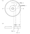
ここで、アライメントマークについて説明する。1つの面に記録面を持つ光記録媒体基板や光記録媒体シートを複数積層する場合について説明する。1つの記録面を持つ光記録媒体基板や光記録媒体シートをそれぞれ、”層”と称する。 Here, the alignment mark will be described. A case where a plurality of optical recording medium substrates and optical recording medium sheets having a recording surface on one surface are stacked will be described. Each of the optical recording medium substrate and the optical recording medium sheet having one recording surface is referred to as a “layer”.
図4は本発明によるアライメントマークの一例を説明する概念図である。 FIG. 4 is a conceptual diagram illustrating an example of an alignment mark according to the present invention.
例えば、第1層41、第2層42、第3層43・・・に、それぞれ半径がr1、r2、r3・・・のように異なるアライメントマークAM1、AM2、AM3が形成される。さらに、少なくとも1つの基準となる第B層40には、例えば前記、各アライメントマークに対応する基準アライメントマークAMB1、AMB2、AMB3が形成されている。この基準アライメントマークは、どの層に形成しても良い。 For example, alignment marks AM1, AM2, and AM3 having different radii such as r1, r2, r3,... Are formed on the first layer 41, the second layer 42, the third layer 43,. Further, for example, the reference alignment marks AMB1, AMB2, and AMB3 corresponding to the alignment marks are formed on the B-layer 40 serving as at least one reference. This reference alignment mark may be formed in any layer.
アライメントマークはデータ記録領域以外に形成すればよく、最終的にディスクに転写されるような半径に形成しても良いし、ディスクに転写されない半径(例えば、ディスクの中心穴より小さい半径や、ディスクの外径より大きい半径)に形成しても良い。また、連続的な線状でなく、断続的な形状でも良い。 The alignment mark may be formed outside the data recording area, and may be formed at a radius that is finally transferred to the disk, or a radius that is not transferred to the disk (for example, a radius smaller than the center hole of the disk, or the disk May be formed with a radius larger than the outer diameter. Further, it may be an intermittent shape instead of a continuous linear shape.
図5は本発明による光記録媒体シートの作成方法の一例を示す模式図である。
光記録媒体シートを作製するためのスタンパは、上述した光記録媒体基板を作製するためのスタンパと同様な方法で作製することができる。
FIG. 5 is a schematic view showing an example of a method for producing an optical recording medium sheet according to the present invention.
The stamper for producing the optical recording medium sheet can be produced by the same method as the stamper for producing the optical recording medium substrate described above.
図5(a)に示すように、例えば、熱硬化性樹脂や紫外線硬化樹脂等の凹凸形状を転写することが可能な材料や、または圧力によって凹凸形状を転写することが可能な材料に、スタンパ51を押し当てて、表面に凹凸形状を転写することで、光記録媒体シート53を形成する。次に、図5(c)に示すように、凹凸形状が形成された面に例えばスパッタリング法などによって記録層または反射層54を形成する。必要に応じて、誘電体層、記録層、半透過性の反射層、反射層を形成する。 As shown in FIG. 5A, for example, a stamper is applied to a material capable of transferring an uneven shape, such as a thermosetting resin or an ultraviolet curable resin, or a material capable of transferring an uneven shape by pressure. The optical recording medium sheet 53 is formed by pressing 51 to transfer the uneven shape onto the surface. Next, as shown in FIG. 5C, a recording layer or a reflective layer 54 is formed on the surface on which the concavo-convex shape is formed, for example, by sputtering. If necessary, a dielectric layer, a recording layer, a semi-transmissive reflective layer, and a reflective layer are formed.
ここで、多層に積層する際に、前記記録層または反射層によってアライメントマークが検出できなくなってしまう場合は、アライメント領域に前記記録層または反射層を形成しない構成にすればよい。また、前記記録層または反射層の形成によりアライメントマークの識別がより良好になる場合は、アライメント領域に前記記録層または反射層を形成する構成にしても良い。 Here, in the case where the recording layer or the reflective layer makes it impossible to detect the alignment mark when the layers are laminated, the recording layer or the reflective layer may be configured not to be formed in the alignment region. Further, in the case where the alignment mark is identified better by forming the recording layer or the reflective layer, the recording layer or the reflective layer may be formed in the alignment region.
上記本発明による光記録媒体には、白色光で容易に識別が可能な反射率が得られる深さでピットまたは連続溝からなるアライメント凹凸が形成されているため、シート状に形成された光記録媒体シートを複数積層させる際に、顕微鏡を用いて偏芯量の少ない位置合わせが可能となる。 In the optical recording medium according to the present invention, since the alignment irregularities made of pits or continuous grooves are formed at a depth at which a reflectance that can be easily identified with white light is obtained, the optical recording formed in a sheet shape. When a plurality of media sheets are stacked, alignment with a small amount of eccentricity can be performed using a microscope.
(実施例1)
以下、本発明に従う光記録媒体の詳細な実施例について説明するが、この構成に限定される物ではない。
(Example 1)
Hereinafter, although the detailed Example of the optical recording medium according to this invention is described, it is not a thing limited to this structure.
本実施例では、少なくとも片方の面に記録面を持つ基板および、シートを積層する構成を例に、詳しくは、第0層としては基板を、第1層、第2層、第3層としてはシートを積層する4層構成の光記録媒体を例に説明する。 In this embodiment, a substrate having a recording surface on at least one surface and a structure in which sheets are stacked are taken as an example. Specifically, the substrate is the 0th layer, the first layer, the second layer, and the third layer are An optical recording medium having a four-layer structure in which sheets are laminated will be described as an example.
レジストとして化学量論組成から微量に酸素が欠損した組成のネガ型の酸化タングステンWO1-xを例に説明する。化学量論組成から酸素が微量に欠損した酸化タングステンWO1-xは、露光用の光を照射することで層の状態が変わり、体積が増え、露光部が凸となる。さらに、体積変化量は、露光用の光の移動速度及び、強度によって調整することができる。 A negative type tungsten oxide WO 1-x having a composition in which oxygen is deficient in a trace amount from a stoichiometric composition will be described as an example of the resist. Tungsten oxide WO 1-x in which a small amount of oxygen is lost from the stoichiometric composition changes the state of the layer by irradiating light for exposure, the volume increases, and the exposed portion becomes convex. Furthermore, the volume change amount can be adjusted by the moving speed and intensity of the exposure light.
化学量論組成から酸素が微量に欠損した酸化タングステンWO1-xは、スパッタ法を用いて形成することができる。ターゲットにWを用い、酸素雰囲気中でスパッタする方法と、化学量論組成から酸素が微量に欠損した酸化タングステンWO1-xをターゲットとして用い、不活性ガス(窒素を除く)雰囲気でスパッタしても良い。 Tungsten oxide WO 1-x in which a small amount of oxygen is lost from the stoichiometric composition can be formed by sputtering. Sputtering in an atmosphere of inert gas (excluding nitrogen) using tungsten as a target and sputtering in an oxygen atmosphere and tungsten oxide WO 1-x in which a small amount of oxygen is lost from the stoichiometric composition as a target Also good.
ネガ型の酸化タングステンWO1-xは、スパッタリングを行った状態ではアルカリ可溶性である。露光によって層の状態を変えることでアルカリ不溶性にすることができる。レジスト設計としては、露光用の光に対する光学特性、露光用の光に対する体積変化量、現像用の溶剤に対するエッチング特性、形成される溝形状等を考慮して、最適な組成と層厚を選ぶことができる。本実施例では、層厚100nmの酸化タングステンを、形成した。 The negative type tungsten oxide WO 1-x is alkali-soluble in the sputtered state. Alkali insolubility can be achieved by changing the state of the layer by exposure. For resist design, select the optimal composition and layer thickness in consideration of optical characteristics for exposure light, volume variation with respect to exposure light, etching characteristics with respect to solvent for development, groove shape to be formed, etc. Can do. In this example, tungsten oxide having a layer thickness of 100 nm was formed.
アライメントマーク領域として記録領域の内側、アライメントマーク形状として同心円形状を用いた場合を例に説明する。 The case where the inside of the recording area is used as the alignment mark area and the concentric circle shape is used as the alignment mark shape will be described as an example.
図6は実施例1による光記録媒体製造用マスタリング原盤の作成方法を説明する模式図である。 FIG. 6 is a schematic diagram for explaining a method for producing a mastering master for producing an optical recording medium according to the first embodiment.
図6(a)に示すように、石英原盤61上に、化学量論組成から微量に酸素が欠損した酸化タングステンを形成し、レジスト原盤とした。化学量論組成から微量に酸素が欠損した酸化タングステンは、Wを含んだターゲットを、ArガスとO2ガスの雰囲気中でスパッタリングすることで形成した。 As shown in FIG. 6 (a), tungsten oxide in which a small amount of oxygen was lost from the stoichiometric composition was formed on a quartz master 61 to obtain a resist master. Tungsten oxide deficient in oxygen from a stoichiometric composition was formed by sputtering a target containing W in an atmosphere of Ar gas and O 2 gas.
酸化タングステンの酸素の量は、ArガスとO2ガスの比率を変えることで組成を調整することができる。層厚はスパッタリング時間で調整することができる。実施例1では、層厚は100nmとし、露光光である351nmの波長に対して吸収率が30%である組成とした。 The amount of oxygen in tungsten oxide can be adjusted by changing the ratio of Ar gas to O 2 gas. The layer thickness can be adjusted by the sputtering time. In Example 1, the layer thickness was 100 nm, and the composition had an absorptivity of 30% with respect to the wavelength of 351 nm as exposure light.
尚、前記金属の酸化物からなるレジストは組成によって、351nmの波長の吸収率が30%程度の膜が形成できるので、レジスト原盤に合成石英製の基板のような紫外領域の透過率の高い基板を用いることで、樹脂を用いた透明スタンパに変えて透明スタンパとして使用することができる。この場合、樹脂製の透明スタンパのように使い捨てにする必要がないので生産効率を向上することができる。 The resist made of the metal oxide can form a film having an absorptance of about 30% at a wavelength of 351 nm depending on the composition. Therefore, a substrate having a high ultraviolet region transmittance such as a synthetic quartz substrate is used as a resist master. Can be used as a transparent stamper instead of a transparent stamper using a resin. In this case, since it is not necessary to use a disposable stamper made of resin, production efficiency can be improved.
次に、露光を行う。図6(b)に示すように、露光源から露光用の光63をレジストに集光させ、レジスト原盤を回転させながら、露光源をディスクの半径方向64に、移動させることで、レジスト上に凸状の螺旋状の露光パターンを形成した。 Next, exposure is performed. As shown in FIG. 6B, the exposure light 63 is condensed on the resist from the exposure source, and the exposure source is moved in the radial direction 64 of the disk while rotating the resist master, so that the resist is moved onto the resist. A convex spiral exposure pattern was formed.
本実施例では、露光用の光63の波長は351nmとした。データ記録領域の露光条件は、線速0.7m/s、パワー1.4mWとし、アライメントマーク領域の露光条件は、線速2m/s、パワー1.4mWとした。トラックピッチTPはどちらも320nmとした。 In this embodiment, the wavelength of the exposure light 63 is 351 nm. The exposure conditions for the data recording area were a linear velocity of 0.7 m / s and a power of 1.4 mW, and the exposure conditions for the alignment mark area were a linear speed of 2 m / s and a power of 1.4 mW. Both track pitches TP were 320 nm.
この結果、図6(c)に示すように、データ記録領域には、幅150nm、高さd’(d)=5nmの凸状の露光パターンが形成され、アライメント領域には、幅120nm、高さd’(am)=30nmの凸状の露光パターンが形成された。ここで、13レジストの体積変化について簡単に考察する。露光時の線速が異なることでレジストの加熱時間や加熱される温度勾配、冷却状況が変わる。その結果、レジストの結晶状態が変わり、体積が変わると考えられる。 As a result, as shown in FIG. 6C, a convex exposure pattern having a width of 150 nm and a height d ′ (d) = 5 nm is formed in the data recording area, and the alignment area has a width of 120 nm and a high height. A convex exposure pattern of d ′ (am) = 30 nm was formed. Here, the volume change of 13 resists will be briefly considered. The resist heating time, the temperature gradient to be heated, and the cooling state change depending on the linear velocity at the time of exposure. As a result, it is considered that the crystal state of the resist changes and the volume changes.
次に、現像を行う。図6(d)に示すように、アルカリの現像液(TMAH(Tetramethyl ammonium hydroxide:水酸化テトラメチルアンモニウム)0.5%)を用いて未露光部のレジストを除去し、データ記録領域の溝深さがd(d)=20nm、アライメントマーク領域の溝深さがd(am)=35nmになるように現像を行った。 Next, development is performed. As shown in FIG. 6D, unexposed resist is removed using an alkali developer (TMAH (tetramethylammonium hydroxide: 0.5%)), and the groove depth of the data recording area is removed. Is developed so that the length of the groove in the alignment mark region is d (am) = 35 nm.
アルカリの現像液としては、KOH、NaOH等を用いることもできる。 As the alkaline developer, KOH, NaOH, or the like can be used.
次に、アライメントマークの説明をする。実施例1では、図7(a)に示すようにアライメントマーク領域を、データ記録領域よりも内周側に設けた。形状としては、図8に示すようなアライメントマークを用いた。第1層、第2層、第3層には、それぞれアライメントマークAM1、AM2、AM3を形成した。第0層には、アライメントマークAM1、AM2、AM3に対応するアライメントマークAM01、AM02、AM03を形成した。 Next, the alignment mark will be described. In Example 1, as shown in FIG. 7A, the alignment mark area is provided on the inner peripheral side of the data recording area. As the shape, an alignment mark as shown in FIG. 8 was used. Alignment marks AM1, AM2, and AM3 were formed on the first layer, the second layer, and the third layer, respectively. On the 0th layer, alignment marks AM01, AM02, AM03 corresponding to the alignment marks AM1, AM2, AM3 were formed.
アライメントマークは、全体像としては同心円だが、図8(b)の拡大図に示すように、螺旋状の複数のトラックからなる。また、アライメントマークAM1、AM2、AM3はそれぞれが重ならないように半径が異なっている。対応するそれぞれのアライメントマーク同士AM1とAM01、AM2とAM02、AM3とAM03も重ならないように半径が異なっている。 The alignment mark is a concentric circle as a whole image, but includes a plurality of spiral tracks as shown in the enlarged view of FIG. The alignment marks AM1, AM2, and AM3 have different radii so that they do not overlap each other. The corresponding alignment marks have different radii so that AM1 and AM01, AM2 and AM02, and AM3 and AM03 do not overlap.
本実施例では、アライメントマークAM1、AM2及びAM3を、それぞれ、半径20.75mm〜20.85mm、20.45mm〜20.55mm、20.15mm〜20.25mmの位置に形成した。 In this embodiment, the alignment marks AM1, AM2, and AM3 were formed at positions having radii of 20.75 mm to 20.85 mm, 20.45 mm to 20.55 mm, and 20.15 mm to 20.25 mm, respectively.
幅0.1mmのアライメント領域中に、ピッチ0.32μmで形成された溝の集合体を円と考えることができる。アライメントマークの幅は、観測に用いる顕微鏡で観察可能であればよく、好ましくは5μm以上を選ぶことができる。 An aggregate of grooves formed at a pitch of 0.32 μm in an alignment region having a width of 0.1 mm can be considered as a circle. The width of the alignment mark only needs to be observable with a microscope used for observation, and preferably 5 μm or more can be selected.
対応するアライメントマークAM01、AM02及びAM03を、20.6mm〜20.7mm半径、20.3mm〜20.4mm、20mm〜20.1mmに形成した。 Corresponding alignment marks AM01, AM02 and AM03 were formed to have a radius of 20.6 mm to 20.7 mm, 20.3 mm to 20.4 mm, and 20 mm to 20.1 mm.
実施例1のアライメントマークは同心円状(スパイラル状)であり、データ信号と連続的に形成されるので、偏芯量が殆ど無い。 The alignment mark of Example 1 is concentric (spiral) and formed continuously with the data signal, so there is almost no eccentricity.
上述の説明は、螺旋を用いて説明したが、螺旋の変わりに、同心円を形成しても同じ効果を得ることができる。 Although the above description has been made using a spiral, the same effect can be obtained by forming concentric circles instead of the spiral.
上記それぞれのアライメントマークを形成した、第0層用マスタリング原盤、第1層用マスタリング原盤、第2層用マスタリング原盤、第3層用マスタリング原盤をそれぞれ作成した。 A mastering master for the 0th layer, a mastering master for the first layer, a mastering master for the second layer, and a mastering master for the third layer, each having the alignment marks described above, were prepared.
次に図7(b)に示すように、それぞれのマスタリング原盤にNi電鋳を行い、第0層形成用スタンパ、第1層形成用スタンパ、第2層形成用スタンパ、第3層形成用スタンパを作製した。 Next, as shown in FIG. 7B, Ni electroforming is performed on each mastering master, and the 0th layer forming stamper, the 1st layer forming stamper, the 2nd layer forming stamper, and the 3rd layer forming stamper. Was made.
次に、図9(a)に示すように、第0層形成用スタンパ94の中央部に中心穴91を打ち抜いて形成した。中心穴の形成は、打ち抜き機を用いて、例えばアライメントマークAM03を顕微鏡で観察し、偏芯合わせの位置調整を行うことで、偏芯量の少ない中心穴の形成を行う事ができた。本発明のアライメントマークは溝深さが35nmの凹凸が形成されているために、顕微鏡でのアライメントマークの識別が可能となる。 Next, as shown in FIG. 9A, a center hole 91 was formed by punching in the central portion of the stamper 94 for forming the 0th layer. The center hole was formed using a punching machine, for example, by observing the alignment mark AM03 with a microscope and adjusting the position of the eccentric alignment, thereby forming the center hole with a small amount of eccentricity. Since the alignment mark of the present invention is provided with irregularities having a groove depth of 35 nm, the alignment mark can be identified with a microscope.
次に、図9(b)に示すように、第0層の光記録媒体基板を形成した。実施例1では、第0層形成用スタンパを射出成型用金型にセットし、厚さ、1.1mmのポリカーボネート樹脂を用いて、第0層の光記録媒体基板を成型した。 Next, as shown in FIG. 9B, a zeroth-layer optical recording medium substrate was formed. In Example 1, the 0th layer forming stamper was set in an injection mold, and the 0th layer optical recording medium substrate was molded using a polycarbonate resin having a thickness of 1.1 mm.
これにより、基板の表面にデータ記録領域及びアライメントマーク領域の凹凸、及び偏芯量のほとんど無い中心穴が形成された第0層の光記録媒体基板93が形成された。 As a result, the 0th layer optical recording medium substrate 93 was formed on the surface of the substrate in which the concave and convex portions of the data recording area and the alignment mark area and the central hole having almost no eccentricity were formed.
次に、第1層形成用スタンパ、第2層形成用スタンパ、第3層形成用スタンパを用いて、第1層、第2層、第3層の光記録媒体シートを作製した。 Next, first layer, second layer, and third layer optical recording medium sheets were prepared using a first layer forming stamper, a second layer forming stamper, and a third layer forming stamper.
図10は本発明による光記録媒体の作成方法の一例を示す模式図である。シートの厚さとしては、12μm、13μm、14μmのシート厚さを用いた。各層のシートの厚さを変えることで、接着剤の厚さを変えることなく、層間距離を変えることができ、各層の信号干渉を抑えることが出来た。シートの材料として、熱可塑性樹脂が使える。本実施例では、ポリカーボネート樹脂のシート基材を用いた。 FIG. 10 is a schematic diagram showing an example of a method for producing an optical recording medium according to the present invention. As the sheet thickness, sheet thicknesses of 12 μm, 13 μm, and 14 μm were used. By changing the thickness of the sheet of each layer, it was possible to change the interlayer distance without changing the thickness of the adhesive, and to suppress the signal interference of each layer. A thermoplastic resin can be used as a material for the sheet. In this embodiment, a polycarbonate resin sheet base material was used.
図10(a)に示すように、スタンパ101をヒータ102でポリカーボネート樹脂の熱変形温度以上に加熱しながら、シート103に押し付けることで、スタンパ上の凹凸をシート表面に転写した。次に、スタンパを冷却した後に、スタンパとシートを剥離した。これにより、シート103の表面にデータ記録領域及びアライメントマーク領域の凹凸が形成された各層の光記録媒体シート104が形成された。ここで、上記ポリカーボネート樹脂の熱変形温度は120℃であった。シートの材料及び基板の材料としては、記録、再生、消去を行う際に光学的に支障のない材料であれば良く、特に限定される物ではない。 As shown in FIG. 10A, the stamper 101 was pressed against the sheet 103 while being heated to a temperature higher than the heat distortion temperature of the polycarbonate resin by the heater 102, thereby transferring the irregularities on the stamper to the sheet surface. Next, after the stamper was cooled, the stamper and the sheet were peeled off. Thereby, the optical recording medium sheet 104 of each layer in which the unevenness of the data recording area and the alignment mark area was formed on the surface of the sheet 103 was formed. Here, the heat distortion temperature of the polycarbonate resin was 120 ° C. The material of the sheet and the material of the substrate are not particularly limited as long as they are materials that do not optically interfere with recording, reproduction, and erasing.
以上のように作製された各光記録媒体に、記録層を形成する。記録層の構成としては、例えば、誘電体層、記録層、誘電体層、反射層もしくは反射層を形成する。実施例1においては、図11に示すように、データ記録領域以外の部分(基板の内周囲のアライメント部分及び基板の外周囲)をマスクによりカバーすることで、アライメント領域には、記録層が形成されない構成とした。 A recording layer is formed on each optical recording medium manufactured as described above. As the configuration of the recording layer, for example, a dielectric layer, a recording layer, a dielectric layer, a reflective layer, or a reflective layer is formed. In the first embodiment, as shown in FIG. 11, a recording layer is formed in the alignment region by covering portions other than the data recording region (the alignment portion on the inner periphery of the substrate and the outer periphery of the substrate) with a mask. The configuration was not.
光記録膜材料としては、Te、In、Ga、Sb、Se、Pb、Ag、Au、As、Co、Ni、Mo、W、Pd、Ti、Bi、Zn、Si等の材料の少なくとも1種類以上からなる合金等などが幅広く一般的に知られている。これらは、すでに多くの材料が公知の技術として存在する。 As an optical recording film material, at least one kind of materials such as Te, In, Ga, Sb, Se, Pb, Ag, Au, As, Co, Ni, Mo, W, Pd, Ti, Bi, Zn, and Si are used. Alloys made of and the like are widely known. Many of these materials already exist as known techniques.
その他にも光磁気記録材料としてTb、Fe、Co、Cr、Gd、Dy、Nd、Sm、Ce、Ho等の材料の少なくとも1種類以上からなる合金、希土類-遷移金属合金が多く用いられており、これらもすでに多くの材料が公知の技術として存在する。 In addition, alloys made of at least one of Tb, Fe, Co, Cr, Gd, Dy, Nd, Sm, Ce, Ho, and other rare earth-transition metal alloys are often used as magneto-optical recording materials. Many of these materials already exist as known techniques.
反射膜材料としてもAlやAl合金、又はSiやSiN及びAgやAg合金などが用いられており、すでに多くの材料が公知の技術として存在する。 Al, Al alloy, Si, SiN, Ag, Ag alloy, and the like are also used as the reflective film material, and many materials already exist as known techniques.
さらに、シアニン系やフタロシアニン系やアゾ系などの有機色素系の材料を記録層として用いることができる。 Furthermore, organic dye-based materials such as cyanine-based, phthalocyanine-based, and azo-based materials can be used as the recording layer.
上記記録層又は反射層の膜厚は、任意に設定できるが、光入射面側から各記録層及び反射層で光の減衰が生じるため用いる光の波長における透過率を入射面側に近い層程高めることが望ましい。また、各記録層及び反射層の組成や膜厚を調整して各層の記録・再生・消去に支障のない構成にすることが好ましい。
成膜方法についてはスパッタリング方、蒸着法、CVD法、ディッピング塗布、スピンコート塗布などが考えられ、各々の生産工程、生産装置及び生産する記録媒体に最適な方式であれば良く特に限定されるものではない。
The film thickness of the recording layer or the reflective layer can be arbitrarily set, but since the light attenuation occurs in each recording layer and the reflective layer from the light incident surface side, the transmittance at the wavelength of the light used is closer to the incident surface side. It is desirable to increase. Further, it is preferable to adjust the composition and film thickness of each recording layer and the reflective layer so as not to hinder the recording / reproducing / erasing of each layer.
As the film forming method, a sputtering method, a vapor deposition method, a CVD method, a dipping coating, a spin coating coating, and the like can be considered, and any method that is optimal for each production process, production apparatus, and recording medium to be produced is particularly limited. is not.
各シート基材及び基板ごとに、組成や膜厚及び成膜条件などを最適化することで、任意の透過率と反射率の記録層及び反射層を形成することができる。 By optimizing the composition, film thickness, film forming conditions, and the like for each sheet base material and substrate, a recording layer and a reflective layer having arbitrary transmittance and reflectance can be formed.
本発明では必要とされる光記録媒体に適した記録層材料を用いることで、特に限定されるものではない。 In the present invention, there is no particular limitation by using a recording layer material suitable for the required optical recording medium.
次に、各層の光記録媒体を積層した。 Next, an optical recording medium of each layer was laminated.
図12は、実施例1の重ね合わせ工程を説明するための模式図である。 FIG. 12 is a schematic diagram for explaining the superposition process of the first embodiment.
第0層120は、図11で説明した、光記録媒体基板と記録層からなり、第1層121、第2層122、第3層123は光記録媒体シートおよび記録層からなる。 The 0th layer 120 includes the optical recording medium substrate and the recording layer described with reference to FIG. 11, and the first layer 121, the second layer 122, and the third layer 123 include the optical recording medium sheet and the recording layer.
実施例1では、各層の接着には、透明な感圧性接着シートを用いて圧着した。感圧性接着シートは、記録・再生に用いるレーザ光の波長に対して透過率が高い材料であればよい。 In Example 1, each layer was bonded using a transparent pressure-sensitive adhesive sheet. The pressure-sensitive adhesive sheet may be a material having a high transmittance with respect to the wavelength of the laser beam used for recording / reproduction.
まず、第0層120、第1層121、第2層122、第3層123の間に感圧性接着シート(図示せず)を挟み、各層をある程度密着した状態で重ねあわせる。 First, a pressure-sensitive adhesive sheet (not shown) is sandwiched between the 0th layer 120, the first layer 121, the second layer 122, and the third layer 123, and the layers are overlapped with each other being in close contact with each other.
紙面に直交する方向Bの位置合わせについては位置合わせ駆動装置124によって、各層それぞれにおいて、精密に位置合わせを行った。矢印A方向の位置あわせは各層を保持しているローラ126によって精密な位置合わせを行った。
Regarding the alignment in the direction B perpendicular to the paper surface, the
ここでアライメントマークによる位置合わせの説明をする。図8(c)に示すように、例えば、円周上の4個所A、B、C、Dの位置を、4箇所でのAM01とAM1との距離が同じになるように位置合わせをする。同様にAM02とAM2との距離、及び、AM03とAM3との距離が同じになるように調整した。 Here, the alignment by the alignment mark will be described. As shown in FIG. 8C, for example, the positions of four locations A, B, C, and D on the circumference are aligned so that the distances between AM01 and AM1 at the four locations are the same. Similarly, the distance between AM02 and AM2 and the distance between AM03 and AM3 were adjusted to be the same.
図8では、顕微鏡を用いて位置合わせを行った。 In FIG. 8, alignment was performed using a microscope.
距離の測定は、顕微鏡の40倍の対物レンズと10倍の接眼レンズに形成された10mmを100等分したスケールメモリを用いて測定を行った。40倍の対物レンズと10倍の接眼レンズに形成された10mmを100等分したスケールメモリで測定する場合、1目盛りの寸法が、2.50μmになるので十分に位置合わせを行うことができる。 The distance was measured using a scale memory in which 10 mm formed on a 40 × objective lens and a 10 × eyepiece of the microscope were divided into 100 equal parts. When measuring with a scale memory obtained by equally dividing 10 mm formed on a 40 × objective lens and a 10 × eyepiece lens into 100 equal parts, since the size of one scale is 2.50 μm, sufficient alignment can be performed.
本実施例のアライメントマークは溝深さ35nmの凹凸が形成されているために、白色光で識別が容易であるので、複数の層を透過してアライメントマークを認識し、多層の位置合わせを、まとめて行う事ができる。さらに、各層のアライメントマークを、基準となる層に設けた基準アライメントマークに対して位置合わせするので、偏芯のズレが累積されない。また、アライメントマークを、データ信号領域以外に形成するので、データ領域の面積を減らさずにすむ。 Since the alignment mark of the present embodiment is formed with irregularities with a groove depth of 35 nm, it is easy to identify with white light. Therefore, the alignment mark is recognized through the plurality of layers, and the alignment of the multilayer is performed. Can be done together. Furthermore, since the alignment marks of the respective layers are aligned with respect to the reference alignment marks provided on the reference layer, deviations in eccentricity are not accumulated. Further, since the alignment mark is formed outside the data signal region, it is not necessary to reduce the area of the data region.
アライメントパターンの深さは35nm以上であれば、白色光を用いて問題なく位置合わせを行うことができた。 If the depth of the alignment pattern was 35 nm or more, alignment could be performed without any problem using white light.
このようにして積層した後に、シート状に形成した第1層121、第2層122、第3層123を打ち抜き装置(図示しない)によって圧着すると同時に、打ち抜く。この時、内径を第0層の光記録媒体基板よりも大きな半径に一括で打ち抜き、外径を第0層の光記録媒体よりも小さな半径に一括で打ち抜いた。但し、第0層の光記録媒体基板は打ち抜かないように打ち抜き機を調整した。図12(b)に示すように、4層構成の光記録媒体形状に形成した。更に最上層に凹凸パターンを有しない75μmの保護シート127を張り合わせて、4層構成の光記録媒体を完成させた。 After laminating in this manner, the first layer 121, the second layer 122, and the third layer 123 formed in a sheet shape are pressure-bonded by a punching device (not shown) and simultaneously punched. At this time, the inner diameter was collectively punched to a radius larger than that of the 0th layer optical recording medium substrate, and the outer diameter was collectively punched to a radius smaller than that of the 0th layer optical recording medium. However, the punching machine was adjusted so as not to punch the 0th layer optical recording medium substrate. As shown in FIG. 12B, a four-layer optical recording medium was formed. Further, a 75 μm protective sheet 127 having no uneven pattern was laminated on the uppermost layer to complete a four-layer optical recording medium.
完成した4層構成の光記録媒体の保護コート面側から波長405nmのレーザ光を用いて再生評価を行ったところ、各層とも偏芯量が少なく、かつ良好な再生が出来た。 When reproduction evaluation was performed using a laser beam having a wavelength of 405 nm from the protective coating surface side of the completed optical recording medium having a four-layer structure, each layer had a small amount of eccentricity and good reproduction was achieved.
本実施例によれば、データ信号に対して偏芯量がほとんど無い中心穴を持つ第0層上に、他の層を偏芯量がほとんど無い状態で積層できるので、中心穴の中心に対する各層の偏芯を20μmP−P以下に調整することが出来た。 According to the present embodiment, other layers can be stacked on the 0th layer having a center hole having almost no eccentricity with respect to the data signal in a state where there is almost no eccentricity. Can be adjusted to 20 μm P-P or less.
(実施例2)
実施例2では実施例1で作製した、第0層の光記録媒体基板93に、記録層を形成し、最上層に凹凸パターンを有しない100μmの保護シートを張り合わせて光記録媒体を完成させた。完成した光記録媒体の保護コート面側から波長405nmのレーザ光を用いて再生評価を行ったところ、各層とも偏芯量が少なく、かつ良好な再生が出来た。
(Example 2)
In Example 2, a recording layer was formed on the optical recording medium substrate 93 of the 0th layer produced in Example 1, and a 100 μm protective sheet having no concavo-convex pattern was laminated on the uppermost layer to complete the optical recording medium. . When reproduction was evaluated using a laser beam having a wavelength of 405 nm from the protective coating surface side of the completed optical recording medium, each layer had a small amount of eccentricity and good reproduction was possible.
(実施例3)
実例施3では、感光してアルカリ不溶性からアルカリ可溶性に変化する、フォトンモードのレジストを例に説明する。
(Example 3)
In
13フォトンモードのレジストは、露光用の光照射量によって、レジストが感光する量、すなわち変化する深さが変わるので、露光用の光照射条件と現像条件によって凹凸の深さを変えることができる。 In the 13-photon mode resist, the amount of exposure of the resist, that is, the changing depth varies depending on the exposure light irradiation amount. Therefore, the depth of the unevenness can be changed depending on the exposure light irradiation condition and the development condition.
図13(a)に示すように、石英原盤131上に、ノボラック系i線レジストを100nmの厚さに形成した。 As shown in FIG. 13A, a novolac i-line resist was formed on a quartz master 131 to a thickness of 100 nm.
次に、露光を行う。図13(b)に示すように、露光用の光133をレジストに集光させ、レジスト原盤を回転させながら、露光用の光(露光光源)をディスクの半径方向134に移動させ、レジスト原盤を、レジスト上に螺旋状の露光パターンを形成した。データ記録領域の露光条件は、線速2.0m/s、パワー0.2mWとし、アライメントマーク領域の露光条件は、線速2m/s、パワー0.5mWとした。データ記録領域のトラックピッチTPは320nm、アライメントマーク領域のトラックピッチTTPは1μmとした。 Next, exposure is performed. As shown in FIG. 13B, the exposure light 133 is condensed on the resist, the exposure light (exposure light source) is moved in the radial direction 134 of the disk while rotating the resist master, and the resist master is moved. A spiral exposure pattern was formed on the resist. The exposure conditions for the data recording area were a linear speed of 2.0 m / s and a power of 0.2 mW, and the exposure conditions for the alignment mark area were a linear speed of 2 m / s and a power of 0.5 mW. The track pitch TP in the data recording area was 320 nm, and the track pitch TTP in the alignment mark area was 1 μm.
次に、現像を行う。図13(d)に示すように、アルカリ現像液TMAH0.5%を用いて感光によって変化した部分のレジストを除去し、データ記録領域の溝深さがd(d)=20nm、アライメントマーク領域の溝深さがd(am)=100nmになるように現像を行った。 Next, development is performed. As shown in FIG. 13D, the portion of the resist changed by exposure is removed using an alkali developer TMAH 0.5%, the groove depth of the data recording area is d (d) = 20 nm, and the alignment mark area Development was performed so that the groove depth was d (am) = 100 nm.
ここで、溝深さが深く、かつトラックピッチも広いため、実施例3のアライメントマークは実施例1のアライメントマークと比べて、顕微鏡での識別がより良好であった。 Here, since the groove depth was deep and the track pitch was wide, the alignment mark of Example 3 was better identified with the microscope than the alignment mark of Example 1.
上記以外は実施例1と同様の工程で光記録媒体を作製した。実施例1と同様に再生評価を行ったところ、中心穴の中心に対する各層の偏芯を10μmP−P以下に調整することが出来かつ良好な再生が出来た。 Except for the above, an optical recording medium was produced in the same steps as in Example 1. When reproduction evaluation was performed in the same manner as in Example 1, the eccentricity of each layer with respect to the center of the center hole could be adjusted to 10 μm P-P or less, and good reproduction was possible.
(実施例4)
実施例4ではアライメントマークのトラックピッチを1μmとした以外は実施例1と同様の工程で光記録媒体を作製した。ここで、実施例3のアライメントマークは実施例1のアライメントマークと比べて、顕微鏡での識別がより良好であった。実施例1と同様に再生評価を行ったところ、中心穴の中心に対する各層の偏芯を15μmP−P以下に調整することが出来、かつ良好な再生が出来た。
Example 4
In Example 4, an optical recording medium was manufactured in the same process as in Example 1 except that the track pitch of the alignment mark was 1 μm. Here, the alignment mark of Example 3 was better identified with a microscope than the alignment mark of Example 1. When reproduction evaluation was performed in the same manner as in Example 1, the eccentricity of each layer with respect to the center of the center hole could be adjusted to 15 μm P-P or less, and good reproduction was possible.
11 データ記録領域
12 アライメントマーク領域
13 凹凸
14 凹凸
21 ガラス原盤21
22 レジスト22
23 露光用の光23
25 マスタリング原盤
31 マスタリング原盤
32 スタンパ
33 中心穴
40 B層
41 第1層
42 第2層
43 第3層
51 スタンパ
53 光記録媒体シート
54 記録膜
61 石英原盤
62 レジスト
63 露光用の光
91 中心穴
92 中心穴
93 第0層光記録媒体基板
94 第0層形成用スタンパ
101 スタンパ
102 ヒータ
103 シート
104 光記録媒体シート
111 記録膜
120 第0層
121 第1層
122 第2層
123 第3層
124 位置合わせ駆動装置
125 光学顕微鏡
126 ローラ
127 保護シート
131 石英原盤
132 レジスト
135 マスタリング原盤
141 記録媒体シート
142 多層光記録媒体
143 打ち抜き機
144 多層光記録媒体
145 支持基板
11 Data recording area 12 Alignment mark area 13 Concavity and convexity 14 Concavity and convexity 21 Glass master 21
22 resist 22
23 Light 23 for exposure
25 Mastering master 31 Mastering master 32 Stamper 33 Center hole 40 B layer 41 First layer 42 Second layer 43 Third layer 51 Stamper 53 Optical recording medium sheet 54 Recording film 61 Quartz master disk 62 Resist 63 Light for exposure 91 Center hole 92 Center hole 93 0th layer optical recording medium substrate 94 0th layer forming stamper 101 stamper 102 heater 103 sheet 104 optical recording medium sheet 111 recording film 120 0th layer 121 1st layer 122 2nd layer 123
Claims (16)
前記光記録媒体は、データ記録領域と少なくとも前記データ記録領域の内周囲あるいは外周囲のいずれか一方に前記2以上の記録層間の位置を合わせるためのアライメント領域を有し、
前記データ領域に形成された信号パターンの深さよりも前記アライメント領域に形成されたアライメントパターンの深さが深いことを特徴とする光記録媒体。 An optical recording medium having two or more recording layers,
The optical recording medium has an alignment area for aligning the position of the two or more recording layers with either a data recording area and at least one of an inner periphery and an outer periphery of the data recording area,
An optical recording medium, wherein an alignment pattern formed in the alignment region is deeper than a signal pattern formed in the data region.
前記光記録媒体の第1の情報記録層が形成された第1の記録領域の内周囲あるいは外周囲のいずれか一方に第1のアライメント領域を有し、
前記シートの第2の情報記録層が形成された第2の記録領域の内周囲あるいは外周囲のいずれか一方に第2のアライメント領域を有することを特徴とする請求項1に記載の光記録媒体。 The optical recording medium is a laminate of a substrate or sheet on which a first information recording layer is formed and a sheet on which at least one surface has a second information recording layer formed,
A first alignment region on either the inner periphery or the outer periphery of the first recording region on which the first information recording layer of the optical recording medium is formed;
2. The optical recording medium according to claim 1, further comprising a second alignment area on either the inner periphery or the outer periphery of the second recording area on which the second information recording layer of the sheet is formed. .
前記スタンパの前記データ領域に形成された信号パターンの深さよりも前記アライメント領域に形成されたアライメントパターンの深さが深いことを特徴とする光記録媒体製造用スタンパ。 The alignment in which the alignment region is provided with a data recording region in which a signal pattern is formed and a sheet and a substrate having an alignment region in which an alignment pattern is formed at least either on the inner periphery or the outer periphery of the data recording region An optical recording medium manufacturing stamper for manufacturing the substrate or the sheet of optical recording media laminated using a pattern,
A stamper for manufacturing an optical recording medium, wherein an alignment pattern formed in the alignment region is deeper than a signal pattern formed in the data region of the stamper.
露光用の光照射条件によって凹凸の深さを変えることができる材料をレジストとして用い、前記レジストデータ記録領域とアライメント領域とで露光用の光強度または/および露光用の光の速度を変えて露光を行い、その後現像を行い、さらにニッケル等の材料で電鋳を行い、その後剥離を行うことを特徴とする、光記録媒体製造用スタンパの製造方法。 A method of manufacturing a stamper for forming an optical recording medium provided with a data recording area including unevenness on a recording surface and an alignment area including uneven alignment marks for alignment, the unevenness included in the data recording area And a method of manufacturing a stamper for manufacturing an optical recording medium, wherein the depth of the unevenness included in the alignment region is different,
Using a resist that can change the depth of the unevenness according to the light irradiation conditions for exposure, exposure is performed by changing the light intensity for exposure and / or the speed of light for exposure between the resist data recording area and the alignment area. A method for producing a stamper for producing an optical recording medium, comprising: performing development, then developing, further electroforming with a material such as nickel, and then peeling.
Priority Applications (1)
| Application Number | Priority Date | Filing Date | Title |
|---|---|---|---|
| JP2006348098A JP2008159187A (en) | 2006-12-25 | 2006-12-25 | Optical recording medium, stamper for manufacturing optical recording medium and manufacturing method of stamper for manufacturing optical recording medium |
Applications Claiming Priority (1)
| Application Number | Priority Date | Filing Date | Title |
|---|---|---|---|
| JP2006348098A JP2008159187A (en) | 2006-12-25 | 2006-12-25 | Optical recording medium, stamper for manufacturing optical recording medium and manufacturing method of stamper for manufacturing optical recording medium |
Publications (2)
| Publication Number | Publication Date |
|---|---|
| JP2008159187A true JP2008159187A (en) | 2008-07-10 |
| JP2008159187A5 JP2008159187A5 (en) | 2009-05-21 |
Family
ID=39659923
Family Applications (1)
| Application Number | Title | Priority Date | Filing Date |
|---|---|---|---|
| JP2006348098A Pending JP2008159187A (en) | 2006-12-25 | 2006-12-25 | Optical recording medium, stamper for manufacturing optical recording medium and manufacturing method of stamper for manufacturing optical recording medium |
Country Status (1)
| Country | Link |
|---|---|
| JP (1) | JP2008159187A (en) |
-
2006
- 2006-12-25 JP JP2006348098A patent/JP2008159187A/en active Pending
Similar Documents
| Publication | Publication Date | Title |
|---|---|---|
| US7952985B2 (en) | Recording medium, its manufacturing method, mother disc for recording medium, and its manufacturing method | |
| JP4770710B2 (en) | RECORDING MEDIUM AND ITS MANUFACTURING METHOD, RECORDING MEDIUM MASTER AND ITS MANUFACTURING METHOD | |
| JP5202534B2 (en) | OPTICAL STORAGE MEDIUM HAVING TRACK GROUP HAVING POSITIVE MARK GROUP AND NEGATIVE MARK GROUP, STAMPER AND MANUFACTURING METHOD FOR MANUFACTURING THE OPTICAL STORAGE MEDIUM | |
| EP1170734A2 (en) | Optical recording medium and its production method | |
| JP4080741B2 (en) | Multilayer optical recording medium manufacturing method and multilayer optical recording medium | |
| JP2008159187A (en) | Optical recording medium, stamper for manufacturing optical recording medium and manufacturing method of stamper for manufacturing optical recording medium | |
| WO2003056553A1 (en) | Multi-layered optical recording medium and multi-layered optical recording medium manufacturing method | |
| JP4702419B2 (en) | Disc manufacturing method, stamper manufacturing method | |
| WO2007058309A2 (en) | Method and apparatus for producing optical recording medium | |
| JP2006313585A (en) | Optical disk, manufacturing method of optical disk, information reproducing device, information reproducing method, information recording device, and information recording method | |
| JP4649395B2 (en) | Optical recording medium manufacturing method and manufacturing apparatus | |
| JP2007133970A (en) | Optical recording medium and manufacturing method of the same | |
| JPH1083567A (en) | Optical recording medium and its production | |
| JP2003006919A (en) | Optical recording medium and method for producing the same | |
| TWI376691B (en) | Recording medium, its manufacturing method, mother disc for recording medium, and its manufacturing method | |
| JP2002184032A (en) | Optical disk and its manufacturing method | |
| JP2004164726A (en) | Manufacturing method for optical record medium and optical recording medium | |
| JP2005129154A (en) | Optical disk and manufacturing method thereof, optical disk recording device, and optical disk reproducing device | |
| JP2007102830A (en) | Optical recording medium and manufacturing method of optical recording medium | |
| JP2007226939A (en) | Method of producing multilayer optical recording medium | |
| JP2006318645A (en) | Information recording medium | |
| JP2005203032A (en) | Method for manufacturing multilayer structure optical recording medium, and light-transmitting stamper | |
| JP2005196967A (en) | Information recording medium and manufacturing method for resin substrate used for the same | |
| JP2009104718A (en) | Optical recording medium and recording/reproducing method | |
| JP2006331566A (en) | Multilayered optical recording medium and its manufacturing method |
Legal Events
| Date | Code | Title | Description |
|---|---|---|---|
| A521 | Request for written amendment filed |
Free format text: JAPANESE INTERMEDIATE CODE: A523 Effective date: 20090407 |