JP2008124266A - Display device and its manufacturing method - Google Patents
Display device and its manufacturing method Download PDFInfo
- Publication number
- JP2008124266A JP2008124266A JP2006306853A JP2006306853A JP2008124266A JP 2008124266 A JP2008124266 A JP 2008124266A JP 2006306853 A JP2006306853 A JP 2006306853A JP 2006306853 A JP2006306853 A JP 2006306853A JP 2008124266 A JP2008124266 A JP 2008124266A
- Authority
- JP
- Japan
- Prior art keywords
- gate electrode
- region
- conductive layer
- mis transistor
- display device
- Prior art date
- Legal status (The legal status is an assumption and is not a legal conclusion. Google has not performed a legal analysis and makes no representation as to the accuracy of the status listed.)
- Withdrawn
Links
- 238000004519 manufacturing process Methods 0.000 title claims description 61
- 239000000758 substrate Substances 0.000 claims abstract description 157
- 239000004065 semiconductor Substances 0.000 claims abstract description 139
- 238000000034 method Methods 0.000 claims description 76
- 239000000463 material Substances 0.000 claims description 56
- 238000002844 melting Methods 0.000 claims description 7
- 230000008018 melting Effects 0.000 claims description 7
- 239000010410 layer Substances 0.000 description 272
- 230000002093 peripheral effect Effects 0.000 description 93
- 229910021417 amorphous silicon Inorganic materials 0.000 description 68
- 229910021420 polycrystalline silicon Inorganic materials 0.000 description 56
- 239000011521 glass Substances 0.000 description 39
- 239000004973 liquid crystal related substance Substances 0.000 description 35
- 239000012535 impurity Substances 0.000 description 22
- 239000013078 crystal Substances 0.000 description 12
- 208000011913 Zygodactyly type 2 Diseases 0.000 description 10
- 230000000694 effects Effects 0.000 description 10
- XUIMIQQOPSSXEZ-UHFFFAOYSA-N Silicon Chemical compound [Si] XUIMIQQOPSSXEZ-UHFFFAOYSA-N 0.000 description 9
- 229910045601 alloy Inorganic materials 0.000 description 9
- 239000000956 alloy Substances 0.000 description 9
- 229910052710 silicon Inorganic materials 0.000 description 9
- 239000010703 silicon Substances 0.000 description 9
- 208000022859 zygodactyly type 1 Diseases 0.000 description 8
- 238000005530 etching Methods 0.000 description 7
- 208000018670 synpolydactyly type 1 Diseases 0.000 description 7
- 208000025793 synpolydactyly type 2 Diseases 0.000 description 7
- 238000012986 modification Methods 0.000 description 6
- 230000004048 modification Effects 0.000 description 6
- 238000010586 diagram Methods 0.000 description 5
- 229910052698 phosphorus Inorganic materials 0.000 description 5
- 239000011574 phosphorus Substances 0.000 description 5
- 229910052581 Si3N4 Inorganic materials 0.000 description 4
- 229910052782 aluminium Inorganic materials 0.000 description 4
- XAGFODPZIPBFFR-UHFFFAOYSA-N aluminium Chemical compound [Al] XAGFODPZIPBFFR-UHFFFAOYSA-N 0.000 description 4
- 239000011159 matrix material Substances 0.000 description 4
- 239000013081 microcrystal Substances 0.000 description 4
- -1 phosphorus ions Chemical class 0.000 description 4
- 238000012545 processing Methods 0.000 description 4
- 239000003566 sealing material Substances 0.000 description 4
- HQVNEWCFYHHQES-UHFFFAOYSA-N silicon nitride Chemical compound N12[Si]34N5[Si]62N3[Si]51N64 HQVNEWCFYHHQES-UHFFFAOYSA-N 0.000 description 4
- 238000007687 exposure technique Methods 0.000 description 3
- 238000004380 ashing Methods 0.000 description 2
- 230000005540 biological transmission Effects 0.000 description 2
- 239000000969 carrier Substances 0.000 description 2
- 239000011651 chromium Substances 0.000 description 2
- 230000007547 defect Effects 0.000 description 2
- 238000011161 development Methods 0.000 description 2
- 230000003287 optical effect Effects 0.000 description 2
- 238000000059 patterning Methods 0.000 description 2
- 229910052715 tantalum Inorganic materials 0.000 description 2
- 229910052719 titanium Inorganic materials 0.000 description 2
- 239000010936 titanium Substances 0.000 description 2
- VYZAMTAEIAYCRO-UHFFFAOYSA-N Chromium Chemical compound [Cr] VYZAMTAEIAYCRO-UHFFFAOYSA-N 0.000 description 1
- ZOKXTWBITQBERF-UHFFFAOYSA-N Molybdenum Chemical compound [Mo] ZOKXTWBITQBERF-UHFFFAOYSA-N 0.000 description 1
- OAICVXFJPJFONN-UHFFFAOYSA-N Phosphorus Chemical compound [P] OAICVXFJPJFONN-UHFFFAOYSA-N 0.000 description 1
- RTAQQCXQSZGOHL-UHFFFAOYSA-N Titanium Chemical compound [Ti] RTAQQCXQSZGOHL-UHFFFAOYSA-N 0.000 description 1
- 238000002679 ablation Methods 0.000 description 1
- 229910052804 chromium Inorganic materials 0.000 description 1
- 239000004020 conductor Substances 0.000 description 1
- 238000007796 conventional method Methods 0.000 description 1
- 238000013461 design Methods 0.000 description 1
- 238000005401 electroluminescence Methods 0.000 description 1
- 238000002513 implantation Methods 0.000 description 1
- 238000009413 insulation Methods 0.000 description 1
- 230000001678 irradiating effect Effects 0.000 description 1
- 230000007257 malfunction Effects 0.000 description 1
- 229910052750 molybdenum Inorganic materials 0.000 description 1
- 239000011733 molybdenum Substances 0.000 description 1
- 230000010355 oscillation Effects 0.000 description 1
- 239000011819 refractory material Substances 0.000 description 1
- 239000003870 refractory metal Substances 0.000 description 1
- 230000003252 repetitive effect Effects 0.000 description 1
- 239000002356 single layer Substances 0.000 description 1
- 238000009751 slip forming Methods 0.000 description 1
- GUVRBAGPIYLISA-UHFFFAOYSA-N tantalum atom Chemical compound [Ta] GUVRBAGPIYLISA-UHFFFAOYSA-N 0.000 description 1
- 238000002834 transmittance Methods 0.000 description 1
- WFKWXMTUELFFGS-UHFFFAOYSA-N tungsten Chemical compound [W] WFKWXMTUELFFGS-UHFFFAOYSA-N 0.000 description 1
- 229910052721 tungsten Inorganic materials 0.000 description 1
- 239000010937 tungsten Substances 0.000 description 1
Images


Classifications
-
- H—ELECTRICITY
- H01—ELECTRIC ELEMENTS
- H01L—SEMICONDUCTOR DEVICES NOT COVERED BY CLASS H10
- H01L27/00—Devices consisting of a plurality of semiconductor or other solid-state components formed in or on a common substrate
- H01L27/02—Devices consisting of a plurality of semiconductor or other solid-state components formed in or on a common substrate including semiconductor components specially adapted for rectifying, oscillating, amplifying or switching and having at least one potential-jump barrier or surface barrier; including integrated passive circuit elements with at least one potential-jump barrier or surface barrier
- H01L27/12—Devices consisting of a plurality of semiconductor or other solid-state components formed in or on a common substrate including semiconductor components specially adapted for rectifying, oscillating, amplifying or switching and having at least one potential-jump barrier or surface barrier; including integrated passive circuit elements with at least one potential-jump barrier or surface barrier the substrate being other than a semiconductor body, e.g. an insulating body
- H01L27/1214—Devices consisting of a plurality of semiconductor or other solid-state components formed in or on a common substrate including semiconductor components specially adapted for rectifying, oscillating, amplifying or switching and having at least one potential-jump barrier or surface barrier; including integrated passive circuit elements with at least one potential-jump barrier or surface barrier the substrate being other than a semiconductor body, e.g. an insulating body comprising a plurality of TFTs formed on a non-semiconducting substrate, e.g. driving circuits for AMLCDs
- H01L27/1259—Multistep manufacturing methods
-
- G—PHYSICS
- G02—OPTICS
- G02F—OPTICAL DEVICES OR ARRANGEMENTS FOR THE CONTROL OF LIGHT BY MODIFICATION OF THE OPTICAL PROPERTIES OF THE MEDIA OF THE ELEMENTS INVOLVED THEREIN; NON-LINEAR OPTICS; FREQUENCY-CHANGING OF LIGHT; OPTICAL LOGIC ELEMENTS; OPTICAL ANALOGUE/DIGITAL CONVERTERS
- G02F1/00—Devices or arrangements for the control of the intensity, colour, phase, polarisation or direction of light arriving from an independent light source, e.g. switching, gating or modulating; Non-linear optics
- G02F1/01—Devices or arrangements for the control of the intensity, colour, phase, polarisation or direction of light arriving from an independent light source, e.g. switching, gating or modulating; Non-linear optics for the control of the intensity, phase, polarisation or colour
- G02F1/13—Devices or arrangements for the control of the intensity, colour, phase, polarisation or direction of light arriving from an independent light source, e.g. switching, gating or modulating; Non-linear optics for the control of the intensity, phase, polarisation or colour based on liquid crystals, e.g. single liquid crystal display cells
- G02F1/133—Constructional arrangements; Operation of liquid crystal cells; Circuit arrangements
- G02F1/136—Liquid crystal cells structurally associated with a semi-conducting layer or substrate, e.g. cells forming part of an integrated circuit
-
- H—ELECTRICITY
- H01—ELECTRIC ELEMENTS
- H01L—SEMICONDUCTOR DEVICES NOT COVERED BY CLASS H10
- H01L27/00—Devices consisting of a plurality of semiconductor or other solid-state components formed in or on a common substrate
- H01L27/02—Devices consisting of a plurality of semiconductor or other solid-state components formed in or on a common substrate including semiconductor components specially adapted for rectifying, oscillating, amplifying or switching and having at least one potential-jump barrier or surface barrier; including integrated passive circuit elements with at least one potential-jump barrier or surface barrier
- H01L27/12—Devices consisting of a plurality of semiconductor or other solid-state components formed in or on a common substrate including semiconductor components specially adapted for rectifying, oscillating, amplifying or switching and having at least one potential-jump barrier or surface barrier; including integrated passive circuit elements with at least one potential-jump barrier or surface barrier the substrate being other than a semiconductor body, e.g. an insulating body
- H01L27/1214—Devices consisting of a plurality of semiconductor or other solid-state components formed in or on a common substrate including semiconductor components specially adapted for rectifying, oscillating, amplifying or switching and having at least one potential-jump barrier or surface barrier; including integrated passive circuit elements with at least one potential-jump barrier or surface barrier the substrate being other than a semiconductor body, e.g. an insulating body comprising a plurality of TFTs formed on a non-semiconducting substrate, e.g. driving circuits for AMLCDs
-
- H—ELECTRICITY
- H01—ELECTRIC ELEMENTS
- H01L—SEMICONDUCTOR DEVICES NOT COVERED BY CLASS H10
- H01L29/00—Semiconductor devices adapted for rectifying, amplifying, oscillating or switching, or capacitors or resistors with at least one potential-jump barrier or surface barrier, e.g. PN junction depletion layer or carrier concentration layer; Details of semiconductor bodies or of electrodes thereof ; Multistep manufacturing processes therefor
- H01L29/02—Semiconductor bodies ; Multistep manufacturing processes therefor
- H01L29/04—Semiconductor bodies ; Multistep manufacturing processes therefor characterised by their crystalline structure, e.g. polycrystalline, cubic or particular orientation of crystalline planes
-
- H—ELECTRICITY
- H01—ELECTRIC ELEMENTS
- H01L—SEMICONDUCTOR DEVICES NOT COVERED BY CLASS H10
- H01L29/00—Semiconductor devices adapted for rectifying, amplifying, oscillating or switching, or capacitors or resistors with at least one potential-jump barrier or surface barrier, e.g. PN junction depletion layer or carrier concentration layer; Details of semiconductor bodies or of electrodes thereof ; Multistep manufacturing processes therefor
- H01L29/40—Electrodes ; Multistep manufacturing processes therefor
- H01L29/41—Electrodes ; Multistep manufacturing processes therefor characterised by their shape, relative sizes or dispositions
- H01L29/423—Electrodes ; Multistep manufacturing processes therefor characterised by their shape, relative sizes or dispositions not carrying the current to be rectified, amplified or switched
- H01L29/42312—Gate electrodes for field effect devices
- H01L29/42316—Gate electrodes for field effect devices for field-effect transistors
- H01L29/4232—Gate electrodes for field effect devices for field-effect transistors with insulated gate
- H01L29/42384—Gate electrodes for field effect devices for field-effect transistors with insulated gate for thin film field effect transistors, e.g. characterised by the thickness or the shape of the insulator or the dimensions, the shape or the lay-out of the conductor
-
- H—ELECTRICITY
- H01—ELECTRIC ELEMENTS
- H01L—SEMICONDUCTOR DEVICES NOT COVERED BY CLASS H10
- H01L29/00—Semiconductor devices adapted for rectifying, amplifying, oscillating or switching, or capacitors or resistors with at least one potential-jump barrier or surface barrier, e.g. PN junction depletion layer or carrier concentration layer; Details of semiconductor bodies or of electrodes thereof ; Multistep manufacturing processes therefor
- H01L29/40—Electrodes ; Multistep manufacturing processes therefor
- H01L29/43—Electrodes ; Multistep manufacturing processes therefor characterised by the materials of which they are formed
- H01L29/49—Metal-insulator-semiconductor electrodes, e.g. gates of MOSFET
- H01L29/4908—Metal-insulator-semiconductor electrodes, e.g. gates of MOSFET for thin film semiconductor, e.g. gate of TFT
Abstract
Description
本発明は、表示装置および表示装置の製造方法に関し、特に、表示領域および表示領域の外側の周辺領域にMISトランジスタが形成された表示装置に適用して有効な技術に関するものである。 The present invention relates to a display device and a method for manufacturing the display device, and more particularly to a technique effective when applied to a display device in which a MIS transistor is formed in a peripheral region outside the display region.
従来、液晶表示装置には、アクティブマトリクス型と呼ばれる液晶表示装置がある。前記アクティブマトリクス型液晶表示装置は、一対の基板の間に液晶材料を封入した液晶表示パネルを有し、前記一対の基板のうちの一方の基板(以下、TFT基板という)の表示領域に、アクティブ素子(スイッチング素子とも呼ばれる)として用いるTFT素子(MOSトランジスタを含むMISトランジスタ)がマトリクス状に配置されている。 Conventional liquid crystal display devices include a liquid crystal display device called an active matrix type. The active matrix type liquid crystal display device has a liquid crystal display panel in which a liquid crystal material is sealed between a pair of substrates, and is active in a display region of one of the pair of substrates (hereinafter referred to as a TFT substrate). TFT elements (MIS transistors including MOS transistors) used as elements (also called switching elements) are arranged in a matrix.
前記液晶表示パネルの前記TFT基板は、複数本の走査信号線および複数本の映像信号線を有し、前記TFT素子のゲート電極は走査信号線に接続されており、ドレイン電極またはソース電極のいずれか一方は映像信号線に接続されている。 The TFT substrate of the liquid crystal display panel has a plurality of scanning signal lines and a plurality of video signal lines, and the gate electrode of the TFT element is connected to the scanning signal line, and either the drain electrode or the source electrode is connected. One of them is connected to a video signal line.
また、従来の液晶表示装置において、前記TFT基板の前記複数本の映像信号線は、たとえば、データドライバと呼ばれるドライバICチップが実装されたTCPまたはCOFなどの半導体パッケージに接続されており、前記TFT基板の前記複数本の走査信号線は、たとえば、走査ドライバまたはゲートドライバと呼ばれるドライバICチップが実装されたTCPまたはCOFなどの半導体パッケージに接続されている。また、液晶表示装置の種類によっては、前記各ドライバICチップを前記TFT基板に直接実装していることもある。 In the conventional liquid crystal display device, the plurality of video signal lines of the TFT substrate are connected to a semiconductor package such as TCP or COF on which a driver IC chip called a data driver is mounted, for example, and the TFT The plurality of scanning signal lines on the substrate are connected to a semiconductor package such as TCP or COF on which a driver IC chip called a scanning driver or a gate driver is mounted. Depending on the type of liquid crystal display device, the driver IC chips may be directly mounted on the TFT substrate.
またさらに、近年の液晶表示装置では、前記各ドライバICチップを用いる代わりに、TFT基板の表示領域の外側(以下、周辺領域という)に、前記各ドライバICチップと同等の機能を有する駆動回路を直接形成する方法も提案されている。 Furthermore, in recent liquid crystal display devices, instead of using each driver IC chip, a drive circuit having a function equivalent to that of each driver IC chip is provided outside the display area of the TFT substrate (hereinafter referred to as a peripheral area). A direct forming method has also been proposed.
前記TFT基板の前記周辺領域に駆動回路を直接形成する場合、たとえば、駆動回路を構成する多数のMOSトランジスタの構成を、表示領域のTFT素子と同じ構成にすれば、表示領域のTFT素子と同時に駆動回路のMOSトランジスタも形成することができる。 When the drive circuit is directly formed in the peripheral area of the TFT substrate, for example, if the configuration of a number of MOS transistors constituting the drive circuit is the same as that of the TFT element in the display area, A MOS transistor of a driving circuit can also be formed.
しかしながら、前記駆動回路のMOSトランジスタは、表示領域のTFT素子に比べて高速で動作をさせる必要がある。そのため、前記駆動回路のMOSトランジスタの半導体層は、キャリアの移動度が高い多結晶シリコンで形成することが望ましい。 However, the MOS transistor of the driving circuit needs to operate at a higher speed than the TFT element in the display area. Therefore, it is desirable that the semiconductor layer of the MOS transistor of the driving circuit is formed of polycrystalline silicon having high carrier mobility.
前記駆動回路のMOSトランジスタの半導体層を多結晶シリコンで形成する場合、たとえば、基板の全面にアモルファスシリコン膜を成膜した後、該アモルファスシリコン膜にエキシマレーザまたは連続発振レーザなどのエネルギービームを照射して溶融、結晶化させてアモルファスシリコン膜を多結晶シリコン化した後、パターニングして形成する。 When the semiconductor layer of the MOS transistor of the driving circuit is formed of polycrystalline silicon, for example, after forming an amorphous silicon film on the entire surface of the substrate, the amorphous silicon film is irradiated with an energy beam such as an excimer laser or a continuous wave laser. Then, it is melted and crystallized to turn the amorphous silicon film into polycrystalline silicon, and is then patterned.
このとき、たとえば、表示領域のアモルファスシリコンも同時に多結晶シリコン化すれば、表示領域のTFT素子の半導体層も多結晶シリコンで形成することができるが、液晶テレビなどの大型の表示装置に用いられる大面積のTFT基板の場合、その全面にレーザを照射するには多大なエネルギーが必要であるとともに、多結晶シリコン化に要する時間が長くなり、TFT基板の生産性が悪くなる。 At this time, for example, if the amorphous silicon in the display region is also made into polycrystalline silicon at the same time, the semiconductor layer of the TFT element in the display region can be formed of polycrystalline silicon, but it is used for a large display device such as a liquid crystal television. In the case of a large-area TFT substrate, a large amount of energy is required to irradiate the entire surface with laser, and the time required for making the polycrystalline silicon becomes long, resulting in poor productivity of the TFT substrate.
そのため、最近では、たとえば、基板の全面に成膜したアモルファスシリコン膜のうち、高速で動作(駆動)させる駆動回路のMOSトランジスタを形成する領域のみにレーザなどのエネルギービームを照射して多結晶シリコン化する方法が提案されている(たとえば、特許文献1を参照。)。この方法だと、たとえば、表示領域のTFT素子の半導体層はアモルファスシリコンで形成され、駆動回路のMOSトランジスタは多結晶シリコンで形成される。
ところで、上記のように、前記表示領域のTFT素子の半導体層をアモルファスシリコンで形成する場合、そのTFT素子は、ガラス基板などの絶縁基板と半導体層の間にゲート電極を有する構造(以下、ボトムゲート構造という)にすることが望ましい。このとき、TFT基板の生産性をよくするには、周辺領域の駆動回路のMOSトランジスタも、ボトムゲート構造にすることが望ましい。 By the way, when the semiconductor layer of the TFT element in the display region is formed of amorphous silicon as described above, the TFT element has a structure having a gate electrode between an insulating substrate such as a glass substrate and the semiconductor layer (hereinafter referred to as a bottom). It is desirable to use a gate structure. At this time, in order to improve the productivity of the TFT substrate, it is desirable that the MOS transistor of the driving circuit in the peripheral region also has a bottom gate structure.
しかしながら、周辺領域の駆動回路のMOSトランジスタをボトムゲート構造にする場合、半導体層を形成する工程においてアモルファスシリコンを多結晶シリコン化するときに、たとえば、以下のような問題が生じる。 However, when the MOS transistor of the driving circuit in the peripheral region has a bottom gate structure, for example, the following problem occurs when amorphous silicon is converted to polycrystalline silicon in the process of forming the semiconductor layer.
まず、ゲート電極に用いる材料は熱伝導率が高いので、連続発振レーザなどを照射したときに、ゲート電極の上にあるアモルファスシリコンを溶融、結晶化するのに必要なエネルギーが、ゲート電極のない部分に比べて増大する。そのため、照射するビームのエネルギーを大きくする必要があり、生産性が低下するという問題がある。 First, since the material used for the gate electrode has high thermal conductivity, the energy necessary for melting and crystallizing the amorphous silicon on the gate electrode does not exist in the gate electrode when irradiated with a continuous wave laser or the like. Increased compared to the part. Therefore, it is necessary to increase the energy of the beam to be irradiated, and there is a problem that productivity is lowered.
また、ボトムゲート構造のTFT素子(MOSトランジスタ)の半導体層は、ゲート電極と平面でみて重なる部分をチャネル領域として使い、その外側の部分をドレイン領域およびソース領域として使うので、1つの半導体層に着目した場合、各部分(領域)の結晶性が揃っていることが望ましい。しかしながら、ゲート電極の熱伝導の影響で、ゲート電極上のチャネル領域と、その外側のドレイン領域およびソース領域で結晶性を揃えることは困難であるという問題がある。このとき、たとえば、ゲート電極上の半導体膜において所望の結晶粒を得られるようにレーザのエネルギーを設定すると、それ以外の部分では、エネルギーが大きすぎて半導体膜がアブレーションを引き起こすこともある。またさらに、ゲート電極上の半導体膜には、ゲート電極の端部上と中央部上とで結晶性が異なるという問題も発生する。このように、ゲート電極の熱伝導の影響により、ゲート電極上とそれ以外とで、同等の結晶粒を得られるエネルギー範囲は狭くなり、製造が困難になる。 Further, the semiconductor layer of the bottom gate TFT element (MOS transistor) uses a portion overlapping with the gate electrode in plan view as a channel region, and uses an outer portion as a drain region and a source region, so that one semiconductor layer is formed. When attention is paid, it is desirable that the crystallinity of each part (region) is uniform. However, there is a problem that it is difficult to align the crystallinity between the channel region on the gate electrode and the drain and source regions outside the channel region due to the heat conduction of the gate electrode. At this time, for example, if the energy of the laser is set so that a desired crystal grain can be obtained in the semiconductor film on the gate electrode, the energy is too large in other portions, and the semiconductor film may cause ablation. Furthermore, the semiconductor film on the gate electrode also has a problem that crystallinity is different between the end portion and the central portion of the gate electrode. As described above, due to the influence of the heat conduction of the gate electrode, the energy range in which equivalent crystal grains can be obtained on the gate electrode and other regions becomes narrow, and the manufacture becomes difficult.
また、ボトムゲート構造のTFT素子の場合、ゲート電極の膜厚は、そのまま半導体層の段差となる。そのため、たとえば、連続発振レーザによる多結晶シリコン化のように半導体層の溶融時間が長いと、溶融したシリコンが段差の上から下に移動し、段差部分で膜剥れを引き起こしやすいという問題もある。 In the case of a TFT element having a bottom gate structure, the film thickness of the gate electrode is directly a step of the semiconductor layer. Therefore, for example, if the melting time of the semiconductor layer is long as in the case of polycrystalline silicon using a continuous wave laser, there is a problem that the melted silicon moves from the top to the bottom of the step, and the film is likely to peel off at the step. .
また、ゲート電極の熱伝導の影響を小さくする手法として、たとえば、ゲート電極の膜厚を薄くする方法が有効であることが知られている。しかしながら、この方法では、表示領域のTFT素子のゲート電極や走査信号線の配線抵抗が高くなり、消費電力の増大や画素部の信号遅延による不良を招きやすいという問題がある。 Further, as a technique for reducing the influence of heat conduction of the gate electrode, for example, a method of reducing the thickness of the gate electrode is known to be effective. However, this method has a problem that the gate electrode of the TFT element in the display region and the wiring resistance of the scanning signal line are increased, which tends to increase power consumption and cause a defect due to signal delay of the pixel portion.
また、アモルファスシリコンを多結晶シリコン化している間、ゲート電極は高温になるので、前記駆動回路のMOSトランジスタをボトムゲート構造にする場合、ゲート電極には、たとえば、Mo(モリブデン)、W(タングステン)、Cr(クロム)、Ta(タンタル)、MoW合金などの高融点材料を使う必要がある。しかしながら、これらの高融点材料は、Al(アルミニウム)などと比較すると電気抵抗が高いので、膜厚を薄くすると、配線抵抗の高さがより目立ってしまうと言う問題がある。 In addition, since the gate electrode becomes high temperature while the amorphous silicon is converted into polycrystalline silicon, when the MOS transistor of the driving circuit has a bottom gate structure, for example, Mo (molybdenum), W (tungsten) is used as the gate electrode. ), Cr (chromium), Ta (tantalum), MoW alloy and the like must be used. However, these refractory materials have higher electrical resistance than Al (aluminum) or the like, and therefore there is a problem that the wiring resistance becomes more conspicuous when the film thickness is reduced.
またさらに、ゲート電極の熱伝導の影響を小さくする手法として、ゲート電極を薄くする手法以外に、たとえば、ゲート絶縁膜を厚くするという手法がある。しかしながら、この方法では、トランジスタ特性のうちのIONの低下、Vthのばらつきが大きくなりやすく、回路動作を困難にするなどの問題があるため、必ずしも有効な手法とはいえない。 Furthermore, as a technique for reducing the influence of heat conduction of the gate electrode, there is a technique of increasing the thickness of the gate insulating film, for example, in addition to the technique of reducing the thickness of the gate electrode. However, in this method, reduction of I ON of the transistor characteristics, the variation of V th tends to increase, due to problems such as the difficulty of the circuit operation, not necessarily an effective method.
本発明の目的は、たとえば、半導体層がアモルファスシリコンのMOSトランジスタと、半導体層が多結晶シリコンのMOSトランジスタが形成された表示装置において、各MOSトランジスタをボトムゲート構造にしたときに多結晶シリコンでなる半導体層の結晶性をよくすることが可能な技術を提供することにある。 An object of the present invention is, for example, in a display device in which a semiconductor layer of an amorphous silicon MOS transistor and a semiconductor layer of a polycrystalline silicon MOS transistor are formed. It is an object of the present invention to provide a technique capable of improving the crystallinity of a semiconductor layer.
本発明の他の目的は、たとえば、半導体層がアモルファスシリコンのMOSトランジスタと、半導体層が多結晶シリコンのMOSトランジスタが形成された表示装置において、各MOSトランジスタをボトムゲート構造にしたときの生産性および製造歩留まりを向上させることが可能な技術を提供することにある。 Another object of the present invention is, for example, in a display device in which an amorphous silicon MOS transistor is formed in a semiconductor layer and a polycrystalline silicon MOS transistor is formed in a semiconductor layer, and the productivity when each MOS transistor has a bottom gate structure. It is another object of the present invention to provide a technique capable of improving the manufacturing yield.
本発明の前記ならびにその他の目的と新規な特徴は、本明細書の記述および添付図面によって明らかになるであろう。 The above and other objects and novel features of the present invention will be apparent from the description of this specification and the accompanying drawings.
本願において開示される発明のうち、代表的なものの概略を説明すれば、以下の通りである。 The outline of typical inventions among the inventions disclosed in the present application will be described as follows.
(1)基板の上に導電層、絶縁層、および半導体層を積層して形成されたMISトランジスタを有する表示装置であって、前記基板の第1の領域に形成された第1のMISトランジスタ、および前記第1の領域とは異なる第2の領域に形成された第2のMISトランジスタは、それぞれ、前記基板と前記半導体層の間にゲート電極を有し、前記第1のMISトランジスタは、前記半導体層がアモルファス半導体でなり、前記第2のMISトランジスタは、前記半導体層が多結晶半導体でなり、前記第2のMISトランジスタのゲート電極は、前記第1のMISトランジスタのゲート電極よりも薄い表示装置。 (1) A display device having a MIS transistor formed by stacking a conductive layer, an insulating layer, and a semiconductor layer on a substrate, wherein the first MIS transistor is formed in a first region of the substrate, And the second MIS transistor formed in the second region different from the first region has a gate electrode between the substrate and the semiconductor layer, and the first MIS transistor includes the gate electrode In the second MIS transistor, the semiconductor layer is a polycrystalline semiconductor, and the gate electrode of the second MIS transistor is thinner than the gate electrode of the first MIS transistor. apparatus.
(2)前記(1)の表示装置において、前記第1のMISトランジスタのゲート電極は、前記第2のMISトランジスタのゲート電極よりも配線抵抗が低い表示装置。 (2) In the display device of (1), the gate electrode of the first MIS transistor has a lower wiring resistance than the gate electrode of the second MIS transistor.
(3)前記(2)の表示装置において、前記第2のMISトランジスタのゲート電極は、前記第1のMISトランジスタのゲート電極よりも熱伝導率が低い表示装置。 (3) In the display device of (2), the gate electrode of the second MIS transistor has a lower thermal conductivity than the gate electrode of the first MIS transistor.
(4)前記(1)乃至(3)のいずれかの表示装置において、前記第1のMISトランジスタのゲート電極と、前記第2のMISトランジスタのゲート電極とは、導電層の積層構成が異なる表示装置。 (4) In the display device according to any one of (1) to (3), the gate electrode of the first MIS transistor and the gate electrode of the second MIS transistor are different from each other in a stacked structure of conductive layers. apparatus.
(5)前記(4)の表示装置において、前記第1のMISトランジスタのゲート電極は、前記第2のMISトランジスタのゲート電極の導電層の積層構成に加え、1層以上の導電層を有する表示装置。 (5) In the display device of (4), the gate electrode of the first MIS transistor has one or more conductive layers in addition to the stacked structure of the conductive layers of the gate electrode of the second MIS transistor. apparatus.
(6)前記(1)または(2)の表示装置において、前記第1のMISトランジスタのゲート電極と、前記第2のMISトランジスタのゲート電極とは、導電層の積層構成が同じである表示装置。 (6) In the display device according to (1) or (2), the gate electrode of the first MIS transistor and the gate electrode of the second MIS transistor have the same stacked structure of conductive layers. .
(7)前記(1)乃至(6)のいずれかの表示装置において、前記第1の領域は、映像または画像を表示する表示領域であり、前記第2の領域は、前記表示領域の外側にある駆動回路が設けられた領域である表示装置。 (7) In the display device according to any one of (1) to (6), the first area is a display area for displaying an image or an image, and the second area is outside the display area. A display device which is an area where a certain driving circuit is provided.
(8)前記(7)の表示装置において、前記第1のMISトランジスタの前記ゲート電極と同一の積層構成であり、かつ、前記第1のMISトランジスタの前記ゲート電極と一体的に形成された走査信号線を有する表示装置。 (8) In the display device according to (7), the scanning has the same stacked structure as the gate electrode of the first MIS transistor and is integrally formed with the gate electrode of the first MIS transistor. A display device having a signal line.
(9)絶縁基板と、前記絶縁基板の上の第1の領域に形成され、半導体層としてアモルファス半導体を用いた第1のMISトランジスタと、前記絶縁基板の上の第2の領域に形成され、半導体層として多結晶半導体を用いた第2のMISトランジスタとを有する表示装置の製造方法であって、前記絶縁基板の上にゲート電極を形成する工程と、前記ゲート電極を覆うゲート絶縁膜を形成する工程と、前記ゲート絶縁膜の上にアモルファス半導体膜を成膜する工程と、前記第1の領域および前記第2の領域のうちの、前記第2の領域のアモルファス半導体膜のみを溶融、結晶化させて多結晶半導体膜に改質する工程とを有し、前記ゲート電極を形成する工程は、前記第1の領域および前記第2の領域に第1の導電層を形成する第1の工程と、前記第1の領域および前記第2の領域のうちの、前記第1の領域のみに第2の導電層を形成する第2の工程とを有するとともに、前記第1の導電層と前記第2の導電層とを有する前記第1のMISトランジスタのゲート電極と、前記第1の導電層を有し、膜厚が前記第1のMISトランジスタのゲート電極よりも薄い前記第2のMISトランジスタのゲート電極とを形成する工程である表示装置の製造方法。 (9) An insulating substrate, formed in a first region on the insulating substrate, a first MIS transistor using an amorphous semiconductor as a semiconductor layer, and formed in a second region on the insulating substrate, A method of manufacturing a display device having a second MIS transistor using a polycrystalline semiconductor as a semiconductor layer, the step of forming a gate electrode on the insulating substrate, and forming a gate insulating film covering the gate electrode A step of forming an amorphous semiconductor film on the gate insulating film, and melting and crystallizing only the amorphous semiconductor film in the second region of the first region and the second region. And the step of forming the gate electrode is a first step of forming a first conductive layer in the first region and the second region. And before A second step of forming a second conductive layer only in the first region out of the first region and the second region, and the first conductive layer and the second conductive layer. A gate electrode of the first MIS transistor having a layer; a gate electrode of the second MIS transistor having the first conductive layer and having a thickness smaller than that of the gate electrode of the first MIS transistor; A method for manufacturing a display device, which is a step of forming a film.
(10)前記(9)の表示装置の製造方法において、前記第2の工程は、前記第1の工程の後で行われ、前記第2の工程は、前記第1の領域および前記第2の領域に前記第2の導電層を形成した後、前記第2の領域にある前記第2の導電層を除去する表示装置の製造方法。 (10) In the method for manufacturing a display device according to (9), the second step is performed after the first step, and the second step includes the first region and the second region. A method for manufacturing a display device, comprising: forming the second conductive layer in a region; and removing the second conductive layer in the second region.
(11)前記(9)の表示装置の製造方法において、前記第2の工程は、前記第1の工程の前に行われ、前記第2の工程は、前記第1の領域および前記第2の領域に前記第2の導電層を形成した後、前記第2の領域にある前記第2の導電層を除去する表示装置の製造方法。 (11) In the method for manufacturing a display device according to (9), the second step is performed before the first step, and the second step includes the first region and the second region. A method for manufacturing a display device, comprising: forming the second conductive layer in a region; and removing the second conductive layer in the second region.
(12)前記(9)乃至(11)のいずれかの表示装置の製造方法において、前記第1の導電層と前記第2の導電層とは、同じ材料である表示装置の製造方法。 (12) The method for manufacturing a display device according to any one of (9) to (11), wherein the first conductive layer and the second conductive layer are made of the same material.
(13)前記(9)乃至(11)のいずれかの表示装置の製造方法において、前記第1の導電層と前記第2の導電層とは、異なる材料であり、前記第1の導電層は、前記第2の導電層よりも熱伝導率が低い材料で形成する表示装置の製造方法。 (13) In the method of manufacturing a display device according to any one of (9) to (11), the first conductive layer and the second conductive layer are different materials, and the first conductive layer is A method for manufacturing a display device, which is formed of a material having a lower thermal conductivity than the second conductive layer.
(14)前記(9)乃至(11)のいずれかの表示装置の製造方法において、前記第2の導電層は、前記第1の導電層よりも配線抵抗が低い材料で形成する表示装置の製造方法。 (14) In the method for manufacturing a display device according to any one of (9) to (11), the second conductive layer is manufactured using a material having a wiring resistance lower than that of the first conductive layer. Method.
(15)前記(9)の表示装置の製造方法において、前記絶縁基板の上に、前記第1の導電層および前記第2の導電層を続けて形成する工程と、前記第2の導電層を覆って、前記第2のMISトランジスタの前記ゲート電極を形成する領域における厚さが0より大きく、かつ、前記第1のMISトランジスタの前記ゲート電極を形成する領域における厚さよりも薄い第1のレジスト膜を形成する工程と、前記第1のレジスト膜をマスクにして前記第1の導電層および前記第2の導電層を除去する工程と、前記第1のレジスト膜を薄くして、前記第2のMISトランジスタの前記ゲート電極を形成する前記領域における厚さが0であり、かつ、前記第1のMISトランジスタの前記ゲート電極を形成する前記領域における厚さが0より大きい状態の第2のレジスト膜にする工程と、前記第2のレジスト膜をマスクにして前記第2のMISトランジスタの前記ゲート電極を形成する前記領域における前記第2の導電層を除去する工程とを有する表示装置の製造方法。 (15) In the method for manufacturing a display device according to (9), the step of continuously forming the first conductive layer and the second conductive layer on the insulating substrate; and the second conductive layer A first resist having a thickness greater than 0 in a region where the gate electrode of the second MIS transistor is formed and thinner than a thickness of the region where the gate electrode of the first MIS transistor is formed; Forming a film; removing the first conductive layer and the second conductive layer using the first resist film as a mask; thinning the first resist film; The thickness of the region where the gate electrode of the MIS transistor is formed is zero, and the thickness of the region where the gate electrode of the first MIS transistor is formed is greater than zero. And a step of removing the second conductive layer in the region where the gate electrode of the second MIS transistor is to be formed using the second resist film as a mask. Manufacturing method of display device.
(16)前記(9)乃至(15)のいずれかの表示装置の製造方法において、前記第1の領域は、映像または画像を表示する表示領域であり、前記第2の領域は、前記表示領域の外側にある駆動回路が設けられた領域である表示装置の製造方法。 (16) In the method for manufacturing a display device according to any one of (9) to (15), the first area is a display area for displaying an image or an image, and the second area is the display area. A method for manufacturing a display device, which is a region provided with a driving circuit outside the display.
(17)前記(16)の表示装置の製造方法において、前記第1のMISトランジスタの前記ゲート電極と同一の積層構成であり、かつ、前記第1のMISトランジスタの前記ゲート電極と一体的に形成された走査信号線を有する表示装置の製造方法。 (17) In the method for manufacturing a display device according to (16), the display device has the same stacked structure as the gate electrode of the first MIS transistor, and is formed integrally with the gate electrode of the first MIS transistor. For manufacturing a display device having a scanning signal line.
本発明の表示装置およびその製造方法によれば、たとえば、半導体層がアモルファスシリコンの第1のMISトランジスタと、半導体層が多結晶シリコンの第2のMISトランジスタとが、ともにボトムゲート構造であっても、第2のMISトランジスタの半導体層(多結晶シリコン)の結晶性をよくすることができる。そのため、第2のMISトランジスタを用いて形成される第2の領域の駆動回路の動作特性を向上できるとともに、第1のMISトランジスタの動作特性の低下を防ぐことができる。 According to the display device and the manufacturing method thereof of the present invention, for example, the first MIS transistor whose semiconductor layer is amorphous silicon and the second MIS transistor whose semiconductor layer is polycrystalline silicon have both bottom gate structures. However, the crystallinity of the semiconductor layer (polycrystalline silicon) of the second MIS transistor can be improved. Therefore, the operating characteristics of the driving circuit in the second region formed using the second MIS transistor can be improved, and the operating characteristics of the first MIS transistor can be prevented from being deteriorated.
また、本発明の表示装置の製造方法によれば、表示装置の生産性および製造歩留まりを向上させることできる。 Moreover, according to the method for manufacturing a display device of the present invention, the productivity and manufacturing yield of the display device can be improved.
以下、本発明について、図面を参照して実施の形態(実施例)とともに詳細に説明する。
なお、実施例を説明するための全図において、同一機能を有するものは、同一符号を付け、その繰り返しの説明は省略する。
Hereinafter, the present invention will be described in detail together with embodiments (examples) with reference to the drawings.
Note that components having the same function are denoted by the same reference symbols throughout the drawings for describing the embodiments, and the repetitive description thereof is omitted.
図1(a)乃至図3は、本発明に関わる表示パネル(表示装置)の概略構成の一例を示す模式図である。
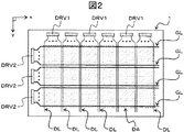
図1(a)は、液晶表示パネルの概略構成の一例を示す模式平面図である。図1(b)は、図1(a)に示した液晶表示パネルのA−A’線における断面構成の一例を示す模式断面図である。図2は、本発明の適用が望まれるTFT基板の概略構成の一例を示す模式平面図である。図3は、液晶表示パネルの1画素の回路構成の一例を示す模式回路図である。
Fig.1 (a) thru | or FIG. 3 is a schematic diagram which shows an example of schematic structure of the display panel (display apparatus) in connection with this invention.
FIG. 1A is a schematic plan view illustrating an example of a schematic configuration of a liquid crystal display panel. FIG. 1B is a schematic cross-sectional view illustrating an example of a cross-sectional configuration taken along line AA ′ of the liquid crystal display panel illustrated in FIG. FIG. 2 is a schematic plan view showing an example of a schematic configuration of a TFT substrate to which the application of the present invention is desired. FIG. 3 is a schematic circuit diagram showing an example of a circuit configuration of one pixel of the liquid crystal display panel.
本発明は、たとえば、液晶テレビ、パーソナルコンピュータ(PC)向けの液晶ディスプレイなどの液晶表示装置に用いるアクティブマトリクス型液晶表示パネル(以下、単に液晶表示パネルという)に適用される。 The present invention is applied to, for example, an active matrix liquid crystal display panel (hereinafter simply referred to as a liquid crystal display panel) used in a liquid crystal display device such as a liquid crystal television and a liquid crystal display for a personal computer (PC).
液晶表示パネルは、たとえば、図1(a)および図1(b)に示すように、第1の基板1および第2の基板2の2枚(一対)の基板の間に液晶材料3が封入されている表示パネルである。このとき、第1の基板1と第2の基板2は、映像や画像などを表示する表示領域DAの外側に設けられた環状のシール材4で接着されており、液晶材料3は、第1の基板1および第2の基板2ならびにシール材4で囲まれた空間に封入されている。また、液晶表示パネルが透過型または半透過型の場合、第1の基板1および第2の基板2の外側を向いた面には、たとえば、偏光板5A,5Bが貼り付けられている。またこのとき、第1の基板1と偏光板5Aの間、第2の基板2と偏光板5Bの間には、1層から数層の位相差板が設けられていることもある。
In the liquid crystal display panel, for example, as shown in FIG. 1A and FIG. 1B, a
液晶表示パネルの第1の基板1は、一般に、TFT基板と呼ばれており、ガラス基板などの絶縁基板の上に、複数本の走査信号線、複数本の映像信号線、表示領域DAを構成する複数の画素のそれぞれに対して配置されるTFT素子(スイッチング素子)、および画素電極などが形成されている。
The
第1の基板(以下、TFT基板という)1は、たとえば、図2に示すように、x方向に長く延びる走査信号線GLがy方向に複数本並んでおり、y方向に長く延びる映像信号線DLがx方向に複数本並んでいる。 For example, as shown in FIG. 2, the first substrate (hereinafter referred to as TFT substrate) 1 includes a plurality of scanning signal lines GL extending in the x direction, and a video signal line extending in the y direction. A plurality of DLs are arranged in the x direction.
このようなTFT基板1では、2本の隣接する走査信号線GLと2本の隣接する映像信号線DLで囲まれた領域が1つの画素領域に相当し、各画素領域にTFT素子や画素電極などが配置されている。このとき、たとえば、図3に示すように、2本の隣接する走査信号線GLm,GLm+1と、2本の隣接する映像信号線DLn,DLn+1とで囲まれた領域を画素領域とする画素に着目すると、その画素に対して配置されるTFT素子は、ゲート(G)が2本の隣接する走査信号線GLm,GLm+1のうちの一方の走査信号線GLm+1に接続されている。またこのとき、当該TFT素子は、たとえば、ドレイン(D)が2本の隣接する映像信号線DLn,DLn+1のうちの一方の映像信号線DLnに接続されており、ソース(S)が画素電極PXに接続されている。また、画素電極PXは、共通電極CT(対向電極とも呼ばれる)および液晶材料3とともに画素容量を形成している。なお、共通電極CTは、対向基板2に設けられている場合もあるし、TFT基板1に設けられている場合もある。
In such a
また、本発明は、たとえば、図2に示すように、表示領域DAの外側に、第1の駆動回路DRV1および第2の駆動回路DRV2が、内蔵回路として前記絶縁基板上に一体的に形成されているTFT基板1への適用が望まれる。第1の駆動回路DRV1および第2の駆動回路DRV2はそれぞれ、MOSトランジスタやダイオードなどの半導体素子を多数個組み合わせた集積回路であり、TFT基板1の製造過程において、走査信号線GL、映像信号線DL、表示領域DAのTFT素子などとともに形成される。以下、第1の駆動回路DRV1および第2の駆動回路DRV2のMOSトランジスタを、周辺領域のMOSトランジスタという。
In the present invention, for example, as shown in FIG. 2, a first drive circuit DRV1 and a second drive circuit DRV2 are integrally formed on the insulating substrate as a built-in circuit outside the display area DA. Application to the
第1の駆動回路DRV1は、たとえば、従来の液晶表示装置で用いられているチップ状のデータドライバICと同等の機能を有する回路であり、たとえば、各映像信号線DLに加える映像信号(階調データ)を生成する回路、生成した映像信号を各映像信号線DLに出力するタイミングを制御する回路などを有する。また、第2の駆動回路DRV2は、従来の液晶表示装置で用いられているチップ状の走査ドライバICと同等の機能を有する回路であり、たとえば、各走査信号線GLに加える走査信号を生成する回路、生成した走査信号を各走査信号線GLに出力するタイミングを制御する回路などを有する。 The first drive circuit DRV1 is a circuit having a function equivalent to, for example, a chip-shaped data driver IC used in a conventional liquid crystal display device. For example, the first drive circuit DRV1 is a video signal (gray scale) applied to each video signal line DL. Data), a circuit for controlling the timing of outputting the generated video signal to each video signal line DL, and the like. The second drive circuit DRV2 is a circuit having a function equivalent to that of a chip-like scan driver IC used in a conventional liquid crystal display device, and generates, for example, a scan signal to be applied to each scan signal line GL. A circuit and a circuit for controlling the timing of outputting the generated scanning signal to each scanning signal line GL.
またこのとき、第1の駆動回路DRV1および第2の駆動回路DRV2は、シール材4よりも内側、すなわちシール材4と表示領域DAの間に形成することが望ましいが、シール材4と平面でみて重なる領域やシール材4の外側に形成されていてもよい。
At this time, the first drive circuit DRV1 and the second drive circuit DRV2 are preferably formed inside the
図4(a)乃至図4(c)は、本発明の概要を説明するための模式図である。
図4(a)は、本発明を適用したTFT基板における表示領域のTFT素子の概略構成の一例を示す模式平面図である。図4(b)は、本発明を適用したTFT基板における周辺回路のMOSトランジスタの概略構成の一例を示す模式平面図である。図4(c)は、図4(a)のB−B’線における断面構成の一例および図4(b)のC−C’線における断面構成の一例を横に並べて示した模式断面図である。なお、図4(c)において、(n+)は高濃度のn型不純物領域であることを示している。
FIG. 4A to FIG. 4C are schematic diagrams for explaining the outline of the present invention.
FIG. 4A is a schematic plan view showing an example of a schematic configuration of a TFT element in a display region in a TFT substrate to which the present invention is applied. FIG. 4B is a schematic plan view showing an example of a schematic configuration of the MOS transistor of the peripheral circuit in the TFT substrate to which the present invention is applied. 4C is a schematic cross-sectional view illustrating an example of a cross-sectional configuration taken along line BB ′ in FIG. 4A and an example of a cross-sectional configuration taken along line CC ′ in FIG. 4B. is there. In FIG. 4C, (n +) indicates a high concentration n-type impurity region.
本発明は、図2および図3に示したような構成のTFT基板1において、表示領域DAのTFT素子(MOSトランジスタ)や、周辺領域のMOSトランジスタをボトムゲート型と呼ばれる構成、すなわち、ガラス基板などの基板と半導体層の間に各トランジスタのゲート電極が設けられている構成にする場合に適用される。
In the
このとき、表示領域DAの各画素に対して配置されるMOSトランジスタ(TFT素子)は、たとえば、図4(a)および図4(c)に示すような構成になっており、ガラス基板100の表面に形成された下地絶縁層101の上にゲート電極GP1が形成されている。ゲート電極GP1は、たとえば、走査信号線GLと一体であり、走査信号線GLの幅(y方向の寸法)を部分的に広くして設けた矩形状の突出部分を利用している。
At this time, the MOS transistor (TFT element) arranged for each pixel in the display area DA has a configuration as shown in FIGS. 4A and 4C, for example. A gate electrode GP1 is formed on the
また、ガラス基板100からみてゲート電極GP1の上には、TFT素子のゲート絶縁膜としての機能を有する第1の絶縁層102を介して半導体層SC1が形成されている。半導体層SC1は、ドレイン領域SC1a、ソース領域SC1b、およびチャネル領域SC1cの3つの領域からなり、3つの領域すべてがアモルファスシリコンなどのアモルファス半導体で形成されている。TFT素子がNチャネルMOSトランジスタの場合、半導体層SC1のドレイン領域SC1aおよびソース領域SC1bは、たとえば、不純物としてP+(リンイオン)を注入したn型のアモルファス半導体である。また、NチャネルMOSトランジスタの場合、チャネル領域SC1cは真性(i型)のアモルファス半導体、または不純物濃度が非常に低いn型のアモルファス半導体、もしくは不純物濃度が非常に低いp型のアモルファス半導体のうちのいずれか1つである。
In addition, a semiconductor layer SC1 is formed on the gate electrode GP1 as viewed from the
また、ガラス基板100からみて半導体層SC1のドレイン領域SC1aの上にはドレイン電極SD1aが形成され、ソース領域SC1bの上にはソース電極SD1bが形成されている。ドレイン電極SD1aは、たとえば、映像信号線DLと一体であり、映像信号線DLの幅(x方向の寸法)を部分的に広くして設けた矩形状の突出部分を利用している。
Further, when viewed from the
また、ガラス基板100からみてドレイン電極SD1aおよびソース電極SD1bなどのさらに上には、第2の絶縁層103および第3の絶縁層104を介して画素電極PXが形成されている。画素電極PXは、スルーホールTHによりソース電極SD1bと接続している。
In addition, the pixel electrode PX is formed on the drain electrode SD1a and the source electrode SD1b as viewed from the
またこのとき、周辺領域のMOSトランジスタ、たとえば、第1の駆動回路DRV1のMOSトランジスタは、図4(b)および図4(c)に示したような構成になっており、ガラス基板100の表面に形成された下地絶縁層101の上にゲート電極GP2が形成されている。なお、本発明を適用したTFT基板1では、周辺領域のMOSトランジスタのゲート電極GP2の厚さが、表示領域DAのTFT素子のゲート電極GP1の厚さよりも薄くなっている。
At this time, the MOS transistor in the peripheral region, for example, the MOS transistor of the first drive circuit DRV1 is configured as shown in FIGS. 4B and 4C, and the surface of the
また、ガラス基板100からみてゲート電極GP2の上には、第1の絶縁層102を介して半導体層SC2が形成されている。半導体層SC2は、ドレイン領域SC2a、ソース領域SC2b、およびチャネル領域SC2cの3つの領域からなり、ドレイン領域SC2aおよびソース領域SC2bはアモルファスシリコンなどのアモルファス半導体で形成されており、チャネル領域SC2cは多結晶シリコンなどの多結晶半導体で形成されている。周辺領域のMOSトランジスタがNチャネルMOSトランジスタの場合、半導体層SC2のドレイン領域SC2aおよびソース領域SC2bは、たとえば、不純物としてP+(リンイオン)を注入したn型のアモルファス半導体である。また、NチャネルMOSトランジスタの場合、チャネル領域SC2cは真性(i型)の多結晶半導体、または不純物濃度が非常に低いn型の多結晶半導体、もしくは不純物濃度が非常に低いp型の多結晶半導体のうちのいずれか1つである。特に、半導体層SC2のように多結晶シリコンで形成されている場合、チャネル領域SC2cに不純物をわずかに加えることで、MOSトランジスタのしきい値の制御が可能になる。
In addition, a semiconductor layer SC2 is formed on the gate electrode GP2 as viewed from the
また、ガラス基板100からみて半導体層SC2のドレイン領域SC2aの上にはドレイン電極SD2aが形成され、ソース領域SC2bの上にはソース電極SD2bが形成されている。
Further, the drain electrode SD2a is formed on the drain region SC2a of the semiconductor layer SC2 when viewed from the
また、ガラス基板100からみてドレイン電極SD2aおよびソース電極SD2bのさらに上には、第2の絶縁層103および第3の絶縁層104が形成されている。
In addition, a second insulating
本発明は、上記のように、表示領域DA(第1の領域)のTFT素子(MOSトランジスタ)と、周辺領域(第2の領域)のMOSトランジスタが、それぞれ、ガラス基板と半導体層の間にゲート電極を有するボトムゲート型であり、かつ、表示領域DAのMOSトランジスタの半導体層SC1の各領域をアモルファスシリコンなどのアモルファス半導体で形成し、周辺領域のMOSトランジスタの半導体層SC2のチャネル領域SC2cを多結晶シリコンなどの多結晶半導体で形成する場合に適用される。 In the present invention, as described above, the TFT element (MOS transistor) in the display area DA (first area) and the MOS transistor in the peripheral area (second area) are respectively disposed between the glass substrate and the semiconductor layer. Each region of the semiconductor layer SC1 of the MOS transistor in the display region DA that is a bottom gate type having a gate electrode is formed of an amorphous semiconductor such as amorphous silicon, and a channel region SC2c of the semiconductor layer SC2 of the MOS transistor in the peripheral region is formed. This is applied when forming with a polycrystalline semiconductor such as polycrystalline silicon.
以下、本発明が適用された液晶表示装置のTFT基板1における表示領域DAおよび周辺領域SAの各MOSトランジスタのゲート電極GP1,GP2の構成および製造方法について説明する。
Hereinafter, the configuration and manufacturing method of the gate electrodes GP1 and GP2 of the MOS transistors in the display area DA and the peripheral area SA in the
図5は、本発明による実施例1のTFT基板の特徴を示す模式断面図である。なお、図5において、一点鎖線の右側は表示領域DAに形成されるTFT素子(MOSトランジスタ)のゲート電極GP1の断面構成の一例を示しており、一点鎖線の左側は周辺領域SAに形成されるMOSトランジスタのゲート電極GP2の断面構成の一例を示している。 FIG. 5 is a schematic cross-sectional view showing the characteristics of the TFT substrate of Example 1 according to the present invention. In FIG. 5, the right side of the alternate long and short dash line shows an example of a cross-sectional configuration of the gate electrode GP1 of the TFT element (MOS transistor) formed in the display area DA, and the left side of the alternate long and short dash line is formed in the peripheral area SA. An example of a cross-sectional configuration of the gate electrode GP2 of the MOS transistor is shown.
実施例1のTFT基板1は、たとえば、図5に示すように、周辺領域SAに配置された第1の駆動回路DRV1などのMOSトランジスタのゲート電極GP2の厚さd2が、表示領域DAのTFT素子のゲート電極GP1の厚さd1よりも薄い。このとき、表示領域DAのTFT素子のゲート電極GP1は、周辺領域SAのMOSトランジスタのゲート電極GP2に用いられている第1の導電層601の上に、厚さd3の第2の導電層602が積層された構成になっている。
As shown in FIG. 5, for example, the
実施例1において、周辺領域SAのMOSトランジスタのゲート電極GP2および表示領域DAのTFT素子のゲート電極GP1の下層に用いられている第1の導電層601と、表示領域DAのTFT素子のゲート電極GP1のみに用いられている第2の導電層602は、同じ材料であってもよいし、異なる材料であってもよい。ただし、第1の導電層601の材料と第2の導電層602の材料との組み合わせは、第1の導電層601の材料の熱伝導率が第2の導電層602の材料の熱伝導率よりも低いことが望ましい。またこのとき、第2の導電層602の材料の電気抵抗(配線抵抗)が第1の導電層601の材料の電気抵抗(配線抵抗)よりも低い組み合わせであると、さらに望ましい。
In the first embodiment, the first
図6は、実施例1のTFT基板のゲート電極の製造方法を説明するための模式断面図である。なお、図6には、ゲート電極を形成する手順において特徴となる部分のみを(s1)から(s5)として示している。また、図6において、一点鎖線の右側は表示領域DAに形成されるTFT素子(MOSトランジスタ)のゲート電極GP1の形成手順を示しており、一点鎖線の左側は周辺領域SAに形成されるMOSトランジスタのゲート電極GP2の形成手順を示している。 6 is a schematic cross-sectional view for explaining the method for manufacturing the gate electrode of the TFT substrate of Example 1. FIG. In FIG. 6, only portions that are characteristic in the procedure for forming the gate electrode are shown as (s1) to (s5). In FIG. 6, the right side of the alternate long and short dash line shows the procedure for forming the gate electrode GP1 of the TFT element (MOS transistor) formed in the display area DA, and the left side of the alternate long and short dash line shows the MOS transistor formed in the peripheral area SA. The forming procedure of the gate electrode GP2 is shown.
実施例1のTFT基板1の製造方法において、表示領域DAのTFT素子のゲート電極GP1および周辺領域SAのMOSトランジスタのゲート電極GP2を形成する工程は、まず、図6の(s1)に示すように、ガラス基板100(絶縁基板)上に、たとえば、シリコン窒化膜(SiN膜)などの下地絶縁層101を成膜した後、第1の導電層601および第2の導電層602を続けて成膜する。
In the manufacturing method of the
次に、図6の(s2)に示すように、第2の導電層602の上のうちの、表示領域DAの上のみにレジスト701を形成した後、そのレジスト701をマスクにしてエッチングを行い、表示領域DAの外側(周辺領域SAなど)にある第2の導電層602を除去する。
Next, as shown in FIG. 6 (s2), after a resist 701 is formed only on the display area DA in the second
次に、レジスト701を除去した後、図6の(s3)に示すように、表示領域DAおよび周辺領域SAのゲート電極を形成する領域に別のレジスト702を形成する。 Next, after removing the resist 701, another resist 702 is formed in a region where the gate electrode of the display area DA and the peripheral area SA is formed, as shown in (s3) of FIG.
次に、図6の(s4)に示すように、レジスト702をマスクにしてエッチングを行い、表示領域DAは第2の導電層602および第1の導電層601の不要な部分を除去し、周辺領域SAは第1の導電層601の不要な部分を除去する。
Next, as shown in FIG. 6 (s4), etching is performed using the resist 702 as a mask, and the display area DA is formed by removing unnecessary portions of the second
その後、レジスト702を除去すると、図6の(s5)に示すように、表示領域DAには第1の導電層601および第2の導電層602が積層したゲート電極GP1が形成され、周辺領域SAには第1の導電層601のみからなる薄いゲート電極GP2が形成される。
Thereafter, when the resist 702 is removed, the gate electrode GP1 in which the first
なお、図6に示したような手順でゲート電極GP1,GP2を形成する場合、前記第1の導電層601および第2の導電層602は、同じ材料であってもよいが、異なる材料であるほうが望ましい。特に、周辺領域SAのMOSトランジスタのゲート電極GP2に用いる第1の導電層601は、半導体層SC2のチャネル領域SC2cに用いる多結晶シリコンを形成する工程で高温になるので、第1の導電層601には高融点金属材料を用いることが望ましい。
Note that when the gate electrodes GP1 and GP2 are formed by the procedure shown in FIG. 6, the first
第1の導電層601および第2の導電層602に同じ材料を用いる場合、その材料としては、たとえば、MoW合金が挙げられる。しかしながら、第1の導電層601および第2の導電層602に同じ材料を用いた場合、図6の(s2)に示した工程、すなわち周辺領域SAにある第2の導電層602をエッチングするときに第2の導電層602のみを除去することが難しい。そのため、第1の導電層601の表面もエッチングされるおそれがあり、周辺領域SAのゲート電極GP2の平坦性が悪くなる可能性がある。
In the case where the same material is used for the first
このことから、第1の導電層601には、たとえば、第2の導電層602よりも融点が高く、熱伝導率が低い材料を用いることが望ましい。また、第1の導電層601には、たとえば、第2の導電層602のエッチングに用いるエッチング液に対して不溶性または難溶性を示す材料を用いることが望ましい。またさらに、第1の導電層601は、たとえば、第2の導電層よりも電気伝導率が低い材料を用いることが望ましい。このような条件を満たす材料の組み合わせとしては、たとえば、第1導電層601をTa,Ti(チタン),MoWのいずれかにし、第2の導電層602をAl(アルミニウム)にする組み合わせがある。
For this reason, it is desirable to use a material having a higher melting point and lower thermal conductivity than the second
図7(a)乃至図8(b)は、実施例1のTFT基板の半導体層の製造方法を説明するための模式断面図である。
図7(a)は、アモルファスシリコン膜を成膜した直後の基板の概略構成を示す模式平面図である。図7(b)は、図7(a)のD−D’線における模式断面図である。図7(c)は、図7(b)に示した断面図において、周辺領域のMOSトランジスタのゲート電極が形成された領域と表示領域のTFT素子のゲート電極が形成された領域を拡大して並べた模式断面図である。図8(a)は、アモルファスシリコンを多結晶シリコン化する方法の一例を示す模式斜視図である。図8(b)は、多結晶シリコン化された領域の半導体層の概略構成を示す模式平面図である。
なお、図7(c)および図9において、一点鎖線の右側は表示領域DAに形成されるTFT素子(MOSトランジスタ)のゲート電極GP1の周辺における断面構成の一例を示しており、一点鎖線の左側は周辺領域SAに形成されるMOSトランジスタのゲート電極GP2の周辺における断面構成の一例を示している。
FIGS. 7A to 8B are schematic cross-sectional views for explaining a method for manufacturing a semiconductor layer of the TFT substrate of Example 1. FIG.
FIG. 7A is a schematic plan view showing a schematic configuration of a substrate immediately after forming an amorphous silicon film. FIG.7 (b) is a schematic cross section in the DD 'line of Fig.7 (a). FIG. 7C is an enlarged view of the region where the gate electrode of the MOS transistor in the peripheral region is formed and the region where the gate electrode of the TFT element is formed in the display region in the cross-sectional view shown in FIG. It is the arranged schematic cross section. FIG. 8A is a schematic perspective view showing an example of a method for converting amorphous silicon into polycrystalline silicon. FIG. 8B is a schematic plan view showing a schematic configuration of the semiconductor layer in the polycrystalline siliconized region.
In FIG. 7C and FIG. 9, the right side of the alternate long and short dash line shows an example of a cross-sectional configuration around the gate electrode GP1 of the TFT element (MOS transistor) formed in the display area DA. Shows an example of a cross-sectional configuration around the gate electrode GP2 of the MOS transistor formed in the peripheral region SA.
実施例1の液晶表示装置(TFT基板1)を製造するときに用いるガラス基板100は、たとえば、図7(a)に示すように、TFT基板1として用いるときの大きさよりも大きいマザーガラスと呼ばれるガラス基板100を用いて製造される。そして、マザーガラス100の上に前記手順でゲート電極GP1,GP2を形成した後、続けて、第1の絶縁層102、半導体層SC1,SC2、映像信号線DL(ドレイン電極SD1aを含む)およびソース電極SD1b、画素電極PXなどを形成し、最後にマザーガラス100から領域100Aを切り出すと、図2および図3に示したような構成のTFT基板1が得られる。
The
前記手順でゲート電極GP1,GP2を形成した後は、たとえば、図7(a)および図7(b)に示すように、マザーガラス100の全面にゲート絶縁膜としての機能を有する第1の絶縁層102を成膜し、続けて、アモルファスシリコン膜SCaを成膜する。このとき、アモルファスシリコン膜SCaは、表示領域DAだけでなく、周辺領域SAを含むマザーガラス100の全面に成膜する。また、図7(b)では省略しているが、表示領域DAや、周辺領域SAのうちの第1の駆動回路を形成する領域R1および第2の駆動回路を形成する領域R2には、たとえば、図7(c)に示すように、ゲート電極GP1,GP2や走査信号線GLなどが形成されている。そのため、アモルファスシリコン膜SCaは、たとえば、ゲート電極GP1,GP2の上にある部分と、その外側にある部分の境目に、各ゲート電極GP1,GP2の厚さに応じた段差が生じている。
After forming the gate electrodes GP1 and GP2 in the above procedure, for example, as shown in FIGS. 7A and 7B, the first insulation having a function as a gate insulating film on the entire surface of the
実施例1のTFT基板1の製造方法では、アモルファスシリコン膜SCaを成膜した後、たとえば、周辺領域SAの全域、または第1の駆動回路を形成する領域R1および第2の駆動回路を形成する領域R2のアモルファスシリコン膜SCaを多結晶シリコン化する。
In the manufacturing method of the
アモルファスシリコン膜SCaを多結晶シリコン化するときには、たとえば、エキシマレーザや連続発振レーザなどのエネルギービームを、多結晶シリコン化したい領域に照射してアモルファスシリコン膜SCaを溶融させた後、溶融したシリコンを結晶化させる。より具体的には、まず、多結晶シリコン化したい領域にエキシマレーザまたは連続発振レーザなどを照射して、アモルファスシリコン膜SCaを脱水素化する。そして、脱水素化したアモルファスシリコン膜に、別のレーザなどを照射して溶融させた後、結晶化させる。このとき、マザーガラス100は、たとえば、x方向およびy方向に移動可能なステージの上に載せて固定しておく。そして、たとえば、図8(a)に示すように、レーザ発振器8で発生させた連続発振レーザ9aを光学系10で所望のエネルギー密度および形状に変換し、その変換した連続発振レーザ9bをマザーガラス100のアモルファスシリコンSCaに照射する。このとき、マザーガラス100を載せたステージを、x方向およびy方向に移動させながら、マザーガラス100上における連続発振レーザ9bの照射位置を移動させ、多結晶シリコン化したい領域の全域に連続発振レーザ9bを照射する。
When the amorphous silicon film SCa is converted to polycrystalline silicon, for example, an energy beam such as an excimer laser or a continuous wave laser is irradiated to the region to be converted to polycrystalline silicon to melt the amorphous silicon film SCa, and then the molten silicon is Crystallize. More specifically, first, an amorphous silicon film SCa is dehydrogenated by irradiating an excimer laser or a continuous wave laser or the like on a region where polycrystalline silicon is desired. Then, the dehydrogenated amorphous silicon film is melted by irradiation with another laser or the like, and then crystallized. At this time, the
またこのとき、溶融したシリコンを多結晶シリコン化させるには、たとえば、照射する連続発振レーザ9bのエネルギー密度と照射領域の移動速度(走査速度)を調整すればよい。照射する連続発振レーザ9bのエネルギー密度と照射領域の移動速度(走査速度)がある条件を満たす場合、溶融したシリコンが固化する過程でラテラル成長が起こり、照射領域の移動方向に沿って長く延びる帯状結晶の集合体でなる多結晶シリコンが得られる。
At this time, in order to convert the melted silicon into polycrystalline silicon, for example, the energy density of the
また、アモルファスシリコン膜SCaを多結晶シリコン化するときには、たとえば、まず、図8(b)の上側に示すように、微結晶または粒状結晶などの微小な結晶11pの集合体でなる多結晶シリコンを形成してもよい。この場合、微小な結晶11pの集合体でなる多結晶シリコンに再度連続発振レーザ9bを照射して溶融、再結晶化させて、図8(b)の下側に示すように、連続発振レーザ9bの照射位置の移動方向BDに沿って長く延びる帯状結晶11wの集合体でなる多結晶シリコンSCpを形成する。
When the amorphous silicon film SCa is made into polycrystalline silicon, for example, as shown in the upper side of FIG. 8B, first, polycrystalline silicon composed of an aggregate of
このような帯状結晶11wの集合体でなる多結晶シリコンSCpを形成した場合、帯状結晶11wの長く延びる方向がチャネル長の方向、すなわちMOSトランジスタにおけるキャリアの移動方向になるようにドレイン電極SD2aおよびソース電極SD2bを形成すれば、キャリアの移動を阻害する結晶粒界がほとんど無く、各駆動回路DRV1,DRV2のMOSトランジスタを高速で動作させることができる。
When the polycrystalline silicon SCp formed of such an aggregate of the band-
上記のような手順で周辺領域SAのアモルファスシリコン膜SCaを多結晶シリコンSCpにした後の、TFT基板の製造方法(手順)について、以下、簡単に説明する。 A TFT substrate manufacturing method (procedure) after the amorphous silicon film SCa in the peripheral area SA is made to be polycrystalline silicon SCp by the above procedure will be briefly described below.
周辺領域SAのアモルファスシリコン膜SCaを多結晶シリコンSCpにしたら、次に、たとえば、マザーガラス100の全面にn型のアモルファスシリコン膜を成膜し、当該n型のアモルファスシリコン膜、アモルファスシリコン膜SCaおよび多結晶シリコンSCpを島状にパターニングする。
If the amorphous silicon film SCa in the peripheral region SA is changed to the polycrystalline silicon SCp, then, for example, an n-type amorphous silicon film is formed on the entire surface of the
次に、マザーガラス100の全面に導電膜を成膜し、当該導電膜をパターニングして映像信号線DL、ドレイン電極SD1a,SD2a、およびソース電極SD1b,SD2bなどを形成する。
Next, a conductive film is formed on the entire surface of the
次に、ドレイン電極SD1a,SD2a、およびソース電極SD1b,SD2bをマスクにして、アモルファスシリコン膜SCaおよび多結晶シリコン膜SCpの上にあるn型のアモルファスシリコン膜をエッチングする。このとき、アモルファスシリコン膜SCaの上にあるn型のアモルファスシリコン膜はドレイン領域SC1aとソース領域SC1bに分離され、多結晶シリコン膜SCpの上にあるn型のアモルファスシリコン膜はドレイン領域SC2aとソース領域SC2bに分離される。またこのとき、n型のアモルファスシリコン膜をエッチングすると、たとえば、図4(c)に示したように、アモルファスシリコン膜SCaおよび多結晶シリコンSCpの一部も除去されて薄くなる。このような手順で半導体層を形成することにより、表示領域DAのTFT素子の半導体層SC1は、ドレイン領域SC1a、ソース領域SC1b、およびチャネル領域SC1cがともにアモルファスシリコンで形成された半導体層になる。一方、周辺領域SAのMOSトランジスタの半導体層SC2は、ドレイン領域SC2aおよびソース領域SC2bがアモルファスシリコンで形成され、チャネル領域SC1cが多結晶シリコンで形成された半導体層になる。 Next, the n-type amorphous silicon film on the amorphous silicon film SCa and the polycrystalline silicon film SCp is etched using the drain electrodes SD1a and SD2a and the source electrodes SD1b and SD2b as a mask. At this time, the n-type amorphous silicon film on the amorphous silicon film SCa is separated into the drain region SC1a and the source region SC1b, and the n-type amorphous silicon film on the polycrystalline silicon film SCp is separated into the drain region SC2a and the source. It is separated into region SC2b. At this time, if the n-type amorphous silicon film is etched, for example, as shown in FIG. 4C, a part of the amorphous silicon film SCa and the polycrystalline silicon SCp is also removed and thinned. By forming the semiconductor layer in such a procedure, the semiconductor layer SC1 of the TFT element in the display area DA becomes a semiconductor layer in which the drain region SC1a, the source region SC1b, and the channel region SC1c are all formed of amorphous silicon. On the other hand, the semiconductor layer SC2 of the MOS transistor in the peripheral region SA is a semiconductor layer in which the drain region SC2a and the source region SC2b are formed of amorphous silicon and the channel region SC1c is formed of polycrystalline silicon.
また、その後は、第2の絶縁層103および第3の絶縁層104を成膜し、スルーホールTHを形成した後、たとえば、ITOなどの光透過率が高い導電膜を成膜し、当該導電膜(ITO膜)をパターニングして画素電極PXを形成する。
After that, after forming the second insulating
図9は、実施例1のTFT基板の製造方法の作用効果を説明するための模式断面図である。 FIG. 9 is a schematic cross-sectional view for explaining the function and effect of the manufacturing method of the TFT substrate of Example 1.
前述のアモルファスシリコン膜SCaを多結晶シリコン化する工程は、たとえば、連続発振レーザなどのエネルギービームを照射してアモルファスシリコン膜SCaを加熱し、溶融させる必要がある。このとき、たとえば、周辺領域SAのアモルファスシリコン膜SCaに連続発振レーザを照射すると、たとえば、図9に示すように、周辺領域SAのゲート電極GP2の上にあるアモルファスシリコンSCaに照射されたエネルギービームによる熱が、第1の絶縁膜102を介してゲート電極GP2に伝導する。このとき、ゲート電極GP2の上にある部分と、その外側にある部分でアモルファスシリコンSCaが受ける熱量(エネルギー)の総量に差が生じ、結晶性にばらつきが生じることがある。そのため、実施例1のTFT基板1の製造方法のように、レーザが照射される領域(多結晶シリコン化する領域)のゲート電極GP2を薄く形成して熱伝導の量を小さくすると、ゲート電極GP2の上にある部分と、その外側にある部分でアモルファスシリコン膜SCaが受ける熱量の総量の差を小さくでき、結晶性のばらつきを低減できる。この効果は、ゲート電極GP2に用いる第1の導電層601の熱伝導率が低いほど大きく、また、膜厚が薄いほど大きい。
In the step of converting the amorphous silicon film SCa into polycrystalline silicon, for example, it is necessary to heat and melt the amorphous silicon film SCa by irradiation with an energy beam such as a continuous wave laser. At this time, for example, when the amorphous silicon film SCa in the peripheral region SA is irradiated with a continuous wave laser, for example, as shown in FIG. 9, the energy beam irradiated to the amorphous silicon SCa on the gate electrode GP2 in the peripheral region SA. Heat is transferred to the gate electrode GP2 through the first insulating
また、実施例1のTFT基板1の製造方法のように、レーザが照射される領域(多結晶シリコン化する領域)のゲート電極GP2を薄く形成すると、ゲート電極GP2の上にある部分と、その外側にある部分の境目に生じるアモルファスシリコン膜SCaの段差を小さく(低く)することができる。そのため、レーザを照射してアモルファスシリコン膜SCaを溶融させたときに、段差の上の部分から下の部分に流れ落ちる溶融シリコンの量を少なくでき、段差部分での膜剥れを低減することができる。この効果は、ゲート電極GP2に用いる第1の導電層601の膜厚が薄いほど大きい。
Further, as in the method of manufacturing the
また、実施例1のTFT基板の製造方法では、レーザが照射される領域、すなわち高速での動作が要求される第1の駆動回路DRV1を形成する領域R1および第2の駆動回路DRV2を形成する領域R2のMOSトランジスタのゲート電極GP2のみを薄くでき、表示領域DAのTFT素子のゲート電極GP1は、従来の液晶表示装置(TFT基板)におけるゲート電極と同程度の厚さにすることができる。そのため、たとえば、ゲート電極GP1と一体の走査信号線GLを形成する場合、走査信号線GLの配線抵抗が高くなるのを防ぎ、消費電力の増大や画素部の信号遅延による動作不良を低減することができる。走査信号線GLは、その一端が表示領域DAの外側にある第2の駆動回路DRV2を形成する領域R2まで延びているが、表示領域DAを通る部分の配線長のほうが長い。そのため、走査信号線GLのうちの表示領域DAを通る部分をゲート電極GP1と同じ積層構成にすることで、配線抵抗を小さくする効果が大きくなる。またこのとき、第1の導電層601と第2の導電層602が同じ材料でも配線抵抗を小さくする効果は得られるが、第2の導電層602に、第1の導電層601よりも電気伝導率が高い材料を用いと、さらに大きな効果が得られる。また、第2の導電層602は、第1の導電層601に比べて融点の低い材料を用いることも可能であり、たとえば、Alを用いることもできる。
Further, in the TFT substrate manufacturing method according to the first embodiment, the region to be irradiated with the laser, that is, the region R1 for forming the first drive circuit DRV1 that is required to operate at high speed, and the second drive circuit DRV2 are formed. Only the gate electrode GP2 of the MOS transistor in the region R2 can be made thin, and the gate electrode GP1 of the TFT element in the display region DA can be made as thick as the gate electrode in the conventional liquid crystal display device (TFT substrate). Therefore, for example, when the scanning signal line GL integrated with the gate electrode GP1 is formed, it is possible to prevent the wiring resistance of the scanning signal line GL from increasing, and to reduce malfunction due to increase in power consumption or signal delay of the pixel portion. Can do. One end of the scanning signal line GL extends to the region R2 that forms the second drive circuit DRV2 outside the display region DA, but the wiring length of the portion passing through the display region DA is longer. Therefore, the effect of reducing the wiring resistance is increased by making the portion of the scanning signal line GL that passes through the display area DA the same stacked structure as the gate electrode GP1. At this time, even if the first
また、実施例1のTFT基板の製造方法では、表示領域DAのTFT素子(MOSトランジスタ)および周辺領域SAのMOSトランジスタのゲート絶縁膜102の膜厚を厚くしなくても、ゲート電極GP2の熱伝導の影響による多結晶シリコン膜の結晶性のばらつきを小さくできる。そのため、ゲート絶縁膜の膜厚を厚くすることにより生じる別の問題、たとえば、トランジスタ特性のうちのIONの低下、Vthのばらつきの増加という問題や、生産性の低下といった問題を回避できる。
Further, in the manufacturing method of the TFT substrate of Example 1, the heat of the gate electrode GP2 can be obtained without increasing the film thickness of the TFT element (MOS transistor) in the display area DA and the
図10(a)および図10(b)は、実施例1のTFT基板の製造方法の変形例を説明するための模式断面図である。なお、図10(a)および図10(b)には、ゲート電極を形成する手順において特徴となる部分のみを(s11)から(s16)として示している。また、図10(a)および図10(b)において、一点鎖線の右側は表示領域DAに形成されるTFT素子(MOSトランジスタ)のゲート電極GP1の形成手順を示しており、一点鎖線の左側は周辺領域SAに形成されるMOSトランジスタのゲート電極GP2の形成手順を示している。 FIG. 10A and FIG. 10B are schematic cross-sectional views for explaining a modification of the manufacturing method of the TFT substrate of Example 1. FIG. In FIGS. 10A and 10B, only portions that are characteristic in the procedure of forming the gate electrode are shown as (s11) to (s16). 10 (a) and 10 (b), the right side of the alternate long and short dash line shows the procedure for forming the gate electrode GP1 of the TFT element (MOS transistor) formed in the display area DA, and the left side of the alternate long and short dash line is A procedure for forming the gate electrode GP2 of the MOS transistor formed in the peripheral region SA is shown.
実施例1のTFT基板の製造方法において、ゲート電極GP1,GP2を形成する手順としては、たとえば、図6に示したように、1つめのレジスト701で表示領域DAの外側にある第2の導電層602を除去し、2つめのレジスト702でゲート電極GP1,GP2をパターニングする手順が考えられる。しかしながら、この手順では、1つめのレジスト701を形成する際と、2つめのレジスト702を形成する際に、それぞれ異なるマスクを用いて露光、現像する必要があるので生産性が悪い。そこで、実施例1のTFT基板1のゲート電極GP1,GP2を形成するときには、たとえば、ハーフ露光またはハーフトーン露光と呼ばれる露光技術を用いてレジストを形成し、1回の露光、現像で形成したレジストで周辺領域SAの第2の導電層602の除去と、ゲート電極GP1,GP2のパターニングを行うことが望ましい。
In the manufacturing method of the TFT substrate according to the first embodiment, as a procedure for forming the gate electrodes GP1 and GP2, for example, as shown in FIG. 6, the second conductive material outside the display area DA with the first resist 701 is used. A procedure for removing the
ハーフ露光技術を用いたレジストでゲート電極GP1,GP2を形成するときにも、まず、図10(a)の(s11)に示すように、ガラス基板100(絶縁基板)上のシリコン窒化膜(SiN膜)などの下地絶縁層101を成膜した後、第1の導電層601および第2の導電層602を続けて成膜する。
Also when forming the gate electrodes GP1 and GP2 with a resist using the half exposure technique, first, as shown in (s11) of FIG. 10A, a silicon nitride film (SiN) on the glass substrate 100 (insulating substrate). After the
次に、図10(a)の(s12)に示すように、第2の導電層602の上に塗布した感光性レジスト703に対してハーフ露光を行う。ハーフ露光を行うときには、たとえば、周辺領域SAの薄いゲート電極GP2を形成する領域の光の透過量が、表示領域DAのゲート電極GP1を形成する領域の光の透過量よりも小さくなるようにしたマスク(図示しない)を用い、各領域に照射される光12(たとえば紫外線)の光量を変化させる。このとき、たとえば、表示領域DAのゲート電極GP1を形成する領域のレジスト703が完全に感光する最短時間で露光を終了すると、周辺領域SAの薄いゲート電極GP2を形成する領域のレジスト703は不完全な状態で感光が終了する。そのため、このレジスト703を現像すると、たとえば、図10(a)の(s13)に示すように、周辺領域SAの薄いゲート電極GP2を形成する領域におけるレジスト703bの膜厚が、表示領域DAのゲート電極GP1を形成する領域におけるレジスト703aの膜厚よりも薄くなる。
Next, as shown in (s12) of FIG. 10A, half exposure is performed on the photosensitive resist 703 coated on the second
なお、図10(a)の(s12)および(s13)に示した手順では、ネガ型の感光性レジストを用いてレジスト703a,703bを形成する場合を例を挙げているが、これに限らず、たとえば、ポジ型の感光性レジストを用いてレジスト703a,703bを形成することも可能である。 In the procedure shown in (s12) and (s13) of FIG. 10A, an example is given in which the resists 703a and 703b are formed using a negative photosensitive resist. However, the present invention is not limited to this. For example, the resists 703a and 703b can be formed using a positive photosensitive resist.
次に、図10(a)の(s14)に示すように、表示領域DAのゲート電極GP1を形成する領域のレジスト703a、および周辺領域SAの薄いゲート電極GP2を形成する領域のレジスト703bをマスクにして、各領域の第2の導電層602および第1の導電層601のうちの不要な部分を除去する。このとき、周辺領域SAの薄いゲート電極は、平面でみた形状は最終的なゲート電極GP2と同じパターンであるが、まだ第2の導電層602(不要な導電層)が残っている状態である。
Next, as shown in (s14) of FIG. 10A, the resist 703a in the region for forming the gate electrode GP1 in the display region DA and the resist 703b in the region for forming the thin gate electrode GP2 in the peripheral region SA are masked. Thus, unnecessary portions of the second
そこで、次に、たとえば、O2アッシングを行い、図10(b)の(s15)に示すように、マザーガラス100に形成されているすべてのレジスト703a,703bを、周辺領域SAの薄いゲート電極GP2を形成する部分にあるレジスト703bの厚さd4の分だけ薄くする。このようにすると、周辺領域SAの薄いゲート電極GP2を形成する部分はレジストが無くなり、表示領域DAのゲート電極GP1を形成する部分のみにレジスト703bの厚さd4分だけ薄くなったレジスト703a’が残る。
Therefore, next, for example, O 2 ashing is performed, and as shown in (s15) of FIG. 10B, all the resists 703a and 703b formed on the
次に、たとえば、図10(b)の(s16)に示すように、O2アッシング後に残ったレジスト703a’をマスクにしたエッチングで第2の導電層602を除去すると、周辺領域SAに第1の導電層601のみからなる薄いゲート電極GP2を形成することができる。
Next, for example, as shown in (s16) of FIG. 10B, when the second
このように、ハーフ露光技術を用いれば、厚さが異なるゲート電極GP1,GP2を形成するためのレジストを露光、現像する工程を1回にすることができる。 As described above, when the half exposure technique is used, the steps of exposing and developing the resist for forming the gate electrodes GP1 and GP2 having different thicknesses can be performed once.
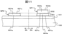
図11は、実施例1のTFT基板の応用例を説明するための模式断面図である。なお、図11において、一点鎖線の右側は表示領域DAに形成されるTFT素子(MOSトランジスタ)のゲート電極GP1の断面構成を示しており、一点鎖線の左側は周辺領域SAに形成されるMOSトランジスタのゲート電極GP2の断面構成を示している。 FIG. 11 is a schematic cross-sectional view for explaining an application example of the TFT substrate of Example 1. FIG. In FIG. 11, the right side of the alternate long and short dash line shows the cross-sectional configuration of the gate electrode GP1 of the TFT element (MOS transistor) formed in the display area DA, and the left side of the alternate long and short dash line shows the MOS transistor formed in the peripheral area SA. The cross-sectional structure of the gate electrode GP2 is shown.
実施例1では、たとえば、第1の導電層601および第2の導電層602が、それぞれ単一の材料である場合を例に挙げたが、これに限らず、第1の導電層601または第2の導電層602のいずれか一方、あるいはその両方が、2層以上の導電層を積層した構成であってもよい。すなわち、第1の導電層601のみで形成される周辺領域SAのゲート電極GP2において、当該第1の導電層601は、たとえば、図11に示すように、3つの導電層601a,601b,601cが積層された構成であってもよい。このとき、第1の導電層601および第2の導電層602で形成される表示領域DAのゲート電極GP1は、たとえば、図11に示すように、3つの導電層601a,601b,601cからなる第1の導電層601の上に、2つの導電層602a,602bからなる第2の導電層602が積層されていてもよい。このような構成の場合、たとえば、導電層601b,602aにはAlを用い、導電層601a,601c,602bにはMoまたはMoW合金を用いる。
In the first embodiment, for example, the case where the first
なお、図11に示した例は、第1の導電層601の積層構成および第2の導電層602の積層構成の組み合わせの一例であり、表示領域DAのゲート電極GP1および周辺領域SAのゲート電極GP2ならびに走査信号線GLについての電気的な特性および熱的な特性の関係が、実施例1で説明した条件を満たすものであれば、他の積層構成であってもよいことはもちろんである。
Note that the example shown in FIG. 11 is an example of a combination of the stacked configuration of the first
図12は、本発明による実施例2のTFT基板の特徴を示す模式断面図である。なお、図12において、一点鎖線の右側は表示領域DAに形成されるTFT素子(MOSトランジスタ)のゲート電極GP1の断面構成の一例を示しており、一点鎖線の左側は周辺領域SAに形成されるMOSトランジスタのゲート電極GP2の断面構成の一例を示している。 FIG. 12 is a schematic cross-sectional view showing the characteristics of the TFT substrate of Example 2 according to the present invention. In FIG. 12, the right side of the alternate long and short dash line shows an example of a cross-sectional configuration of the gate electrode GP1 of the TFT element (MOS transistor) formed in the display area DA, and the left side of the alternate long and short dash line is formed in the peripheral area SA. An example of a cross-sectional configuration of the gate electrode GP2 of the MOS transistor is shown.
実施例2のTFT基板1は、たとえば、図12に示すように、周辺領域SAに配置された第1の駆動回路DRV1などのMOSトランジスタのゲート電極GP2の厚さd2が、表示領域DAのTFT素子のゲート電極GP1の厚さd1よりも薄い。このとき、周辺領域SAのゲート電極GP2が第1の導電層601のみで形成されており、表示領域DAのゲート電極GP1が第1の導電層601と第2の導電層602とで形成されている点は、実施例1のTFT基板1と同じである。
For example, as shown in FIG. 12, the
ただし、実施例2のTFT基板1において、表示領域DAのゲート電極GP1は、第2の導電層602が、ガラス基板100(下地絶縁層101)と、第1の導電層601との間に設けられた構成になっている。
However, in the
また、実施例2においても、周辺領域SAのMOSトランジスタのゲート電極GP2および表示領域DAのTFT素子のゲート電極GP1に用いられている第1の導電層601と、表示領域DAのTFT素子のゲート電極GP1のみに用いられている第2の導電層602は、同じ材料であってもよいし、異なる材料であってもよい。ただし、第1の導電層601の材料と第2の導電層602の材料との組み合わせは、実施例1でも説明したように、第1の導電層601の熱伝導率が第2の導電層602の熱伝導率よりも低いことが望ましい、またこのとき、第2の導電層602の電気抵抗(配線抵抗)が第1の導電層601の電気抵抗(配線抵抗)よりも低い組み合わせであると、さらに望ましい。
Also in the second embodiment, the first
図13は、実施例2のTFT基板のゲート電極の製造方法を説明するための模式断面図である。なお、図13には、ゲート電極を形成する手順において特徴となる部分のみを(s21)から(s25)として示している。また、図13において、一点鎖線の右側は表示領域DAに形成されるTFT素子(MOSトランジスタ)のゲート電極GP1の形成手順を示しており、一点鎖線の左側は周辺領域SAに形成されるMOSトランジスタのゲート電極GP2の形成手順を示している。 FIG. 13 is a schematic cross-sectional view for explaining the method for manufacturing the gate electrode of the TFT substrate of Example 2. In FIG. 13, only the portions that are characteristic in the procedure of forming the gate electrode are shown as (s21) to (s25). In FIG. 13, the right side of the alternate long and short dash line shows the procedure for forming the gate electrode GP1 of the TFT element (MOS transistor) formed in the display area DA, and the left side of the alternate long and short dash line shows the MOS transistor formed in the peripheral area SA. The forming procedure of the gate electrode GP2 is shown.
実施例2のTFT基板1の製造方法において、表示領域DAのTFT素子のゲート電極GP1、第1の駆動回路DRV1および第2の駆動回路DRV2のMOSトランジスタのゲート電極GP2を形成する工程は、まず、図13の(s21)に示すように、ガラス基板(絶縁基板)100上にシリコン窒化膜(SiN膜)などの下地絶縁層101を成膜した後、第2の導電層602を成膜する。
In the manufacturing method of the
次に、図13の(s22)に示すように、第2の導電層602の上のうちの、表示領域DAの上のみにレジスト701を形成し、表示領域DAの外側(周辺領域SA)にある第2の導電層602をエッチングで除去する。
Next, as shown in (s22) of FIG. 13, a resist 701 is formed only on the display area DA of the second
次に、レジスト701を除去した後、図13の(s23)に示すように、ガラス基板100の全面、すなわち表示領域DAおよび周辺領域SAに第1の導電層601を成膜する。
Next, after removing the resist 701, as shown in (s23) of FIG. 13, the first
次に、図13の(s24)に示すように、レジスト702を形成し、レジスト702をマスクにしたエッチングを行い、表示領域DAは第1の導電層601および第2の導電層602の不要な部分を除去し、その外側の周辺領域SAは第1の導電層601の不要な部分を除去する。
Next, as shown in (s24) of FIG. 13, a resist 702 is formed, and etching is performed using the resist 702 as a mask, so that the display area DA is unnecessary for the first
その後、レジスト702を除去すると、図13の(s25)に示すように、表示領域DAには第1の導電層601および第2の導電層602が積層したゲート電極GP1が形成され、周辺領域SAには第1の導電層601のみからなる薄いゲート電極GP2が形成される。
Thereafter, when the resist 702 is removed, the gate electrode GP1 in which the first
なお、図13に示したような手順でゲート電極GP1,GP2を形成する場合、前記第2の導電層602および第1の導電層601は、同じ材料であってもよいし、異なる材料であってもよい。同じ材料を用いる場合は、たとえば、MoW合金を用いる。また、異なる材料を用いる場合は、たとえば、周辺領域SAのMOSトランジスタのゲート電極GP2にも用いられる第1の導電層601にMoW合金を用い、第2の導電層602にAlを用いる。
Note that when the gate electrodes GP1 and GP2 are formed by the procedure shown in FIG. 13, the second
また、このような手順で表示領域DAとその外側の周辺領域SAとで厚さが異なり、かつ、周辺領域SAのほうが薄くなるように各領域DA,SAのゲート電極GP1,GP2を形成した後は、アモルファスシリコン膜SCaを成膜し、たとえば、周辺領域SAのアモルファスシリコンSCaを多結晶シリコン化する。このときの手順、および得られる効果については、実施例1で説明した通りである。また、周辺領域SAのアモルファスシリコン膜SCaを多結晶シリコン化した後の工程については、実施例1で説明した手順で行えばよいので、その説明は省略する。 Further, after forming the gate electrodes GP1 and GP2 of the respective areas DA and SA so that the thickness is different between the display area DA and the peripheral area SA outside the display area DA and the peripheral area SA is thinner in such a procedure. Forms an amorphous silicon film SCa, for example, turns amorphous silicon SCa in the peripheral region SA into polycrystalline silicon. The procedure at this time and the obtained effect are as described in the first embodiment. Further, the process after the amorphous silicon film SCa in the peripheral region SA is converted to polycrystalline silicon may be performed according to the procedure described in the first embodiment, and the description thereof is omitted.
このように、実施例2のTFT基板1の製造方法においても、周辺領域SAのMOSトランジスタを形成する領域のアモルファスシリコンSCaを多結晶シリコン化したときに、ゲート電極GP2の上にある部分とその外側にある部分の結晶性のばらつきや、段差部分での膜剥がれを低減することができる。
Thus, also in the manufacturing method of the
また、表示領域DAのTFT素子のゲート電極GP1や走査信号線GLの配線抵抗が高くなるのを防ぎ、消費電力の増大や画素部の信号遅延による不良を低減することができる。 In addition, it is possible to prevent the wiring resistance of the gate electrode GP1 and the scanning signal line GL of the TFT element in the display area DA from increasing, and to reduce defects due to an increase in power consumption and a signal delay in the pixel portion.
また、各領域のTFT素子(MOSトランジスタ)のゲート絶縁膜102の膜厚を厚くすることにより生じる別の問題、たとえば、トランジスタ特性のうちのIONの低下、Vthのばらつきの増加という問題や、生産性の低下といった問題を回避できる。
Another problem caused by increasing the thickness of the
またさらに、実施例2のTFT基板1の製造方法では、表示領域DAのみに第2の導電層602を形成した後、第1の導電層601を全面に形成するので、周辺領域SAは第1の導電層601のみをエッチングすればよい。そのため、第2の導電層602と第1の導電層601が同じ材料、たとえば、MoW合金であっても、周辺領域SAのゲート電極GP2の表面の平坦性が悪くなるのを防げる。
Furthermore, in the manufacturing method of the
また、実施例2では、たとえば、第1の導電層601および第2の導電層602が、それぞれ単一の材料である場合を例に挙げたが、これに限らず、第1の導電層601または第2の導電層602のいずれか一方、あるいはその両方が、2層以上の導電層を積層した構成であってもよいことはもちろんである。
In the second embodiment, for example, the first
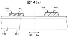
図14(a)および図14(b)は、本発明による実施例3のTFT基板の特徴を示す模式断面図である。
図14(a)は、表示領域のゲート電極と周辺領域のゲート電極との断面構成の一例を示す模式断面図である。図14(b)は、表示領域の走査信号線と周辺領域の走査信号線の接続部分の断面構成の一例を示す模式断面図である。なお、図14(a)において、一点鎖線の右側は表示領域DAに形成されるTFT素子(MOSトランジスタ)のゲート電極GP1の断面構成の一例を示しており、一点鎖線の左側は周辺領域SAに形成されるMOSトランジスタのゲート電極GP2の断面構成の一例を示している。また、図14(b)において、一点鎖線の右側は表示領域DAにおける走査信号線GLの断面構成の一例を示しており、一点鎖線の左側は周辺領域SAにおける走査信号線GLの断面構成の一例を示している。
FIG. 14A and FIG. 14B are schematic cross-sectional views showing the characteristics of the TFT substrate of Example 3 according to the present invention.
FIG. 14A is a schematic cross-sectional view showing an example of a cross-sectional configuration of the gate electrode in the display region and the gate electrode in the peripheral region. FIG. 14B is a schematic cross-sectional view illustrating an example of a cross-sectional configuration of a connection portion between the scanning signal line in the display region and the scanning signal line in the peripheral region. In FIG. 14A, the right side of the alternate long and short dash line shows an example of a cross-sectional configuration of the gate electrode GP1 of the TFT element (MOS transistor) formed in the display area DA, and the left side of the alternate long and short dash line is in the peripheral area SA. An example of a cross-sectional configuration of the gate electrode GP2 of the formed MOS transistor is shown. In FIG. 14B, the right side of the alternate long and short dash line shows an example of the cross-sectional configuration of the scanning signal line GL in the display area DA, and the left side of the alternate long and short dash line shows an example of the cross-sectional configuration of the scanning signal line GL in the peripheral region SA. Is shown.
実施例1および実施例2では、表示領域DAのTFT素子のゲート電極GP1に、周辺領域SAのMOSトランジスタのゲート電極GP2に用いる第1の導電層601が含まれている場合の構成について説明した。実施例3では、これらの構成とは異なり、表示領域DAのTFT素子のゲート電極GP1に、周辺領域SAのMOSトランジスタのゲート電極GP2に用いる第1の導電層601が含まれていない場合の構成について説明する。
In the first and second embodiments, the configuration in the case where the gate electrode GP1 of the TFT element in the display area DA includes the first
実施例3のTFT基板1は、たとえば、図14(a)に示すように、周辺領域SAに配置された第1の駆動回路DRV1などのMOSトランジスタのゲート電極GP2の厚さが、表示領域DAのTFT素子のゲート電極GP1の厚さよりも薄い。このとき、周辺領域SAのゲート電極GP2が第1の導電層601のみで形成されている点は、実施例1や実施例2のTFT基板1と同じである。
For example, as shown in FIG. 14A, the
ただし、実施例3のTFT基板1において、表示領域DAのTFT素子のゲート電極GP1は、たとえば、第2の導電層602のみで形成されている。このとき、表示領域DAのゲート電極GP1に接続されている走査信号線GLは、たとえば、図14(b)に示すように、表示領域DAを通る部分は第2の導電層602で形成され、周辺領域SAを通る部分は第1の導電層601で形成される。そして、1本の走査信号線GLを構成する第1の導電層601と第2の導電層602とは、たとえば、表示領域DAと周辺領域SAの境界あるいはその近傍で、第2の導電層602の端部が第1の導電層601の端部の上に乗り上げる形で電気的に接続される。
However, in the
実施例3のような構成のTFT基板1の製造方法において、ゲート電極GP1,GP2や走査信号線GLを形成するときには、たとえば、まず、ガラス基板100の上にシリコン窒化膜などの下地絶縁層101を成膜した後、続けて第1の導電層601を成膜する。次に、第1の導電層601の上にレジストを形成し、第1の導電層601をエッチングして、表示領域DAの外側(周辺領域SA)のみに、走査信号線GL、第1の駆動回路DRV1および第2の駆動回路DRV2のMOSトランジスタのゲート電極GP2などを形成する。
In the manufacturing method of the
次に、ガラス基板100の上に第2の導電層602を成膜する。その後、第2の導電層602の上にレジストを形成し、第2の導電層602をエッチングして、表示領域DAのみに、周辺領域SAに形成されている走査信号線GLと接続される走査信号線GL、表示領域DAのTFT素子のゲート電極GP1などを形成する。
Next, a second
このとき、たとえば、第1の導電層601の材料として、第2の導電層602(たとえば、アルミニウム)よりも熱伝導率が低い材料を用いることが望ましい。そして、第1の導電層601を第2の導電層602よりも薄く成膜してゲート電極GP2などを形成すれば、実施例1および実施例2で説明したTFT基板1と同様の効果を得ることができる。
At this time, for example, it is desirable to use a material having a lower thermal conductivity than the second conductive layer 602 (for example, aluminum) as the material of the first
なお、実施例3のような構成のTFT基板1の場合、たとえば、第1の導電層601の材料として、第2の導電層602(たとえば、アルミニウム)よりも熱伝導率が低い材料を用いるのであれば、各導電層601,602の厚さはほぼ同じであってもよいことはもちろんである。しかしながら、アモルファスシリコンSCaを多結晶シリコン化する工程で、溶融したシリコンが段差の上側から下側に流れ落ちて段差部分に膜剥れが起こるのを防ぐには、第1の導電層601を可能な限り薄く成膜することが望ましい。
In the case of the
以上、本発明を、前記実施例に基づき具体的に説明したが、本発明は、前記実施例に限定されるものではなく、その要旨を逸脱しない範囲において、種々変更可能であることはもちろんである。 The present invention has been specifically described above based on the above-described embodiments. However, the present invention is not limited to the above-described embodiments, and various modifications can be made without departing from the scope of the present invention. is there.
たとえば、TFT基板1の表示領域DAのTFT素子、第1の駆動回路DRV1および第2の駆動回路DRV2のMOSトランジスタは、ボトムゲート構造であればよく、図4(a)乃至図4(c)に示したような構造に限らず、他の構造であってもよい。
For example, the TFT elements in the display area DA of the
図15および図16(a)乃至図16(c)は、本発明のTFT基板におけるMOSトランジスタの構造の他の一例を示す模式図である。
図15は、図4(a)に示したTFT素子の平面構成の変形例を説明するための模式平面図である。
図16(a)は、本発明を適用したTFT基板における表示領域のTFT素子の概略構成の他の一例を示す模式平面図である。図16(b)は、本発明を適用したTFT基板における周辺回路のMOSトランジスタの概略構成の他の一例を示す模式平面図である。図16(c)は、図16(a)のE−E’線における断面構成の一例および図16(b)のF−F’線における断面構成の一例を横に並べて示した模式断面図である。なお、図16(c)において、(n+)は高濃度のn型不純物領域であることを示し、(n−)は低濃度のn型不純物領域であることを示している。
15 and 16 (a) to 16 (c) are schematic views showing another example of the structure of the MOS transistor in the TFT substrate of the present invention.
FIG. 15 is a schematic plan view for explaining a modification of the planar configuration of the TFT element shown in FIG.
FIG. 16A is a schematic plan view showing another example of the schematic configuration of the TFT element in the display region in the TFT substrate to which the present invention is applied. FIG. 16B is a schematic plan view showing another example of the schematic configuration of the MOS transistor of the peripheral circuit in the TFT substrate to which the present invention is applied. FIG. 16C is a schematic cross-sectional view illustrating an example of a cross-sectional configuration taken along line EE ′ of FIG. 16A and an example of a cross-sectional configuration taken along line FF ′ of FIG. is there. In FIG. 16C, (n +) indicates a high concentration n-type impurity region, and (n−) indicates a low concentration n-type impurity region.
前記実施例1乃至実施例3では、表示領域DAにおけるTFT素子の周辺を平面でみたときの構成が、たとえば、図4(a)に示したような構成になっており、走査信号線GLの幅(y方向の寸法)を部分的に広くして設けた矩形状の突出部分をゲート電極GP1として利用している。しかしながら、表示領域DAのTFT素子の平面構成は、これに限らず、たとえば、図15に示すように、走査信号線GLの幅を一定にして、当該走査信号線GLの上に半導体層SC1を設けてもよい。また、映像信号線DLについても、映像信号線DLの幅(x方向の寸法)を部分的に広くして設けた矩形状の突出部分をドレイン電極SD1aとして利用する代わりに、たとえば、図15に示すように、映像信号線DLの幅を一定にして、映像信号線DLの下に半導体層SC1を設けてもよいことはもちろんである。 In the first to third embodiments, the configuration when the periphery of the TFT element in the display area DA is viewed in plan is, for example, a configuration as shown in FIG. 4A, and the scanning signal line GL A rectangular protruding portion having a partially enlarged width (dimension in the y direction) is used as the gate electrode GP1. However, the planar configuration of the TFT elements in the display area DA is not limited to this. For example, as shown in FIG. 15, the width of the scanning signal line GL is fixed, and the semiconductor layer SC1 is formed on the scanning signal line GL. It may be provided. Further, with respect to the video signal line DL, instead of using a rectangular projecting portion provided by partially widening the width (dimension in the x direction) of the video signal line DL as the drain electrode SD1a, for example, FIG. As shown, the width of the video signal line DL may be constant and the semiconductor layer SC1 may be provided below the video signal line DL.
また、表示領域DAのTFT素子(MOSトランジスタ)や、周辺領域SAの第1の駆動回路DRV1および第2の駆動回路DRV2のMOSトランジスタをボトムゲート構成にする場合、各領域DA,SAに形成されるMOSトランジスタは、図4(a)乃至図4(c)に示したような構成に限らず、たとえば、図16(a)乃至図16(c)に示したような構成にすることもできる。このとき、表示領域DAの各画素に対して配置されるMOSトランジスタ(TFT素子)は、たとえば、図16(a)および図16(c)に示すような構成になっており、ガラス基板100の表面に形成された下地絶縁層101の上にゲート電極GP1が形成されている。ゲート電極GP1は、たとえば、走査信号線GLと一体であり、走査信号線GLの幅(y方向の寸法)を部分的に広くして設けた矩形状の突出部分を利用している。
Further, when the TFT elements (MOS transistors) in the display area DA and the MOS transistors in the first drive circuit DRV1 and the second drive circuit DRV2 in the peripheral area SA have a bottom gate configuration, they are formed in the areas DA and SA. The MOS transistor is not limited to the configuration shown in FIGS. 4A to 4C, but can be configured as shown in FIGS. 16A to 16C, for example. . At this time, the MOS transistor (TFT element) disposed for each pixel in the display area DA has a configuration as shown in FIGS. 16A and 16C, for example. A gate electrode GP1 is formed on the
また、ガラス基板100からみてゲート電極GP1の上には、第1の絶縁層(ゲート絶縁膜)102を介して半導体層SC1が形成されている。半導体層SC1は、ドレイン領域SC1a、ソース領域SC1b、およびチャネル領域SC1cの3つの領域からなり、各領域は、アモルファスシリコンなどのアモルファス半導体で形成されている。TFT素子がNチャネルMOSトランジスタの場合、半導体層SC1のドレイン領域SC1aおよびソース領域SC1bは、たとえば、不純物としてリンが注入されたn型半導体領域であり、チャネル領域SC1cは真性(i型)のアモルファス半導体、または不純物濃度が非常に低いn型のアモルファス半導体、もしくは不純物濃度が非常に低いp型のアモルファス半導体のいずれか1つである。
A semiconductor layer SC1 is formed on the gate electrode GP1 as viewed from the
また、ガラス基板100からみて半導体層SC1のさらに上には、第4の絶縁層105を介して映像信号線DLおよびソース電極SD1bが形成されており、映像信号線DLはスルーホールTH1により半導体層SC1のドレイン領域SC1aと接続しており、ソース電極SD1bはスルーホールTH2により半導体層SC1のソース領域SC1bと接続している。
In addition, a video signal line DL and a source electrode SD1b are formed via a fourth insulating
また、映像信号線DLおよびソース電極SD1bのさらに上には、第2の絶縁層103および第3の絶縁層104を介して画素電極PXが形成されている。画素電極PXは、スルーホールTH3によりソース電極SD1bと接続している。
Further, a pixel electrode PX is formed on the video signal line DL and the source electrode SD1b via the second insulating
なお、図16(a)に示した例では、映像信号線DLの幅(x方向の寸法)を一定にして、映像信号線DLと半導体層SC1とが平面でみて重なる領域にスルーホールTH1を形成しているが、これに限らず、たとえば、映像信号線DLの幅を部分的に広くした矩形状の突出部分を形成し、当該突出部分をTFT素子のドレイン電極SD1aとして利用してもよいことはもちろんである。 In the example shown in FIG. 16A, the width (dimension in the x direction) of the video signal line DL is made constant, and the through hole TH1 is formed in a region where the video signal line DL and the semiconductor layer SC1 overlap when viewed in plan. However, the present invention is not limited to this. For example, a rectangular protruding portion in which the width of the video signal line DL is partially widened may be formed, and the protruding portion may be used as the drain electrode SD1a of the TFT element. Of course.
またこのとき、周辺領域のMOSトランジスタは、たとえば、図16(b)および図16(c)に示したような構成になっており、ガラス基板100の表面に形成された下地絶縁層101の上にゲート電極GP2が形成されている。
At this time, the MOS transistor in the peripheral region has a structure as shown in FIGS. 16B and 16C, for example, and is above the
また、ガラス基板100からみてゲート電極GP2の上には、第1の絶縁層102を介して半導体層SC2が形成されている。周辺領域のMOSトランジスタをNチャネルMOSトランジスタにする場合、たとえば、よりスムーズにキャリアが移動するLDD構造(Lightly Doped Drain構造)にすることが望ましい。このとき、半導体層SC2は、2つのドレイン領域SC2a,SC2d、2つのソース領域SC2b,SC2e、およびチャネル領域SC2cの5つの領域からなり、5つの領域すべてが多結晶シリコンなどの多結晶半導体で形成されている。またこのとき、2つのドレイン領域SC2a,SC2dは、たとえば、不純物としてP+(リンイオン)が注入されたN型半導体領域であり、かつ、チャネル領域SC2cに近いほうの領域SC2dは、遠いほうの領域SC2aよりも不純物濃度が低い。同様に、2つのソース領域SC2b,SC2eも、たとえば、不純物としてP+(リンイオン)が注入されたN型半導体領域であり、かつ、チャネル領域SC2cに近いほうの領域SC2eは、遠いほうの領域SC2bよりも不純物濃度が低い。また、チャネル領域SC2cは真性(i型)の多結晶半導体、または不純物濃度が非常に低いn型の多結晶半導体、もしくは不純物濃度が非常に低いp型の多結晶半導体のうちのいずれか1つである。特に、半導体層SC2のように多結晶半導体(多結晶シリコン)で形成されている場合、チャネル領域SC2cに不純物をわずかに加えることで、MOSトランジスタのしきい値の制御が可能になる。
In addition, a semiconductor layer SC2 is formed on the gate electrode GP2 as viewed from the
また、ガラス基板100からみて半導体層SC2のドレイン領域SC2aの上にはドレイン電極SD2aが形成され、ソース領域SC2bの上にはソース電極SD2bが形成されている。ドレイン電極SD2aは、スルーホールTH4によりドレイン領域SC2aと接続しており、ソース電極SD2bは、スルーホールTH5によりソース領域SC2bと接続している。
Further, the drain electrode SD2a is formed on the drain region SC2a of the semiconductor layer SC2 when viewed from the
TFT基板1の表示領域DAに形成されるTFT素子の構成、および周辺領域SAに形成される駆動回路DRV1,DRV2のMOSトランジスタの構成が、図16(a)乃至図16(c)に示したような構成の場合も、たとえば、各領域DA,SAのMOSトランジスタのゲート電極GP1,GP2の構成を実施例1乃至実施例3で説明した構成にすることで、各実施例に挙げたTFT基板1およびその製造方法により得られる効果と同じ効果が得られる。
The configuration of the TFT element formed in the display area DA of the
また、図16(a)乃至図16(b)に示したような構成のMOSトランジスタ(TFT素子)を形成する場合、たとえば、アモルファスシリコン膜SCaを成膜し、周辺領域SAのアモルファスシリコン膜SCaを多結晶シリコン化した後、実施例1で説明したようなn型のアモルファスシリコン膜を成膜する必要はない。その代わり、たとえば、周辺領域SAの一部または全部を多結晶シリコン化したアモルファスシリコン膜SCaを島状にパターニングした後、島状のアモルファスシリコン膜SCa(半導体層SC1)および多結晶シリコン膜SCp(半導体層SC2)に不純物を注入して、半導体層SC1のドレイン領域SC1aおよびソース領域SC1bと、半導体層SC2のドレイン領域SC2a,SC2dおよびソース領域SC2b,SC2eとを形成する。このときの不純物の注入の手順は、従来のTFT基板1の製造方法で適用されている手順でよいので、詳細な説明は省略する。
Further, when forming a MOS transistor (TFT element) having the structure as shown in FIGS. 16A to 16B, for example, an amorphous silicon film SCa is formed, and the amorphous silicon film SCa in the peripheral region SA is formed. It is not necessary to form an n-type amorphous silicon film as described in
このように、本発明は、表示領域DA(第1の領域)に形成されるTFT素子(MOSトランジスタ)と、周辺領域SA(第2の領域)に形成されるMOSトランジスタが、基板と半導体層の間にゲート電極を有するボトムゲート型であり、かつ、一方の領域に形成されるMOSトランジスタの半導体層がアモルファスシリコン膜でなり、他方の領域に形成されるMOSトランジスタの半導体層が多結晶シリコン膜を有する構成であれば、どのような構成の場合にも適用することができる。 As described above, according to the present invention, the TFT element (MOS transistor) formed in the display area DA (first area) and the MOS transistor formed in the peripheral area SA (second area) are formed of a substrate and a semiconductor layer. A bottom gate type having a gate electrode between them, and the semiconductor layer of the MOS transistor formed in one region is an amorphous silicon film, and the semiconductor layer of the MOS transistor formed in the other region is polycrystalline silicon Any configuration having a film can be applied.
また、実施例1乃至実施例3では、表示領域DAのTFT素子の半導体層SC1はアモルファスシリコンSCaで形成し、周辺領域SAのMOSトランジスタの半導体層SC2は帯状結晶の集合体でなる多結晶シリコンSCpで形成する場合を例に挙げたが、これに限らず、周辺領域SAのMOSトランジスタの半導体層SC2を、たとえば、図8(b)の上側に示したような微結晶または粒状結晶などの微小結晶11pの集合体でなる多結晶シリコンで形成する場合にも、本発明を適用できることはもちろんである。
In the first to third embodiments, the semiconductor layer SC1 of the TFT element in the display area DA is formed of amorphous silicon SCa, and the semiconductor layer SC2 of the MOS transistor in the peripheral area SA is a polycrystalline silicon formed by an aggregate of band crystals. Although the case of forming by SCp is given as an example, the present invention is not limited to this, and the semiconductor layer SC2 of the MOS transistor in the peripheral region SA is, for example, a microcrystal or granular crystal as shown in the upper side of FIG. Of course, the present invention can also be applied to the case where the polycrystalline silicon is formed of an aggregate of the
また、実施例1乃至実施例3では、半導体層SC1,SC2を形成するための半導体材料としてシリコンを用いた場合を例に挙げたが、アモルファス状態のものを加熱して多結晶状態に改質する半導体材料であれば、シリコンに限らず、他の半導体材料を用いてもよいことはもちろんである。 In Examples 1 to 3, the case where silicon is used as the semiconductor material for forming the semiconductor layers SC1 and SC2 is taken as an example. However, the amorphous material is heated to be modified into a polycrystalline state. Of course, other semiconductor materials may be used as long as they are semiconductor materials.
またさらに、本発明は、ゲート絶縁膜が酸化膜であるMOSトランジスタに限らず、ゲート絶縁膜が酸化膜以外の絶縁膜である場合にも適用できることはもちろんである。すなわち、本発明は、半導体層がアモルファス半導体のみで形成されたMISトランジスタと半導体層が多結晶半導体を有するMISトランジスタとを有するTFT基板に適用できる。 Furthermore, the present invention is not limited to a MOS transistor in which the gate insulating film is an oxide film, but can be applied to a case where the gate insulating film is an insulating film other than an oxide film. That is, the present invention can be applied to a TFT substrate having a MIS transistor in which a semiconductor layer is formed of only an amorphous semiconductor and a MIS transistor in which the semiconductor layer is a polycrystalline semiconductor.
また、実施例1乃至実施例3に示したような手順でゲート電極GP1,GP2や走査信号線GLを形成する場合、たとえば、表示領域DAのゲート電極GP1および走査信号線GLは、下からMoW合金,Al,MoW合金の順に積層された積層配線にし、周辺領域SAのゲート電極GP2およびその配線は、MoW合金の単層の配線にすることが望ましい。 Further, when the gate electrodes GP1, GP2 and the scanning signal lines GL are formed by the procedure shown in the first to third embodiments, for example, the gate electrode GP1 and the scanning signal line GL in the display area DA are moved from the bottom to the MoW. It is desirable that the laminated wiring is laminated in the order of alloy, Al, and MoW alloy, and that the gate electrode GP2 and its wiring in the peripheral region SA be a single layer wiring of MoW alloy.
また、実施例1乃至実施例3において、表示領域DAのゲート電極GP1および走査信号線GLは、同一のプロセスで一括して形成することが望ましい。すなわち、走査信号線GLは、表示領域DAのゲート電極GP1と同一の積層構成でゲート電極GP1と一体的に形成されることが望ましい。 In the first to third embodiments, it is desirable that the gate electrode GP1 and the scanning signal line GL in the display area DA are collectively formed by the same process. That is, it is desirable that the scanning signal line GL is formed integrally with the gate electrode GP1 in the same stacked configuration as the gate electrode GP1 in the display area DA.
ゲート電極GP1と走査信号線GLとは、別のプロセスで形成することも可能であるが、その場合、ゲート電極GP1を加工するためのマスクと、走査信号線GLを加工するためのマスクの合わせずれを考慮して、画素内の他の構成要素を加工するためのマスクを設計する必要がある。そのため、各マスクのマージンを大きく取る必要があり、その結果として、たとえば、画素の開口率の低下を招くおそれがある。 The gate electrode GP1 and the scanning signal line GL can be formed by different processes. In that case, a mask for processing the gate electrode GP1 and a mask for processing the scanning signal line GL are combined. In consideration of the shift, it is necessary to design a mask for processing other components in the pixel. For this reason, it is necessary to make a large margin for each mask. As a result, for example, the aperture ratio of the pixel may be lowered.
これに対し、ゲート電極GP1と走査信号線GLとを同一のプロセスで一括して形成することで、画素内の他の構成要素を加工するためのマスクのマージンを小さくでき、画素の開口率を向上させることができる。 On the other hand, by forming the gate electrode GP1 and the scanning signal line GL together in the same process, the mask margin for processing other components in the pixel can be reduced, and the aperture ratio of the pixel can be reduced. Can be improved.
また、実施例1乃至実施例3は、たとえば、図1(a)乃至図3に示したような構成の液晶表示パネルのTFT基板1に本発明を適用したときのゲート電極GP1,GP2の構成および製造方法について説明した。しかしながら、本発明は、このような液晶表示パネルのTFT基板1に限らず、たとえば、有機EL(ElectroLuminescence)を用いた自発光型の表示パネルなどに用いられる基板にも適用できることはもちろんである。
In the first to third embodiments, for example, the configurations of the gate electrodes GP1 and GP2 when the present invention is applied to the
1…TFT基板
100…ガラス基板(マザーガラス)
101…下地絶縁層
102…第1の絶縁層(ゲート絶縁膜)
103…第2の絶縁層
104…第3の絶縁層
105…第4の絶縁層
GP1,GP2…ゲート電極
SD1,SD1’…ドレイン電極
SD2,SD2’…ソース電極
SC1,SC2…半導体層
SC1a,SC2a,SC2d…ドレイン領域
SC1b,SC2b,SC2e…ソース領域
SC1c,SC2c…チャネル領域
SCa…アモルファスシリコン膜(アモルファスシリコン)
SCp…多結晶シリコン膜(多結晶シリコン)
PX…画素電極
CT…対向電極
DRV1…第1の駆動回路
DRV2…第2の駆動回路
DA…表示領域
SA…周辺領域
2…対向基板
3…液晶材料
4…シール材
5A,5B…偏光板
601…第1の導電層
602…第2の導電層
701,702,703,703a,703b…レジスト
8…レーザ発振器
9a,9b…連続発振レーザ
10…光学系
11p…微小結晶
11w…帯状結晶
1 ...
101 ... Underlying insulating
DESCRIPTION OF
SCp ... polycrystalline silicon film (polycrystalline silicon)
PX ... Pixel electrode CT ... Counter electrode DRV1 ... First drive circuit DRV2 ... Second drive circuit DA ... Display region SA ...
Claims (17)
前記基板の第1の領域に形成された第1のMISトランジスタ、および前記第1の領域とは異なる第2の領域に形成された第2のMISトランジスタは、それぞれ、前記基板と前記半導体層の間にゲート電極を有し、
前記第1のMISトランジスタは、前記半導体層がアモルファス半導体でなり、前記第2のMISトランジスタは、前記半導体層が多結晶半導体でなり、
前記第2のMISトランジスタのゲート電極は、前記第1のMISトランジスタのゲート電極よりも薄いことを特徴とする表示装置。 A display device having a MIS transistor formed by stacking a conductive layer, an insulating layer, and a semiconductor layer on a substrate,
The first MIS transistor formed in the first region of the substrate and the second MIS transistor formed in a second region different from the first region are respectively formed on the substrate and the semiconductor layer. With a gate electrode in between
In the first MIS transistor, the semiconductor layer is an amorphous semiconductor, and in the second MIS transistor, the semiconductor layer is a polycrystalline semiconductor,
A display device, wherein a gate electrode of the second MIS transistor is thinner than a gate electrode of the first MIS transistor.
前記絶縁基板の上にゲート電極を形成する工程と、
前記ゲート電極を覆うゲート絶縁膜を形成する工程と、
前記ゲート絶縁膜の上にアモルファス半導体膜を成膜する工程と、
前記第1の領域および前記第2の領域のうちの、前記第2の領域のアモルファス半導体膜のみを溶融、結晶化させて多結晶半導体膜に改質する工程とを有し、
前記ゲート電極を形成する工程は、
前記第1の領域および前記第2の領域に第1の導電層を形成する第1の工程と、
前記第1の領域および前記第2の領域のうちの、前記第1の領域のみに第2の導電層を形成する第2の工程とを有するとともに、
前記第1の導電層と前記第2の導電層とを有する前記第1のMISトランジスタのゲート電極と、前記第1の導電層を有し、膜厚が前記第1のMISトランジスタのゲート電極よりも薄い前記第2のMISトランジスタのゲート電極とを形成する工程であることを特徴とする表示装置の製造方法。 An insulating substrate, a first MIS transistor using an amorphous semiconductor as a semiconductor layer formed in a first region on the insulating substrate, and a second region on the insulating substrate formed as a semiconductor layer A method for manufacturing a display device having a second MIS transistor using a polycrystalline semiconductor,
Forming a gate electrode on the insulating substrate;
Forming a gate insulating film covering the gate electrode;
Forming an amorphous semiconductor film on the gate insulating film;
A step of melting and crystallizing only the amorphous semiconductor film of the second region out of the first region and the second region, and modifying it into a polycrystalline semiconductor film,
The step of forming the gate electrode includes:
A first step of forming a first conductive layer in the first region and the second region;
A second step of forming a second conductive layer only in the first region of the first region and the second region, and
A gate electrode of the first MIS transistor having the first conductive layer and the second conductive layer, and a gate electrode of the first MIS transistor having the first conductive layer and having a film thickness. A method of manufacturing a display device, characterized in that it is a step of forming a thin gate electrode of the second MIS transistor.
前記第2の工程は、前記第1の領域および前記第2の領域に前記第2の導電層を形成した後、前記第2の領域にある前記第2の導電層を除去することを特徴とする請求項9に記載の表示装置の製造方法。 The second step is performed after the first step,
In the second step, the second conductive layer in the second region is removed after forming the second conductive layer in the first region and the second region. A method for manufacturing a display device according to claim 9.
前記第2の工程は、前記第1の領域および前記第2の領域に前記第2の導電層を形成した後、前記第2の領域にある前記第2の導電層を除去することを特徴とする請求項9に記載の表示装置の製造方法。 The second step is performed before the first step,
In the second step, the second conductive layer in the second region is removed after forming the second conductive layer in the first region and the second region. A method for manufacturing a display device according to claim 9.
前記第1の導電層は、前記第2の導電層よりも熱伝導率が低い材料で形成することを特徴とする請求項9乃至請求項11のいずれか1項に記載の表示装置の製造方法。 The first conductive layer and the second conductive layer are different materials,
The method for manufacturing a display device according to claim 9, wherein the first conductive layer is formed of a material having a lower thermal conductivity than the second conductive layer. .
前記第2の導電層を覆って、前記第2のMISトランジスタの前記ゲート電極を形成する領域における厚さが0より大きく、かつ、前記第1のMISトランジスタの前記ゲート電極を形成する領域における厚さよりも薄い第1のレジスト膜を形成する工程と、
前記第1のレジスト膜をマスクにして前記第1の導電層および前記第2の導電層を除去する工程と、
前記第1のレジスト膜を薄くして、前記第2のMISトランジスタの前記ゲート電極を形成する前記領域における厚さが0であり、かつ、前記第1のMISトランジスタの前記ゲート電極を形成する前記領域における厚さが0より大きい状態の第2のレジスト膜にする工程と、
前記第2のレジスト膜をマスクにして前記第2のMISトランジスタの前記ゲート電極を形成する前記領域における前記第2の導電層を除去する工程とを有することを特徴とする請求項9に記載の表示装置の製造方法。 Continuously forming the first conductive layer and the second conductive layer on the insulating substrate;
Covering the second conductive layer, the thickness of the second MIS transistor in the region where the gate electrode is formed is greater than 0, and the thickness of the first MIS transistor in the region where the gate electrode is formed. Forming a first resist film thinner than the thickness;
Removing the first conductive layer and the second conductive layer using the first resist film as a mask;
The first resist film is thinned, the thickness in the region where the gate electrode of the second MIS transistor is formed is 0, and the gate electrode of the first MIS transistor is formed Forming a second resist film having a thickness in the region greater than 0;
The step of removing the second conductive layer in the region where the gate electrode of the second MIS transistor is to be formed using the second resist film as a mask. Manufacturing method of display device.
Priority Applications (5)
| Application Number | Priority Date | Filing Date | Title |
|---|---|---|---|
| JP2006306853A JP2008124266A (en) | 2006-11-13 | 2006-11-13 | Display device and its manufacturing method |
| CNA2007101851947A CN101183679A (en) | 2006-11-13 | 2007-11-12 | Display device and method for manufacturing the same |
| KR1020070114865A KR100898852B1 (en) | 2006-11-13 | 2007-11-12 | Display device and manufacturing method of display device |
| TW096142727A TW200837960A (en) | 2006-11-13 | 2007-11-12 | Display device and manufacturing method of display device |
| US11/939,073 US20080173871A1 (en) | 2006-11-13 | 2007-11-13 | Display Device and Manufacturing Method of Display Device |
Applications Claiming Priority (1)
| Application Number | Priority Date | Filing Date | Title |
|---|---|---|---|
| JP2006306853A JP2008124266A (en) | 2006-11-13 | 2006-11-13 | Display device and its manufacturing method |
Publications (2)
| Publication Number | Publication Date |
|---|---|
| JP2008124266A true JP2008124266A (en) | 2008-05-29 |
| JP2008124266A5 JP2008124266A5 (en) | 2009-07-09 |
Family
ID=39448859
Family Applications (1)
| Application Number | Title | Priority Date | Filing Date |
|---|---|---|---|
| JP2006306853A Withdrawn JP2008124266A (en) | 2006-11-13 | 2006-11-13 | Display device and its manufacturing method |
Country Status (5)
| Country | Link |
|---|---|
| US (1) | US20080173871A1 (en) |
| JP (1) | JP2008124266A (en) |
| KR (1) | KR100898852B1 (en) |
| CN (1) | CN101183679A (en) |
| TW (1) | TW200837960A (en) |
Cited By (5)
| Publication number | Priority date | Publication date | Assignee | Title |
|---|---|---|---|---|
| JP2011029629A (en) * | 2009-07-03 | 2011-02-10 | Semiconductor Energy Lab Co Ltd | Method of manufacturing semiconductor device |
| JP2012004425A (en) * | 2010-06-18 | 2012-01-05 | Sharp Corp | Method of manufacturing thin film transistor substrate |
| WO2013051221A1 (en) * | 2011-10-03 | 2013-04-11 | パナソニック株式会社 | Thin-film element, thin-film element array, and method of manufacturing thin-film element |
| JP2014197682A (en) * | 2009-08-07 | 2014-10-16 | 株式会社半導体エネルギー研究所 | Semiconductor device manufacturing method |
| JP2016213508A (en) * | 2016-09-07 | 2016-12-15 | 株式会社ジャパンディスプレイ | Thin film transistor circuit substrate |
Families Citing this family (12)
| Publication number | Priority date | Publication date | Assignee | Title |
|---|---|---|---|---|
| KR100908472B1 (en) * | 2007-11-20 | 2009-07-21 | 주식회사 엔씰텍 | Thin film transistor, method of manufacturing the same, flat panel display including the same, and manufacturing method thereof |
| KR101383705B1 (en) * | 2007-12-18 | 2014-04-10 | 삼성디스플레이 주식회사 | Thin film transistor, display device and method for manufacturing the same |
| JP2010109286A (en) * | 2008-10-31 | 2010-05-13 | Hitachi Displays Ltd | Display |
| JP5429454B2 (en) * | 2009-04-17 | 2014-02-26 | ソニー株式会社 | Thin film transistor manufacturing method and thin film transistor |
| KR101799252B1 (en) | 2009-07-31 | 2017-11-17 | 가부시키가이샤 한도오따이 에네루기 켄큐쇼 | Semiconductor device and method for manufacturing the same |
| KR20190110632A (en) | 2010-04-28 | 2019-09-30 | 가부시키가이샤 한도오따이 에네루기 켄큐쇼 | Display device |
| KR102099288B1 (en) * | 2013-05-29 | 2020-04-10 | 삼성디스플레이 주식회사 | Organic light emitting display device and method of manufacturing an organic light emitting display device |
| CN103646951A (en) * | 2013-12-17 | 2014-03-19 | 山东大学 | High temperature resistance electronic device raw material and application thereof |
| KR102118676B1 (en) * | 2014-02-05 | 2020-06-04 | 삼성디스플레이 주식회사 | Organic light-emitting display apparatus |
| CN104377207A (en) * | 2014-08-29 | 2015-02-25 | 深超光电(深圳)有限公司 | Display panel and method for manufacturing display panel |
| CN109801909A (en) * | 2018-06-12 | 2019-05-24 | 京东方科技集团股份有限公司 | Array substrate motherboard and its manufacturing method, array substrate, display device |
| CN111933648A (en) * | 2020-08-14 | 2020-11-13 | 京东方科技集团股份有限公司 | Array substrate, preparation method thereof and display device |
Family Cites Families (9)
| Publication number | Priority date | Publication date | Assignee | Title |
|---|---|---|---|---|
| JP3255942B2 (en) * | 1991-06-19 | 2002-02-12 | 株式会社半導体エネルギー研究所 | Method for manufacturing inverted staggered thin film transistor |
| JPH1197705A (en) * | 1997-09-23 | 1999-04-09 | Semiconductor Energy Lab Co Ltd | Semiconductor integrated circuit |
| US6506635B1 (en) * | 1999-02-12 | 2003-01-14 | Semiconductor Energy Laboratory Co., Ltd. | Semiconductor device, and method of forming the same |
| JP2001177103A (en) * | 1999-12-20 | 2001-06-29 | Sony Corp | Thin film semiconductor device, display device, and method of manufacturing the same |
| JP2001217423A (en) * | 2000-02-01 | 2001-08-10 | Sony Corp | Thin film semiconductor device, display and its manufacturing method |
| JP3903761B2 (en) * | 2001-10-10 | 2007-04-11 | 株式会社日立製作所 | Laser annealing method and laser annealing apparatus |
| KR100566612B1 (en) * | 2003-09-23 | 2006-03-31 | 엘지.필립스 엘시디 주식회사 | Poly Silicon Thin Film Transistor and the fabrication method thereof |
| KR101048983B1 (en) * | 2004-08-31 | 2011-07-12 | 엘지디스플레이 주식회사 | Liquid crystal display device having a partially crystallized thin film transistor and manufacturing method thereof |
| KR101051004B1 (en) * | 2004-12-01 | 2011-07-26 | 엘지디스플레이 주식회사 | An array substrate for LCD with type TFT and method of fabrication thereof |
-
2006
- 2006-11-13 JP JP2006306853A patent/JP2008124266A/en not_active Withdrawn
-
2007
- 2007-11-12 KR KR1020070114865A patent/KR100898852B1/en not_active IP Right Cessation
- 2007-11-12 CN CNA2007101851947A patent/CN101183679A/en active Pending
- 2007-11-12 TW TW096142727A patent/TW200837960A/en unknown
- 2007-11-13 US US11/939,073 patent/US20080173871A1/en not_active Abandoned
Cited By (8)
| Publication number | Priority date | Publication date | Assignee | Title |
|---|---|---|---|---|
| JP2011029629A (en) * | 2009-07-03 | 2011-02-10 | Semiconductor Energy Lab Co Ltd | Method of manufacturing semiconductor device |
| JP2014197682A (en) * | 2009-08-07 | 2014-10-16 | 株式会社半導体エネルギー研究所 | Semiconductor device manufacturing method |
| US9171867B2 (en) | 2009-08-07 | 2015-10-27 | Semiconductor Energy Laboratory Co., Ltd. | Semiconductor device |
| US9954005B2 (en) | 2009-08-07 | 2018-04-24 | Semiconductor Energy Laboratory Co., Ltd. | Semiconductor device comprising oxide semiconductor layer |
| JP2012004425A (en) * | 2010-06-18 | 2012-01-05 | Sharp Corp | Method of manufacturing thin film transistor substrate |
| WO2013051221A1 (en) * | 2011-10-03 | 2013-04-11 | パナソニック株式会社 | Thin-film element, thin-film element array, and method of manufacturing thin-film element |
| US9111803B2 (en) | 2011-10-03 | 2015-08-18 | Joled Inc. | Thin-film device, thin-film device array, and method of manufacturing thin-film device |
| JP2016213508A (en) * | 2016-09-07 | 2016-12-15 | 株式会社ジャパンディスプレイ | Thin film transistor circuit substrate |
Also Published As
| Publication number | Publication date |
|---|---|
| CN101183679A (en) | 2008-05-21 |
| KR100898852B1 (en) | 2009-05-21 |
| US20080173871A1 (en) | 2008-07-24 |
| KR20080043247A (en) | 2008-05-16 |
| TW200837960A (en) | 2008-09-16 |
Similar Documents
| Publication | Publication Date | Title |
|---|---|---|
| KR100898852B1 (en) | Display device and manufacturing method of display device | |
| US7488979B2 (en) | Liquid crystal display device including driving circuit and method of fabricating the same | |
| JP4546444B2 (en) | Liquid crystal display device and manufacturing method thereof | |
| US7358528B2 (en) | Liquid crystal display device and fabrication method thereof | |
| US7300831B2 (en) | Liquid crystal display device having driving circuit and method of fabricating the same | |
| JP5485517B2 (en) | Display device and manufacturing method thereof | |
| JP6903503B2 (en) | Manufacturing method of thin film transistor substrate, liquid crystal display device and thin film transistor substrate | |
| JP2009099636A (en) | Display device and method of manufacturing the same | |
| KR101250790B1 (en) | Method of fabricating liquid crystal display device | |
| JP6471237B2 (en) | Display device and manufacturing method of display device | |
| JP2011159907A (en) | Crystallization method of amorphous semiconductor film, thin-film transistor, and manufacturing method of the thin-film transistor | |
| JP4680878B2 (en) | Liquid crystal display device and manufacturing method thereof | |
| JP5005302B2 (en) | Manufacturing method of display device | |
| JP2009049058A (en) | Semiconductor device and display unit | |
| JP4991277B2 (en) | Manufacturing method of liquid crystal display device | |
| KR101338107B1 (en) | Method of fabricating liquid crystal display device | |
| JP5600764B2 (en) | Electro-optic device | |
| KR101266276B1 (en) | Method of fabricating liquid crystal display device | |
| KR101224049B1 (en) | Method of fabricating liquid crystal display device | |
| KR101250788B1 (en) | Method of fabricating liquid crystal display device | |
| KR20080077519A (en) | Method of fabricating liquid crystal display device | |
| JP2014078023A (en) | Semiconductor device | |
| JP2009059779A (en) | Thin film transistor, its manufacturing method, and display device |
Legal Events
| Date | Code | Title | Description |
|---|---|---|---|
| A521 | Written amendment |
Free format text: JAPANESE INTERMEDIATE CODE: A523 Effective date: 20090525 |
|
| A621 | Written request for application examination |
Free format text: JAPANESE INTERMEDIATE CODE: A621 Effective date: 20090525 |
|
| A761 | Written withdrawal of application |
Free format text: JAPANESE INTERMEDIATE CODE: A761 Effective date: 20091030 |