JP2008009827A - Test point automatic insertion method and program - Google Patents
Test point automatic insertion method and program Download PDFInfo
- Publication number
- JP2008009827A JP2008009827A JP2006181065A JP2006181065A JP2008009827A JP 2008009827 A JP2008009827 A JP 2008009827A JP 2006181065 A JP2006181065 A JP 2006181065A JP 2006181065 A JP2006181065 A JP 2006181065A JP 2008009827 A JP2008009827 A JP 2008009827A
- Authority
- JP
- Japan
- Prior art keywords
- test
- binary decision
- signal
- circuit
- test point
- Prior art date
- Legal status (The legal status is an assumption and is not a legal conclusion. Google has not performed a legal analysis and makes no representation as to the accuracy of the status listed.)
- Withdrawn
Links
Images
Landscapes
- Semiconductor Integrated Circuits (AREA)
Abstract
【課題】半導体集積回路のテスト設計時におけるテストポイントの挿入を省力的・効果的に行い、故障検出率を高めることができるテストポイント自動挿入方法を提供する。
【解決手段】テストモード信号の値を固定しない場合の第1の2分決定グラフと、テストモード信号をテストモード時の値に固定した場合の第2の2分決定グラフを作成する(P1、P2)。第1、第2の2分決定グラフを比較し(P3)、一致しない場合、第2の2分決定グラフに無いノードを検出し、テストモード信号によりマスクされた信号を特定する(P4)。選択制御信号としてテストモード信号が与えられるセレクタの入力端子のうち、前記マスクされた信号が入力される組合せ回路の出力信号が与えられる入力端子を探索し(P5)、前記マスクされた信号から前記入力端子までのセル端子数が設定値以上である場合には、前記入力端子の信号を観測するテストポイントを挿入する(P6、P7)。
【選択図】図2A test point automatic insertion method capable of labor-saving and effective insertion of test points at the time of test design of a semiconductor integrated circuit and increasing a failure detection rate.
A first binary decision graph when the value of the test mode signal is not fixed and a second binary decision graph when the test mode signal is fixed at the value in the test mode are created (P1, P2). The first and second binary decision graphs are compared (P3). If they do not match, a node not in the second binary decision graph is detected, and the signal masked by the test mode signal is specified (P4). Among the input terminals of the selector to which the test mode signal is given as the selection control signal, the input terminal to which the output signal of the combinational circuit to which the masked signal is inputted is searched (P5), and the masked signal is used to determine the input terminal. If the number of cell terminals up to the input terminal is greater than or equal to the set value, a test point for observing the signal at the input terminal is inserted (P6, P7).
[Selection] Figure 2
Description
本発明は、ASIC(特定用途向け集積回路)等の半導体集積回路のテスト設計時に、半導体集積回路内の回路に観測用フリップフロップであるテストポイント(Test Point)を挿入する場合に使用して好適なテストポイント自動挿入方法及びプログラムに関する。 INDUSTRIAL APPLICABILITY The present invention is suitable for use when inserting a test point, which is an observation flip-flop, into a circuit in a semiconductor integrated circuit during test design of a semiconductor integrated circuit such as an ASIC (application-specific integrated circuit). The present invention relates to a test point automatic insertion method and program.
図5はASICの出荷までの手順を示すフローチャートである。即ち、ASICの出荷までの手順は、顧客ニーズを受けた後、要求分析(S1)→システム設計(S2)→アーキテクチャ・機能設計(S3)→論理設計(S4)→テスト設計(S5)→レイアウト設計(S6)→製造・テスト(S7)→出荷(S8)の順で行われる。 FIG. 5 is a flowchart showing a procedure up to shipment of the ASIC. In other words, the procedure up to the shipment of the ASIC, after receiving customer needs, requirements analysis (S1) → system design (S2) → architecture / functional design (S3) → logic design (S4) → test design (S5) → layout Design (S6) → manufacturing / test (S7) → shipping (S8).
ステップS1の「要求分析」は、顧客ニーズが何であるかを調査した上で、システムがどのようなサービスを提供するかを定義し、システム運用に関する制約条件を規定した要求仕様を作成する作業である。ステップS2の「システム設計」は、ステップS1の「要求分析」で明確にした要求仕様を実現するために必要となるシステムとしての仕様を策定する作業である。 The “requirement analysis” in step S1 is an operation for defining what kind of service the system provides after investigating what the customer needs are, and creating a requirement specification that defines constraints related to system operation. is there. The “system design” in step S2 is an operation for formulating a specification as a system necessary for realizing the requirement specification clarified in the “requirement analysis” in step S1.
ステップS3の「アーキテクチャ・機能設計」は、動作仕様に基づき、回路の動作処理を決定し、回路記述言語で設計を行う作業である。ステップS4の「論理設計」は、回路記述言語で表現された論理を論理回路に変換して、所望のテクノロジのライブラリセルにマッピングを行う作業である。ステップS5の「テスト設計」は、製造段階でのトランジスタ故障を検出できる回路を設計し、スッテプS4の「論理設計」で作成された論理回路に挿入する作業である。 The “architecture / function design” in step S3 is an operation of determining circuit operation processing based on the operation specification and designing with a circuit description language. The “logic design” in step S4 is an operation of converting logic expressed in a circuit description language into a logic circuit and mapping it to a library cell of a desired technology. “Test design” in step S5 is an operation of designing a circuit capable of detecting a transistor failure in the manufacturing stage and inserting it into the logic circuit created in “logic design” in step S4.
ステップS6の「レイアウト設計」は、ステップS5までに作成された回路を元に配置・配線を行い、マスクデータを作成する作業である。ステップS7の「製造・テスト」は、ステップS6の「レイアウト設計」で作成したマスクデータに基づいて試作・評価を行い、ASICを製造する作業である。ステップS7の「製造・テスト」の結果、良品と判定されれば、製品としてステップS8の「出荷」となる。 The “layout design” in step S6 is an operation for creating mask data by performing placement and wiring based on the circuit created up to step S5. “Manufacturing / testing” in step S7 is an operation for manufacturing an ASIC by performing trial manufacture / evaluation based on the mask data created in “layout design” in step S6. If the result of “manufacturing / test” in step S7 is determined to be a non-defective product, the product is “shipped” in step S8.
出荷テストにおいて故障を検出することができる割合を故障検出率というが、ステップS5の「テスト設計」は、DFT(Design For Testability:テスト容易化設計)とも呼ばれ、故障検出率の向上を図るための設計手法である。ASICの出荷テストにおいて、ASICの良否を判定する方法としては、テストパターンによる検査方法がある。これは、ASICにテストパターンを入力し、ASICからの出力パターンを期待値パターンと照合して良否を判定する方法である。 The rate at which a failure can be detected in the shipping test is called a failure detection rate. “Test design” in step S5 is also called DFT (Design For Testability), and is intended to improve the failure detection rate. This is a design method. As a method for determining the quality of an ASIC in an ASIC shipping test, there is an inspection method using a test pattern. In this method, a test pattern is input to the ASIC, and an output pattern from the ASIC is compared with an expected value pattern to determine pass / fail.
出荷テストの手法には様々な手法があるが、その中の一つに、スキャンテストと呼ばれる手法がある。これは、ASICテスト用に作られるフリップフロップをシフトレジスタのように数珠繋ぎにしてテストする方法である。 There are various methods for the shipping test, and one of them is a method called a scan test. This is a test method in which flip-flops made for ASIC testing are connected together like a shift register.
図6はスキャンテストを説明するための回路図であり、テスト設計後のASICの一部分を示している。図6中、1〜4は論理設計された組合せ回路、5〜8はテスト設計によりスキャンテスト用に挿入されたフリップフロップ、9はSIN(スキャンイン)端子、10はSOUT(スキャンアウト)端子、11はCLK(クロック)入力端子である。 FIG. 6 is a circuit diagram for explaining the scan test, and shows a part of the ASIC after the test design. In FIG. 6, 1 to 4 are logically designed combinational circuits, 5 to 8 are flip-flops inserted for scan test by test design, 9 is a SIN (scan-in) terminal, 10 is a SOUT (scan-out) terminal, Reference numeral 11 denotes a CLK (clock) input terminal.
通常動作では、二点鎖線矢印A1で示すように、フリップフロップ5のD端子→フリップフロップ5のQ端子→組合せ回路1→フリップフロップ6のD端子→フリップフロップ6のQ端子→組合せ回路2というパスや、二点鎖線矢印A2で示すように、フリップフロップ7のD端子→フリップフロップ7のQ端子→組合せ回路3→フリップフロップ8のD端子→フリップフロップ8のQ端子というパスで動作する。
In normal operation, as indicated by a two-dot chain line arrow A1, the D terminal of the flip-flop 5 → the Q terminal of the flip-flop 5 → the
これに対して、スキャンテスト時には、テストモード信号により、二点鎖線矢印A3で示すように、SIN端子9→フリップフロップ5のSI(スキャンイン)端子→フリップフロップ5のSO(スキャンアウト)端子→フリップフロップ6のSI端子→フリップフロップ6のSO端子→フリップフロップ7のSI端子→フリップフロップ7のSO端子→フリップフロップ8のSI端子→フリップフロップ8のSO端子→SOUT端子10というパスが形成され、テストパターンデータがフリップフロップ5〜8にセットされる。
On the other hand, at the time of the scan test, as indicated by a two-dot chain line arrow A3, the SIN terminal 9 → the SI (scan-in) terminal of the flip-flop 5 → the SO (scan-out) terminal of the flip-flop 5 → The path of the SI terminal of the flip-flop 6 → the SO terminal of the flip-flop 6 → the SI terminal of the flip-flop 7 → the SO terminal of the flip-flop 7 → the SI terminal of the flip-flop 8 → the SO terminal of the flip-flop 8 → the
そして、フリップフロップ5〜8にセットされたテストパターンデータが組合せ回路1〜4に与えられた後、二点鎖線矢印A3に示すパスに沿ってフリップフロップ5〜8の内容が出力され、この出力パターンと期待値パターンとの照合が行われ、ASICの良否が判定される。
Then, after the test pattern data set in the flip-flops 5 to 8 is given to the
故障検出率は、ASICの内部にある論理セルの端子総数をnaとし、この中から故障を検出することができる端子数をnbとすると、nb/naで表すことができるが、出荷テストでASICの良否を正しく判定できるようにするために、故障検出率を100%に近づけることが求められる。故障検出率の向上を図る手段として様々な手段があるが、その中の一つに、一般にテストポイントと呼ばれる観測用フリップフロップを挿入する方法がある。 The failure detection rate can be expressed by nb / na, where na is the total number of terminals of the logic cells in the ASIC and nb is the number of terminals from which failure can be detected. Therefore, it is required to make the failure detection rate close to 100%. There are various means for improving the failure detection rate. One of them is a method of inserting an observation flip-flop generally called a test point.
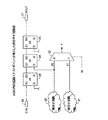
図7はASIC内の回路にテストポイントを挿入した例を示す回路図である。図7中、20、21は論理設計された組合せ回路、22は選択制御信号としてテストモード信号Xtが与えられるセレクタであり、選択制御信号Xtは、テストモード時には“1”とされる。本例では、セレクタ22は、テストモード信号Xt=“0”の場合には、X0端子の信号、即ち、組合せ回路20の出力信号を選択し、テストモード信号Xt=“1”の場合には、X1端子の信号、即ち、組合せ回路21の出力信号を選択する。
FIG. 7 is a circuit diagram showing an example in which test points are inserted into circuits in the ASIC. In FIG. 7, 20 and 21 are logically designed combinational circuits, 22 is a selector to which a test mode signal Xt is given as a selection control signal, and the selection control signal Xt is set to “1” in the test mode. In this example, when the test mode signal Xt = “0”, the
また、23〜25はスキャンテスト用のフリップフロップ、26はSIN端子、27はSOUT端子であり、フリップフロップ24は、セレクタ22のX0端子の信号(組合せ回路20の出力信号)を観測するためにテストポイントとして挿入されたフリップフロップである。
図7に示す回路においては、テストモード信号Xt=“1”とされるテストモード時には、組合せ回路21の出力信号のみがセレクタ22のY端子に出力され、組合せ回路20の出力信号はセレクタ22のY端子には出力されない。このため、組合せ回路20の出力信号が異常であっても、その故障を検出することができないことになり、故障検出率の低下を招くことになる。
In the circuit shown in FIG. 7, in the test mode where the test mode signal Xt = “1”, only the output signal of the
そこで、このような場合には、スキャンチェーンの一部をなすテストポイント24を挿入し、セレクタ22のX0端子をテストポイント24のD端子に接続する。このようにすると、スキャンテスト時にセレクタ22のX0端子の信号を観測することができ、これにより、組合せ回路20の出力信号の故障検出を行うことができ、故障検出率を高めることができる。
従来、設計対象のASIC内の回路にテストポイントを挿入する場合、テストパターンを用いてコンピュータ上でシミュレーションを行い、テストパターンにより故障を検出することができなかった箇所をリストに出力し、このリストを元に、作業者が回路を目視で確認しながら、テストポイントの挿入位置を決めるという方法が採られていた。このテストポイント挿入方法は、回路を目視する必要があるため、非省力的であり、かつ、テストポイント挿入箇所の選定は作業者の主観によるものであるため、作業者の技量により故障検出の効果が左右されるという問題点を有していた。 Conventionally, when a test point is inserted into a circuit in an ASIC to be designed, a simulation is performed on a computer using a test pattern, and a place where a failure cannot be detected by the test pattern is output to a list. Based on the above, a method has been adopted in which an operator determines the test point insertion position while visually checking the circuit. This test point insertion method is labor-saving because it is necessary to visually observe the circuit, and the selection of the test point insertion point is based on the subjectivity of the operator. Has the problem of being affected.
本発明は、かかる点に鑑み、半導体集積回路のテスト設計時におけるテストポイントの挿入を省力的かつ効果的に行い、故障検出率の向上を図ることができるテストポイント自動挿入方法及びプログラムを提供することを目的とする。 In view of the above, the present invention provides a test point automatic insertion method and program capable of labor-saving and effective test point insertion at the time of test design of a semiconductor integrated circuit and improving the failure detection rate. For the purpose.
本発明のテストポイント自動挿入方法は、コンピュータを使用し、半導体集積回路のテスト設計時に、該半導体集積回路内の回路にテストポイントを自動挿入する方法であって、前記回路について、テストモード信号の論理値を固定しない場合の第1の2分決定グラフと、前記テストモード信号の論理値をテストモード時の値に固定した場合の第2の2分決定グラフを作成する工程と、前記第1、第2の2分決定グラフを比較し、前記第1、第2の2分決定グラフが一致しない場合には、前記第2の2分決定グラフには無いノードを検出し、選択制御信号として前記テストモード信号が与えられるセレクタの入力端子のうち、前記テストモード信号の論理値をテストモード時の値に固定した場合に伝播されなくなる信号が与えられる入力端子を探索し、該探索した入力端子の信号を観測するためのテストポイントを挿入する工程を有するものである。 The test point automatic insertion method of the present invention is a method of automatically inserting test points into a circuit in a semiconductor integrated circuit at the time of test design of the semiconductor integrated circuit using a computer, Creating a first binary decision graph when the logic value is not fixed, a second binary decision graph when the logic value of the test mode signal is fixed to a value in the test mode, and the first The second binary decision graphs are compared, and if the first and second binary decision graphs do not match, a node that is not in the second binary decision graph is detected and used as a selection control signal. Among the input terminals of the selector to which the test mode signal is applied, the input terminal to which a signal that is not propagated when the logic value of the test mode signal is fixed to the value in the test mode is applied I searched, and has a step of inserting a test point for observing the signal of the input terminal and the search.
本発明のテストポイント自動挿入プログラムは、半導体集積回路のテスト設計時に、該半導体集積回路内の回路にテストポイントを自動挿入する工程をコンピュータに実行させるプログラムであって、前記回路について、テストモード信号の論理値を固定しない場合の第1の2分決定グラフと、前記テストモード信号の論理値をテストモード時の値に固定した場合の第2の2分決定グラフを作成する工程と、前記第1、第2の2分決定グラフを比較し、前記第1、第2の2分決定グラフが一致しない場合には、前記第2の2分決定グラフには無いノードを検出し、選択制御信号として前記テストモード信号が与えられるセレクタの入力端子のうち、前記テストモード信号の論理値をテストモード時の値に固定した場合に伝播されなくなる信号が与えられる入力端子を探索し、該探索した入力端子の信号を観測するためのテストポイントを挿入する工程をコンピュータに実行させるものである。 The test point automatic insertion program of the present invention is a program for causing a computer to execute a process of automatically inserting a test point into a circuit in the semiconductor integrated circuit at the time of test design of the semiconductor integrated circuit. Generating a first binary decision graph when the logic value of the test mode signal is not fixed, a second binary decision graph when the logic value of the test mode signal is fixed to the value at the time of the test mode, The first and second binary decision graphs are compared, and if the first and second binary decision graphs do not match, a node that is not in the second binary decision graph is detected, and the selection control signal Among the input terminals of the selector to which the test mode signal is given, a signal that is not propagated when the logic value of the test mode signal is fixed to the value in the test mode Explore the input terminals provided, it is intended to execute the step of inserting a test point for observing the signal of the input terminal and the search to a computer.
また、本発明のテストポイント自動挿入方法及びプログラムにおいては、前記テストポイントを挿入する工程は、前記第2の2分決定グラフには無いノードに対応する前記回路内のノードから前記探索した入力端子までのセル端子数が予め設定された値以上であるか否かを判断する工程を含み、前記セル端子数が前記予め設定された値以上の場合に、前記テストポイントを挿入するとしても良い。 Also, in the test point automatic insertion method and program of the present invention, the step of inserting the test point is the input terminal searched for from a node in the circuit corresponding to a node not in the second binary decision graph. A step of determining whether or not the number of cell terminals is equal to or greater than a preset value, and the test point may be inserted when the number of cell terminals is equal to or greater than the preset value.
本発明よれば、コンピュータにより、テストモード信号の論理値を固定しない場合の第1の2分決定グラフと、テストモード信号の論理値をテストモード時の値に固定した場合の第2の2分決定グラフを作成し、これら第1、第2の2分決定グラフを比較し、第1、第2の2分決定グラフが一致しない場合には、第2の2分決定グラフには無いノードを検出し、選択制御信号としてテストモード信号が与えられるセレクタの入力端子のうち、テストモード信号の論理値をテストモード時の値に固定した場合に伝播されなくなる信号が与えられる入力端子を探索し、該探索した入力端子の信号を観測するためのテストポイントを挿入することができる。 According to the present invention, the first binary decision graph when the logical value of the test mode signal is not fixed by the computer and the second binary decision when the logical value of the test mode signal is fixed to the value in the test mode. Create a decision graph, compare these first and second binary decision graphs, and if the first and second binary decision graphs do not match, select a node that is not in the second binary decision graph Detecting and searching for an input terminal to which a signal that is not propagated when the logic value of the test mode signal is fixed to the value at the time of the test mode among the input terminals of the selector to which the test mode signal is given as a selection control signal, A test point for observing the signal of the searched input terminal can be inserted.
したがって、従来のように、テストパターンを用いてコンピュータ上でシミュレーションを行い、テストパターンにより故障を検出することができなかった箇所をリストに出力し、このリストを元に、作業者が回路を目視で確認しながら、テストポイントの挿入位置を決めるという工程を必要としない。即ち、本発明によれば、テストポイントを必要な箇所に自動的に挿入することができるので、半導体集積回路のテスト設計時におけるテストポイントの挿入を省力的かつ効果的に行い、故障検出率の向上を図ることができる。 Therefore, a simulation is performed on a computer using a test pattern as in the past, and a location where a failure could not be detected by the test pattern is output to a list. Based on this list, an operator visually checks the circuit. The process of determining the insertion point of the test point is not required while confirming with. That is, according to the present invention, since test points can be automatically inserted at necessary places, the test points are inserted labor-saving and effectively at the time of test design of a semiconductor integrated circuit. Improvements can be made.
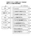
図1は本発明のテストポイント自動挿入方法の一実施形態を実施するための装置の概略的構成図である。この装置はコンピュータからなり、CPU(中央制御装置)30、半導体メモリ31、マウス32、キーボード33、ディスプレイ34及びハードディスク35等を備えており、ハードディスク35には、本発明のテストポイント自動挿入方法の一実施形態の実施に必要なデータ及びプログラム(本発明のテストポイント自動挿入プログラムの一実施形態)等が格納される。
FIG. 1 is a schematic configuration diagram of an apparatus for carrying out an embodiment of a test point automatic insertion method of the present invention. This apparatus is composed of a computer and includes a CPU (Central Control Unit) 30, a
本例の場合、データとしては、設計対象のASICのネットリスト36が使用され、プログラムとしては、2分決定グラフ作成プログラム37、2分決定グラフ比較プログラム38、ノード検出プログラム39、セレクタ入力端子探索プログラム40、セル端子数判断プログラム41及びテストポイント挿入プログラム42が使用される。
In this example, the
2分決定グラフ作成プログラム37は、設計対象のASICのネットリスト36から2分決定グラフを作成するプログラムであり、本例では、テストモード信号の論理値を固定しない場合の第1の2分決定グラフと、テストモード信号の論理値をテストモード時の値に固定した場合の第2の2分決定グラフが作成される。
The binary decision
2分決定グラフ比較プログラム38は、第1の2分決定グラフと第2の2分決定グラフが一致するか否かを比較するプログラムである。ノード検出プログラム39は、第1の2分決定グラフにはあるが、第2の2分決定グラフには無いノード、即ち、第1の2分決定グラフ内のノードからテストモード信号によりマスクされたノードを検出するプログラムである。
The binary decision
セレクタ入力端子探索プログラム40は、第2の2分決定グラフには無いノードに対応するASICの回路内のノード上の信号、即ち、テストモード信号によりマスクされた信号が入力される組合せ回路の接続を解析し、選択制御信号としてテストモード信号が与えられるセレクタの入力端子のうち、テストモード信号によりマスクされた信号が入力される組合せ回路の出力信号が与えられる入力端子を探索するプログラムである。
The selector input
セル端子数判断プログラム41は、第2の2分決定グラフには無いノードに対応するASICの回路内のノードから、選択制御信号としてテストモード信号が与えられるセレクタの入力端子までのセル端子数が設計者又はユーザにより予め設定された値以上であるか否かを判断するプログラムである。テストポイント挿入プログラム42は、テストモード信号によりマスクされた信号が入力される組合せ回路の出力信号を観測するためのテストポイントを挿入するプログラムである。
The cell terminal
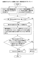
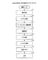
図2は本発明のテストポイント自動挿入方法の一実施形態を示すフローチャートである。即ち、本発明のテストポイント自動挿入方法の一実施形態を実施する場合には、まず、設計対象のASICのネットリスト36及び2分決定グラフ作成プログラム37を使用して、テストモード信号の論理値を固定しない場合の第1の2分決定グラフ43を作成し、作成した第1の2分決定グラフ43をハードディスク35に格納する(ステップP1)。
FIG. 2 is a flowchart showing an embodiment of the test point automatic insertion method of the present invention. That is, when one embodiment of the test point automatic insertion method of the present invention is implemented, first, the logic value of the test mode signal is calculated by using the
また、設計対象のASICのネットリスト36及び2分決定グラフ作成プログラム37を使用して、テストモード信号の論理値をテストモード時の値に固定した場合の第2の2分決定グラフ44を作成し、作成した第2の2分決定グラフ44をハードディスク35に格納する(ステップP2)。
Also, a second
次に、2分決定グラフ比較プログラム38を使用して、第1の2分決定グラフ43と第2の2分決定グラフ44が一致しているか否かを比較する(ステップP3)。比較の結果、第1の2分決定グラフ43と第2の2分決定グラフ44が一致している場合には、テストポイントを挿入せず、テストポイント自動挿入処理を終了する。
Next, the binary decision
これに対して、第1の2分決定グラフ43と第2の2分決定グラフ44が一致しない場合には、設計対象のASICの回路内にテストモード信号によりマスクされる信号が存在するので、ノード検出プログラム39を使用して、第1の2分決定グラフ43にはあるが、第2の2分決定グラフ44には無いノードを検出する(ステップP4)。なお、第2の2分決定グラフ44に無いノードに対応するASICの回路内のノード上の信号がテストモード信号によりマスクされる信号ということになる。
On the other hand, when the first
次に、セレクタ入力端子探索プログラム40を使用して、第2の2分決定グラフ44に無いノードに対応するASICの回路内のノード上の信号、即ち、テストモード信号によりマスクされた信号が入力される組合せ回路の接続を解析し、選択制御信号としてテストモード信号が与えられるセレクタの入力端子のうち、テストモード信号によりマスクされた信号が入力される組合せ回路の出力信号が与えられる入力端子を探索する(ステップP5)。いわば、テストモード信号と、テストモード信号によりマスクされた信号が入力される組合せ回路の出力信号との交点を探索する。
Next, the selector input
次に、第2の2分決定グラフ44には無いノードに対応するASICの回路内のノードからステップP5で探索したセレクタの入力端子までのセル端子数が設計者又はユーザにより予め設定された値以上であるか否かを判断する(ステップP6)。第2の2分決定グラフ44には無いノードに対応するASICの回路内のノードからステップP5で探索したセレクタの入力端子までのセル端子数を予め設定するのは、テストポイントを挿入しても故障検出に効果が少ない場合に、不要にテストポイントを入れないようにするためである。
Next, the number of cell terminals from the node in the ASIC circuit corresponding to the node not included in the second
ステップP6における判断の結果、第2の2分決定グラフ44には無いノードに対応するASICの回路内のノードからステップP5で探索したセレクタの入力端子までのセル端子数が予め設定された値以上でない場合には、テストポイントを挿入せず、テストポイント自動挿入処理を終了する。
As a result of the determination in step P6, the number of cell terminals from the node in the ASIC circuit corresponding to the node not in the second
これに対して、第2の2分決定グラフ44には無いノードに対応するASICの回路内のノードからステップP5で探索したセレクタの入力端子までのセル端子数が予め設定された値以上である場合には、ステップP5で探索したセレクタの入力端子の信号を観測するためのテストポイントを挿入する(ステップP7)。以上のステップP1〜P7をASIC内の全回路に対して行う。
In contrast, the number of cell terminals from a node in the ASIC circuit corresponding to a node not included in the second
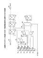
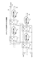
図3は本発明のテストポイント自動挿入方法の一実施形態を具体的に説明するための回路図であり、設計対象のASICの一部分を示している。図3中、50〜55はフリップフロップ、X1〜X6はフリップフロップ50〜55が出力する信号、56は信号X1〜X4を入力信号とする組合せ回路であり、57は信号X1〜X3をAND処理するAND回路、58はAND回路57の出力と信号X4をOR処理するOR回路、59は信号X5、X6をAND処理するAND回路である。
FIG. 3 is a circuit diagram for specifically explaining an embodiment of the test point automatic insertion method of the present invention, and shows a part of an ASIC to be designed. In FIG. 3, 50 to 55 are flip-flops, X1 to X6 are signals output from the flip-
また、60はテストモード信号Xtにより選択動作が制御され、組合せ回路56の出力信号又はAND回路59の出力信号を選択するセレクタであり、このセレクタ60は、テストモード信号Xt=“0”の場合は、OR回路58の出力を選択し、テストモード信号Xt=“1”の場合は、AND回路59の出力を選択する。61はセレクタ60の出力信号を取り込むフリップフロップ、62〜64はスキャンチェーンを構成するフリップフロップであり、フリップフロップ63は、テストポイントである。65はSIN端子、66はSOUT端子である。
なお、本発明のテストポイント自動挿入方法の一実施形態においては、入力信号と出力信号の関係は、外部端子間だけでなく、フリップフロップとフリップフロップとの間、フリップフロップとラッチ回路との間、ラッチ回路とフリップフロップとの間、フリップフロップとグローバル・クロック・バッファとの間など、順序回路と順序回路との間で区切ることができる。2分決定グラフを作成する場合も、この区切りで作成される。 In one embodiment of the test point automatic insertion method of the present invention, the relationship between the input signal and the output signal is not only between the external terminals, but also between the flip-flop and the flip-flop, and between the flip-flop and the latch circuit. , Between the sequential circuit and the sequential circuit, such as between the latch circuit and the flip-flop, and between the flip-flop and the global clock buffer. When creating a binary decision graph, it is also created at this break.
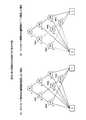
ここで、図3に示す回路に本発明のテストポイント自動挿入方法の一実施形態を適用すると、まず、図3に示す回路について、テストモード信号Xtの論理値を固定しない場合の第1の2分決定グラフが作成されるが(ステップP1)、この場合に作成される第1の2分決定グラフは、図4(A)に示すようになる。なお、2分決定グラフを作成する場合には、テストモード信号Xtを始点として作成する。 Here, when one embodiment of the test point automatic insertion method of the present invention is applied to the circuit shown in FIG. 3, first, in the circuit shown in FIG. 3, the first 2 in the case where the logic value of the test mode signal Xt is not fixed. A minute determination graph is created (step P1). The first binary decision graph created in this case is as shown in FIG. When creating a binary decision graph, the test mode signal Xt is used as a starting point.
次に、テストモード信号Xtの論理値をテストモード時の値である“1”に固定した場合の第2の2分決定グラフが作成されるが(ステップP2)、この場合に作成される第2の2分決定グラフは、図4(B)に示すようになる。なお、この場合の2分決定グラフは、破線で示すパスが存在しない状態になっている。 Next, a second binary decision graph is created when the logic value of the test mode signal Xt is fixed to “1” which is the value in the test mode (step P2). In this case, the second binary decision graph is created. The binary decision graph of 2 is as shown in FIG. In this case, the binary decision graph is in a state where there is no path indicated by a broken line.
次に、図4(A)に示す第1の2分決定グラフと図4(B)に示す第2の2分決定グラフが一致しているか否かが比較されるが(ステップP3)、図4(B)に示す第2の2分決定グラフにおける破線のパスが差分として存在することになる。この比較の結果、ノードNA1〜NA4が第2の2分決定グラフに無いノードであり、図3に示す信号X1〜X4がテストモード信号Xtによりマスクされており、故障検出ができなくなっている信号であるということになる。 Next, it is compared whether or not the first binary decision graph shown in FIG. 4A matches the second binary decision graph shown in FIG. 4B (step P3). A broken-line path in the second binary decision graph shown in 4 (B) exists as a difference. As a result of the comparison, the nodes NA1 to NA4 are nodes that are not in the second binary decision graph, and the signals X1 to X4 shown in FIG. 3 are masked by the test mode signal Xt, so that the failure detection cannot be performed. It means that.
次に、テストモード信号Xtによりマスクされた信号X1〜X4が入力される組合せ回路56の接続が解析され、セレクタ60の入力端子のうち、組合せ回路56の出力信号が与えられる入力端子が探索されるが(ステップP5)、この場合、入力端子Q6が探索され、入力端子Q6がテストポイントのD端子を接続する候補となる。
Next, the connection of the
次に、図4(B)に示す第2の2分決定グラフには無いノードNA1〜NA4に対応するASICの回路内のノードNB1〜NB4からステップP5で探索したセレクタ60の入力端子Q6までの組合せ回路56内のセル端子数が予め設定された値以上であるか否かが判断されるが(ステップP6)、本例では、組合せ回路56内のセル端子は、Q1〜Q5であり、組合せ回路56内のセル端子数は5である。
Next, from the nodes NB1 to NB4 in the ASIC circuit corresponding to the nodes NA1 to NA4 which are not included in the second binary decision graph shown in FIG. 4B to the input terminal Q6 of the
したがって、セル端子数=5が予め設定された値未満の場合には、テストポイントを挿入しないで、テストポイント自動挿入処理を終了し、セル端子数=5が予め設定された値以上の場合には、テストポイント63を挿入し、テストポイント63のD端子を入力端子Q6に接続して処理を終了する。
Therefore, when the number of cell terminals = 5 is less than a preset value, the test point automatic insertion process is terminated without inserting a test point, and when the number of cell terminals = 5 is equal to or more than a preset value. Inserts the
以上のように、本発明のテストポイント自動挿入方法の一実施形態においては、図1に示すコンピュータからなる装置と、設計対象のASICのネットリスト36及び本発明のテストポイント自動挿入プログラムの一実施形態を構成するプログラム(2分決定グラフ作成プログラム37、2分決定グラフ比較プログラム38、ノード検出プログラム39、セレクタ入力端子探索プログラム40、セル端子数判断プログラム41及びテストポイント挿入プログラム42)が使用される。
As described above, in one embodiment of the automatic test point insertion method of the present invention, the apparatus comprising the computer shown in FIG. 1, the ASIC netlist 36 to be designed, and the test point automatic insertion program of the present invention are implemented. The program (the binary decision
そして、テストモード信号の論理値を固定しない場合の第1の2分決定グラフと、テストモード信号の論理値をテストモード時の値に固定した場合の第2の2分決定グラフを作成し、これら第1、第2の2分決定グラフを比較し、第1、第2の2分決定グラフが一致しない場合には、第2の2分決定グラフには無いノードを検出し、選択制御信号としてテストモード信号が与えられるセレクタの入力端子のうち、テストモード信号の論理値をテストモード時の値に固定した場合にマスクされた信号が入力される組合せ回路の出力信号が与えられる入力端子を探索し、該探索した入力端子の信号を観測するテストポイントを挿入するとしている。 Then, a first binary decision graph when the logic value of the test mode signal is not fixed and a second binary decision graph when the logic value of the test mode signal is fixed to the value in the test mode are created, These first and second binary decision graphs are compared, and if the first and second binary decision graphs do not match, a node not in the second binary decision graph is detected, and the selection control signal Among the input terminals of the selector to which the test mode signal is given, the input terminal to which the output signal of the combinational circuit to which the masked signal is inputted when the logic value of the test mode signal is fixed to the value in the test mode is given It is assumed that a test point for searching and observing the signal of the searched input terminal is inserted.
したがって、従来のように、テストパターンを用いてコンピュータ上でシミュレーションを行い、テストパターンにより故障を検出することができなかった箇所をリストに出力し、このリストを元に、作業者が回路を目視で確認しながら、テストポイントの挿入位置を決めるという工程を必要としない。即ち、本発明のテストポイント自動挿入方法の一実施形態によれば、テストポイントを必要な箇所に自動的に挿入することができるので、半導体集積回路のテスト設計時におけるテストポイントの挿入を省力的かつ効果的に行い、故障検出率の向上を図ることができる。 Therefore, a simulation is performed on a computer using a test pattern as in the past, and a location where a failure could not be detected by the test pattern is output to a list. Based on this list, an operator visually checks the circuit. The process of determining the insertion point of the test point is not required while confirming with. That is, according to one embodiment of the test point automatic insertion method of the present invention, test points can be automatically inserted at a necessary place, so that test point insertion at the time of test design of a semiconductor integrated circuit is labor-saving. It is possible to effectively and effectively improve the failure detection rate.
ここで、本発明を整理すると、本発明には、少なくとも、以下のテストポイント自動挿入方法及びプログラムが含まれる。 Here, when the present invention is arranged, the present invention includes at least the following test point automatic insertion method and program.
(付記1)コンピュータを使用し、半導体集積回路のテスト設計時に、該半導体集積回路内の回路にテストポイントを自動挿入するテストポイント自動挿入方法であって、前記回路について、テストモード信号の論理値を固定しない場合の第1の2分決定グラフと、前記テストモード信号の論理値をテストモード時の値に固定した場合の第2の2分決定グラフを作成する工程と、前記第1、第2の2分決定グラフを比較し、前記第1、第2の2分決定グラフが一致しない場合には、前記第2の2分決定グラフには無いノードを検出し、選択制御信号として前記テストモード信号が与えられるセレクタの入力端子のうち、前記テストモード信号の論理値をテストモード時の値に固定した場合に伝播されなくなる信号が与えられる入力端子を探索し、該探索した入力端子の信号を観測するためのテストポイントを挿入する工程を有することを特徴とするテストポイント自動挿入方法。 (Supplementary note 1) A test point automatic insertion method for automatically inserting a test point into a circuit in a semiconductor integrated circuit at the time of test design of the semiconductor integrated circuit using a computer, wherein the logic value of the test mode signal for the circuit Generating a first binary decision graph when the test mode signal is fixed, and a second binary decision graph when the logic value of the test mode signal is fixed to the value in the test mode; 2 binary decision graphs are compared, and if the first and second binary decision graphs do not match, a node that is not in the second binary decision graph is detected, and the test is performed as a selection control signal. Among the input terminals of the selector to which the mode signal is given, the input terminal to which the signal that is not propagated when the logic value of the test mode signal is fixed to the value in the test mode is given is searched. , Test points automatic insertion method characterized in that it comprises a step of inserting a test point for observing the signal of the input terminal and the search.
(付記2)前記テストポイントを挿入する工程は、前記第2の2分決定グラフには無いノードに対応する前記回路内のノードから前記探索した入力端子までのセル端子数が予め設定された値以上であるか否かを判断する工程を含み、前記セル端子数が前記予め設定された値以上の場合に、前記テストポイントを挿入することを特徴とする付記1記載のテストポイント自動挿入方法。
(Supplementary Note 2) The step of inserting the test point is a value in which the number of cell terminals from a node in the circuit corresponding to a node not in the second binary decision graph to the searched input terminal is set in advance. The test point automatic insertion method according to
(付記3)前記回路は、順序回路で区切られた回路であることを特徴とする付記1又は2記載のテストポイント自動挿入方法。
(Supplementary note 3) The test point automatic insertion method according to
(付記4)半導体集積回路のテスト設計時に、該半導体集積回路内の回路にテストポイントを自動挿入する工程をコンピュータに実行させるテストポイント自動挿入プログラムであって、前記回路について、テストモード信号の論理値を固定しない場合の第1の2分決定グラフと、前記テストモード信号の論理値をテストモード時の値に固定した場合の第2の2分決定グラフを作成する工程と、前記第1、第2の2分決定グラフを比較し、前記第1、第2の2分決定グラフが一致しない場合には、前記第2の2分決定グラフには無いノードを検出し、選択制御信号として前記テストモード信号が与えられるセレクタの入力端子のうち、前記テストモード信号の論理値をテストモード時の値に固定した場合に伝播されなくなる信号が与えられる入力端子を探索し、該探索した入力端子の信号を観測するためのテストポイントを挿入する工程をコンピュータに実行させることを特徴とするテストポイント自動挿入プログラム。 (Supplementary Note 4) A test point automatic insertion program for causing a computer to execute a process of automatically inserting a test point into a circuit in the semiconductor integrated circuit at the time of test design of the semiconductor integrated circuit. Creating a first binary decision graph when the value is not fixed, and a second binary decision graph when the logic value of the test mode signal is fixed to the value in the test mode; When the second binary decision graphs are compared and the first and second binary decision graphs do not match, a node that is not in the second binary decision graph is detected, and the selection control signal is used as the selection control signal. Among the input terminals of the selector to which the test mode signal is given, a signal that is not propagated when the logic value of the test mode signal is fixed to the value in the test mode is given Searching a force terminal, test points automatic insertion program characterized by executing the step of inserting a test point for observing the signal of the input terminal and the search to a computer.
(付記5)前記テストポイントを挿入する工程は、前記第2の2分決定グラフには無いノードに対応する前記回路内のノードから前記探索した入力端子までのセル端子数が予め設定された値以上であるか否かを判断する工程を含み、前記セル端子数が前記予め設定された値以上の場合に、前記テストポイントを挿入することを特徴とする付記4記載のテストポイント自動挿入プログラム。 (Supplementary Note 5) The step of inserting the test point is a value in which the number of cell terminals from a node in the circuit corresponding to a node not in the second binary decision graph to the searched input terminal is set in advance. The program for automatically inserting test points according to appendix 4, wherein a test point is inserted when the number of cell terminals is equal to or greater than the preset value, including a step of determining whether or not the above is true.
(付記6)前記回路は、順序回路で区切られた回路であることを特徴とする付記4又は5記載のテストポイント自動挿入プログラム。 (Supplementary note 6) The test point automatic insertion program according to supplementary note 4 or 5, wherein the circuit is a circuit divided by a sequential circuit.
1〜4…組合せ回路
5〜8…フリップフロップ
9…SIN(スキャンイン)端子
10…SOUT(スキャンアウト)端子
11…CLK(クロック)端子
20、21…組合せ回路
22…セレクタ
23〜25…フリップフロップ
26…SIN端子
27…SOUT端子
30…CPU
31…半導体メモリ
32…マウス
33…キーボード
34…ディスプレイ
35…ハードディスク
36…ネットリスト
37…2分決定グラフ作成プログラム
38…2分決定グラフ比較プログラム
39…ノード検出プログラム
40…セレクタ入力端子探索プログラム
41…セル端子数判断プログラム
42…テストポイント挿入プログラム
43…第1の2分決定グラフ
44…第2の2分決定グラフ
50〜55…フリップフロップ
56…組合せ回路
57…AND回路
58…OR回路
59…AND回路
60…セレクタ
61〜64…フリップフロップ
65…SIN端子
66…SOUT端子
DESCRIPTION OF SYMBOLS 1-4 ... Combination circuit 5-8 ... Flip flop 9 ... SIN (scan in) terminal 10 ... SOUT (scan out) terminal 11 ... CLK (clock)
DESCRIPTION OF
Claims (5)
前記回路について、テストモード信号の論理値を固定しない場合の第1の2分決定グラフと、前記テストモード信号の論理値をテストモード時の値に固定した場合の第2の2分決定グラフを作成する工程と、
前記第1、第2の2分決定グラフを比較し、前記第1、第2の2分決定グラフが一致しない場合には、前記第2の2分決定グラフには無いノードを検出し、選択制御信号として前記テストモード信号が与えられるセレクタの入力端子のうち、前記テストモード信号の論理値をテストモード時の値に固定した場合に伝播されなくなる信号が与えられる入力端子を探索し、該探索した入力端子の信号を観測するためのテストポイントを挿入する工程を有することを特徴とするテストポイント自動挿入方法。 A test point automatic insertion method for automatically inserting a test point into a circuit in a semiconductor integrated circuit at the time of test design of the semiconductor integrated circuit using a computer,
For the circuit, a first binary decision graph when the logic value of the test mode signal is not fixed, and a second binary decision graph when the logic value of the test mode signal is fixed to the value in the test mode. Creating a process;
Compare the first and second binary decision graphs, and if the first and second binary decision graphs do not match, detect and select a node not in the second binary decision graph Search among input terminals of a selector to which the test mode signal is given as a control signal, for an input terminal to which a signal that is not propagated when the logic value of the test mode signal is fixed to the value in the test mode is given. A test point automatic insertion method comprising a step of inserting a test point for observing a signal at the input terminal.
前記回路について、テストモード信号の論理値を固定しない場合の第1の2分決定グラフと、前記テストモード信号の論理値をテストモード時の値に固定した場合の第2の2分決定グラフを作成する工程と、
前記第1、第2の2分決定グラフを比較し、前記第1、第2の2分決定グラフが一致しない場合には、前記第2の2分決定グラフには無いノードを検出し、選択制御信号として前記テストモード信号が与えられるセレクタの入力端子のうち、前記テストモード信号の論理値をテストモード時の値に固定した場合に伝播されなくなる信号が与えられる入力端子を探索し、該探索した入力端子の信号を観測するためのテストポイントを挿入する工程をコンピュータに実行させることを特徴とするテストポイント自動挿入プログラム。 A test point automatic insertion program for causing a computer to execute a process of automatically inserting a test point into a circuit in the semiconductor integrated circuit at the time of test design of the semiconductor integrated circuit,
For the circuit, a first binary decision graph when the logic value of the test mode signal is not fixed, and a second binary decision graph when the logic value of the test mode signal is fixed to the value in the test mode. Creating a process;
Compare the first and second binary decision graphs, and if the first and second binary decision graphs do not match, detect and select a node not in the second binary decision graph Search among input terminals of a selector to which the test mode signal is given as a control signal, for an input terminal to which a signal that is not propagated when the logic value of the test mode signal is fixed to the value in the test mode is given. An automatic test point insertion program for causing a computer to execute a step of inserting a test point for observing a signal at an input terminal.
5. The test point automatic insertion program according to claim 3, wherein the circuit is a circuit divided by a sequential circuit.
Priority Applications (1)
| Application Number | Priority Date | Filing Date | Title |
|---|---|---|---|
| JP2006181065A JP2008009827A (en) | 2006-06-30 | 2006-06-30 | Test point automatic insertion method and program |
Applications Claiming Priority (1)
| Application Number | Priority Date | Filing Date | Title |
|---|---|---|---|
| JP2006181065A JP2008009827A (en) | 2006-06-30 | 2006-06-30 | Test point automatic insertion method and program |
Publications (1)
| Publication Number | Publication Date |
|---|---|
| JP2008009827A true JP2008009827A (en) | 2008-01-17 |
Family
ID=39067956
Family Applications (1)
| Application Number | Title | Priority Date | Filing Date |
|---|---|---|---|
| JP2006181065A Withdrawn JP2008009827A (en) | 2006-06-30 | 2006-06-30 | Test point automatic insertion method and program |
Country Status (1)
| Country | Link |
|---|---|
| JP (1) | JP2008009827A (en) |
-
2006
- 2006-06-30 JP JP2006181065A patent/JP2008009827A/en not_active Withdrawn
Similar Documents
| Publication | Publication Date | Title |
|---|---|---|
| US8543966B2 (en) | Test path selection and test program generation for performance testing integrated circuit chips | |
| US10691855B2 (en) | Device and method for detecting points of failures | |
| US7562321B2 (en) | Method and apparatus for structured ASIC test point insertion | |
| US7082558B2 (en) | Increasing possible test patterns which can be used with sequential scanning techniques to perform speed analysis | |
| JP6731733B2 (en) | Scan test circuit, scan test method, and scan test circuit design method | |
| US10977400B2 (en) | Deterministic test pattern generation for designs with timing exceptions | |
| US12423491B2 (en) | Identifying association of safety related ports to their safety mechanisms through structural analysis | |
| JP5567322B2 (en) | Test flow presentation computer program, test flow presentation computer system | |
| Chakraborty et al. | Effective path selection for delay fault testing of sequential circuits | |
| JPH0989980A (en) | Semiconductor integrated circuit and its evaluation method | |
| US6876934B2 (en) | Method for determining fault coverage from RTL description | |
| US20100131910A1 (en) | Simulating Scan Tests with Reduced Resources | |
| JP2008009827A (en) | Test point automatic insertion method and program | |
| US12474396B2 (en) | Test logic method for an integrated circuit device | |
| JP3829021B2 (en) | Easier test design rule inspection device | |
| US10234504B1 (en) | Optimizing core wrappers in an integrated circuit | |
| Lin et al. | Speed binning with high-quality structural patterns from functional timing analysis (FTA) | |
| JP4020731B2 (en) | Fault diagnosis method for semiconductor integrated circuit | |
| US20260002991A1 (en) | Test pattern generating method and device | |
| CN118966108B (en) | Analysis method, analysis device, electronic device, storage medium, and program product for circuit controllability | |
| JP4028574B2 (en) | LSI testability design method | |
| Sun et al. | On the generation of diagnostic test set for intra-cell defects | |
| JP2011060117A (en) | Support device for semiconductor integrated circuit design and design method of semiconductor integrated circuit | |
| JP2013015494A (en) | Semiconductor integrated circuit and inspection method of semiconductor integrated circuit | |
| JP2007226818A (en) | LSI testability design method |
Legal Events
| Date | Code | Title | Description |
|---|---|---|---|
| A711 | Notification of change in applicant |
Free format text: JAPANESE INTERMEDIATE CODE: A712 Effective date: 20080730 |
|
| A621 | Written request for application examination |
Free format text: JAPANESE INTERMEDIATE CODE: A621 Effective date: 20090302 |
|
| A761 | Written withdrawal of application |
Free format text: JAPANESE INTERMEDIATE CODE: A761 Effective date: 20101126 |