JP2008009801A - Method for producing rfid inlet - Google Patents
Method for producing rfid inlet Download PDFInfo
- Publication number
- JP2008009801A JP2008009801A JP2006180703A JP2006180703A JP2008009801A JP 2008009801 A JP2008009801 A JP 2008009801A JP 2006180703 A JP2006180703 A JP 2006180703A JP 2006180703 A JP2006180703 A JP 2006180703A JP 2008009801 A JP2008009801 A JP 2008009801A
- Authority
- JP
- Japan
- Prior art keywords
- antenna
- foil
- rfid inlet
- rfid
- manufacturing
- Prior art date
- Legal status (The legal status is an assumption and is not a legal conclusion. Google has not performed a legal analysis and makes no representation as to the accuracy of the status listed.)
- Pending
Links
- 238000004519 manufacturing process Methods 0.000 title claims abstract description 39
- 239000011888 foil Substances 0.000 claims abstract description 78
- 239000004065 semiconductor Substances 0.000 claims description 48
- 238000005520 cutting process Methods 0.000 claims description 40
- 239000004020 conductor Substances 0.000 claims description 23
- 238000000034 method Methods 0.000 claims description 17
- 238000004080 punching Methods 0.000 claims description 13
- 230000015572 biosynthetic process Effects 0.000 claims description 9
- 230000008569 process Effects 0.000 claims description 6
- 229910052782 aluminium Inorganic materials 0.000 claims description 3
- XAGFODPZIPBFFR-UHFFFAOYSA-N aluminium Chemical compound [Al] XAGFODPZIPBFFR-UHFFFAOYSA-N 0.000 claims description 3
- 238000007789 sealing Methods 0.000 claims description 2
- 238000004891 communication Methods 0.000 abstract description 5
- 239000010931 gold Substances 0.000 description 38
- 239000011347 resin Substances 0.000 description 10
- 229920005989 resin Polymers 0.000 description 10
- 238000004382 potting Methods 0.000 description 7
- 239000002390 adhesive tape Substances 0.000 description 4
- 239000000463 material Substances 0.000 description 4
- 230000008901 benefit Effects 0.000 description 3
- 230000005674 electromagnetic induction Effects 0.000 description 3
- 238000005516 engineering process Methods 0.000 description 3
- 230000006870 function Effects 0.000 description 3
- 239000010949 copper Substances 0.000 description 2
- 238000010586 diagram Methods 0.000 description 2
- 238000012545 processing Methods 0.000 description 2
- RYGMFSIKBFXOCR-UHFFFAOYSA-N Copper Chemical compound [Cu] RYGMFSIKBFXOCR-UHFFFAOYSA-N 0.000 description 1
- 230000005540 biological transmission Effects 0.000 description 1
- 239000011248 coating agent Substances 0.000 description 1
- 238000000576 coating method Methods 0.000 description 1
- 229910052802 copper Inorganic materials 0.000 description 1
- 238000013461 design Methods 0.000 description 1
- 238000011161 development Methods 0.000 description 1
- 238000009826 distribution Methods 0.000 description 1
- 230000000694 effects Effects 0.000 description 1
- 238000009713 electroplating Methods 0.000 description 1
- PCHJSUWPFVWCPO-UHFFFAOYSA-N gold Chemical compound [Au] PCHJSUWPFVWCPO-UHFFFAOYSA-N 0.000 description 1
- 229910052737 gold Inorganic materials 0.000 description 1
- 238000010438 heat treatment Methods 0.000 description 1
- 239000002184 metal Substances 0.000 description 1
- 229910052751 metal Inorganic materials 0.000 description 1
- 238000012986 modification Methods 0.000 description 1
- 230000004048 modification Effects 0.000 description 1
- 229910021421 monocrystalline silicon Inorganic materials 0.000 description 1
- 230000003287 optical effect Effects 0.000 description 1
- 230000009467 reduction Effects 0.000 description 1
- 230000003252 repetitive effect Effects 0.000 description 1
Images

Abstract
Description
本発明は、RFID(Radio Frequency Identification)インレットの製造技術に関し、特に、UHF(極超短波)帯の電波を使用してデータを非接触で読み書きするRFIDインレットの製造に適用して有効な技術に関するものである。 The present invention relates to a manufacturing technology for an RFID (Radio Frequency Identification) inlet, and more particularly to a technology effective when applied to the manufacturing of an RFID inlet for reading and writing data in a non-contact manner using radio waves in the UHF (ultra-high frequency) band. It is.
RFIDとは、半導体チップを実装したアンテナを主体として構成されるインレットを何らかの外装に組み込んだRFIDタグを物品に取り付けておき、このRFIDタグとリーダライタ(データの読み書きのための装置)との間でデータ交換を行うことにより物品の自動認識を行う技術である。 RFID refers to an RFID tag in which an inlet composed mainly of an antenna mounted with a semiconductor chip is incorporated in an exterior, and is attached to an article. Between this RFID tag and a reader / writer (device for reading and writing data) This is a technology that automatically recognizes articles by exchanging data.
上記RFIDは、半導体チップ内のメモリ回路にデータを記憶させるため、バーコードを利用したタグなどに比べて大容量のデータを記憶できる利点がある。また、メモリ回路に記憶させたデータは、バーコードに記憶させたデータに比べて不正な改竄が困難であるという利点もある。他方、RFIDタグは、バーコードを利用したタグなどに比べてインレットの構造が複雑であることから、その製造コストが高く、これがRFIDの普及を妨げる一因となっている。 Since the RFID stores data in a memory circuit in a semiconductor chip, there is an advantage that a large amount of data can be stored as compared with a tag using a barcode. In addition, the data stored in the memory circuit has an advantage that unauthorized tampering is difficult as compared with the data stored in the barcode. On the other hand, an RFID tag has a complicated inlet structure as compared with a tag using a bar code and the like, so its manufacturing cost is high, which is one factor hindering the spread of RFID.
特許文献1(特開2005−165879号公報)は、無線タグテープ構造の一例を開示している。この無線タグテープは、所定間隔で連続して配設されたIC回路部と、このIC回路部に接続された第1アンテナ基部と、隣接して配置されたIC回路部の第1アンテナ基部を相互に電気的に接続第2アンテナ基部とを有している。無線タグテープに配設された無線タグ回路のアンテナ部は、切断前においては、隣接して配置された無線タグ回路のアンテナ部と電気的に接続されている。第1アンテナ基部は、IC回路部に接続された線状エレメントからなる。また、第2アンテナ基部は、無線タグテープの幅方向における端部に連続して形成された線状電極である。第1アンテナ基部である一対の線状エレメントのうち、少なくとも一方は、IC回路部に接続されていない側の端部において、第2アンテナ基部である線状電極に電気的に接続されている。
従来のRFIDは、2.45GHz帯のマイクロ波を使用するものや、13.56MHz帯の短波を使用する電磁誘導方式のものが一般的であった。しかし、これらのRFIDは、RFタグとリーダライタとの通信距離が短いため、適用分野が限られていた。 Conventional RFIDs generally use a 2.45 GHz band microwave and an electromagnetic induction type using a 13.56 MHz band short wave. However, these RFIDs have a limited field of application because the communication distance between the RF tag and the reader / writer is short.
最近、比較的長距離(約3メートル〜8メートル)の通信が可能で、しかも多くのタグを一度に読み取ることができるUHF帯の電波を使用するRFIDが認可されたことから、物流管理などの用途に向けた需要増大が期待されている。 Recently, RFID that uses radio waves in the UHF band, which can communicate over a relatively long distance (about 3 to 8 meters) and can read many tags at once, has been approved. Increased demand for applications is expected.
しかし、RFIDを普及させるためには、製造コスト低減が重要な課題となる。特に、UHF帯の電波を使用するRFIDインレットは、2.45GHz帯のマイクロ波や13.56MHz帯の短波を使用するRFIDインレットに比べてアンテナの寸法が大きいことから、その分、材料費が高くなってしまう。 However, in order to spread RFID, reduction of manufacturing cost is an important issue. In particular, RFID inlets that use UHF radio waves have a higher material cost because the antenna dimensions are larger than RFID inlets that use microwaves in the 2.45 GHz band and short waves in the 13.56 MHz band. turn into.
また、UHF帯の電波を使用するRFIDは、各国の利用可能な周波数帯域の中から特定の周波数が各国で割り当てており、例えば日本では950MHz、欧州では860MHz、米国では915MHzの周波数をそれぞれ割り当てている。 In addition, RFIDs that use radio waves in the UHF band are assigned specific frequencies from among the available frequency bands in each country. For example, 950 MHz in Europe, 860 MHz in Europe, and 915 MHz in the United States. Yes.
このように、UHF帯の電波を使用するRFIDは、国毎に異なる周波数の電波を使用するので、例えばA国でRFIDタグを取り付けた物品をB国に輸出した場合、A国で使用する電波の周波数とB国で使用する電波の周波数の差が大きいと、B国では通信距離が大幅に短くなったり、データの読み取りが困難になったりする。従って、UHF帯の電波を使用するRFIDでは、広い周波数帯域で効率よくデータ交換を行うことのできるインレットの開発が重要な課題となる。 In this way, since RFID using radio waves in the UHF band uses radio waves with different frequencies for each country, for example, when an article with an RFID tag attached in country A is exported to country B, the radio waves used in country A If the difference between the frequency of the radio wave and the frequency of the radio wave used in country B is large, the communication distance in country B will be significantly shortened or it will be difficult to read data. Therefore, in RFID using UHF band radio waves, the development of an inlet capable of efficiently exchanging data in a wide frequency band is an important issue.
本発明の目的は、RFIDインレットの製造コストを低減する技術を提供することにある。 An object of the present invention is to provide a technique for reducing the manufacturing cost of an RFID inlet.
本発明の他の目的は、広い周波数帯域で効率よくデータ交換を行うことのできるUHF用RFIDインレットの製造コストを低減する技術を提供することにある。 Another object of the present invention is to provide a technique for reducing the manufacturing cost of a UHF RFID inlet that can efficiently exchange data in a wide frequency band.
本発明の前記ならびにその他の目的と新規な特徴は、本明細書の記述および添付図面から明らかになるであろう。 The above and other objects and novel features of the present invention will be apparent from the description of this specification and the accompanying drawings.
本願において開示される発明のうち、代表的なものの概要を簡単に説明すれば、次のとおりである。 Of the inventions disclosed in the present application, the outline of typical ones will be briefly described as follows.
本願の一発明によるRFIDインレットの製造方法は、以下の工程を有している。
(a)所定の間隔で一方向に配列された複数の切断線によって区画される複数のアンテナ形成領域を備えた導体箔を用意する工程と、
(b)前記導体箔のそれぞれの前記アンテナ形成領域に半導体チップを実装する工程と、
(c)前記導体箔のそれぞれの前記アンテナ形成領域に実装された前記半導体チップを樹脂封止する工程と、
(d)前記導体箔をプレス金型で打ち抜くことによって、それぞれが前記切断線を跨ぐ領域に配置され、かつ所定の間隔で前記切断線の延在方向に配列される複数の第1スリットを形成する工程と、
(e)前記工程(b)、前記工程(c)および前記工程(d)が完了した後、前記複数の切断線に沿って前記導体箔を切断し、前記複数の第1スリットのそれぞれを前記複数の切断線のそれぞれの両側の前記アンテナ形成領域に分離することによって、前記導体箔の切断によって得られた複数のアンテナのそれぞれに同時に蛇行パターンを形成する工程。
The manufacturing method of the RFID inlet according to one invention of the present application includes the following steps.
(A) preparing a conductor foil provided with a plurality of antenna forming regions partitioned by a plurality of cutting lines arranged in one direction at a predetermined interval;
(B) mounting a semiconductor chip on each of the antenna formation regions of the conductor foil;
(C) resin-sealing the semiconductor chip mounted on the antenna formation region of each of the conductor foils;
(D) By punching out the conductive foil with a press die, a plurality of first slits are formed which are each arranged in a region straddling the cutting line and arranged in the extending direction of the cutting line at a predetermined interval. And a process of
(E) After the step (b), the step (c) and the step (d) are completed, the conductor foil is cut along the plurality of cutting lines, and the plurality of first slits are respectively Forming a meander pattern simultaneously on each of the plurality of antennas obtained by cutting the conductive foil by separating the antenna forming regions on both sides of each of the plurality of cutting lines;
本願において開示される発明のうち、代表的なものによって得られる効果を簡単に説明すれば以下のとおりである。 Among the inventions disclosed in the present application, effects obtained by typical ones will be briefly described as follows.
RFIDインレットのアンテナを構成する導体箔をプレス金型で打ち抜いてアンテナの一部に蛇行パターンを形成する工程が簡略化できるので、RFIDインレットの製造コストを低減することができる。 Since the process of forming a meandering pattern on a part of the antenna by punching the conductor foil constituting the antenna of the RFID inlet with a press die can be simplified, the manufacturing cost of the RFID inlet can be reduced.
以下、本発明の実施の形態を図面に基づいて詳細に説明する。なお、実施の形態を説明するための全図において、同一の部材には原則として同一の符号を付し、その繰り返しの説明は省略する。 Hereinafter, embodiments of the present invention will be described in detail with reference to the drawings. Note that components having the same function are denoted by the same reference symbols throughout the drawings for describing the embodiment, and the repetitive description thereof will be omitted.
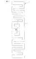
図1は、本実施の形態のRFIDインレットを示す全体平面図、図2は、図1の一部(チップ実装領域およびその近傍の整合回路部)を拡大して示す平面図である。 FIG. 1 is an overall plan view showing an RFID inlet according to the present embodiment, and FIG. 2 is an enlarged plan view showing a part of FIG. 1 (a chip mounting region and a matching circuit portion in the vicinity thereof).
本実施の形態のRFIDインレット1は、860MHz〜960MHz帯のUHF(極超短波)を使ってデータを非接触で読み書きするRFIDに適用されるものであり、厚さが50μm程度のAl(アルミニウム)箔からなるアンテナ2と、このアンテナ2の中心部に実装された半導体チップ3とによって構成されている。アンテナ2の外形は長方形であり、寸法は、長手方向が90mm、幅方向が20mmである。本実施の形態のRFIDインレット1の外観上の特徴は、広い帯域のUHF(952MHz〜954MHz)を効率よく受信できるようにするために、アンテナ2の長手方向の両側の形状を蛇行状にしたことにある。
The RFID inlet 1 of the present embodiment is applied to an RFID that reads and writes data in a non-contact manner using UHF (ultra high frequency) of 860 MHz to 960 MHz, and has an Al (aluminum) foil having a thickness of about 50 μm. And the
また、本実施の形態のRFIDインレット1は、アンテナ2と、このアンテナ2に実装された半導体チップ3のみによって構成されており、アンテナ2を支持する樹脂フィルムなどの媒体を使用していないので、部品点数が極めて少ない。しかも、アンテナ2の材料として、Cu(銅)やAu(金)のような金属箔よりも原価が安いAl箔を使用しているので、材料原価が極めて低廉であるという特徴がある。
Further, the RFID inlet 1 of the present embodiment is configured only by the
一般に、RFIDは、RFタグとリーダライタとで構成され、RFタグは、RFIDインレットとこれを物品に取り付ける媒体(ラベル、カードなど)とで構成される。UHF帯の電波を使用するRFIDは、2.45GHz帯のマイクロ波を使用するRFIDや、13.56MHz帯の短波を使用する電磁誘導方式のRFIDなどに比べて長距離の通信が可能であり、しかも多くのRFタグを同時に読み取ることができるという利点があるので、特に物流管理などの用途に好適なRFIDである。 In general, an RFID includes an RF tag and a reader / writer, and the RF tag includes an RFID inlet and a medium (label, card, etc.) for attaching the RFID tag to an article. RFID using UHF band radio waves can communicate over long distances compared to RFID using microwaves in the 2.45 GHz band and electromagnetic induction RFIDs using short waves in the 13.56 MHz band. In addition, since it has an advantage that a large number of RF tags can be read simultaneously, the RFID is particularly suitable for applications such as physical distribution management.
UHF帯の電波を使用するRFIDは、国別に利用可能な周波数帯域が割り当てられており、例えば日本には950MHz、欧州には860MHz、米国には915MHzの周波数がそれぞれ割り当てられている。そのため、例えばA国でRFIDタグを取り付けた物品をB国に輸出した場合、A国で使用している電波の周波数とB国で使用している電波の周波数の差が大きいと、B国では通信距離が大幅に短くなったり、データの読み取りが困難になったりする。 RFIDs that use UHF radio waves are assigned frequency bands that can be used by country. For example, 950 MHz is assigned to Japan, 860 MHz is assigned to Europe, and 915 MHz is assigned to the United States. For this reason, for example, when an article with an RFID tag attached in country A is exported to country B, if there is a large difference between the frequency of the radio wave used in country A and the frequency of the radio wave used in country B, The communication distance is significantly shortened, and data reading becomes difficult.
しかし、本実施の形態のRFIDインレット1は、アンテナ2の一部に図1に示すような蛇行パターンを形成しているので、RFIDが利用できる周波数帯域(860MHz〜960MHz)の全域において良好な通信特性を得ることが可能である。これにより、例えばある物品にそのデータを書き込んだRFIDインレット1を取り付けて日本から欧州に輸出した場合でも、欧州に割り当てられた周波数(860MHz)での使用を前提に作製されたリーダライタを使用してこの物品に関するデータを読み取ることが可能となる。また、例えば米国でRFIDインレット1を取り付けた物品が日本に輸入された場合でも、日本に割り当てられた周波数(950MHz)での使用を前提に作製されたリーダライタを使用してこの物品に関するデータを読み取ることが可能となる。このように、本実施の形態のRFIDインレット1は、特定の国の国内で流通する物品だけでなく、各国の間で輸出入される物品にも広く適用することができる。
However, since the RFID inlet 1 of the present embodiment has a meandering pattern as shown in FIG. 1 formed in a part of the
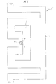
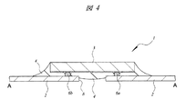
図3は、アンテナ2の中央部に実装された半導体チップ3を拡大して示す平面図、図4は、図3のA−A線に沿った断面図である。
3 is an enlarged plan view showing the
半導体チップ3は単結晶シリコンからなり、その平面寸法は、一辺が1.1mm程度の正方形である。図示は省略するが、半導体チップ3の主面には集積回路が形成されている。この集積回路は、EEPROM(Electrically Erasable Programmable ROM)などのメモリ回路、このメモリ回路を制御する制御回路、および送受信回路などからなる。メモリ回路には、RFIDインレット1が取り付けられる物品に関する各種データが書き込まれるようになっている。また、メモリ回路に書き込まれたデータを必要に応じて消去し、新たなデータを再書き込みすることもできる。
The
アンテナ2に実装された半導体チップ3の主面は、ポッティング樹脂4によって封止されている。ポッティング樹脂4は、半導体チップ3の主面に形成された集積回路や、半導体チップ3とアンテナ2との接続部などを保護するための絶縁層である。また、半導体チップ3の主面には、上記集積回路に電気的に接続された2個のAuバンプ6a、6bが形成されている。これらのAuバンプ6a、6bは、半導体チップ3の一辺の近傍に配置され、かつこの一辺に沿って並んで配置されている。Auバンプ6a、6bは、半導体チップ3の外部端子であり、その一方(Auバンプ6a)は電源端子を構成し、他方(Auバンプ6b)はGND端子を構成している。Auバンプ6a、6bは、例えば周知の電解メッキ法を用いて形成されたもので、その高さは、例えば15μm程度である。
The main surface of the
上記Auバンプ6a、6bが配置された一辺に対向する辺の近傍には、半導体チップ3内の集積回路とは電気的に接続されていないダミーのAuバンプ7a、7bが配置されている。ダミーのAuバンプ7aとダミーのAuバンプ7bとは、上記対向する辺に沿って並んで配置されている。ダミーのAuバンプ7a、7bの径および高さは、前記Auバンプ6a、6bの径および高さと同じである。
Dummy Au bumps 7a and 7b that are not electrically connected to the integrated circuit in the
後述するように、アンテナ2とAuバンプ6a、6bは、超音波圧着法によって電気的に接続されるが、その際、ダミーのAuバンプ7a、7bも同時にアンテナ2に接続される。Auバンプ6a、6bは、半導体チップ3の一辺に沿って並んで配置されているので、アンテナ2とAuバンプ6a、6bとを電気的に接続する際、半導体チップ3がアンテナ2に対して傾いた状態で接続され易く、これがアンテナ2とAuバンプ6a、6bとの接続信頼性を低下させる原因となる。そこで、Auバンプ6a、6bが配置された一辺に対向する辺の近傍にダミーのAuバンプ7a、7bを設け、Auバンプ6a、6bとダミーのAuバンプ7a、7bとを同時にアンテナ2に接続する。これにより、半導体チップ3の傾きが防止されるので、アンテナ2とAuバンプ6a、6bとの接続信頼性が向上する。このように、ダミーのAuバンプ7a、7bは、アンテナ2とAuバンプ6a、6bとを確実に接続させるために設けられる。
As will be described later, the
半導体チップ3は、その主面を下に向けた状態でアンテナ2に接続されるので、図3に示すAuバンプ6a、6bやダミーのAuバンプ7a、7bは、半導体チップ3の裏面側に配置されている。図3に示すように、半導体チップ3の電源端子を構成するAuバンプ6aとGND端子を構成するAuバンプ6bとの間の領域のアンテナ2には、Auバンプ6aとAuバンプ6bとを分離するための細いスリット8が形成されている。後述するように、スリット8は、アンテナ2を構成するAl箔の一部をプレス金型で打ち抜くことによって形成される。
Since the
また、半導体チップ3の近傍のアンテナ2には、「コ」字状のスリット9が形成されている。このスリット9が形成された領域は、主としてアンテナ2のインピーダンスを整合するための整合回路部として機能している。また、アンテナ2の長手方向の両側、すなわち蛇行パターンが形成された領域は、主としてUHFを受信する受信部として機能している。後述するように、スリット9および蛇行パターンは、アンテナ2を構成するAl箔の一部をプレス金型で打ち抜くことによって形成される。
In addition, a “U” -shaped
上記のように構成されたRFIDインレット1のデータを読み出すには、まず、リーダライタのアンテナからRFIDインレット1に950MHzの電波を送信する。すると、この電波がRFIDインレット1のアンテナ2によって受信された後、高周波電流に変換され、整合回路を通してICチップに入力される。ICチップはこの交流信号を整流して直流電力を生成し、この電力によって半導体チップ3の集積回路が動作し、メモリ回路に書き込まれたデータが半導体チップ3からアンテナ2に出力される。次に、このデータがアンテナ2から電波に乗ってリーダライタに送信されると、リーダライタは、そのアンテナを通じてこの電波を受信し、メモリ回路に書き込まれたデータを読み取る。
In order to read data of the RFID inlet 1 configured as described above, first, a radio wave of 950 MHz is transmitted from the reader / writer antenna to the RFID inlet 1. Then, after this radio wave is received by the
なお、アンテナ2のインピーダンスは、整合回路部に設けられたスリット9の形状、あるいは受信部を構成する蛇行パターンの長さや幅などが変わることによって変動する。従って、スリット9および蛇行パターンの最適な形状や寸法は、図1〜図4に示した形状や寸法に限定されるものではなく、適宜、設計変更される。
The impedance of the
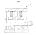
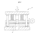
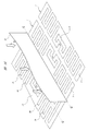
次に、上記RFIDインレット1の製造方法を説明する。RFIDインレット1を製造するには、まず、図5に示すように、ロール状に巻かれた長尺のAl箔12を用意し、このAl箔12の一端をプレス金型13のダイ14上に位置決めする。ダイ14の上方には、Al箔12を打ち抜くためのパンチ15が上下動可能に設置されている。Al箔12はアンテナ2の材料となるものであり、その厚さは、アンテナ2の厚さ(20μm程度)と同じである。また、Al箔12は、その幅がアンテナ2の長手方向の寸法(90mm)と同じになるように裁断されている。
Next, a method for manufacturing the RFID inlet 1 will be described. In order to manufacture the RFID inlet 1, first, as shown in FIG. 5, a
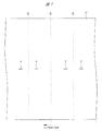
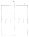
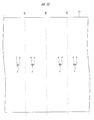
次に、図6に示すように、プレス金型13のダイ14上に位置決めされたAl箔12をパンチ15で打ち抜く。そして、Al箔12をダイ14上に送り出しながら、パンチ15による打ち抜きを繰り返すことにより、図7に示すように、Al箔12に所定の間隔で多数のスリット8を形成する。なお、図7中の破線Cは、最終工程において、Al箔12を切断金型で切断する部位を示す切断線を示している。隣り合った2つの切断線Cの間隔は、1個のアンテナ2の幅方向の寸法(20mm)と同じである。すなわち、隣り合った2つの切断線Cで区画された領域は、1個のアンテナ2が形成される領域を示している。これらの切断線Cは、Al箔12が複数のアンテナ形成領域に区画されていることを示す仮想的な線であるが、Al箔12の表面に、光学的な手段などによって検出可能な切断線Cを形成することも可能である。
Next, as shown in FIG. 6, the
特に限定はされないが、上記スリット8の形状は、長方形である。前記図3および図4に示したように、スリット8の幅は、外形寸法が1.1mm角程度の半導体チップ3よりも狭い。従って、このような微細な幅を有するスリット8の形成に用いるダイ14およびパンチ15は、後の打ち抜き工程で使用するダイおよびパンチに比べて打ち抜き精度の高いものが使用される。
Although not particularly limited, the shape of the
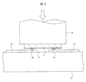
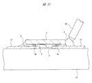
次に、図8に示すように、上記スリット8が形成された領域のAl箔12上に半導体チップ3を実装する。Al箔12上に半導体チップ3を実装するには、図9に示すように、ボンディングステージ17上にAl箔12を位置決めし、続いて、Al箔12上に半導体チップ3を位置決めする。このとき、半導体チップ3は、その主面に形成された2個のAuバンプ6a、6b(および図9には示さない2個のダミーのAuバンプ7a、7b)がスリット8を跨ぐように位置決めされる。次に、所定の温度に加熱された超音波接合ツール18を半導体チップ3の上面に圧着し、熱と超音波振動とを利用してAuバンプ6a、6b(およびダミーのAuバンプ7a、7b)とAl箔12とをAu−Al接合によって電気的に接続する。
Next, as shown in FIG. 8, the
次に、図10に示すように、Al箔12上に実装された半導体チップ3の主面をポッティング樹脂4で封止する。半導体チップ3の主面をポッティング樹脂4で封止するには、図11に示すように、半導体チップ3の実装が完了したAl箔12をステージ19上に位置決めし、続いて、樹脂塗布用ノズル20などを用いて半導体チップ3の周囲にポッティング樹脂4を供給した後、加熱または紫外線照射などによってポッティング樹脂4を硬化させる。
Next, as shown in FIG. 10, the main surface of the
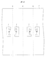
次に、図12に示すように、半導体チップ3の近傍のAl箔12に「コ」字状のスリット9を形成する。Al箔12にスリット9を形成するには、例えば前記図5および図6に示したプレス金型13にパンチおよびダイを取り付け、ダイ上に位置決めしたAl箔12をパンチで打ち抜く。このスリット9は、アンテナ2のインピーダンスを整合するために形成される。従って、スリット9の形状は「コ」字形に限定されるものではなく、適宜設計変更される。また、スリット9を形成しなくともアンテナ2のインピーダンスを最適化できる場合は、スリット9の形成工程を省くことができる。
Next, as shown in FIG. 12, a “U” -shaped
次に、図13に示すように、Al箔12に長方形のスリット10を多数形成する。これらのスリット10は、アンテナ2の長手方向の両側の形状を蛇行状にするために形成される。これらのスリット10は、切断線Cと直交する方向に延在し、切断線Cを跨ぐように配置される。また、これらのスリット10は、その長手方向の中心が切断線Cと重なるように配置される。切断線Cのそれぞれにはこのようなスリット10がその延在方向に沿って所定間隔で複数個配置される。
Next, as shown in FIG. 13, many
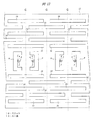
次に、図14に示すように、切断金型21を用い、Al箔12を切断線Cに沿って切断することにより、アンテナ2を個片化する。このとき、切断線Cを跨ぐように形成されていたスリット10のそれぞれは、切断線Cの両側のアンテナ2に2分割される。従って、切断線Cの両側のアンテナ2には、同時に蛇行パターンが形成される。なお、ここでは、切断金型21を用いてAl箔12を切断したが、切断線Cに沿ってAl箔12を精度よく切断できる手段であれば、いかなる手段を用いてもよい。ここまでの工程により、蛇行パターンを有するアンテナ2と、このアンテナ2に実装された半導体チップ3とからなる本実施の形態のRFIDインレット1が完成する。
Next, as shown in FIG. 14, the
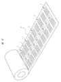
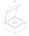
図15に示すように、完成したRFIDインレット1は、出荷に先立って粘着テープ22に貼り付けられる。多数のRFIDインレット1が貼り付けられた粘着テープ22はロール状に巻き取られた後、図16に示すように、出荷箱23などに収容されて出荷される。
As shown in FIG. 15, the completed RFID inlet 1 is affixed to the
このように、本実施の形態では、複数のスリット10をAl箔12の切断線Cに沿って所定間隔で配置すると共に、これらのスリット10を切断線Cを跨ぐように配置する。これにより、Al箔12を切断線Cに沿って切断したときに、この切断線Cの両側に形成されるアンテナ2には、蛇行状のパターンが同時に形成される。また、これら複数のスリット10は、すべて同一の形状であるため、プレス金型でスリット10を打ち抜き形成する際の金型(パンチおよびダイ)は一種類で済む。これらにより、プレス金型でスリット10を打ち抜き形成する工程が簡略化されるので、アンテナ2に蛇行パターンを形成するRFIDインレット1の製造コストを低減することができる。
Thus, in the present embodiment, the plurality of
以上、本発明者によってなされた発明を実施の形態に基づき具体的に説明したが、本発明は前記実施の形態に限定されるものではなく、その要旨を逸脱しない範囲で種々変更可能であることはいうまでもない。 As mentioned above, the invention made by the present inventor has been specifically described based on the embodiment. However, the present invention is not limited to the embodiment, and various modifications can be made without departing from the scope of the invention. Needless to say.
プレス金型を使ってAl箔12に3種類のスリット8、9、10を形成する際の順序は任意でよい。ただし、半導体チップ3の搭載領域に形成するスリット8は、極めて微細であることから、高い加工精度が要求される。一方、Al箔12に形成されるスリットの数が増えてAl箔12の面積が小さくなると、Al箔12の搬送が困難となり、プレス金型のダイとAl箔12との合わせ精度が低下する。従って、高い加工精度が要求される微細なスリット8を最初に形成した後、他のスリット9、10を形成することが望ましい。
The order in which the three types of
前記実施の形態では、UHFを使ってデータを読み書きするRFIDインレットの製造方法に適用した場合について説明したが、例えば2.45GHz帯のマイクロ波を使用するRFIDインレットや、13.56MHz帯の短波を使用する電磁誘導方式のRFIDインレットなどの製造方法に適用することもできる。 In the above embodiment, the case where the present invention is applied to a method for manufacturing an RFID inlet that reads and writes data using UHF has been described. For example, an RFID inlet that uses a 2.45 GHz band microwave or a 13.56 MHz band short wave is used. The present invention can also be applied to a manufacturing method such as an electromagnetic induction type RFID inlet used.
本発明は、特にUHF帯の電波を使用してデータを非接触で読み書きするRFIDインレットの製造に適用して有用なものである。 The present invention is particularly useful when applied to the manufacture of RFID inlets that read and write data without contact using radio waves in the UHF band.
1 RFIDインレット
2 アンテナ
3 半導体チップ
4 ポッティング樹脂
6a、6b Auバンプ
7a、7b ダミーのAuバンプ
8、9、10 スリット
12 Al箔
13 プレス金型
14 ダイ
15 パンチ
17 ボンディングステージ
18 超音波接合ツール
19 ステージ
20 樹脂塗布用ノズル
21 切断金型
22 粘着テープ
23 出荷箱
C 切断線
DESCRIPTION OF SYMBOLS 1
Claims (9)
(b)前記導体箔のそれぞれの前記アンテナ形成領域に半導体チップを実装する工程と、
(c)前記導体箔をプレス金型で打ち抜くことによって、それぞれが前記切断線を跨ぐ領域に配置され、かつ所定の間隔で前記切断線の延在方向に配列される複数の第1スリットを形成する工程と、
(d)前記工程(b)および工程(c)が完了した後、前記複数の切断線に沿って前記導体箔を切断することにより、それぞれが前記導体箔からなるアンテナと、前記アンテナに実装された前記半導体チップとによって構成される複数のRFIDインレットを得る工程と、
を含むRFIDインレットの製造方法であって、
前記工程(d)で前記導体箔を切断した際、前記複数の第1スリットのそれぞれが、互いに隣接する2つの前記アンテナ形成領域から得られた2個の前記アンテナに分離されることによって、2個の前記アンテナのそれぞれを構成する前記導体箔に蛇行パターンが同時に形成されることを特徴とするRFIDインレットの製造方法。 (A) preparing a conductor foil provided with a plurality of antenna forming regions partitioned by a plurality of cutting lines arranged in one direction at a predetermined interval;
(B) mounting a semiconductor chip on each of the antenna formation regions of the conductor foil;
(C) By punching the conductor foil with a press die, a plurality of first slits are formed which are each arranged in a region straddling the cutting line and arranged in the extending direction of the cutting line at a predetermined interval. And a process of
(D) After the step (b) and the step (c) are completed, the conductor foil is cut along the plurality of cutting lines, so that each of the antenna is made of the conductor foil, and the antenna is mounted on the antenna. Obtaining a plurality of RFID inlets constituted by the semiconductor chip;
A method of manufacturing an RFID inlet including:
When the conductor foil is cut in the step (d), each of the plurality of first slits is separated into two antennas obtained from the two antenna forming regions adjacent to each other. A method of manufacturing an RFID inlet, wherein a meandering pattern is simultaneously formed on the conductor foil constituting each of the antennas.
前記工程(b)で前記導体箔の前記アンテナ形成領域に前記半導体チップを実装する際、前記半導体チップに形成された回路の電源端子を構成する第1のバンプ電極と、前記回路のGND端子を構成する第2のバンプ電極とを前記第3のスリットを挟んで対向する領域の前記導体箔に接続することを特徴とする請求項1記載のRFIDインレットの製造方法。 Prior to the step (b), a third slit is formed in the antenna formation region of the conductor foil by punching the conductor foil with a press die,
When the semiconductor chip is mounted on the antenna formation region of the conductor foil in the step (b), a first bump electrode that constitutes a power supply terminal of a circuit formed on the semiconductor chip, and a GND terminal of the circuit 2. The method of manufacturing an RFID inlet according to claim 1, wherein the second bump electrode is connected to the conductive foil in a region facing the third bump electrode with the third slit interposed therebetween.
(a)所定の間隔で一方向に配列された複数の切断線によって区画される複数のアンテナ形成領域を備えた導体箔を用意する工程と、
(b)前記導体箔のそれぞれの前記アンテナ形成領域に半導体チップを実装する工程と、
(c)前記導体箔のそれぞれの前記アンテナ形成領域に実装された前記半導体チップを樹脂封止する工程と、
(d)前記導体箔をプレス金型で打ち抜くことによって、それぞれが前記切断線を跨ぐ領域に配置され、かつ所定の間隔で前記切断線の延在方向に配列される複数の第1スリットを形成する工程と、
(e)前記工程(b)、前記工程(c)および前記工程(d)が完了した後、前記複数の切断線に沿って前記導体箔を切断し、前記複数の第1スリットのそれぞれを前記複数の切断線のそれぞれの両側の前記アンテナ形成領域に分離することによって、前記導体箔の切断によって得られた複数のアンテナのそれぞれに同時に蛇行パターンを形成する工程と、
を含むことを特徴とするRFIDインレットの製造方法。 An RFID inlet manufacturing method comprising an antenna made of a conductive foil and a semiconductor chip mounted on the antenna,
(A) preparing a conductor foil provided with a plurality of antenna forming regions partitioned by a plurality of cutting lines arranged in one direction at a predetermined interval;
(B) mounting a semiconductor chip on each of the antenna formation regions of the conductor foil;
(C) resin-sealing the semiconductor chip mounted on the antenna formation region of each of the conductor foils;
(D) By punching out the conductive foil with a press die, a plurality of first slits are formed which are each arranged in a region straddling the cutting line and arranged in the extending direction of the cutting line at a predetermined interval. And a process of
(E) After the step (b), the step (c) and the step (d) are completed, the conductor foil is cut along the plurality of cutting lines, and the plurality of first slits are respectively Forming a meander pattern simultaneously on each of the plurality of antennas obtained by cutting the conductor foil by separating the antenna forming regions on both sides of each of the plurality of cutting lines;
A method for manufacturing an RFID inlet, comprising:
Priority Applications (1)
| Application Number | Priority Date | Filing Date | Title |
|---|---|---|---|
| JP2006180703A JP2008009801A (en) | 2006-06-30 | 2006-06-30 | Method for producing rfid inlet |
Applications Claiming Priority (1)
| Application Number | Priority Date | Filing Date | Title |
|---|---|---|---|
| JP2006180703A JP2008009801A (en) | 2006-06-30 | 2006-06-30 | Method for producing rfid inlet |
Publications (1)
| Publication Number | Publication Date |
|---|---|
| JP2008009801A true JP2008009801A (en) | 2008-01-17 |
Family
ID=39067937
Family Applications (1)
| Application Number | Title | Priority Date | Filing Date |
|---|---|---|---|
| JP2006180703A Pending JP2008009801A (en) | 2006-06-30 | 2006-06-30 | Method for producing rfid inlet |
Country Status (1)
| Country | Link |
|---|---|
| JP (1) | JP2008009801A (en) |
Cited By (6)
| Publication number | Priority date | Publication date | Assignee | Title |
|---|---|---|---|---|
| JP2009194670A (en) * | 2008-02-15 | 2009-08-27 | Fujitsu Ltd | RFID tag |
| JP2009260757A (en) * | 2008-04-18 | 2009-11-05 | Renesas Technology Corp | Inlet for rfid |
| JP4518211B2 (en) * | 2008-03-03 | 2010-08-04 | 株式会社村田製作所 | Compound antenna |
| JP2011182392A (en) * | 2010-02-08 | 2011-09-15 | Sinfonia Technology Co Ltd | Dipole-type ic tag antenna, antenna roll and method of using ic tag |
| WO2017014078A1 (en) * | 2015-07-22 | 2017-01-26 | 株式会社村田製作所 | Wireless communication device and laundry item equipped with wireless communication device |
| JP2019120972A (en) * | 2017-12-28 | 2019-07-22 | 大阪シーリング印刷株式会社 | Method for manufacturing antenna for rfid, and method for manufacturing rfid inlet |
-
2006
- 2006-06-30 JP JP2006180703A patent/JP2008009801A/en active Pending
Cited By (12)
| Publication number | Priority date | Publication date | Assignee | Title |
|---|---|---|---|---|
| JP2009194670A (en) * | 2008-02-15 | 2009-08-27 | Fujitsu Ltd | RFID tag |
| JP4518211B2 (en) * | 2008-03-03 | 2010-08-04 | 株式会社村田製作所 | Compound antenna |
| JPWO2009110382A1 (en) * | 2008-03-03 | 2011-07-14 | 株式会社村田製作所 | Compound antenna |
| JP2009260757A (en) * | 2008-04-18 | 2009-11-05 | Renesas Technology Corp | Inlet for rfid |
| JP2011182392A (en) * | 2010-02-08 | 2011-09-15 | Sinfonia Technology Co Ltd | Dipole-type ic tag antenna, antenna roll and method of using ic tag |
| US9047549B2 (en) | 2010-02-08 | 2015-06-02 | Sinfonia Technology Co., Ltd. | Antenna for dipole-type IC tag, antenna roll, and usage method for IC tag |
| WO2012108071A1 (en) * | 2011-02-08 | 2012-08-16 | シンフォニアテクノロジー株式会社 | Antenna for dipole-type ic tag, antenna roll and usage method for ic tag |
| CN103348535A (en) * | 2011-02-08 | 2013-10-09 | 昕芙旎雅有限公司 | Antenna for dipole-type ic tag, antenna roll and usage method for ic tag |
| WO2017014078A1 (en) * | 2015-07-22 | 2017-01-26 | 株式会社村田製作所 | Wireless communication device and laundry item equipped with wireless communication device |
| JPWO2017014078A1 (en) * | 2015-07-22 | 2018-03-08 | 株式会社村田製作所 | Wireless communication device and laundry article with wireless communication device |
| JP2019120972A (en) * | 2017-12-28 | 2019-07-22 | 大阪シーリング印刷株式会社 | Method for manufacturing antenna for rfid, and method for manufacturing rfid inlet |
| JP7191444B2 (en) | 2017-12-28 | 2022-12-19 | 大阪シーリング印刷株式会社 | RFID antenna manufacturing method and RFID inlet manufacturing method |
Similar Documents
| Publication | Publication Date | Title |
|---|---|---|
| US7619530B2 (en) | RFID tag | |
| US9449269B2 (en) | Methods and apparatus for embedding wire in substrates for secure documents | |
| US9171244B2 (en) | RFID tag | |
| CN101346852B (en) | Wireless IC device | |
| CN102073899B (en) | Wireless tag | |
| US20140339308A1 (en) | Rfid tag and automatic recognition system | |
| US9390365B2 (en) | Integrated circuit module for a dual-interface smart card | |
| US9373072B2 (en) | Antenna, method of manufacturing the antenna, and wireless IC device | |
| CN101228663A (en) | Radio frequency tag and method of manufacturing radio frequency tag | |
| KR20140123562A (en) | Rfid antenna module and methods | |
| JP2004062854A (en) | IC module, wireless information storage medium using the same, and wireless information transmitting / receiving device | |
| US20210365759A1 (en) | Connection bridges for dual interface transponder chip modules | |
| CN101228664A (en) | Radio frequency tag and method of manufacturing radio frequency tag | |
| WO2007034764A1 (en) | Noncontact information storage medium and method for manufacturing same | |
| JP2008009801A (en) | Method for producing rfid inlet | |
| KR100862890B1 (en) | RF antenna circuit device and RF card including same | |
| CN100412899C (en) | A method for manufacturing radio frequency identification electronic tags | |
| US11232342B2 (en) | RFID tag and method for manufacturing RFID tag | |
| JP2012094948A (en) | Inlet for non-contact communication recording medium, method of manufacturing the same, and non-contact communication recording medium | |
| JP2007233885A (en) | Inlet for rfid and manufacturing method thereof | |
| TWI803957B (en) | Rfic module and rfid transponder using the same | |
| JP4438844B2 (en) | RFID tag | |
| CN219591642U (en) | Integrated antenna | |
| JP4641095B2 (en) | Non-contact data carrier device and wiring member for booster antenna | |
| JP7115885B2 (en) | resonant circuit, antenna device |