JP2007533137A - SOI (Semiconductor Conductor Insulator) Substrate and Device Formed from This Substrate - Google Patents
SOI (Semiconductor Conductor Insulator) Substrate and Device Formed from This Substrate Download PDFInfo
- Publication number
- JP2007533137A JP2007533137A JP2007507361A JP2007507361A JP2007533137A JP 2007533137 A JP2007533137 A JP 2007533137A JP 2007507361 A JP2007507361 A JP 2007507361A JP 2007507361 A JP2007507361 A JP 2007507361A JP 2007533137 A JP2007533137 A JP 2007533137A
- Authority
- JP
- Japan
- Prior art keywords
- layer
- lattice
- silicon
- semiconductor
- semiconductor material
- Prior art date
- Legal status (The legal status is an assumption and is not a legal conclusion. Google has not performed a legal analysis and makes no representation as to the accuracy of the status listed.)
- Pending
Links
- 239000004065 semiconductor Substances 0.000 title claims abstract description 86
- 239000012212 insulator Substances 0.000 title claims abstract description 15
- 239000000758 substrate Substances 0.000 title claims description 35
- 239000004020 conductor Substances 0.000 title 1
- 239000000463 material Substances 0.000 claims abstract description 43
- 229910052761 rare earth metal Inorganic materials 0.000 claims abstract description 28
- 150000002910 rare earth metals Chemical class 0.000 claims abstract description 28
- 239000011810 insulating material Substances 0.000 claims abstract description 24
- 229910052688 Gadolinium Inorganic materials 0.000 claims abstract description 19
- UIWYJDYFSGRHKR-UHFFFAOYSA-N gadolinium atom Chemical compound [Gd] UIWYJDYFSGRHKR-UHFFFAOYSA-N 0.000 claims abstract description 19
- KBQHZAAAGSGFKK-UHFFFAOYSA-N dysprosium atom Chemical compound [Dy] KBQHZAAAGSGFKK-UHFFFAOYSA-N 0.000 claims abstract description 9
- 229910052692 Dysprosium Inorganic materials 0.000 claims abstract description 7
- 229910001279 Dy alloy Inorganic materials 0.000 claims abstract 2
- 229910000748 Gd alloy Inorganic materials 0.000 claims abstract 2
- XUIMIQQOPSSXEZ-UHFFFAOYSA-N Silicon Chemical compound [Si] XUIMIQQOPSSXEZ-UHFFFAOYSA-N 0.000 claims description 66
- 239000010703 silicon Substances 0.000 claims description 66
- 229910052710 silicon Inorganic materials 0.000 claims description 65
- 229910000577 Silicon-germanium Inorganic materials 0.000 claims description 44
- LEVVHYCKPQWKOP-UHFFFAOYSA-N [Si].[Ge] Chemical compound [Si].[Ge] LEVVHYCKPQWKOP-UHFFFAOYSA-N 0.000 claims description 43
- 238000000034 method Methods 0.000 claims description 28
- 229910045601 alloy Inorganic materials 0.000 claims description 22
- 239000000956 alloy Substances 0.000 claims description 22
- 150000001875 compounds Chemical class 0.000 claims description 6
- 229910003460 diamond Inorganic materials 0.000 abstract description 16
- 239000010432 diamond Substances 0.000 abstract description 16
- GNPVGFCGXDBREM-UHFFFAOYSA-N germanium atom Chemical group [Ge] GNPVGFCGXDBREM-UHFFFAOYSA-N 0.000 description 20
- 229910052732 germanium Inorganic materials 0.000 description 19
- 229910021332 silicide Inorganic materials 0.000 description 15
- FVBUAEGBCNSCDD-UHFFFAOYSA-N silicide(4-) Chemical compound [Si-4] FVBUAEGBCNSCDD-UHFFFAOYSA-N 0.000 description 13
- 238000004519 manufacturing process Methods 0.000 description 12
- 210000004027 cell Anatomy 0.000 description 9
- 239000013078 crystal Substances 0.000 description 9
- 230000008569 process Effects 0.000 description 8
- PXHVJJICTQNCMI-UHFFFAOYSA-N Nickel Chemical compound [Ni] PXHVJJICTQNCMI-UHFFFAOYSA-N 0.000 description 6
- 230000015572 biosynthetic process Effects 0.000 description 6
- 238000002955 isolation Methods 0.000 description 6
- 229910021420 polycrystalline silicon Inorganic materials 0.000 description 6
- 238000000151 deposition Methods 0.000 description 5
- 238000010586 diagram Methods 0.000 description 5
- 229910052751 metal Inorganic materials 0.000 description 5
- 239000002184 metal Substances 0.000 description 5
- 229920005591 polysilicon Polymers 0.000 description 5
- 125000006850 spacer group Chemical group 0.000 description 5
- 230000001681 protective effect Effects 0.000 description 4
- VYPSYNLAJGMNEJ-UHFFFAOYSA-N Silicium dioxide Chemical compound O=[Si]=O VYPSYNLAJGMNEJ-UHFFFAOYSA-N 0.000 description 3
- 238000007796 conventional method Methods 0.000 description 3
- 239000000203 mixture Substances 0.000 description 3
- 238000001451 molecular beam epitaxy Methods 0.000 description 3
- 229910021421 monocrystalline silicon Inorganic materials 0.000 description 3
- 238000004549 pulsed laser deposition Methods 0.000 description 3
- 229910052814 silicon oxide Inorganic materials 0.000 description 3
- 239000002210 silicon-based material Substances 0.000 description 3
- JBRZTFJDHDCESZ-UHFFFAOYSA-N AsGa Chemical compound [As]#[Ga] JBRZTFJDHDCESZ-UHFFFAOYSA-N 0.000 description 2
- 230000008901 benefit Effects 0.000 description 2
- 150000001768 cations Chemical class 0.000 description 2
- 238000005229 chemical vapour deposition Methods 0.000 description 2
- 229910017052 cobalt Inorganic materials 0.000 description 2
- 239000010941 cobalt Substances 0.000 description 2
- GUTLYIVDDKVIGB-UHFFFAOYSA-N cobalt atom Chemical compound [Co] GUTLYIVDDKVIGB-UHFFFAOYSA-N 0.000 description 2
- 230000008021 deposition Effects 0.000 description 2
- 230000000694 effects Effects 0.000 description 2
- 238000005530 etching Methods 0.000 description 2
- 238000002513 implantation Methods 0.000 description 2
- 238000005468 ion implantation Methods 0.000 description 2
- 238000005259 measurement Methods 0.000 description 2
- 238000002156 mixing Methods 0.000 description 2
- 229910052759 nickel Inorganic materials 0.000 description 2
- 239000002245 particle Substances 0.000 description 2
- 238000000059 patterning Methods 0.000 description 2
- 238000005498 polishing Methods 0.000 description 2
- 238000012545 processing Methods 0.000 description 2
- 229910001218 Gallium arsenide Inorganic materials 0.000 description 1
- 229910021417 amorphous silicon Inorganic materials 0.000 description 1
- 150000001450 anions Chemical class 0.000 description 1
- 230000008859 change Effects 0.000 description 1
- 238000004140 cleaning Methods 0.000 description 1
- 239000002131 composite material Substances 0.000 description 1
- 239000000470 constituent Substances 0.000 description 1
- 230000008878 coupling Effects 0.000 description 1
- 238000010168 coupling process Methods 0.000 description 1
- 238000005859 coupling reaction Methods 0.000 description 1
- 239000002019 doping agent Substances 0.000 description 1
- 230000005669 field effect Effects 0.000 description 1
- 238000011065 in-situ storage Methods 0.000 description 1
- 230000000873 masking effect Effects 0.000 description 1
- 238000012986 modification Methods 0.000 description 1
- 230000004048 modification Effects 0.000 description 1
- 230000001590 oxidative effect Effects 0.000 description 1
- 238000002161 passivation Methods 0.000 description 1
- 229920002120 photoresistant polymer Polymers 0.000 description 1
- 229920001296 polysiloxane Polymers 0.000 description 1
- 230000004044 response Effects 0.000 description 1
- 150000003376 silicon Chemical class 0.000 description 1
- 239000000126 substance Substances 0.000 description 1
- 238000006467 substitution reaction Methods 0.000 description 1
- WGPCGCOKHWGKJJ-UHFFFAOYSA-N sulfanylidenezinc Chemical compound [Zn]=S WGPCGCOKHWGKJJ-UHFFFAOYSA-N 0.000 description 1
- 229910052984 zinc sulfide Inorganic materials 0.000 description 1
Images


Classifications
-
- H—ELECTRICITY
- H01—ELECTRIC ELEMENTS
- H01L—SEMICONDUCTOR DEVICES NOT COVERED BY CLASS H10
- H01L21/00—Processes or apparatus adapted for the manufacture or treatment of semiconductor or solid state devices or of parts thereof
- H01L21/70—Manufacture or treatment of devices consisting of a plurality of solid state components formed in or on a common substrate or of parts thereof; Manufacture of integrated circuit devices or of parts thereof
- H01L21/71—Manufacture of specific parts of devices defined in group H01L21/70
- H01L21/76—Making of isolation regions between components
- H01L21/762—Dielectric regions, e.g. EPIC dielectric isolation, LOCOS; Trench refilling techniques, SOI technology, use of channel stoppers
- H01L21/7624—Dielectric regions, e.g. EPIC dielectric isolation, LOCOS; Trench refilling techniques, SOI technology, use of channel stoppers using semiconductor on insulator [SOI] technology
-
- H—ELECTRICITY
- H01—ELECTRIC ELEMENTS
- H01L—SEMICONDUCTOR DEVICES NOT COVERED BY CLASS H10
- H01L29/00—Semiconductor devices adapted for rectifying, amplifying, oscillating or switching, or capacitors or resistors with at least one potential-jump barrier or surface barrier, e.g. PN junction depletion layer or carrier concentration layer; Details of semiconductor bodies or of electrodes thereof ; Multistep manufacturing processes therefor
- H01L29/66—Types of semiconductor device ; Multistep manufacturing processes therefor
- H01L29/68—Types of semiconductor device ; Multistep manufacturing processes therefor controllable by only the electric current supplied, or only the electric potential applied, to an electrode which does not carry the current to be rectified, amplified or switched
- H01L29/76—Unipolar devices, e.g. field effect transistors
- H01L29/772—Field effect transistors
- H01L29/78—Field effect transistors with field effect produced by an insulated gate
- H01L29/7842—Field effect transistors with field effect produced by an insulated gate means for exerting mechanical stress on the crystal lattice of the channel region, e.g. using a flexible substrate
-
- H—ELECTRICITY
- H01—ELECTRIC ELEMENTS
- H01L—SEMICONDUCTOR DEVICES NOT COVERED BY CLASS H10
- H01L29/00—Semiconductor devices adapted for rectifying, amplifying, oscillating or switching, or capacitors or resistors with at least one potential-jump barrier or surface barrier, e.g. PN junction depletion layer or carrier concentration layer; Details of semiconductor bodies or of electrodes thereof ; Multistep manufacturing processes therefor
- H01L29/66—Types of semiconductor device ; Multistep manufacturing processes therefor
- H01L29/68—Types of semiconductor device ; Multistep manufacturing processes therefor controllable by only the electric current supplied, or only the electric potential applied, to an electrode which does not carry the current to be rectified, amplified or switched
- H01L29/76—Unipolar devices, e.g. field effect transistors
- H01L29/772—Field effect transistors
- H01L29/78—Field effect transistors with field effect produced by an insulated gate
- H01L29/786—Thin film transistors, i.e. transistors with a channel being at least partly a thin film
- H01L29/78603—Thin film transistors, i.e. transistors with a channel being at least partly a thin film characterised by the insulating substrate or support
-
- H—ELECTRICITY
- H01—ELECTRIC ELEMENTS
- H01L—SEMICONDUCTOR DEVICES NOT COVERED BY CLASS H10
- H01L29/00—Semiconductor devices adapted for rectifying, amplifying, oscillating or switching, or capacitors or resistors with at least one potential-jump barrier or surface barrier, e.g. PN junction depletion layer or carrier concentration layer; Details of semiconductor bodies or of electrodes thereof ; Multistep manufacturing processes therefor
- H01L29/66—Types of semiconductor device ; Multistep manufacturing processes therefor
- H01L29/68—Types of semiconductor device ; Multistep manufacturing processes therefor controllable by only the electric current supplied, or only the electric potential applied, to an electrode which does not carry the current to be rectified, amplified or switched
- H01L29/76—Unipolar devices, e.g. field effect transistors
- H01L29/772—Field effect transistors
- H01L29/78—Field effect transistors with field effect produced by an insulated gate
- H01L29/786—Thin film transistors, i.e. transistors with a channel being at least partly a thin film
- H01L29/78684—Thin film transistors, i.e. transistors with a channel being at least partly a thin film having a semiconductor body comprising semiconductor materials of Group IV not being silicon, or alloys including an element of the group IV, e.g. Ge, SiN alloys, SiC alloys
Abstract
レアアース・スカンデートのようなペロブスカイト格子構造を有する絶縁材料の層を含むSOI(semiconductor on insulator)デバイスである。この絶縁材料(52)は、この絶縁材料(52)のすぐ上にダイヤモンド格子を有する半導体材料(54)を成長させることができる、有効な格子定数を有するように選択される。レアアース・スカンデート絶縁体の例としては、ガドリニウム・スカンデート(GdScO3)、ジスプロシウム・スカンデート(DyScO3)、およびガドリニウムとジスプロシウム・スカンデートの合金(Gd1-xDyXScO3)が含まれる。An SOI (semiconductor on insulator) device including a layer of an insulating material having a perovskite lattice structure such as a rare earth scandate. The insulating material (52) is selected to have an effective lattice constant that allows a semiconductor material (54) having a diamond lattice to grow directly on the insulating material (52). Examples of rare earth scandate insulators include gadolinium scandate (GdScO 3 ), dysprosium scandate (DyScO 3 ), and alloys of gadolinium and dysprosium scandate (Gd 1-x Dy X ScO 3 ) It is.
Description
本発明は概して、絶縁ゲート型電界効果トランジスタ(MOSFET)の製造、より詳しくは、絶縁基板上に形成されるMOSFETに関する。 The present invention relates generally to the manufacture of insulated gate field effect transistors (MOSFETs), and more particularly to MOSFETs formed on an insulating substrate.
MOSFETは、集積回路(IC)の一般的な構成素子である。
図1は、従来のMOSFETデバイスを示している。
このMOSFETは、バルクシリコン基板10上の活性領域内に形成されており、この活性領域は、基板10上に製造される他のIC素子からMOSFETの活性領域を電気的に絶縁するシャロートレンチ分離領域12に囲まれている。
MOSFETは、シリコン酸化物またはシリコン酸化窒化物のような薄いゲート絶縁体18によって分離される、ゲート14およびチャネル領域16を含んでいる。ゲート14は一般的に、ポリシリコンのような高濃度にドープした半導体材料から形成される。
MOSFETのソースおよびドレイン領域は、チャネル領域16の両側に形成される浅いソースおよびドレイン領域24と、深いソース領域およびドレイン領域18とを含んでいる。
基板上の保護材料26の形成後、浅いソースおよびドレイン領域24が注入される。それからゲート14の周りにスペーサ22を形成した後、深いソースおよびドレイン領域20がイオン注入によって形成される。
ソース・シリサイドおよびドレイン・シリサイド28は、オーミックコンタクトを提供するとともに接触抵抗を減少させるべく、深いソース領域およびドレイン領域20上に形成される。
シリサイド28は、基板半導体材料およびコバルト(Co)またはニッケル(Ni)のような金属を含んでいる。シリサイド30も、ゲート14の上面に形成される。
A MOSFET is a common component of an integrated circuit (IC).
FIG. 1 shows a conventional MOSFET device.
The MOSFET is formed in an active region on the
The MOSFET includes a
The source and drain regions of the MOSFET include shallow source and
After formation of the
Source silicide and
バルク半導体基板上のデバイスの形成に変わるものとして、SOI(semiconductor on insulator)構造がある。
SOI構造において、MOSFETは、MOSFET活性領域の下にある絶縁層を含んだ基板上に形成される。
SOIデバイスは、バルク半導体基板中に形成されるデバイスに比較して多くの利点を有する。例えば、デバイス間のより良い絶縁性、リーク電流の減少、CMOS素子間のラッチアップの減少、チップキャパシタンスの減少、およびソース・ドレイン領域間の短チャネル結合の減少または除去である。
図2は、完全空乏型の一般的なSOI・MOSFETの一例を示す図である。
SOI・MOSFETは、シリコン層32および絶縁層34により構成されるSOI基板上に形成される。
MOSFET構造は、シリコン層の分離領域36上に形成される。このシリコン層は、個々のデバイスが形成される個々のアイランドを定義するようにエッチングされている。
薄い非ドープ・チャネル領域16は、シリコン領域36の中心に位置する。
ソースおよびドレイン拡張部24は、ゲート絶縁体18上に形成されたゲート14の両側におけるシリコン領域36中に注入される。
次にスペーサ22を形成し、高いソースおよびドレイン領域38をシリコン領域38上に成長させ、それから、シリサイド・ソースおよびドレインコンタクト28と、シリサイド・ゲートコンタクト30を形成する。
As an alternative to forming a device on a bulk semiconductor substrate, there is an SOI (semiconductor on insulator) structure.
In an SOI structure, the MOSFET is formed on a substrate that includes an insulating layer under the MOSFET active region.
SOI devices have many advantages over devices formed in bulk semiconductor substrates. For example, better isolation between devices, reduced leakage current, reduced latch-up between CMOS elements, reduced chip capacitance, and reduced or eliminated short channel coupling between source and drain regions.
FIG. 2 is a diagram showing an example of a general fully-depleted SOI • MOSFET.
The SOI MOSFET is formed on an SOI substrate constituted by the
The MOSFET structure is formed on the
The thin
Source and
Next,
MOSFETの性能を向上させるための1つの選択肢として、抵抗と電力消費を減少させ、駆動電流、周波数応答および動作速度を向上させるために、MOSFET半導体材料のキャリア移動度を上げることがある。最近注目を集めているキャリア移動度を増加させる方法として、引張歪みが加えられたシリコン材料を使用する方法がある。
引っ張り歪みシリコンは、シリコンゲルマニウム基板上に半導体のエピタキシャル層を成長させることによって形成することができる。
シリコンゲルマニウム格子は、格子内に大きなゲルマニウム原子が存在するため、純粋シリコン格子よりもわずかに大きい格子定数を有している。
エピタキシャル成長させたシリコンが、シリコンゲルマニウム格子に合わせて並ぶため、シリコン格子に引張歪みが生じる。
適度な引張歪みは電子移動度を増加させ、より大きな引張歪みは正孔移動度を増加させる。引張歪みの量は、シリコンゲルマニウム格子中のゲルマニウムの割合につれて増加する。また、適度な圧縮歪みが正孔移動度を改善することも知られている。
One option for improving the performance of the MOSFET is to increase the carrier mobility of the MOSFET semiconductor material in order to reduce resistance and power consumption and improve drive current, frequency response and operating speed. As a method for increasing carrier mobility, which has recently attracted attention, there is a method using a silicon material to which a tensile strain is applied.
Tensile strained silicon can be formed by growing a semiconductor epitaxial layer on a silicon germanium substrate.
The silicon germanium lattice has a slightly larger lattice constant than the pure silicon lattice because of the large germanium atoms present in the lattice.
Since the epitaxially grown silicon is aligned with the silicon germanium lattice, tensile strain occurs in the silicon lattice.
Moderate tensile strain increases electron mobility, and larger tensile strain increases hole mobility. The amount of tensile strain increases with the proportion of germanium in the silicon germanium lattice. It is also known that moderate compressive strain improves hole mobility.
引張歪みシリコン層を有するMOSFETの一例を、図3に示す。
このMOSFETは、シリコン層10上に成長するシリコンゲルマニウム層32を含んだ基板上に形成される。
シリコンゲルマニウム層は一般的に、所望する歪み量によりゲルマニウム量が0から10%〜40%に徐々に増加する、傾斜層(graded layer)である。
シリコンゲルマニウム層32上に歪みシリコン34のエピタキシャル層を成長させる。
MOSFETは、深いソースおよびドレイン領域20、浅いソースおよびドレイン拡張部24、ゲート酸化層18、保護材料26に囲まれたゲート14、スペーサ22、ソースおよびドレインシリサイド28、ゲートシリサイド30、およびシャロートレンチ分離12を含む従来のMOSFET構造を使用する。
チャネル領域16中の歪みシリコン材料は、ソースおよびドレインの間のキャリア移動度を高める。
An example of a MOSFET having a tensile strained silicon layer is shown in FIG.
The MOSFET is formed on a substrate including a
The silicon germanium layer is generally a graded layer where the germanium content gradually increases from 0 to 10% to 40% depending on the amount of strain desired.
An epitaxial layer of
The MOSFET includes a deep source and
The strained silicon material in the
歪みシリコンはまた、SOI基板上に形成されるMOSFETに組み入れられてもよい。
図4は、歪みシリコンSOIMOSFETの一例を示す図である。
このデバイスでは、MOSFETは、絶縁層40に重なるシリコンゲルマニウム層を含むSOI基板上に形成される。
シリコンゲルマニウム層をパターン化し、その上に個々のMOSFETが形成される分離領域42を定義する。
歪みシリコン層44を、シリコンゲルマニウム領域42上に成長させる。
その後、図3の従来の歪みシリコンデバイスの形成方法に類する方法で、MOSFETを形成する。
Strained silicon may also be incorporated into MOSFETs formed on SOI substrates.
FIG. 4 is a diagram illustrating an example of a strained silicon SOIMOSFET.
In this device, the MOSFET is formed on an SOI substrate that includes a silicon germanium layer overlying the
The silicon germanium layer is patterned to define
A
Thereafter, a MOSFET is formed by a method similar to the conventional method for forming a strained silicon device of FIG.
歪みシリコンチャネルを組み入れた完全空乏型のSOIデバイスを形成するのは難しい。
短チャネル効果を制御するために、完全空乏型のSOI・MOSFETの厚さは、チャネル領域がチャネル長の約3分の1を超えない厚さとすることが好ましい。
しかしながら、歪みシリコンチャネルの下のシリコンゲルマニウムに支持層を提供する必要があるため、全体のチャネル厚さはチャネル長に対する制限となる。または、歪みシリコンの厚さは移動度をかなり高めるためには十分ではない。
It is difficult to form fully depleted SOI devices that incorporate strained silicon channels.
In order to control the short channel effect, the thickness of the fully depleted SOI • MOSFET is preferably set such that the channel region does not exceed about one third of the channel length.
However, the overall channel thickness is a limitation on the channel length because it is necessary to provide a support layer for silicon germanium under the strained silicon channel. Alternatively, the strained silicon thickness is not sufficient to significantly increase mobility.
他の条件は一般的に、SOIデバイスの小型化に対するさらなる障害となる。
従来の完全空乏型のSOIデバイスでは、半導体の所望の厚さになるまで基板上の化学的機械的研磨(CMP)を実行することにより、非常に薄いチャネル層を製造することが一般的である。
しかしながら、CMPにより、その厚さに100Å程度の間のばらつきを有し得る、均一でない表面が製造される。
クリティカルディメンションが減少されるにつれて、このような厚さのばらつきは許容できないものとなる。例えば、45nmのデバイスについては、チャネル領域の厚さは約150Åであることが望ましい。
研磨した層の厚さにばらつきがあれば、これらのディメンションにおいて正確な厚さを有しているチャネル層を確実に製造するのは非常に難しい。
Other conditions are generally an additional obstacle to the miniaturization of SOI devices.
In conventional fully depleted SOI devices, it is common to produce a very thin channel layer by performing chemical mechanical polishing (CMP) on the substrate until the desired semiconductor thickness is achieved. .
However, CMP produces a non-uniform surface that can have a variation of as much as 100 mm in thickness.
As the critical dimension is reduced, such thickness variations become unacceptable. For example, for a 45 nm device, the channel region thickness is desirably about 150 mm.
Given the variation in the thickness of the polished layer, it is very difficult to reliably produce a channel layer having an accurate thickness in these dimensions.
実質的にチャネル領域の厚さを一定にするために、絶縁材料上に半導体の層を成長させることは望ましいであろう。
しかしながら、従来の半導体デバイス製造技術は、さらなる結晶質の成長におけるテンプレートとして結晶格子を使用する。
例えば、シリコンウェーハは、規則的な結晶格子を提供するように、結晶面のうちの1つに沿ってカットされる単結晶シリコンから構成される。
この格子は、たい積されるシリコンの原子に対してのテンプレートとして役立つ。または、同じ格子構造を有している他の元素は、たい積において整列するであろう。このように、さらなる単結晶材料を形成する。
このようなテンプレートがない状態でたい積されたシリコンは、多結晶シリコンまたはアモルファス・シリコンの形態をとる。これは、周囲の粒子に関してランダムに方向付けられた結晶格子をそれぞれ有する個々の粒子から形成される。
シリコンのこれらの形態は、単結晶シリコンと比較して低い導電率を呈する。したがって、これらをMOSFETの活性領域において使用することは望ましくない。
このように、現在のところ、他の材料、特に、実質的にアモルファスであるか、シリコン格子と一致しない構造を有する酸化シリコンやシリコン酸化窒化物のような従来の絶縁体上に単結晶シリコンを成長させることは、一般的に可能ではなかった。
It may be desirable to grow a layer of semiconductor on the insulating material in order to make the thickness of the channel region substantially constant.
However, conventional semiconductor device manufacturing techniques use the crystal lattice as a template in further crystalline growth.
For example, a silicon wafer is composed of single crystal silicon that is cut along one of the crystal planes to provide a regular crystal lattice.
This lattice serves as a template for the silicon atoms to be deposited. Or other elements having the same lattice structure will align in the stack. In this way, a further single crystal material is formed.
Silicon deposited in the absence of such a template takes the form of polycrystalline silicon or amorphous silicon. It is formed from individual particles each having a crystal lattice that is randomly oriented with respect to surrounding particles.
These forms of silicon exhibit a lower conductivity compared to single crystal silicon. Therefore, it is not desirable to use them in the active region of the MOSFET.
As such, single crystal silicon is currently on other materials, particularly conventional insulators such as silicon oxide and silicon oxynitride that are substantially amorphous or have a structure that does not match the silicon lattice. Growing was generally not possible.
したがって、絶縁デバイス上に半導体を製造するための従来の技術は、小さなクリティカルディメンションを有するデバイスや、歪みシリコンが組み入れられたデバイスを製造するには十分ではない。 Thus, conventional techniques for manufacturing semiconductors on isolated devices are not sufficient to manufacture devices with small critical dimensions or devices incorporating strained silicon.
本発明の実施形態は、その上に半導体層を直接成長させることができる絶縁層を含む、SOI(semiconductor on insulator)デバイスを提供する。
絶縁層が半導体材料に引張歪みまたは圧縮歪みを与えるように、絶縁層の特性および半導体層の特性を選ぶことができる。
Embodiments of the present invention provide an SOI (semiconductor on insulator) device that includes an insulating layer on which a semiconductor layer can be grown directly.
The properties of the insulating layer and the semiconductor layer can be selected such that the insulating layer imparts tensile strain or compressive strain to the semiconductor material.
本発明のさらなる実施形態は、上述のようなデバイスを形成する方法を提供する。
本発明の好ましい一実施形態は、ペロブスカイト(perovskite)格子構造を有する絶縁材料の層を利用する。このペロブスカイト格子は、ダイヤモンド格子半導体を成長させるのに適したテンプレートを提供することが分かっている。
ペロブスカイト格子構造を有している絶縁体の例には、ガドリニウム・スカンデート(GdScO3)、ジスプロシウム・スカンデート(DyScO3)のようなレアアース・スカンデート(rare earth scandate)や、ガドリニウムとジスプロシウム・スカンデートの合金(Gd1-xDyXScO3)が含まれる。
レアアース・スカンデートに互換性を有する(compartible)ダイヤモンド格子構造を有している半導体の例には、シリコン、ゲルマニウム、シリコンとゲルマニウムの合金、および砒化ガリウムのようなIII-V型半導体が含まれる。
レアアース・スカンデートと半導体材料の化学量論組成は、レアアース・スカンデートがその上に成長させた半導体材料に引張歪みまたは圧縮歪みを与えるように、設計することができる。
このような絶縁材料は、SOI・MOSFET中の絶縁層として使用することができ、薄い半導体層を絶縁層上に直接成長させることができる。
A further embodiment of the invention provides a method of forming a device as described above.
One preferred embodiment of the present invention utilizes a layer of insulating material having a perovskite lattice structure. This perovskite lattice has been found to provide a suitable template for growing diamond lattice semiconductors.
Examples of insulators having a perovskite lattice structure, gadolinium scandate (GdScO 3), rare earth-scandate (rare earth scandate), such as a dysprosium-scandate (DyScO 3) and, gadolinium and dysprosium Scandate alloys (Gd 1-x Dy X ScO 3 ) are included.
Examples of semiconductors having diamond lattice structures that are compatible with rare earth scandates include silicon, germanium, silicon-germanium alloys, and III-V type semiconductors such as gallium arsenide. .
The stoichiometric composition of the rare earth scandate and the semiconductor material can be designed such that the rare earth scandate imparts tensile or compressive strain to the semiconductor material grown thereon.
Such an insulating material can be used as an insulating layer in an SOI.MOSFET, and a thin semiconductor layer can be directly grown on the insulating layer.
本発明の実施形態によれば、ダイヤモンド格子を有する単結晶半導体材料を、ペロブスカイト格子を有する絶縁層上に成長させることができる。
ダイヤモンド格子を有する半導体は、シリコン、ゲルマニウムおよびシリコンゲルマニウム合金を含んでいる。
閃亜鉛鉱(zinc blende)格子と呼ばれることのある一種のダイヤモンド格子を有している化合物半導体はまた、ペロブスカイト格子上に成長させることができ、この出願においてはダイヤモンド格子を有すると考えられるであろう。
このような化合物半導体の一例は、あるII-VIタイプの半導体と同様に、砒化ガリウム(GaAs)のようなIII-Vタイプの半導体を含んでいる。
ペロブスカイト格子構造を有している絶縁体の例には、ガドリニウム・スカンデート(GdScO3)、ジスプロシウム・スカンデート(DyScO3)、およびガドリニウムおよびジスプロシウム・スカンデート(Gd1-xDyXScO3)の合金のような、レアアース・スカンデート合成物が含まれる。
レアアース・スカンデートと半導体材料の化学量論組成は、レアアース・スカンデートがその上に成長させた半導体材料に引張歪みまたは圧縮歪みを与えるように、設計することができる。
According to an embodiment of the present invention, a single crystal semiconductor material having a diamond lattice can be grown on an insulating layer having a perovskite lattice.
Semiconductors having a diamond lattice include silicon, germanium and silicon germanium alloys.
A compound semiconductor having a kind of diamond lattice, sometimes called a zinc blende lattice, can also be grown on a perovskite lattice, and in this application would be considered to have a diamond lattice. Let's go.
An example of such a compound semiconductor includes a III-V type semiconductor such as gallium arsenide (GaAs) as well as certain II-VI type semiconductors.
Examples of insulators having a perovskite lattice structure include gadolinium scandate (GdScO 3 ), dysprosium scandate (DyScO 3 ), and gadolinium and dysprosium scandate (Gd 1-x Dy X ScO 3 ) Rare earth scandate composites, such as
The stoichiometric composition of the rare earth scandate and the semiconductor material can be designed such that the rare earth scandate imparts tensile or compressive strain to the semiconductor material grown thereon.
ある実施形態の一例においては、レアアース・スカンデート・ガドリニウム・スカンデート(GdScO3)の層は、引張り歪みシリコンまたはシリコンゲルマニウム層の成長のための絶縁層および支持層として使用される。
単結晶ガドリニウム・スカンデートは、22から35の誘電率を有しているので、SOI用の優れた絶縁材料である。
In one example embodiment, a layer of rare earth scandate gadolinium scandate (GdScO 3 ) is used as an insulating and support layer for the growth of tensile strained silicon or silicon germanium layers.
Single crystal gadolinium scandate has a dielectric constant between 22 and 35 and is therefore an excellent insulating material for SOI.
図5aは、ガドリニウム・スカンデート(GdScO3)のペロブスカイト格子中の単位胞(単位格子)の(001)面(フェース)を示している。
その理想的な形状において、ペロブスカイト格子は、Pm3m対称性(Pm3m symmetry)を有している。換言すると、格子の単位胞は、立方体の中心にカチオンのうちの一方(例えば、Gd)があり、各端部にカチオンのうちの他方(例えば、Sc)があり、各端部に沿った中心にアニオン(O)を有する立方体である。
ほとんどのペロブスカイト格子において、格子は、格子中における特定の原子により、完全な立方体の形状から多少歪められるが、全体的な構造は同じままである。したがって単位格子の面は、面心原子がなく、実質的に正方形である。
FIG. 5a shows the (001) plane (face) of the unit cell (unit cell) in the perovskite lattice of gadolinium scandate (GdScO 3 ).
In its ideal shape, the perovskite lattice has Pm3m symmetry. In other words, the unit cell of the lattice has one of the cations (eg, Gd) at the center of the cube, the other of the cations (eg, Sc) at each end, and the center along each end Is a cube having an anion (O).
In most perovskite lattices, the lattice is somewhat distorted from the complete cubic shape by certain atoms in the lattice, but the overall structure remains the same. Therefore, the plane of the unit cell is substantially square with no face-centered atoms.
図5bは、シリコンのダイヤモンド格子中の単位胞の(001)面を示している。
ダイヤモンド格子は実質的に、2つの互いに貫入する(interpenetrating)面心立方格子で構成されており、これらの格子はそれぞれ、3つの空間軸のそれぞれの軸に沿った格子定数の長さの4分の1だけ、他の格子からずれて(オフセットされて)いる。
FIG. 5b shows the (001) plane of the unit cell in a silicon diamond lattice.
The diamond lattice is essentially composed of two interpenetrating face-centered cubic lattices, each of which is a quarter of the length of the lattice constant along each of the three spatial axes. Is offset (offset) from the other grids.
ダイヤモンド格子は、ペロブスカイト格子と構造上異なるが、この2つの格子は、各格子中の原子の間隔に基づきエピタキシャル成長させるという目的において互換性を有する。
図5cに示すように、ガドリニウム・スカンデート格子の(001)平面に対して、シリコン格子の(001)平面を、45°回転させる場合、シリコン・ダイヤモンド格子の面の原子は、ガドリニウム・スカンデート・ペロブスカイト格子の空いている面に沿って並ぶ。
このように、ガドリニウム・スカンデート格子は、シリコンを成長させるためのテンプレートとして役立つことができる。
Although the diamond lattice is structurally different from the perovskite lattice, the two lattices are compatible for the purpose of epitaxial growth based on the spacing of atoms in each lattice.
As shown in FIG. 5c, when the (001) plane of the silicon lattice is rotated by 45 ° with respect to the (001) plane of the gadolinium scandate lattice, the atoms on the surface of the silicon diamond lattice are gadolinium scandate. Line up along the vacant surface of the perovskite lattice.
Thus, the gadolinium scandate lattice can serve as a template for growing silicon.
図5aに示すように、ガドリニウム・スカンデート格子の(001)面の格子定数は、3.94Åである。また、図5bに示すように、緩和シリコン格子の(001)面の格子定数は、5.431Åである。
しかしながら、ガドリニウム・スカンデート格子中の面の中心部分の間の対角線の距離は、5.572Åである。これは、純粋な緩和シリコンの格子定数である5.431Åよりも約2.7%大きい。
比較のため、純粋な緩和ゲルマニウムは、5.657Åのゲルマニウム格子定数を有している。これはシリコンの格子定数よりも約4.2%大きい。
従来の歪みシリコンデバイスは、シリコンとゲルマニウムの2つ格子定数の値の間にあるとともに格子中のゲルマニウムの量に依存する格子定数を有する、シリコンゲルマニウムSi1-XGeXの支持層を使用する。
従来の歪みシリコンデバイスにおいては、ゲルマニウムの比率は一般的に約10%から40%の間にあり、シリコンの格子定数よりも実際上0.9%から1.7%大きい格子定数を有する格子となってしまう。
As shown in FIG. 5a, the lattice constant of the (001) plane of the gadolinium-scandate lattice is 3.94. Also, as shown in FIG. 5b, the lattice constant of the (001) plane of the relaxed silicon lattice is 5.431.
However, the diagonal distance between the central portions of the faces in the gadolinium scandate lattice is 5.57257. This is approximately 2.7% greater than the pure lattice constant of 5.431Å.
For comparison, pure relaxed germanium has a germanium lattice constant of 5.657Å. This is about 4.2% larger than the lattice constant of silicon.
Conventional strained silicon devices use a silicon germanium Si 1-X Ge X support layer that has a lattice constant that is between the two lattice constant values of silicon and germanium and depends on the amount of germanium in the lattice. .
In conventional strained silicon devices, the germanium ratio is typically between about 10% and 40%, with a lattice having a lattice constant that is actually 0.9% to 1.7% greater than that of silicon. turn into.
ペロブスカイト格子とダイヤモンド格子の間の格子不整合を特徴づけるべく、本願においては、ペロブスカイト格子の「有効な格子定数」と呼ばれる量を利用する。
実質的に立方体の単位胞を有するペロブスカイト格子では、有効な格子定数は、対角線上に方向付けられる単位胞の面の中心部分の間の距離として定義することができる。
立方体の形状からいくらか歪められ、このように異なる長さの対角線を備えるダイヤモンド形状の単位胞面を有しているペロブスカイト格子においては、面の中心部分間の対角線の距離は、測定する方向に依存するであろう。
このような場合、有効な格子定数は、面の中心部分間の2つの対角線の距離の平均として定義することができる。
しかしながら、この特性が活用される実施形態においては、他方向の長さと比較して一方向の長さの方を長くする方法で、重なる半導体格子に歪みを与えることが所望される実施例のように、有効な格子定数は、より大きな距離またはより少ない距離の方向において対角線の面の中心部分の間の距離として定義することができる。
In order to characterize the lattice mismatch between the perovskite lattice and the diamond lattice, the present application utilizes a quantity called the “effective lattice constant” of the perovskite lattice.
In a perovskite lattice having a substantially cubic unit cell, the effective lattice constant can be defined as the distance between the central portions of the face of the unit cell oriented diagonally.
In a perovskite lattice that is somewhat distorted from the cubic shape and thus has a diamond-shaped unit cell surface with diagonals of different lengths, the diagonal distance between the central parts of the surface depends on the direction of measurement. Will do.
In such a case, the effective lattice constant can be defined as the average of the two diagonal distances between the central portions of the surface.
However, in an embodiment in which this characteristic is utilized, as in an embodiment in which it is desired to strain an overlapping semiconductor lattice by a method in which the length in one direction is longer than the length in another direction. In addition, the effective lattice constant can be defined as the distance between the central portions of the diagonal faces in the direction of greater or lesser distances.
上述の測定の一例は、GdScO3に特有のものである。また、異なる有効な格子定数を備えた他のレアアース・スカンデートは、エピタキシャル半導体格子についてずれの程度を所望のものとするように形成することができる。
例えば、ジスプロシウム・スカンデート(DyScO3)を代わりに使用することができる。DyScO3は、約5.6Åの有効な格子定数を有している。
さらに他の例では、Gd1-XDyXScO3のようなレアアース・スカンデート合金を、所望の有効な格子定数を提供するように選択されたガドリニウムおよびジスプロシウムの化学量論比で設計することができる。
一般に、レアアース・スカンデート絶縁体上に引張り歪みシリコンを成長させることを含む使用状況については、レアアース・スカンデートの有効な格子定数は、緩和シリコンの格子定数(5.431Å)よりも大きいことが好ましく、緩和ゲルマニウムの格子定数(5.657Å)未満であることが好ましく、40%のゲルマニウムからなる緩和シリコンゲルマニウム合金の格子定数(5.519Å)未満であることがさらに好ましい。
An example of the above measurement is specific to GdScO 3 . Also, other rare earth scandates with different effective lattice constants can be formed to achieve the desired degree of deviation for the epitaxial semiconductor lattice.
For example, dysprosium scandate (DyScO 3 ) can be used instead. DyScO 3 has an effective lattice constant of about 5.6Å.
In yet another example, a rare earth scandate alloy such as Gd 1-X Dy X ScO 3 is designed with a stoichiometric ratio of gadolinium and dysprosium selected to provide the desired effective lattice constant. Can do.
In general, for use situations involving growing tensile strained silicon on rare earth scandate insulators, the effective lattice constant of rare earth scandates may be greater than the lattice constant of relaxed silicon (5.43143). Preferably, it is less than the lattice constant (5.5575) of relaxed germanium, and more preferably less than the lattice constant (5.519Å) of a relaxed silicon germanium alloy composed of 40% germanium.
レアアース・スカンデートのようなペロブスカイト格子構造を有する絶縁層の使用することにより、シリコン、ゲルマニウム、シリコンゲルマニウム合金、または化合物半導体材料を絶縁材料上に直接成長させることができる。
シリコンゲルマニウム合金中のシリコンおよびゲルマニウムの比率は、様々な効果を生成するように、絶縁基板の有効な格子定数に関して選択することができる。
例えば、絶縁材料の有効な格子定数よりも小さい格子定数を有するように、シリコンゲルマニウム合金を形成することができ、その結果、シリコンゲルマニウム合金中に所望の量の引張歪みを与えることになるようにしてもよい。
他の例においては、絶縁材料の有効な格子定数よりも大きな格子定数を有するように、シリコンゲルマニウム合金を形成することができ、その結果、シリコンゲルマニウム合金上に所望の量の圧縮歪みを与えることになるようにしてもよい。
圧縮歪みゲルマニウムはまた、レアアース・スカンデート絶縁体上に成長させることができる。
さらに、所与の有効な格子定数を備えたレアアース・スカンデートの層を有する基板が与えられた場合、引張りおよび圧縮歪み半導体が共存している領域を提供するように、異なる理論混合比を有するシリコンおよびシリコンゲルマニウム合金を、基板上の選択された場所で成長させることができる。
これらは例えば、高い電子移動度を提供する引張り歪みチャネルを有するNMOSデバイスおよび高い正孔移動度を提供する圧縮歪みチャネルを有するPMOSデバイスを含むCMOSデバイスを製造するのに使用することができる。
By using an insulating layer having a perovskite lattice structure such as rare earth scandate, silicon, germanium, a silicon germanium alloy, or a compound semiconductor material can be directly grown on the insulating material.
The ratio of silicon and germanium in the silicon germanium alloy can be selected with respect to the effective lattice constant of the insulating substrate so as to produce various effects.
For example, a silicon germanium alloy can be formed to have a lattice constant that is less than the effective lattice constant of the insulating material, resulting in a desired amount of tensile strain in the silicon germanium alloy. May be.
In other examples, the silicon germanium alloy can be formed to have a lattice constant greater than the effective lattice constant of the insulating material, resulting in a desired amount of compressive strain on the silicon germanium alloy. It may be made to become.
Compressive strained germanium can also be grown on rare earth scandate insulators.
In addition, given a substrate having a layer of rare earth scandate with a given effective lattice constant, it has different theoretical mixing ratios to provide regions where tensile and compressive strained semiconductors coexist. Silicon and silicon germanium alloys can be grown at selected locations on the substrate.
They can be used, for example, to fabricate CMOS devices including NMOS devices having tensile strained channels that provide high electron mobility and PMOS devices having compressive strained channels that provide high hole mobility.
ガドリニウム・スカンデート絶縁層または他のレアアース・スカンデート絶縁層を含むSOI基板は、多くの方法により製造することができる。
ガドリニウム・スカンデートは、分子線エピタキシーによってたい積することができる。本質的な構成元素のそれぞれのビーム線は、超高真空によって、化学量論の量においてそれらが化学結合する基板部分に向けられる。
また、他の例においては、ガドリニウム・スカンデート・ターゲットを紫外線レーザによって蒸発させ、基板面上に再結晶させる、パルスレーザたい積を使用してよい。
パルスレーザたい積は、より早く成長させることができるため、分子線エピタキシーよりも好ましいものとなり得る。また、化学蒸着法が使用されてもよい。
これらの方法が比較的平坦な表面を有する絶縁層を形成することに注目すべきである。
絶縁層上にその後成長させた半導体層は、研磨により薄くなった層よりも実質的に厚さのばらつきが少ない。
An SOI substrate including a gadolinium scandate insulating layer or other rare earth scandate insulating layer can be manufactured by a number of methods.
Gadolinium scandate can be deposited by molecular beam epitaxy. Each beam line of the essential constituent elements is directed by ultrahigh vacuum to the portion of the substrate to which they are chemically bonded in a stoichiometric amount.
In another example, a pulsed laser deposition may be used in which the gadolinium scandate target is evaporated by an ultraviolet laser and recrystallized on the substrate surface.
Pulsed laser deposition can be preferred over molecular beam epitaxy because it can be grown faster. Chemical vapor deposition may also be used.
It should be noted that these methods form an insulating layer having a relatively flat surface.
The semiconductor layer subsequently grown on the insulating layer has substantially less thickness variation than the layer thinned by polishing.
一般的に、レアアース・スカンデート層は、その表面にシリコンゲルマニウム層を有している基板上に形成される。
このシリコンゲルマニウム層は一般的に、ゲルマニウムの含有率が0%から所望の%まで徐々に増加する段階的な方法で、シリコンウェーハ上に成長させられる。この方法は、所望の格子定数を有する緩和シリコンゲルマニウム層を成長できるようにする。
その後、レアアース・スカンデートを、例えば上述した技術のうちの1つによって、シリコンゲルマニウム層上に形成する。
実装によっては、シリコンゲルマニウム層は、レアアース・スカンデートの有効な格子定数と一致するように形成されてもよいし、または、レアアース・スカンデート格子を圧縮するとともにその有効な格子定数を減少させるべく、シリコンゲルマニウム層は、レアアース・スカンデートの有効な格子定数よりも小さい格子定数を有するように形成されてもよい。
In general, the rare earth scandate layer is formed on a substrate having a silicon germanium layer on the surface thereof.
This silicon germanium layer is generally grown on a silicon wafer in a stepwise manner in which the germanium content gradually increases from 0% to the desired%. This method allows growth of relaxed silicon germanium layers having the desired lattice constant.
A rare earth scandate is then formed on the silicon germanium layer, for example, by one of the techniques described above.
Depending on the implementation, the silicon germanium layer may be formed to match the effective lattice constant of the rare earth scandate, or to compress the rare earth scandate lattice and reduce its effective lattice constant. The silicon germanium layer may be formed to have a lattice constant smaller than the effective lattice constant of the rare earth scandate.
図6aないし図6fは、本発明の実施例の一例による、引張り歪みSOI・MOSFETの製造中に形成される構造を示す図である。
図6aは、シリコンゲルマニウム層50含むSOI基板を示す。上述したように、シリコンゲルマニウム層50は一般的に、シリコンウェーハ上に成長させられ、所望の格子定数を提供する、表面におけるゲルマニウムの含有率を有する傾斜組成を有している。
例えば、ある実施形態の一例においては、シリコンゲルマニウム層の表面は、約20%のゲルマニウムにより構成された緩和シリコンゲルマニウム合金とすることができる。
6a to 6f are diagrams illustrating structures formed during the manufacture of a tensile strained SOI.MOSFET according to an example embodiment of the present invention.
FIG. 6 a shows an SOI substrate including a
For example, in one example embodiment, the surface of the silicon germanium layer can be a relaxed silicon germanium alloy composed of about 20% germanium.
ペロブスカイト格子を有する材料の絶縁層52は、シリコンゲルマニウム層50上に形成される。ある実施形態の一例においては、この絶縁材料は、ガドリニウム・スカンデートのようなレアアース・スカンデートである。
絶縁層52は、分子線エピタキシー、パルスレーザたい積、または化学蒸着法のような様々な技術によって形成することができる。
ある実施形態の一例においては、ガドリニウム・スカンデート層は、100Åから200Åの間の厚さに形成される。
An insulating
The insulating
In one example embodiment, the gadolinium scandate layer is formed to a thickness between 100 and 200 inches.
半導体層54は、絶縁層52上に成長させられる。この半導体層54は、単結晶層であり、シリコン、ゲルマニウム、シリコンゲルマニウム合金、III-VまたはII-VIタイプのような化合物半導体、またはダイヤモンド格子を有する別の半導体から形成することができる。
半導体層の厚さは、特定の実施形態により選択され得る。ある実施形態の一例においては、半導体層は、約200Åの厚さを有するシリコン層である。
完全空乏型のSOIデバイスでは、半導体層54は一般的にドープされていないが、ドーピングは、特定の実施形態に従って実行されてもよい。
The
The thickness of the semiconductor layer can be selected according to a particular embodiment. In one example embodiment, the semiconductor layer is a silicon layer having a thickness of about 200 mm.
In fully depleted SOI devices, the
図6bは、その上に個々のデバイスが形成されることになる半導体材料の分離アイランドを形成するように、半導体層54を選択エッチングした後の図6aの構造を示す図である。
FIG. 6b shows the structure of FIG. 6a after selective etching of the
図6cは、半導体層54上にゲート絶縁層56を形成し、ゲート絶縁層56上にポリシリコン・ゲート58をたい積した後の図6bの構造を示す図である。
ゲート絶縁層56は、半導体層54を熱酸化させるか、絶縁材料をたい積することによって成長させることができる。
ポリシリコン・ゲートは、ポリシリコン層を全体的にたい積した後、ポリシリコン層をパターニングすることによって形成してよい。
FIG. 6 c shows the structure of FIG. 6 b after forming a
The
The polysilicon gate may be formed by depositing the polysilicon layer as a whole and then patterning the polysilicon layer.
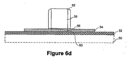
図6dは、ゲート58の両側における半導体層54中にソースおよびドレイン拡張部60を形成すべく、イオン注入によってドーパントを注入し、その後ゲート58の周りにスペーサ62を形成した後の、図6Cの構造を示す図である。
ゲート58は、ソースおよびドレイン拡張部60の注入の間、チャネル領域を被覆する。
スペーサ62は、酸化シリコンを全体的にたい積した後、水平面から酸化物を除去するように、方向性のあるエッチバックプロセスを実行することによって形成することができる。
FIG. 6d is a view of FIG. 6C after dopants have been implanted by ion implantation to form source and
The
The
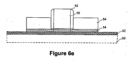
図6eは、ゲート58の両側の隣接部分に、半導体層54に接する高いソースおよびドレイン領域64を形成した後の図6dの構造を示す図である。
高いソースおよびドレイン領域64は、シリコンの選択エピタキシャル成長によって成長させることができる。
一般的に、半導体層54上のシリコンの成長率は、周囲の露出した絶縁層52上のシリコンの成長率よりもずっと大きい。さらに、成長室中の雰囲気は一般的に、HClを含んでいる。このHClにより、たい積されたシリコンのエッチングの程度が決まる。
たい積パラメータの制御を通じて、エピタキシャル成長プロセスは、絶縁層52の露出部分上に、実質的に成長量0のシリコンを製造するのに最適化することができる。
他の例では、絶縁層52上に蓄積したシリコンをすべて除去するように、高いソースおよびドレイン領域64を形成した後、短いエッチ・バックを実行してよい。
このソースおよびドレイン領域64は、その場(インサイチュー)で、または注入プロセスによってドープされ得る。
FIG. 6e shows the structure of FIG. 6d after forming high source and drain
High source and drain
In general, the growth rate of silicon on the
Through control of the deposition parameters, the epitaxial growth process can be optimized to produce substantially zero growth of silicon on the exposed portion of the insulating
In another example, a short etch back may be performed after the high source and drain
This source and drain
図6fは、ソースおよびドレイン・シリサイド66およびゲート・シリサイド68を形成した後の、図6eの構造を示す図である。
シリサイド66および68は、ゲート58、ソースおよびドレイン領域64のシリコン材料と、コバルト(Co)またはニッケル(Ni)のような金属と、を含む化合物から形成される。
シリサイド66および68は、構造全体の上に金属の薄い共形層をたい積し、金属と下にある半導体材料との間の接点においてシリサイド形成を促進するようにアニーリングし、その後、余った金属を除去することにより形成される。
ソースおよびドレイン領域とゲートのシリサイドが形成されることになっている部分から酸化物と保護材料を除去するパターニング・ステップは、一般的にシリサイドを形成する前に実行される。
FIG. 6f shows the structure of FIG. 6e after source and drain
Silicides 66 and 68 are formed from a compound that includes the silicon material of
Silicides 66 and 68 deposit a thin conformal layer of metal over the entire structure and anneal to promote silicide formation at the contact between the metal and the underlying semiconductor material, after which the excess metal is removed. It is formed by removing.
The patterning step of removing the oxide and protective material from the source and drain regions and the portion of the gate where the silicide is to be formed is generally performed prior to forming the silicide.
図6aないし図6fのプロセスは、シリコンゲルマニウムの層上に形成されるレアアース・スカンデートの層からなるSOI基板を使用しているMOSFET形成の一例を示している。しかしながら、様々な他のMOSFET構造を形成してもよい。
概略的には、本発明の実施形態による電子デバイスは、ペロブスカイト格子を有する絶縁材料の層を含んでいる基板と、ペロブスカイト材料の層上に形成される単結晶半導体材料の層とを含む。
そのチャネル領域中に半導体を組み入れるMOSFETを、基板上に形成してよい。
MOSFETは、本明細書に記載した方法または他の様々な方法により形成することができる。
半導体材料中に所望の量の引張り歪みまたは圧縮歪みのいずれかを引き起こすように、絶縁材料と半導体材料を設計することができ、この歪みは、絶縁材料中の単位胞の面の形に従って方向づけることができる。
The process of FIGS. 6a-6f illustrates an example of MOSFET formation using an SOI substrate consisting of a rare earth scandate layer formed on a silicon germanium layer. However, various other MOSFET structures may be formed.
In general, an electronic device according to an embodiment of the present invention includes a substrate including a layer of insulating material having a perovskite lattice and a layer of single crystal semiconductor material formed on the layer of perovskite material.
A MOSFET that incorporates a semiconductor in its channel region may be formed on the substrate.
MOSFETs can be formed by the methods described herein or by various other methods.
Insulating materials and semiconductor materials can be designed to cause either the desired amount of tensile or compressive strain in the semiconductor material, and this strain is directed according to the shape of the unit cell face in the insulating material Can do.
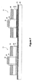
図7は、本発明の実施形態により形成された第1SOI・MOSFETと第2SOI・MOSFETからなるCMOSデバイスの素子の一例を示す図である。
この構造では、n型MOSFETデバイス70に、基板の絶縁層52上に形成される半導体領域72が組み入れられている。この半導体領域72は、絶縁層52の有効な格子定数よりも低い格子定数を有しており、半導体領域72に引張歪みを与えるとともにn型MOSFET中の電子の移動度を増加させることになる、第1シリコンゲルマニウム合金からできている。
この構造はさらに、基板の絶縁層52上に形成される半導体領域76を組み入れられたp型のMOSFETデバイス74を含んでいる。
この半導体領域76は、絶縁層52の有効な格子定数よりも大きい格子定数を有しており、半導体領域76に圧縮歪みを与えるとともにp型MOSFET中のホールの移動度を増加させることになる、第2シリコンゲルマニウム合金からできている。
n型MOSFETおよびp型MOSFETは、絶縁層によって、これらに異なる種類の歪みが与えられる、異なるシリコンゲルマニウム合金を使用することにより、各デバイスのキャリア移動度が増加するという利点を得ることができる、CMOSデバイスを形成するように接続することができる。
FIG. 7 is a diagram showing an example of a CMOS device element composed of a first SOI MOSFET and a second SOI MOSFET formed according to an embodiment of the present invention.
In this structure, the n-
The structure further includes a p-
The semiconductor region 76 has a lattice constant larger than the effective lattice constant of the insulating
n-type MOSFETs and p-type MOSFETs can have the advantage of increasing the carrier mobility of each device by using different silicon germanium alloys, which are given different types of strain by the insulating layer, Connections can be made to form CMOS devices.
図7の構造は、様々な方法により製造することができる。
例えば、p型デバイスおよびn型デバイスのそれぞれについての、異なる格子定数を有する半導体領域を成長させるのに、2つの独立した成長ステップを実行することができる。
これらの領域は、デバイス中で利用されるであろう形状に成長させてもよいし、またはこれらの領域を正確な寸法にパターン化してもよい。
他の実施形態においては、合金のうちの1つの層をウェーハにわたり成長させることができる。その後、シリコンまたはゲルマニウムを選択した領域に注入してこれらの領域の理論混合比を変更し、第2合金を形成してもよい。
The structure of FIG. 7 can be manufactured by various methods.
For example, two independent growth steps can be performed to grow semiconductor regions having different lattice constants for each of a p-type device and an n-type device.
These regions may be grown to shapes that will be utilized in the device, or these regions may be patterned to exact dimensions.
In other embodiments, one layer of the alloy can be grown across the wafer. Thereafter, silicon or germanium may be injected into selected regions to change the theoretical mixing ratio of these regions to form the second alloy.
図7の構造は、nMOSおよびpMOSデバイスについて異なる種類の歪みを生成すべく、2つの異なるシリコンゲルマニウム合金を利用しているが、他の実施例においては、適当な格子定数を有する異なる種類の半導体材料が利用され得る。
さらに、絶縁材料の格子特性は、歪みを方向づけるように形成されてよい。
MOSFETは、図7に示す方法または他の様々な方法で形成することができる。
The structure of FIG. 7 utilizes two different silicon germanium alloys to generate different types of strain for nMOS and pMOS devices, but in other embodiments, different types of semiconductors with appropriate lattice constants. Materials can be utilized.
Further, the lattice properties of the insulating material may be formed to direct strain.
The MOSFET can be formed by the method shown in FIG. 7 or various other methods.
上記のプロセスにおいて記載したタスクは、他のタスクを除外するものではない。また、形成されるべき特定の構造により、上述のプロセスにさらなるタスクが組み入れられ得る。例えば、処理タスク間における不動態層または保護材料の形成または除去、フォトレジストマスクおよび他のマスキング層の形成または除去のような中間の処理タスク、ドーピングおよびカウンタドーピング、クリーニング、プレーナ化、および他のタスクを、特に上述したタスクと共に実行することができる。さらに、ウェーハ全体のような基板全面上においてここで記載したプロセスを実行する必要がないが、その代わりに基板の部分上で選択的に実行することができる。さらに、例示のため、ここに記載した構造の製造の間、ある特定の順番にタスクを実行するように記載したが、実施形態によっては、プロセスの目的を達成する他の順番でタスクを実行することができる。このように、図示した上述の実施形態が現在の好ましい一例である一方、これらの実施形態は単なる例示としての記載であることを理解すべきである。本発明は特定の実施形態に制限されず、請求の範囲およびこの等価物の範囲内の、様々な変形例、組合せおよび置換に及ぶ。 The tasks described in the above process do not exclude other tasks. Also, depending on the particular structure to be formed, additional tasks can be incorporated into the above-described process. For example, intermediate processing tasks such as formation or removal of passivation layers or protective materials between processing tasks, formation or removal of photoresist masks and other masking layers, doping and counter-doping, cleaning, planarization, and other Tasks can be performed in particular with the tasks described above. Further, the process described herein need not be performed on the entire surface of the substrate, such as the entire wafer, but can instead be selectively performed on portions of the substrate. Further, for purposes of illustration, it has been described that the tasks are performed in a certain order during the manufacture of the structures described herein, but in some embodiments, the tasks are performed in other orders that achieve the purpose of the process. be able to. Thus, while the illustrated embodiments described above are presently preferred examples, it should be understood that these embodiments are merely exemplary descriptions. The invention is not limited to the specific embodiments, but extends to various modifications, combinations and substitutions within the scope of the claims and their equivalents.
Claims (10)
前記絶縁層上に形成される半導体材料の層(54)と、
そのチャネル領域中に半導体材料の層が組み入れられるMOSFETと、を含む、
SOI(semiconductor on insulator)デバイス。 A substrate comprising a layer (52) of insulating material having a perovskite lattice;
A layer (54) of semiconductor material formed on the insulating layer;
A MOSFET in which a layer of semiconductor material is incorporated in its channel region,
SOI (semiconductor on insulator) device.
前記絶縁材料(52)の前記ペロブスカイト格子の(001)面上に、ダイヤモンド型格子を有する半導体材料の層(54)を成長させ、
そのチャネル領域中に、前記半導体材料(54)を組み入れたMOSFETを形成する、
SOI(semiconductor on insulator)MOSFETデバイス上に半導体を形成する方法。 Forming a substrate comprising a layer of insulating material (52) having a perovskite lattice;
A layer (54) of semiconductor material having a diamond-type lattice is grown on the (001) plane of the perovskite lattice of the insulating material (52);
Forming a MOSFET incorporating said semiconductor material (54) in its channel region;
A method of forming a semiconductor on an SOI (semiconductor on insulator) MOSFET device.
前記絶縁層(52)上に形成される第1半導体材料(72)の領域であって、前記絶縁層(52)により引っ張り歪みが与えられる第1半導体材料(72)の領域と、
前記第1半導体材料(72)の領域中に形成され、そのチャネル領域中に、前記第1半導体材料を組み入れる、第1MOSFET(70)と、
前記絶縁材料の層(52)上に形成される第2半導体材料(76)の領域であって、前記絶縁層により圧縮歪みが与えられる第1半導体材料(76)の領域と、
前記第2半導体材料(76)の領域中に形成され、そのチャネル領域中に、前記第2半導体材料を組み入れる、第2MOSFET(74)と、を含む、
SOI(semiconductor on insulator)デバイス。 A substrate comprising a layer (52) of insulating material having a perovskite lattice;
A region of the first semiconductor material (72) formed on the insulating layer (52), the region of the first semiconductor material (72) being subjected to tensile strain by the insulating layer (52);
A first MOSFET (70) formed in a region of the first semiconductor material (72) and incorporating the first semiconductor material in a channel region thereof;
A region of the second semiconductor material (76) formed on the layer (52) of insulating material, the region of the first semiconductor material (76) being subjected to compressive strain by the insulating layer;
A second MOSFET (74) formed in the region of the second semiconductor material (76) and incorporating the second semiconductor material in its channel region;
SOI (semiconductor on insulator) device.
前記第2半導体材料(76)は、前記絶縁材料(52)の有効な格子定数より大きい格子定数を有するシリコンゲルマニウム合金である、請求項8記載のデバイス。 The first semiconductor material (72) is a silicon germanium alloy having a lattice constant less than the effective lattice constant of the insulating material (52);
The device of claim 8, wherein the second semiconductor material (76) is a silicon germanium alloy having a lattice constant greater than the effective lattice constant of the insulating material (52).
Applications Claiming Priority (2)
| Application Number | Priority Date | Filing Date | Title |
|---|---|---|---|
| US10/819,441 US7005302B2 (en) | 2004-04-07 | 2004-04-07 | Semiconductor on insulator substrate and devices formed therefrom |
| PCT/US2005/010574 WO2005101521A1 (en) | 2004-04-07 | 2005-03-28 | Semiconductor on insulator substrate and devices formed therefrom |
Publications (2)
| Publication Number | Publication Date |
|---|---|
| JP2007533137A true JP2007533137A (en) | 2007-11-15 |
| JP2007533137A5 JP2007533137A5 (en) | 2008-05-15 |
Family
ID=34964796
Family Applications (1)
| Application Number | Title | Priority Date | Filing Date |
|---|---|---|---|
| JP2007507361A Pending JP2007533137A (en) | 2004-04-07 | 2005-03-28 | SOI (Semiconductor Conductor Insulator) Substrate and Device Formed from This Substrate |
Country Status (8)
| Country | Link |
|---|---|
| US (2) | US7005302B2 (en) |
| JP (1) | JP2007533137A (en) |
| KR (1) | KR101093785B1 (en) |
| CN (1) | CN1998088B (en) |
| DE (1) | DE112005000775B4 (en) |
| GB (1) | GB2429114B (en) |
| TW (1) | TWI360833B (en) |
| WO (1) | WO2005101521A1 (en) |
Cited By (2)
| Publication number | Priority date | Publication date | Assignee | Title |
|---|---|---|---|---|
| JP2012186493A (en) * | 2012-05-14 | 2012-09-27 | Sony Corp | Semiconductor device |
| JP2013102203A (en) * | 2007-02-21 | 2013-05-23 | Internatl Business Mach Corp <Ibm> | Semiconductor structure including gate electrode having laterally variable work function |
Families Citing this family (19)
| Publication number | Priority date | Publication date | Assignee | Title |
|---|---|---|---|---|
| US7365357B2 (en) * | 2005-07-22 | 2008-04-29 | Translucent Inc. | Strain inducing multi-layer cap |
| US7202513B1 (en) * | 2005-09-29 | 2007-04-10 | International Business Machines Corporation | Stress engineering using dual pad nitride with selective SOI device architecture |
| US7495290B2 (en) * | 2005-12-14 | 2009-02-24 | Infineon Technologies Ag | Semiconductor devices and methods of manufacture thereof |
| KR100649874B1 (en) * | 2005-12-29 | 2006-11-27 | 동부일렉트로닉스 주식회사 | Method for fabricating transistor by using soi wafer |
| DE102006035669B4 (en) * | 2006-07-31 | 2014-07-10 | Globalfoundries Inc. | Transistor having a deformed channel region having a performance enhancing material composition and methods of manufacture |
| KR100850899B1 (en) * | 2007-02-09 | 2008-08-07 | 엘지전자 주식회사 | Thin film transistot and fabrication method of the same |
| KR100994995B1 (en) * | 2007-08-07 | 2010-11-18 | 삼성전자주식회사 | Semiconductor film stack containing DyScO3 film and method for formation of the same |
| US7692224B2 (en) * | 2007-09-28 | 2010-04-06 | Freescale Semiconductor, Inc. | MOSFET structure and method of manufacture |
| JP5190275B2 (en) * | 2008-01-09 | 2013-04-24 | パナソニック株式会社 | Semiconductor memory cell and semiconductor memory array using the same |
| KR101535222B1 (en) * | 2008-04-17 | 2015-07-08 | 삼성전자주식회사 | Semiconductor device and method of fabricating the same |
| US8835955B2 (en) * | 2010-11-01 | 2014-09-16 | Translucent, Inc. | IIIOxNy on single crystal SOI substrate and III n growth platform |
| CN102751231A (en) * | 2012-03-13 | 2012-10-24 | 清华大学 | Semiconductor structure and forming method thereof |
| CN102683345B (en) * | 2012-05-22 | 2015-04-15 | 清华大学 | Semiconductor structure and forming method thereof |
| CN102683388B (en) * | 2012-05-30 | 2016-06-29 | 清华大学 | Semiconductor structure and forming method thereof |
| CN102903739B (en) * | 2012-10-19 | 2016-01-20 | 清华大学 | There is the semiconductor structure of rare earth oxide |
| CN102916039B (en) * | 2012-10-19 | 2016-01-20 | 清华大学 | There is the semiconductor structure of beryllium oxide |
| US9570588B2 (en) * | 2014-12-29 | 2017-02-14 | Globalfoundries Inc. | Methods of forming transistor structures including forming channel material after formation processes to prevent damage to the channel material |
| CN108060457A (en) * | 2017-12-21 | 2018-05-22 | 苏州晶享嘉世光电科技有限公司 | A kind of scandium acid gadolinium yttrium crystal and crystal growth method by melt method |
| CN110284192A (en) * | 2019-06-17 | 2019-09-27 | 南京同溧晶体材料研究院有限公司 | Infrared band laser crystal and preparation method thereof in 3 μm of er-doped scandium acid gadolinium a kind of |
Citations (3)
| Publication number | Priority date | Publication date | Assignee | Title |
|---|---|---|---|---|
| JPH09219524A (en) * | 1996-02-09 | 1997-08-19 | Toshiba Corp | Semiconductor device and its manufacture |
| JP2001110801A (en) * | 1999-10-05 | 2001-04-20 | Takeshi Yao | Pattern formation method, electronic element, optical element, and circuit substrate |
| JP2003303971A (en) * | 2002-04-09 | 2003-10-24 | Matsushita Electric Ind Co Ltd | Semiconductor substrate and semiconductor device |
Family Cites Families (11)
| Publication number | Priority date | Publication date | Assignee | Title |
|---|---|---|---|---|
| US5830270A (en) * | 1996-08-05 | 1998-11-03 | Lockheed Martin Energy Systems, Inc. | CaTiO3 Interfacial template structure on semiconductor-based material and the growth of electroceramic thin-films in the perovskite class |
| US6603156B2 (en) | 2001-03-31 | 2003-08-05 | International Business Machines Corporation | Strained silicon on insulator structures |
| US20020195599A1 (en) | 2001-06-20 | 2002-12-26 | Motorola, Inc. | Low-defect semiconductor structure, device including the structure and method for fabricating structure and device |
| US6933566B2 (en) | 2001-07-05 | 2005-08-23 | International Business Machines Corporation | Method of forming lattice-matched structure on silicon and structure formed thereby |
| US20030020070A1 (en) * | 2001-07-25 | 2003-01-30 | Motorola, Inc. | Semiconductor structure for isolating high frequency circuitry and method for fabricating |
| US6589856B2 (en) | 2001-08-06 | 2003-07-08 | Motorola, Inc. | Method and apparatus for controlling anti-phase domains in semiconductor structures and devices |
| JP4090716B2 (en) | 2001-09-10 | 2008-05-28 | 雅司 川崎 | Thin film transistor and matrix display device |
| JP4034627B2 (en) * | 2001-09-28 | 2008-01-16 | テキサス インスツルメンツ インコーポレイテツド | Integrated circuit and manufacturing method thereof |
| US6717216B1 (en) * | 2002-12-12 | 2004-04-06 | International Business Machines Corporation | SOI based field effect transistor having a compressive film in undercut area under the channel and a method of making the device |
| US6730576B1 (en) | 2002-12-31 | 2004-05-04 | Advanced Micro Devices, Inc. | Method of forming a thick strained silicon layer and semiconductor structures incorporating a thick strained silicon layer |
| US6803631B2 (en) | 2003-01-23 | 2004-10-12 | Advanced Micro Devices, Inc. | Strained channel finfet |
-
2004
- 2004-04-07 US US10/819,441 patent/US7005302B2/en not_active Expired - Lifetime
-
2005
- 2005-03-28 DE DE112005000775T patent/DE112005000775B4/en not_active Expired - Fee Related
- 2005-03-28 KR KR1020067023279A patent/KR101093785B1/en not_active IP Right Cessation
- 2005-03-28 GB GB0619840A patent/GB2429114B/en not_active Expired - Fee Related
- 2005-03-28 CN CN2005800183302A patent/CN1998088B/en not_active Expired - Fee Related
- 2005-03-28 WO PCT/US2005/010574 patent/WO2005101521A1/en active Application Filing
- 2005-03-28 JP JP2007507361A patent/JP2007533137A/en active Pending
- 2005-04-04 TW TW094110692A patent/TWI360833B/en not_active IP Right Cessation
-
2006
- 2006-02-24 US US11/361,207 patent/US7221025B2/en not_active Expired - Lifetime
Patent Citations (3)
| Publication number | Priority date | Publication date | Assignee | Title |
|---|---|---|---|---|
| JPH09219524A (en) * | 1996-02-09 | 1997-08-19 | Toshiba Corp | Semiconductor device and its manufacture |
| JP2001110801A (en) * | 1999-10-05 | 2001-04-20 | Takeshi Yao | Pattern formation method, electronic element, optical element, and circuit substrate |
| JP2003303971A (en) * | 2002-04-09 | 2003-10-24 | Matsushita Electric Ind Co Ltd | Semiconductor substrate and semiconductor device |
Cited By (2)
| Publication number | Priority date | Publication date | Assignee | Title |
|---|---|---|---|---|
| JP2013102203A (en) * | 2007-02-21 | 2013-05-23 | Internatl Business Mach Corp <Ibm> | Semiconductor structure including gate electrode having laterally variable work function |
| JP2012186493A (en) * | 2012-05-14 | 2012-09-27 | Sony Corp | Semiconductor device |
Also Published As
| Publication number | Publication date |
|---|---|
| KR20070012458A (en) | 2007-01-25 |
| US20050224879A1 (en) | 2005-10-13 |
| GB2429114B (en) | 2009-04-01 |
| TWI360833B (en) | 2012-03-21 |
| TW200539278A (en) | 2005-12-01 |
| US20060138542A1 (en) | 2006-06-29 |
| CN1998088A (en) | 2007-07-11 |
| GB2429114A (en) | 2007-02-14 |
| KR101093785B1 (en) | 2011-12-19 |
| US7221025B2 (en) | 2007-05-22 |
| DE112005000775T5 (en) | 2007-05-31 |
| CN1998088B (en) | 2010-08-25 |
| DE112005000775B4 (en) | 2012-10-31 |
| GB0619840D0 (en) | 2006-11-29 |
| WO2005101521A1 (en) | 2005-10-27 |
| US7005302B2 (en) | 2006-02-28 |
Similar Documents
| Publication | Publication Date | Title |
|---|---|---|
| US7221025B2 (en) | Semiconductor on insulator substrate and devices formed therefrom | |
| US6800910B2 (en) | FinFET device incorporating strained silicon in the channel region | |
| US7701019B2 (en) | Tensile strained substrate | |
| US6852600B1 (en) | Strained silicon MOSFET having silicon source/drain regions and method for its fabrication | |
| US11705517B2 (en) | Nanosheet transistors with strained channel regions | |
| US7071065B1 (en) | Strained silicon PMOS having silicon germanium source/drain extensions and method for its fabrication | |
| US7547641B2 (en) | Super hybrid SOI CMOS devices | |
| US8946063B2 (en) | Semiconductor device having SSOI substrate with relaxed tensile stress | |
| US20050040444A1 (en) | Strained-channel fin field effect transistor (FET) with a uniform channel thickness and separate gates | |
| TWI387010B (en) | Method for fabricating a transistor | |
| KR20090094018A (en) | Semiconductor device and process for producing the same | |
| JP2012089784A (en) | Semiconductor device and method for manufacturing the same | |
| CN112635391B (en) | Strained germanium tin silicon substrate on insulator, transistor and preparation method thereof | |
| JP2010206097A (en) | Semiconductor element, and semiconductor device | |
| JP2008159960A (en) | Manufacturing method of semiconductor device | |
| US9263584B2 (en) | Field effect transistors employing a thin channel region on a crystalline insulator structure | |
| US11646238B2 (en) | Dual crystal orientation for semiconductor devices | |
| CN113745220A (en) | Semiconductor device and method of forming the same | |
| JP4290038B2 (en) | Semiconductor device, transistor, and manufacturing method of semiconductor device | |
| TWI670775B (en) | Semiconductor device structures and methods for manufacturing the same | |
| US20220328650A1 (en) | Metal gates and methods of forming the same |
Legal Events
| Date | Code | Title | Description |
|---|---|---|---|
| A521 | Written amendment |
Free format text: JAPANESE INTERMEDIATE CODE: A523 Effective date: 20080328 |
|
| A621 | Written request for application examination |
Free format text: JAPANESE INTERMEDIATE CODE: A621 Effective date: 20080328 |
|
| RD03 | Notification of appointment of power of attorney |
Free format text: JAPANESE INTERMEDIATE CODE: A7423 Effective date: 20100421 |
|
| RD05 | Notification of revocation of power of attorney |
Free format text: JAPANESE INTERMEDIATE CODE: A7425 Effective date: 20100902 |
|
| A977 | Report on retrieval |
Free format text: JAPANESE INTERMEDIATE CODE: A971007 Effective date: 20111024 |
|
| A131 | Notification of reasons for refusal |
Free format text: JAPANESE INTERMEDIATE CODE: A131 Effective date: 20111102 |
|
| A02 | Decision of refusal |
Free format text: JAPANESE INTERMEDIATE CODE: A02 Effective date: 20120328 |