JP2007523563A - Magnetic field shaping shielding for radio frequency identification (RFID) systems - Google Patents
Magnetic field shaping shielding for radio frequency identification (RFID) systems Download PDFInfo
- Publication number
- JP2007523563A JP2007523563A JP2006554090A JP2006554090A JP2007523563A JP 2007523563 A JP2007523563 A JP 2007523563A JP 2006554090 A JP2006554090 A JP 2006554090A JP 2006554090 A JP2006554090 A JP 2006554090A JP 2007523563 A JP2007523563 A JP 2007523563A
- Authority
- JP
- Japan
- Prior art keywords
- antenna
- rfid
- conductive
- rfid system
- conductive shield
- Prior art date
- Legal status (The legal status is an assumption and is not a legal conclusion. Google has not performed a legal analysis and makes no representation as to the accuracy of the status listed.)
- Pending
Links
Images


Classifications
-
- H—ELECTRICITY
- H01—ELECTRIC ELEMENTS
- H01Q—ANTENNAS, i.e. RADIO AERIALS
- H01Q1/00—Details of, or arrangements associated with, antennas
- H01Q1/12—Supports; Mounting means
- H01Q1/22—Supports; Mounting means by structural association with other equipment or articles
- H01Q1/24—Supports; Mounting means by structural association with other equipment or articles with receiving set
-
- H—ELECTRICITY
- H01—ELECTRIC ELEMENTS
- H01Q—ANTENNAS, i.e. RADIO AERIALS
- H01Q1/00—Details of, or arrangements associated with, antennas
- H01Q1/12—Supports; Mounting means
- H01Q1/22—Supports; Mounting means by structural association with other equipment or articles
- H01Q1/2208—Supports; Mounting means by structural association with other equipment or articles associated with components used in interrogation type services, i.e. in systems for information exchange between an interrogator/reader and a tag/transponder, e.g. in Radio Frequency Identification [RFID] systems
-
- G—PHYSICS
- G06—COMPUTING; CALCULATING OR COUNTING
- G06K—GRAPHICAL DATA READING; PRESENTATION OF DATA; RECORD CARRIERS; HANDLING RECORD CARRIERS
- G06K17/00—Methods or arrangements for effecting co-operative working between equipments covered by two or more of main groups G06K1/00 - G06K15/00, e.g. automatic card files incorporating conveying and reading operations
-
- G—PHYSICS
- G06—COMPUTING; CALCULATING OR COUNTING
- G06K—GRAPHICAL DATA READING; PRESENTATION OF DATA; RECORD CARRIERS; HANDLING RECORD CARRIERS
- G06K19/00—Record carriers for use with machines and with at least a part designed to carry digital markings
- G06K19/06—Record carriers for use with machines and with at least a part designed to carry digital markings characterised by the kind of the digital marking, e.g. shape, nature, code
- G06K19/067—Record carriers with conductive marks, printed circuits or semiconductor circuit elements, e.g. credit or identity cards also with resonating or responding marks without active components
- G06K19/07—Record carriers with conductive marks, printed circuits or semiconductor circuit elements, e.g. credit or identity cards also with resonating or responding marks without active components with integrated circuit chips
-
- G—PHYSICS
- G06—COMPUTING; CALCULATING OR COUNTING
- G06K—GRAPHICAL DATA READING; PRESENTATION OF DATA; RECORD CARRIERS; HANDLING RECORD CARRIERS
- G06K7/00—Methods or arrangements for sensing record carriers, e.g. for reading patterns
- G06K7/10—Methods or arrangements for sensing record carriers, e.g. for reading patterns by electromagnetic radiation, e.g. optical sensing; by corpuscular radiation
- G06K7/10009—Methods or arrangements for sensing record carriers, e.g. for reading patterns by electromagnetic radiation, e.g. optical sensing; by corpuscular radiation sensing by radiation using wavelengths larger than 0.1 mm, e.g. radio-waves or microwaves
- G06K7/10158—Methods or arrangements for sensing record carriers, e.g. for reading patterns by electromagnetic radiation, e.g. optical sensing; by corpuscular radiation sensing by radiation using wavelengths larger than 0.1 mm, e.g. radio-waves or microwaves methods and means used by the interrogation device for reliably powering the wireless record carriers using an electromagnetic interrogation field
- G06K7/10178—Methods or arrangements for sensing record carriers, e.g. for reading patterns by electromagnetic radiation, e.g. optical sensing; by corpuscular radiation sensing by radiation using wavelengths larger than 0.1 mm, e.g. radio-waves or microwaves methods and means used by the interrogation device for reliably powering the wireless record carriers using an electromagnetic interrogation field including auxiliary means for focusing, repeating or boosting the electromagnetic interrogation field
-
- G—PHYSICS
- G06—COMPUTING; CALCULATING OR COUNTING
- G06K—GRAPHICAL DATA READING; PRESENTATION OF DATA; RECORD CARRIERS; HANDLING RECORD CARRIERS
- G06K7/00—Methods or arrangements for sensing record carriers, e.g. for reading patterns
- G06K7/10—Methods or arrangements for sensing record carriers, e.g. for reading patterns by electromagnetic radiation, e.g. optical sensing; by corpuscular radiation
- G06K7/10009—Methods or arrangements for sensing record carriers, e.g. for reading patterns by electromagnetic radiation, e.g. optical sensing; by corpuscular radiation sensing by radiation using wavelengths larger than 0.1 mm, e.g. radio-waves or microwaves
- G06K7/10316—Methods or arrangements for sensing record carriers, e.g. for reading patterns by electromagnetic radiation, e.g. optical sensing; by corpuscular radiation sensing by radiation using wavelengths larger than 0.1 mm, e.g. radio-waves or microwaves using at least one antenna particularly designed for interrogating the wireless record carriers
- G06K7/10336—Methods or arrangements for sensing record carriers, e.g. for reading patterns by electromagnetic radiation, e.g. optical sensing; by corpuscular radiation sensing by radiation using wavelengths larger than 0.1 mm, e.g. radio-waves or microwaves using at least one antenna particularly designed for interrogating the wireless record carriers the antenna being of the near field type, inductive coil
-
- G—PHYSICS
- G06—COMPUTING; CALCULATING OR COUNTING
- G06K—GRAPHICAL DATA READING; PRESENTATION OF DATA; RECORD CARRIERS; HANDLING RECORD CARRIERS
- G06K7/00—Methods or arrangements for sensing record carriers, e.g. for reading patterns
- G06K7/10—Methods or arrangements for sensing record carriers, e.g. for reading patterns by electromagnetic radiation, e.g. optical sensing; by corpuscular radiation
- G06K7/10009—Methods or arrangements for sensing record carriers, e.g. for reading patterns by electromagnetic radiation, e.g. optical sensing; by corpuscular radiation sensing by radiation using wavelengths larger than 0.1 mm, e.g. radio-waves or microwaves
- G06K7/10316—Methods or arrangements for sensing record carriers, e.g. for reading patterns by electromagnetic radiation, e.g. optical sensing; by corpuscular radiation sensing by radiation using wavelengths larger than 0.1 mm, e.g. radio-waves or microwaves using at least one antenna particularly designed for interrogating the wireless record carriers
- G06K7/10346—Methods or arrangements for sensing record carriers, e.g. for reading patterns by electromagnetic radiation, e.g. optical sensing; by corpuscular radiation sensing by radiation using wavelengths larger than 0.1 mm, e.g. radio-waves or microwaves using at least one antenna particularly designed for interrogating the wireless record carriers the antenna being of the far field type, e.g. HF types or dipoles
-
- H—ELECTRICITY
- H01—ELECTRIC ELEMENTS
- H01Q—ANTENNAS, i.e. RADIO AERIALS
- H01Q1/00—Details of, or arrangements associated with, antennas
- H01Q1/12—Supports; Mounting means
- H01Q1/22—Supports; Mounting means by structural association with other equipment or articles
-
- H—ELECTRICITY
- H01—ELECTRIC ELEMENTS
- H01Q—ANTENNAS, i.e. RADIO AERIALS
- H01Q1/00—Details of, or arrangements associated with, antennas
- H01Q1/52—Means for reducing coupling between antennas; Means for reducing coupling between an antenna and another structure
- H01Q1/526—Electromagnetic shields
-
- H—ELECTRICITY
- H01—ELECTRIC ELEMENTS
- H01Q—ANTENNAS, i.e. RADIO AERIALS
- H01Q7/00—Loop antennas with a substantially uniform current distribution around the loop and having a directional radiation pattern in a plane perpendicular to the plane of the loop
Abstract
無線識別(RFID)タグとの通信用のアンテナにより形成された電磁界を整形するために、実質的に連続する導電性シールドを用いるRFIDシステムが記載されている。アンテナと導電性シールドとは実質的に平面形状を有し、返却/貸出領域の表面に載置し得る。導電性シールドは、アンテナの周囲であってアンテナに平行な面、例えば同一平面内に位置決めされている。導電性シールドは電磁界を整形してアンテナに対して実質的に垂直方向に延びるようにするとともに、電磁界が実質的に導電性シールド上方に生じるのを防止する。 An RFID system is described that uses a substantially continuous conductive shield to shape the electromagnetic field formed by an antenna for communication with a radio frequency identification (RFID) tag. The antenna and the conductive shield have a substantially planar shape and can be placed on the surface of the return / rental area. The conductive shield is positioned around the antenna and parallel to the antenna, for example, in the same plane. The conductive shield shapes the electromagnetic field so that it extends substantially perpendicular to the antenna and prevents the electromagnetic field from occurring substantially above the conductive shield.
Description
本発明は物品管理用無線識別(RFID)システムに関する。 The present invention relates to a radio frequency identification (RFID) system for article management.
無線識別(RFID)技術は、輸送、製造、廃棄物管理、郵便追跡、航空機荷物調整、および高速道路通行料金管理を始めとする殆どすべての産業界で広く用いられてきている。典型的なRFIDシステムは、複数のRFIDタグと、RFIDタグと通信するアンテナを有する少なくとも1つのRFIDリーダまたは検出システムと、RFIDリーダを制御する計算装置とを含んでいる。RFIDリーダは、タグにエネルギーまたは情報を提供し得る送信器と、タグから識別情報(identity)および他の情報を受信する受信器とを含んでいる。計算装置はRFIDリーダによって得た情報を処理する。 Radio frequency identification (RFID) technology has been widely used in almost every industry, including transportation, manufacturing, waste management, postal tracking, aircraft luggage adjustment, and highway toll management. A typical RFID system includes a plurality of RFID tags, at least one RFID reader or detection system having an antenna in communication with the RFID tags, and a computing device that controls the RFID reader. An RFID reader includes a transmitter that can provide energy or information to the tag, and a receiver that receives identity and other information from the tag. The computing device processes the information obtained by the RFID reader.
一般に、RFIDタグから受信した情報は特定の用途に特有であるが、タグが取り付けられた物品の識別を提供することが多い。好例となる物品には製造物、本、ファイル、動物または個人、もしくは殆どの任意の他の実在物品がある。物品に対して追加情報も提供し得る。タグを製造工程中に用いて、例えば製造中の自動車のシャーシの塗料の色または他の有用な情報を示し得る。 In general, information received from an RFID tag is specific to a particular application, but often provides identification of the item to which the tag is attached. Exemplary articles include manufactured goods, books, files, animals or individuals, or almost any other real article. Additional information may also be provided for the article. The tag may be used during the manufacturing process to indicate, for example, paint color or other useful information on the automobile chassis being manufactured.
RFIDリーダの送信器はアンテナを通してRF信号を出力して磁界を生成し、その磁界によりタグは情報を担持するRF信号を返すことができる。いくつかの構成では送信器は通信を開始するとともに、増幅器を利用してアンテナを変調出力信号で駆動し、RFIDタグと通信する。他の構成では、RFIDタグはRFIDリーダから連続波信号を受信するとともに、その情報に即座に応答することにより通信を開始する。 The transmitter of the RFID reader outputs an RF signal through the antenna to generate a magnetic field that allows the tag to return an RF signal carrying information. In some configurations, the transmitter initiates communication and utilizes an amplifier to drive the antenna with the modulated output signal to communicate with the RFID tag. In another configuration, the RFID tag receives a continuous wave signal from the RFID reader and initiates communication by responding immediately to the information.
従来のタグは、内部電源を含む「能動」タグ、またはRFIDリーダにより生成された磁界により励磁される「受動」タグであり得る。いずれの場合もタグが事前規定されたプロトコルを用いて通信することにより、RFIDリーダは、1つまたは複数のタグから情報を受信することができる。計算装置はRFIDリーダからの情報を受け取るとともに、データベースを更新するなどの、ある動作を行うことにより情報管理システムとして機能する。さらに計算装置は、送信器を介してタグにデータを伝播する機構として機能し得る。 A conventional tag can be an “active” tag that includes an internal power supply, or a “passive” tag that is excited by a magnetic field generated by an RFID reader. In either case, the RFID reader can receive information from one or more tags by the tags communicating using a predefined protocol. The computing device receives information from the RFID reader and functions as an information management system by performing certain operations such as updating a database. Further, the computing device can function as a mechanism for propagating data to the tag via the transmitter.
RFIDリーダ用の従来のアンテナは、単一の誘電ループを有して比較的高い周波数範囲、例えば3メガヘルツ(MHz)〜30MHzで動作する。その結果、これらのアンテナは「ホール」、すなわちRFIDタグをアンテナの比較的近くに配置しても、RFIDタグが読み取ることができない領域のある磁界を生成しやすい。例えば、RFIDタグが取り付けられた物品の配向および場所に拠って、ある状況では、RFIDタグは問い合わせ時にアンテナの誘電ループの単一巻の上方に中心が位置し得る。この状況では、実質的に等しい電流がRFIDタグの両側に印加される場合があり、相殺作用をもたらす。その結果、RFIDタグはリーダとのRFID通信を達成することができない虞がある。 Conventional antennas for RFID readers have a single dielectric loop and operate in a relatively high frequency range, for example, 3 megahertz (MHz) to 30 MHz. As a result, these antennas tend to generate “holes”, that is, magnetic fields with areas that the RFID tags cannot read even if the RFID tag is placed relatively close to the antenna. For example, depending on the orientation and location of the article to which the RFID tag is attached, in some situations, the RFID tag may be centered over a single turn of the antenna's dielectric loop when interrogated. In this situation, substantially equal currents may be applied to both sides of the RFID tag, resulting in an offset effect. As a result, the RFID tag may not be able to achieve RFID communication with the reader.
さらに、卓上型RFIDリーダと共に用いられる従来のアンテナは、アンテナの周縁部を超えて水平に延びる磁界を生成しやすい。従ってアンテナ付近、例えば卓上でアンテナの隣に配置された物品は、リーダによって不用意に読み取られる場合があり、これは望ましくない結果をもたらす虞がある。例えば、1人の図書館利用者が所持するとともに、図書館管理システムのアンテナの隣に置かれた本が、他の利用者へ不用意に貸し出される場合がある。 Furthermore, conventional antennas used with desktop RFID readers tend to generate a magnetic field that extends horizontally beyond the periphery of the antenna. Thus, articles placed near the antenna, for example, on the desk next to the antenna, may be inadvertently read by the reader, which can have undesirable results. For example, a book owned by one library user and a book placed next to the antenna of the library management system may be inadvertently lent to another user.
磁界をRFIDシステムで用いる所望の構成に整形する磁界整形アンテナ、および遮蔽構成要素の概要を説明する。特に、ループが合成磁界内のホールのサイズを低減するように位置決めされるとともに、離間している双ループアンテナを説明する。さらに、上記の双ループアンテナの構成は、同等な電力で単一ループアンテナに対して磁界サイズの増加を達成するとともに、巻線間容量を低減することにより、アンテナにより達成される全体読み取り範囲を増大する。 An outline of a magnetic field shaping antenna for shaping a magnetic field into a desired configuration for use in an RFID system and shielding components will be described. In particular, a dual loop antenna is described in which the loops are positioned to reduce the size of the holes in the resultant magnetic field and are spaced apart. In addition, the dual loop antenna configuration described above achieves an increase in magnetic field size over a single loop antenna with comparable power and reduces the overall winding range achieved by the antenna by reducing the interwinding capacitance. Increase.
さらに、アンテナにより生成された磁界を、さらに精密化するとともに整形する導電性シールドを説明する。例えば、アンテナは、卓上またはカウンタトップ上に実質的に水平に位置決めできる。導電性シールドを、アンテナと同一平面内に配置する、および通常はアンテナを取り囲む等アンテナの面に平行に配向することにより、電磁界がアンテナの周縁部を超えて水平に延びる範囲を限定できる。その結果、アンテナのおおむね上方および下方に突出し、RFIDタグを読み取ることができる概して垂直通信ゾーンを規定する電磁界が生成される。 Further, a conductive shield that refines and shapes the magnetic field generated by the antenna will be described. For example, the antenna can be positioned substantially horizontally on a tabletop or countertop. By placing the conductive shield in the same plane as the antenna and orienting it parallel to the surface of the antenna, such as normally surrounding the antenna, the range in which the electromagnetic field extends horizontally beyond the periphery of the antenna can be limited. The result is an electromagnetic field that protrudes generally above and below the antenna and that defines a generally vertical communication zone from which the RFID tag can be read.
一実施形態において、多重ループアンテナは、無線識別(RFID)タグとのRFID通信用の電磁界を生成する複数の導電ループを備える。導電ループは少なくとも、アンテナが通信するRFIDタグの寸法に基づいて選択された距離離間している。 In one embodiment, the multi-loop antenna comprises a plurality of conductive loops that generate an electromagnetic field for RFID communication with a radio frequency identification (RFID) tag. The conductive loops are at least a selected distance apart based on the dimensions of the RFID tag with which the antenna communicates.
他の実施形態において、無線識別(RFID)システムは、物品と関連するRFIDタグと、RFIDタグとの通信用の電磁界を生成する複数の導電ループを有するアンテナとを備える。導電ループは少なくとも、RFIDタグの寸法に少なくとも部分的に基づいて選択された距離離間している。 In other embodiments, a radio frequency identification (RFID) system comprises an RFID tag associated with an article and an antenna having a plurality of conductive loops that generate electromagnetic fields for communication with the RFID tag. The conductive loops are at least a selected distance apart based at least in part on the dimensions of the RFID tag.
他の実施形態において、無線識別(RFID)システムはRFIDタグとの通信用の電磁界を形成するアンテナを備え、アンテナは実質的に平面形状を有する。実質的に連続する導電性シールドが、アンテナの周囲であってアンテナに平行な面内に位置決めされている。 In other embodiments, a radio frequency identification (RFID) system includes an antenna that forms an electromagnetic field for communication with an RFID tag, the antenna having a substantially planar shape. A substantially continuous conductive shield is positioned in a plane around the antenna and parallel to the antenna.
本発明の1つまたは複数の実施形態の詳細が添付の図面および以下の説明に記載されている。本発明の他の特徴、目的及び利点は、明細書の記述と図面とから、さらには特許請求の範囲から明らかになろう。 The details of one or more embodiments of the invention are set forth in the accompanying drawings and the description below. Other features, objects, and advantages of the invention will be apparent from the description and drawings, and from the claims.
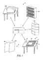
図1は本明細書に説明する技術を組み込んだ好的なRFIDシステム2を図示するブロック図である。図1の図示例においては、RFIDシステム2は、本、書類、ファイルまたは他の物品を追跡するのに使用されている。RFIDシステムは、例えば図書館、法律事務所、政府機関、または事業、犯罪および医療記録などの書類およびファイルを作製および/または保管する他の施設に配備され得る。これらの物品は物品を一意に識別するRFIDタグを含む。さらに、各RFIDタグは物品を説明する情報、物品の移動が許可されているか否かを示す状況情報も含む。RFIDタグをタグが実質的に感知されないように物品内に埋め込むことにより、改ざんを低減または防止し得る。
FIG. 1 is a block diagram illustrating a preferred
一般にRFIDシステム2は、±7kHzの許容周波数変動を有する13.56MHzなどの電磁スペクトルの周波数範囲内で動作する。しかし他の周波数をRFID用途に用い得るため、本発明はこれに限定されない。例えば、倉庫などの大型保管領域内のあるRFIDシステムは、およそ900MHzで動作するRFIDシステムを用い得る。
In general, the
図1に示すように、システム2は保護領域からの物品の不正移動を検出する退場制御システム5を含む。例えば、保護領域は図書館であり得るとともに、物品は一般に、図書館から貸し出しおよび返却される本または他の物品であり得る。本発明の範囲から逸脱することなく、この技術を他の種類の物品に適用することもできる。
As shown in FIG. 1, the
退場制御システム5は、保護領域の出口付近に位置する問い合わせゾーン、または通路を規定する格子9Aおよび9Bを含む。格子9Aおよび9Bは、RFIDタグが通路を通過する際にRFIDタグに問い合わせて、タグが取り付けられた品目の移動が許可されているか否かを判断するためのアンテナを含む。退場制御システム5は少なくとも1つのRFIDリーダ(図示せず)を用いてアンテナを駆動し得る。タグを検出するために、RFリーダはアンテナを介してRF電力を出力して問い合わせ通路内に電磁界を生成する。一般には、磁気構成要素を用いてRFIDタグと接続するため、本明細書では用語「電磁界」と「磁界」とは交換可能に用いられる。
The
RFリーダは問い合わせ通路内にある任意のタグから情報を受け取り、退場制御システム5は物品の移動が許可されているか否かを判定する。物品の移動が許可されていない場合には、退場制御システム5は所定の適切な保安動作、例えば可聴警報を鳴らす、出口ゲートをロックする等を開始する。
The RF reader receives information from an arbitrary tag in the inquiry path, and the
さらにRFIDシステム2は返却/貸出領域11を含み、それにより許可された人、例えば図書館利用者またはスタッフ人員は、物品を処理して移動または返却する。具体的には返却/貸出領域11は、物品に取り付けられたRFIDタグに問い合わせるとともに、それらの状況を所望のもの、例えば物品を返却または貸出に変更するRFIDリーダ18を含む。
Further, the
さらに物品を多数の保管領域12内、例えば図1に示すように開架12A、キャビネット12B、垂直ファイルセパレータ12C、または他の場所に位置決めし得る。各スマート保管領域12は施設中の物品の追跡を可能にするタグ問い合わせ能力を含む。例えば、図書館の環境では、返却後に開架12Aにある間、本を追跡することもできる。
Further, the articles may be positioned in a number of storage areas 12, such as in an
RFIDタグ自体は本発明の範囲から逸脱することなくかなり多数の形態を取り得る。市販のRFIDタグの例には、ミネソタ州セントポールのスリーエムカンパニー(3M Company,St.Paul,MN)から入手可能なスリーエム(登録商標)RFIDタグ、またはテキサス州ダラスのテキサス・インスツルメンツ(Texas Instruments,Dallas,TX)から入手可能な「タグ・イット(Tag−it)」RFIDトランスポンダがある。RFIDタグは通例、当該技術で周知の方法で電源からRFエネルギーを受け取るとともに、RFエネルギーを後方散乱するアンテナに動作的に接続された集積回路を含む。RFIDタグはRFエネルギーを変調して後方散乱信号を提供し、RFIDタグおよびその関連物品に関する情報を通信する。 The RFID tag itself can take many forms without departing from the scope of the present invention. Examples of commercially available RFID tags include 3M RFID tags available from 3M Company, St. Paul, Minn., Or Texas Instruments, Dallas, Texas. There is a “Tag-it” RFID transponder available from Dallas, TX). An RFID tag typically includes an integrated circuit that receives RF energy from a power source in a manner well known in the art and is operatively connected to an antenna that backscatters RF energy. The RFID tag modulates RF energy to provide a backscatter signal and communicates information about the RFID tag and its related items.
物品管理システム14は、施設内の物品毎にタグ情報の集中データベースを提供する。物品管理システム14はネットワーク化され、あるいは1つまたは複数のコンピュータに結合されて、様々な場所における司書などの個人が、それらの品目に関するデータにアクセスできるようになっている。例えば、ユーザは本などの特定の物品の場所および状況を要求し得る。物品管理システム14は、データベースから物品情報を検索するとともに、ユーザにスマート保管領域の1つ内で、その物品の場所が特定された最後の場所を報告し得る。状況に応じて、物品管理システム14は物品の現在の場所を再ポーリングあるいは再取得して、その物品がデータベース内で示された場所にあるということを確認することができる。
The
以下にさらに詳細に説明するように、RFIDシステム2は本明細書に記載する技術を組み込んでいる。返却/貸出領域11およびRFIDリーダ18は、例えば所望の構成で磁界を生成する磁界整形双ループアンテナ13と導電性シールド16とを組み込んでいる。例えば、RFIDリーダ18は、本明細書に説明する双ループアンテナ13を組み込み、生じる磁界内のホールのサイズを低減するようにループが位置決めされるとともに離間されている。これに加えて、上記の双ループアンテナ13の構成は、同等な電力で単一ループアンテナに対して磁界サイズの増加を達成するとともに、巻線間容量を低減することにより、RFIDリーダ18により達成される全体読み取り範囲を増大する。
As will be described in more detail below,
さらに返却/貸出領域11は、導電性シールド16を利用してアンテナ13により生成された磁界をさらに精密化および整形する。例えば、図示のようにアンテナ13を机面15上、内または下にほぼ水平に載置し得る。導電性シールド16をアンテナ13に平坦に且つ通常は取り囲むように配置して、電磁界がアンテナの周縁部を越えて水平に延びないようにする。その結果、通常はアンテナ13の上方および下方に突出し、RFIDタグを読み取ることができる、通常は垂直通信ゾーンを規定する電磁界が生成される。導電性シールド16を机面15上に、または図書館利用者および人員の視界外の机面の下方または内に載置し得る。導電性シールド16は本明細書に説明するように、磁界を形成するために必ずしも電気的に接地されている必要はない。
Further, the return /
図2はアンテナ13をさらに説明するブロック図である。図示のようにアンテナ13は一般に双ループ20を含み、双ループ20は以下にさらに詳細に説明するように、生じる磁界内のホールのサイズを減少させるとともに、磁界サイズおよび強度の増加を達成するように位置し、かつ離間している。一般に双ループを有するものとして説明するが、アンテナ13はタグ通信ゾーンの所望のサイズおよび個々のタグの寸法に基づいて、離間した追加のループを有してもよい。
FIG. 2 is a block diagram for further explaining the
同調回路22は双ループ20を共振周波数に同調させ、ループ構造と、同軸ケーブルであり得るケーブル26との間のインピーダンスの一致と信号変換とを提供する。リーダ18はケーブル26を介して同調回路22に結合されており、RFID送受信動作の両方にアンテナ13を利用する。従って、リーダ18は同調回路22から戻る信号を解釈する方向性結合器を含み得る。
The
図3は好的な双ループアンテナ30の平面図である。一つの好的な実施形態では、双ループ30はプリント回路基板の平行層上にある内側ループ32と外側ループ34とを含む。他の実施形態では内側ループ32と外側ループ34とは同一平面関係にある。
FIG. 3 is a plan view of a preferred
双ループ30の構成により、リーダ18(図1、2)からの電流(I)はループ32、34の各導電周縁部を通って同一方向に流れる。その結果、ループ32、34の平行導電周縁部により生成された電磁界は事実上付加的なものであり、同等の電力で単一ループアンテナに対して電磁界の大きさが増大した合成電磁界を達成する。
Due to the configuration of the
これに加えて、内側ループ32および外側ループ34は、合成磁界内の任意の潜在的ホールの数およびサイズを低減するように位置するとともに離間している。例えば、従来の単一ループアンテナとは異なり、リーダ18はアンテナの導電周縁部の真上に位置するRFIDタグとの良好な通信が達成可能であり得る。つまり、この状況では、従来の単一ループRFIDアンテナは実質的にRFIDタグの両側に等しい電流を生じさせ得るが、これが相殺効果につながる。これに対して、外側ループ34の周縁部の上方に中心が位置するRFIDタグは、例えば、内側ループ32のためRFIDタグの内側で電流の増加を達成することになる。同様に、内側ループ32の周縁部の上方に中心が位置するRFIDタグは、例えば、外側ループ34のためRFIDタグの外側で電流の増加を達成することになる。いずれの場合も電流の増加はRFIDタグ内のエネルギーの増加を達成し、それによりRFIDタグはRFIDリーダ18と良好に通信できる。このようにして、説明した双ループアンテナ30の構成は、合成電磁界内で任意のホールの数および/またはサイズを低減し得る。
In addition,
一実施形態において、内側ループ32および外側ループ34を少なくとも距離D離間して位置決めすることができる。ここで、Dはこのシステムで使用するRFIDタグの寸法に基づいて選択される。例えば、多数の従来の13.56MHzRFIDタグ用のサイズは、0.5インチ×1インチ(1.27cm×2.54cm)〜2インチ×3インチ(5.08cm×7.62cm)の寸法範囲である。このように、一実施形態においてRFIDタグの最大寸法を超えるようにDを選択して、RFIDタグが内側ループ32および外側ループ34の両方にまたがって位置できないようにすることができる。これは、タグの場所に関係なくタグとの良好な通信を達成するようにリーダ18の能力を向上するのに有利であろう。従って、一実施形態では、D≧2.54cmである。他の実施形態では、D≧5.08cmである。
In one embodiment, the
一般的な矩形の双ループに関して好的な目的で図示したが、円形、楕円形または他の幾何学的構成などの、他の形状のループを容易に用い得る。 Although illustrated for a preferred purpose with a general rectangular double loop, other shapes of loops may be readily used, such as circular, elliptical, or other geometric configurations.
図4は図3のアンテナ30の分解図である。上述のようにアンテナ30は、内側ループ32を含む第1の層40と、外側ループ34を含む第2の層42とを備える。層40、42は、例えば互いに積層して多層プリント回路基板を形成する層とすることができる。
FIG. 4 is an exploded view of the
図5は導電性シールド66と一緒に用いて、合成磁界をさらに精密化および整形する双ループアンテナ60を図示する概略図である。双ループアンテナに対して好的な目的で図示しているが、導電性シールド66を、方形、円形または他の構成の単一または多重ループアンテナなどの、他のアンテナの形状と共に用いてもよい。
FIG. 5 is a schematic diagram illustrating a
導電性シールド66を、アンテナ60の周囲の非遮蔽内側領域61を有するほぼ連続する導電性シールドを形成する、4つの導電平面領域65A〜65Dとして見ることができる。導電性シールド66は電磁界の通過を防止することにより、アンテナ60により生成される磁界を内側領域に制限する。換言すれば、アンテナ60によって生成された磁界は、内側領域61内で垂直(例えば図6から内側および外側)に延びるが、導電性シールドの導電性により導電性シールド66の上方には実質的に形成されない。
Conductive shield 66 can be viewed as four conductive
導電性シールド66は、閉ループがアンテナ60の周囲に形成されるのを防止する切断領域63を含むことにより、電流が導電性シールド内に生じるのを防止する。一般に、切断領域63は導電性シールド66内に電気的切断を生成するのに十分であるとともに、導電性シールドの遮蔽効果を実質的に低減しない最小距離D4の間隙を有し得る。例えば導電性シールド66は、従来の銅または他の導電性シールディングであってもよく、距離D4は数ミリメートルを超える必要はない。
The conductive shield 66 includes a cutting
一般に、導電性シールド66は外側ループ64から距離D3に位置し、そのため距離D3はアンテナ60によって生成されたタグ通信ゾーンの最外側領域を規定する。換言すればD3は非遮蔽内側領域61の最も外側の限界を規定し、タグはアンテナ60が十分な電力で駆動されて、内側領域を通して良好な通信を達成する十分な強度を有する磁界を生成したときに読み出され得る。
Generally, the conductive shield 66 is located a distance D3 from the
各導電領域65A〜65Dは、一般的なアンテナ60によって形成される磁界の強度に基づいて決定される幅D5を有する。例えば各導電領域65A〜65Dの幅D5は、導電性シールド66の範囲外、例えば外側、の任意の領域における磁界強度がRFID通信に必要な閾値レベル未満になるように、十分でなければならない。このようにして、導電性シールド66は、磁界自体が導電領域65の内側周縁部と外側周縁部との間の任意の点にあるRFID通信に不十分な低磁界強度に達するまで、導電性シールド66の上方の領域におけるRFID通信を実質的に防止する。その結果、D5を導電領域65の最小幅と見なし得るとともに、導電領域はより大きな幅を有し得る。例えば、導電領域65は他の理由、例えば製造簡易性のため距離D5を超えて延びていてもよい。また、導電領域65は、均一幅を有する必要はないが、各々は最小距離D5を超えることが好ましい。
Each of the conductive regions 65 </ b> A to 65 </ b> D has a width D <b> 5 that is determined based on the strength of the magnetic field formed by the
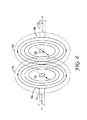
図6は、左側部70と右側部72とが示された導電性シールドからの磁界への作用を図示する側面透視図である。簡単に言うと、単一ループアンテナが導電性トレース74および76によって図6に図示されている。なお導電性シールドの影響に関して、双ループアンテナを、双ループに関連する半径間の平均と等しい半径を有する単一ループアンテナとして論理的に見なし得る。
FIG. 6 is a side perspective view illustrating the effect on the magnetic field from the conductive shield with the
図6に示すように、導電性トレース74および76内の電流Iは、それぞれの磁界82および84を生成する。特に磁界82、84は、それぞれ左側部70および右側部72の遮蔽作用がなければそれぞれ領域78、80に延びることもある。なお、このように左側部70および右側部72を導電性トレース74および76に近く配置するほど、合成磁界が形成される外側範囲をより限定することになる。さらに左側部70および右側部72を、導電性トレース74および76に近く配置するほど、磁界82、84が反対導電性トレースに向かって内側に延びる範囲をより限定することになる。この単一ループアンテナの場合の全体通信ゾーンは、磁界82および84のほぼ合計である。
As shown in FIG. 6, the current I in the conductive traces 74 and 76 generates the respective
この理由のため、D3(図5)を磁界82、84(図6)が重複するのに必要な最小距離を超えるように選択して、磁界強度がRFID通信に十分なループ内で達成されるようにする。
For this reason, D3 (FIG. 5) is selected to exceed the minimum distance required for the
一実施形態において、例えばD3を以下のようにD1とD2の平均とほぼ等しくなるように選択する。
D3≧(D1+D2)/2 (1)
さらに、D2をほぼ1.5*D1と等しくなるように選択する。例えば、D1、D2およびD3はそれぞれ2インチ(5.08cm)、3.5インチ(8.89cm)および2.75インチ(6.98cm)と等しい場合がある。距離D3に対するこの特定の選択により、内側ループ62および外側ループ64(図5)によって生成された合成磁界は、これらのループから内側および外側の両方向に延びてアンテナ60を十分な強度で全体的に覆い、RFID通信を達成することができる。
In one embodiment, for example, D3 is selected to be approximately equal to the average of D1 and D2, as follows:
D3 ≧ (D1 + D2) / 2 (1)
In addition, D2 is selected to be approximately equal to 1.5 * D1. For example, D1, D2, and D3 may be equal to 2 inches (5.08 cm), 3.5 inches (8.89 cm), and 2.75 inches (6.98 cm), respectively. With this particular choice for distance D3, the resultant magnetic field generated by
図7は導電性シールドの磁界整形作用を示す他の側面透視図である。具体的には図7はアンテナ94により生成されて、導電性シールドにより整形された合成電磁界90を図示し、導電性シールドの左側部92Aと右側部92Bが示されている。図示のように導電性シールドは、電磁界90がアンテナ94から外側に延びる範囲を限定することにより、規定された通信ゾーンの水平周縁部の下方に位置するRFIDタグの不用意な読み取りを防止する。
FIG. 7 is another side perspective view showing the magnetic field shaping action of the conductive shield. Specifically, FIG. 7 illustrates a synthetic
図8Aは、アンテナ102と導電性シールド104とが表面106の下方に載置された、返却/貸出領域100の一実施形態の側面図を示す透視図である。この例では、アンテナ102と導電性シールド104とが、表面106の上方にRFIDタグ通信ゾーン107を生成する。表面106は、通信ゾーンの周縁部を識別する視覚標識を含み得る。このようにして、導電性シールド104は規定された通信ゾーン107を超える領域108におけるRFIDタグの不用意な読み取りを防止する。
FIG. 8A is a perspective view illustrating a side view of one embodiment of the return /
図8Bは、返却/貸出領域110の他の実施形態の側面図を図示する透視図である。この例では、机面116は凹部120を形成し、その下方にアンテナ112が載置されている。導電性シールド114は、机面116の非凹部上にアンテナ112を取り囲むように載置されている。この例ではアンテナ112と導電性シールド114とがRFIDタグ通信ゾーン117を生成し、導電性シールドは規定された通信ゾーンを超える領域118におけるRFIDタグの不用意な読み取りを防止する。他の実施形態では、机面116は凹部120を形成せず、アンテナ112は机面の下方に載置される。
FIG. 8B is a perspective view illustrating a side view of another embodiment of the return /
本発明の様々な実施形態を説明した。これらおよび他の実施形態は以下の特許請求項の範囲内にある。 Various embodiments of the invention have been described. These and other embodiments are within the scope of the following claims.
Claims (16)
前記アンテナの周囲であって、前記アンテナに平行な面内に位置決めされた、実質的に連続する導電性シールドと、
を備えるRFIDシステム。 An antenna that forms an electromagnetic field for communication with a radio frequency identification (RFID) tag, the antenna having a substantially planar shape;
A substantially continuous conductive shield positioned in a plane around the antenna and parallel to the antenna;
RFID system comprising:
前記RFID問い合わせ装置から検索した前記情報を処理する計算装置と、
をさらに備える請求項1に記載のRFIDシステム。 An RFID interrogation device coupled to the antenna for interrogating the RFID tag to obtain information about the article;
A computing device for processing the information retrieved from the RFID inquiry device;
The RFID system according to claim 1, further comprising:
Applications Claiming Priority (2)
| Application Number | Priority Date | Filing Date | Title |
|---|---|---|---|
| US10/784,109 US7421245B2 (en) | 2004-02-20 | 2004-02-20 | Field-shaping shielding for radio frequency identification (RFID) system |
| PCT/US2005/000439 WO2005083836A1 (en) | 2004-02-20 | 2005-01-07 | Field-shaping shielding for radio frequency identification (rfid) system |
Publications (2)
| Publication Number | Publication Date |
|---|---|
| JP2007523563A true JP2007523563A (en) | 2007-08-16 |
| JP2007523563A5 JP2007523563A5 (en) | 2008-02-21 |
Family
ID=34861405
Family Applications (1)
| Application Number | Title | Priority Date | Filing Date |
|---|---|---|---|
| JP2006554090A Pending JP2007523563A (en) | 2004-02-20 | 2005-01-07 | Magnetic field shaping shielding for radio frequency identification (RFID) systems |
Country Status (15)
| Country | Link |
|---|---|
| US (1) | US7421245B2 (en) |
| EP (1) | EP1723697B1 (en) |
| JP (1) | JP2007523563A (en) |
| KR (1) | KR20070011314A (en) |
| CN (1) | CN1954462A (en) |
| AR (1) | AR047687A1 (en) |
| AT (1) | ATE417381T1 (en) |
| AU (1) | AU2005217933A1 (en) |
| BR (1) | BRPI0507833A (en) |
| CA (1) | CA2556932A1 (en) |
| DE (1) | DE602005011583D1 (en) |
| ES (1) | ES2317187T3 (en) |
| NZ (1) | NZ549370A (en) |
| TW (1) | TW200529737A (en) |
| WO (1) | WO2005083836A1 (en) |
Cited By (3)
| Publication number | Priority date | Publication date | Assignee | Title |
|---|---|---|---|---|
| WO2009101750A1 (en) * | 2008-02-12 | 2009-08-20 | Nec Corporation | Loop antenna and immunity test method |
| JP2011146836A (en) * | 2010-01-13 | 2011-07-28 | Alps Electric Co Ltd | Input device with antenna and electronic device having the same |
| US10931006B2 (en) | 2018-06-07 | 2021-02-23 | Kabushiki Kaisha Toshiba | Chip antenna |
Families Citing this family (33)
| Publication number | Priority date | Publication date | Assignee | Title |
|---|---|---|---|---|
| US7342496B2 (en) | 2000-01-24 | 2008-03-11 | Nextreme Llc | RF-enabled pallet |
| US8077040B2 (en) | 2000-01-24 | 2011-12-13 | Nextreme, Llc | RF-enabled pallet |
| JP3982476B2 (en) * | 2003-10-01 | 2007-09-26 | ソニー株式会社 | Communications system |
| JP4742546B2 (en) * | 2004-09-13 | 2011-08-10 | オムロン株式会社 | Goods conveying material |
| WO2006075398A1 (en) * | 2005-01-17 | 2006-07-20 | Fujitsu Limited | Communication device and communication method |
| WO2007149998A2 (en) * | 2006-06-21 | 2007-12-27 | Neology, Inc. | Systems and methods for interrogator multiple radio frequency identification enabled documents |
| FR2904880B1 (en) * | 2006-08-11 | 2008-10-10 | Ask Sa | SECURITY DEVICE INTEGRATED WITH CONTACTLESS OBJECT OF SECURE DOCUMENT TYPE WITH RADIO FREQUENCY DEVICE. |
| GB0802729D0 (en) * | 2008-02-14 | 2008-03-26 | Isis Innovation | Resonant reflector assembly and method |
| US8076593B2 (en) | 2008-03-28 | 2011-12-13 | David Centner | Apparatus and method for supporting and shielding a wireless device |
| US9515494B2 (en) | 2008-09-27 | 2016-12-06 | Witricity Corporation | Wireless power system including impedance matching network |
| US9160203B2 (en) | 2008-09-27 | 2015-10-13 | Witricity Corporation | Wireless powered television |
| US20100232132A1 (en) * | 2009-03-16 | 2010-09-16 | Highway Toll Administration, Llc | Flexible Transponder Holder |
| US8514059B2 (en) * | 2009-08-06 | 2013-08-20 | Highway Toll Administration, Llc | Transponder holder for controlling the operation of a transponder |
| US8353759B2 (en) | 2009-10-16 | 2013-01-15 | Igt | Shape control of magentic fields for table games |
| EP2529364B1 (en) | 2010-01-29 | 2014-07-02 | Avery Dennison Corporation | Rfid/nfc panel and/or array used in smart signage applications and method of using |
| US10977965B2 (en) | 2010-01-29 | 2021-04-13 | Avery Dennison Retail Information Services, Llc | Smart sign box using electronic interactions |
| WO2013033522A1 (en) | 2011-09-01 | 2013-03-07 | Avery Dennison Corporation | Apparatus, system and method for consumer tracking |
| US8659494B2 (en) | 2011-11-07 | 2014-02-25 | Symbol Technologies, Inc. | Rotating-polarization reflector-backed RFID loop antenna apparatus and method |
| WO2014039089A1 (en) * | 2012-09-10 | 2014-03-13 | Avery Dennison Corporation | Method for preventing unauthorized diversion of nfc tags |
| EP3214572B1 (en) | 2012-10-18 | 2020-01-29 | Avery Dennison Corporation | System and apparatus for nfc security |
| US9767329B2 (en) | 2012-11-19 | 2017-09-19 | Avery Dennison Retail Information Services, Llc | NFC tags with proximity detection |
| WO2014088323A1 (en) * | 2012-12-04 | 2014-06-12 | Samsung Electronics Co., Ltd. | Antenna for wireless power transmission and near field communication |
| US9165235B2 (en) | 2013-05-21 | 2015-10-20 | Garble, LLC | Method and apparatus for protecting information in magnetic strip and RFID cards from fraudulent scanning |
| US20150162957A1 (en) * | 2013-12-05 | 2015-06-11 | WaveMark, Inc. | Scanning station utilizing passive near-field communication RF coupling system for scanning RFID tags |
| FR3023983B1 (en) | 2014-07-16 | 2017-12-08 | Oberthur Technologies | RFID TRANSPONDER ELECTRONIC ENTITY |
| KR20160063191A (en) * | 2014-11-26 | 2016-06-03 | 삼성전기주식회사 | Antenna device and Near field communication device including the same |
| FR3030908B1 (en) * | 2014-12-18 | 2016-12-09 | Stmicroelectronics Rousset | ANTENNA FOR ELECTRONIC DEVICE |
| CN207459190U (en) * | 2015-01-15 | 2018-06-05 | 株式会社村田制作所 | Antenna assembly |
| KR102405446B1 (en) * | 2015-08-10 | 2022-06-08 | 삼성전자주식회사 | Antenna device and electronic device |
| KR101754742B1 (en) * | 2016-02-29 | 2017-07-06 | 주식회사 알앤엠테크 | Casino chips reading apparatus in casino tables |
| DE102018112570A1 (en) * | 2018-05-25 | 2019-11-28 | Ebm-Papst Mulfingen Gmbh & Co. Kg | Device and method for sending and receiving data of a passive RFID tag |
| US11769938B2 (en) * | 2018-06-27 | 2023-09-26 | Avery Dennison Retail Information Services Llc | RFID tags operating in the high frequency band |
| US20200364420A1 (en) * | 2019-05-17 | 2020-11-19 | Storeroom Logix, LLC | Autonomous rfid storage system |
Family Cites Families (21)
| Publication number | Priority date | Publication date | Assignee | Title |
|---|---|---|---|---|
| US4260990A (en) * | 1979-11-08 | 1981-04-07 | Lichtblau G J | Asymmetrical antennas for use in electronic security systems |
| US4373163A (en) * | 1980-07-14 | 1983-02-08 | I.D. Engineering, Inc. | Loop antenna for security systems |
| JP2528517Y2 (en) * | 1990-11-21 | 1997-03-12 | 日本板硝子株式会社 | Window glass antenna |
| US5142292A (en) * | 1991-08-05 | 1992-08-25 | Checkpoint Systems, Inc. | Coplanar multiple loop antenna for electronic article surveillance systems |
| US5404147A (en) | 1992-10-28 | 1995-04-04 | Sensormatic Electronics Corporation | EAS system loop antenna having three loops of different area |
| ATE190431T1 (en) * | 1994-04-18 | 2000-03-15 | Alfa Laval Agri Ab | ANTENNA ARRANGEMENT |
| AU3741497A (en) | 1996-07-29 | 1998-02-20 | Motorola, Inc. | Magnetic field antenna and method for field cancellation |
| US5914692A (en) | 1997-01-14 | 1999-06-22 | Checkpoint Systems, Inc. | Multiple loop antenna with crossover element having a pair of spaced, parallel conductors for electrically connecting the multiple loops |
| US5940043A (en) * | 1997-02-21 | 1999-08-17 | Sensormatic Electronics Corporation | Unidirectional field antenna for identification system |
| CH691098A5 (en) * | 1997-03-24 | 2001-04-12 | Em Microelectronic Marin Sa | monolithic structure of integrated circuit and antenna coil provided with a peripheral protective ring. |
| US6285327B1 (en) * | 1998-04-21 | 2001-09-04 | Qualcomm Incorporated | Parasitic element for a substrate antenna |
| US5977875A (en) * | 1998-08-31 | 1999-11-02 | Magnex Corporation | Collective objects management system using R.F. object indentification |
| US6147655A (en) * | 1998-11-05 | 2000-11-14 | Single Chip Systems Corporation | Flat loop antenna in a single plane for use in radio frequency identification tags |
| US6714121B1 (en) * | 1999-08-09 | 2004-03-30 | Micron Technology, Inc. | RFID material tracking method and apparatus |
| WO2001026180A1 (en) | 1999-10-04 | 2001-04-12 | Amerasia International Technology, Inc. | Tamper-resistant wireless article including an antenna |
| US6307517B1 (en) * | 2000-06-13 | 2001-10-23 | Applied Wireless Identifications Group, Inc. | Metal compensated radio frequency identification reader |
| FR2824018B1 (en) * | 2001-04-26 | 2003-07-04 | Arjo Wiggins Sa | COVER INCORPORATING A RADIOFREQUENCY IDENTIFICATION DEVICE |
| US20020180588A1 (en) * | 2001-06-05 | 2002-12-05 | Erickson David P. | Radio frequency identification in document management |
| US6567050B1 (en) * | 2001-12-17 | 2003-05-20 | Briggs James B | Loop antenna compensator |
| US7187288B2 (en) * | 2002-03-18 | 2007-03-06 | Paratek Microwave, Inc. | RFID tag reading system and method |
| US6700547B2 (en) * | 2002-04-12 | 2004-03-02 | Digital Angel Corporation | Multidirectional walkthrough antenna |
-
2004
- 2004-02-20 US US10/784,109 patent/US7421245B2/en not_active Expired - Fee Related
-
2005
- 2005-01-07 EP EP05705207A patent/EP1723697B1/en not_active Not-in-force
- 2005-01-07 DE DE602005011583T patent/DE602005011583D1/en active Active
- 2005-01-07 NZ NZ549370A patent/NZ549370A/en unknown
- 2005-01-07 AT AT05705207T patent/ATE417381T1/en not_active IP Right Cessation
- 2005-01-07 BR BRPI0507833-4A patent/BRPI0507833A/en not_active IP Right Cessation
- 2005-01-07 CN CNA2005800090098A patent/CN1954462A/en active Pending
- 2005-01-07 AU AU2005217933A patent/AU2005217933A1/en not_active Abandoned
- 2005-01-07 KR KR1020067019228A patent/KR20070011314A/en not_active Application Discontinuation
- 2005-01-07 JP JP2006554090A patent/JP2007523563A/en active Pending
- 2005-01-07 WO PCT/US2005/000439 patent/WO2005083836A1/en active Search and Examination
- 2005-01-07 ES ES05705207T patent/ES2317187T3/en active Active
- 2005-01-07 CA CA002556932A patent/CA2556932A1/en not_active Abandoned
- 2005-01-25 TW TW094102216A patent/TW200529737A/en unknown
- 2005-02-18 AR ARP050100590A patent/AR047687A1/en unknown
Cited By (4)
| Publication number | Priority date | Publication date | Assignee | Title |
|---|---|---|---|---|
| WO2009101750A1 (en) * | 2008-02-12 | 2009-08-20 | Nec Corporation | Loop antenna and immunity test method |
| JP5504894B2 (en) * | 2008-02-12 | 2014-05-28 | 日本電気株式会社 | Loop antenna and immunity test method |
| JP2011146836A (en) * | 2010-01-13 | 2011-07-28 | Alps Electric Co Ltd | Input device with antenna and electronic device having the same |
| US10931006B2 (en) | 2018-06-07 | 2021-02-23 | Kabushiki Kaisha Toshiba | Chip antenna |
Also Published As
| Publication number | Publication date |
|---|---|
| KR20070011314A (en) | 2007-01-24 |
| US7421245B2 (en) | 2008-09-02 |
| AR047687A1 (en) | 2006-02-01 |
| CN1954462A (en) | 2007-04-25 |
| EP1723697A1 (en) | 2006-11-22 |
| DE602005011583D1 (en) | 2009-01-22 |
| ATE417381T1 (en) | 2008-12-15 |
| EP1723697B1 (en) | 2008-12-10 |
| TW200529737A (en) | 2005-09-01 |
| AU2005217933A1 (en) | 2005-09-09 |
| BRPI0507833A (en) | 2007-07-10 |
| WO2005083836A1 (en) | 2005-09-09 |
| US20050186902A1 (en) | 2005-08-25 |
| ES2317187T3 (en) | 2009-04-16 |
| NZ549370A (en) | 2008-03-28 |
| CA2556932A1 (en) | 2005-09-09 |
Similar Documents
| Publication | Publication Date | Title |
|---|---|---|
| JP2007523563A (en) | Magnetic field shaping shielding for radio frequency identification (RFID) systems | |
| JP2007523562A (en) | Multiple loop antenna for radio frequency identification (RFID) communication | |
| US6861993B2 (en) | Multi-loop antenna for radio-frequency identification | |
| US20090085750A1 (en) | Extended RFID tag | |
| US20050212707A1 (en) | Radio frequency identification tags with compensating elements | |
| EP1298573A2 (en) | Radio frequency identification system comprising a plurality of antennas | |
| KR20070058679A (en) | A passport reader for processing a passport having an rfid element | |
| US8451126B2 (en) | Combination electronic article surveillance/radio frequency identification antenna and method | |
| MXPA06009458A (en) | Field-shaping shielding for radio frequency identification (rfid) system | |
| MXPA06009459A (en) | Multi-loop antenna for radio frequency identification (rfid) communication | |
| AU2013200855A1 (en) | Multi-loop antenna for radio-frequency identification |
Legal Events
| Date | Code | Title | Description |
|---|---|---|---|
| A521 | Request for written amendment filed |
Free format text: JAPANESE INTERMEDIATE CODE: A523 Effective date: 20071227 |
|
| A621 | Written request for application examination |
Free format text: JAPANESE INTERMEDIATE CODE: A621 Effective date: 20071227 |
|
| A131 | Notification of reasons for refusal |
Free format text: JAPANESE INTERMEDIATE CODE: A131 Effective date: 20081014 |
|
| A02 | Decision of refusal |
Free format text: JAPANESE INTERMEDIATE CODE: A02 Effective date: 20090310 |